Embed Size (px)
Citation preview

Research Paper
Electrical imaging of the quantum Hall state
A. Yacoby†, H.F. Hess‡, T.A. Fulton* , L.N. Pfeiffer, K.W. West
Bell Laboratories, Lucent Technologies, 600 Mountain Ave, Murray Hill, NJ 07974, USA
Received 1 March 1999; accepted 16 March 1999 by A. Pinkzuk
Abstract
Microscopic images of the local electron compressibility, electrostatic potential, and current-induced Hall voltage of a two-dimensional sheet of electrons in the quantum Hall regime are acquired using a single-electron transistor as a scanned probe.Regions identified as differing in quantum state (Landau level) occupancy of the electrons appear in interrelated ways in all ofthese properties. The compressibility images show quasi-insulating “incompressible” strips, associated with edge states thatbound these regions. These strips follow the contours of a constant electron density that match exact occupancy of Landaulevels, and shift accordingly with magnetic field and electron density changes. The potential distribution has an overallcorrelation with the density contours marked by the incompressible strips and a step across the strips that provides a directmeasure of the energy gap between Landau levels. The Hall voltage and the inferred current flow patterns are also guided bythese strips.q 1999 Elsevier Science Ltd. All rights reserved.
Keywords:A. Heterojunctions; B. Scanning tunneling microscopy; C. Quantum Hall effect
1. Introduction
The physical properties of any macroscopicobject are quantum-mechanical in origin. Whilethis cause-and-effect relation is usually hard tosee, in a few exceptional cases it is quite clear,as in the integer quantum Hall effect. Here anordinary measurement of the currentI and voltageV in a macroscopic, even though effectively two-dimensional, semiconductor device gives a ratio ofI to V that is an exact multiple of the ratio offundamental constantse2/h, where e is the
electronic charge and h Planck’s constant. Thesame result is found over a wide range of deviceand experimental conditions. This quantummechanical behavior writ large has been intenselystudied since its discovery in 1980 [1]. In typicalexperiments, the device is a GaAs–AlGaAsheterojunction having a sheet of high-mobilityelectrons confined in a potential well just belowthe surface. At low temperatures, the electrons arerestricted, in a quantum mechanical sense, to atwo-dimensional motion parallel to the surface.This two-dimensional electron gas (2DEG) issubjected to a magnetic fieldB . t 1 T at alow temperature, , 10 K. Four contacts on theperimeter of the 2DEG are usedalternately as Iand V terminals, and the “Hall” conductanceI/V ismeasured asB is scanned. WheneverB approxi-mately satisfiesB/(h/e) � n/N, where n is theelectron density andN � 1,2,3,…, the Hall
Solid State Communications 111 (1999) 1–13
0038-1098/99/$ - see front matterq 1999 Elsevier Science Ltd. All rights reserved.PII: S0038-1098(99)00139-8
PERGAMON
* Corresponding author. Tel.:1 1-908-582-3463; fax:1 1-908-582-7660.
E-mail address:[email protected] (T.A. Fulton)† Present address: The Weizmann Institute of Science, Rehovot,
Israel‡ Present address: Phasemetrics Incorporated, 10260 Sorrento
Valley Rd., San Diego, CA 92121, USA.

conductance takes on the exact valueNe2/h over aconsiderable range ofB around this value†,‡.
A succinct theoretical explanation of this behaviorwas provided shortly after the first experiments, basedon a symmetry argument [2]. Since then, a moredetailed picture of what happens has emerged [3].To a first approximation, the 2DEG is a gas of non-interacting electrons confined to a plane. Owing to thelarge magnetic fieldB, these electrons occupy statesof quantized cyclotron motion called Landau levels.These levels are separated in energy by gaps propor-tional toB. Each level can accommodate up toB/(h/e)electrons/unit area. The population of the levels isdescribed by thefilling factor n � n/B/(h/e). Thus,the condition of quantized conductance correspondsto an integer filling factor, meaning that the lowestNLandau levels are completely full, at low tempera-tures, and the rest empty§. This correspondence doesnot, however, explain the surprising persistence of thequantized conductance over a range ofB and insamples of varying density, which is the essence ofthe quantum Hall effect. To account for this, a furtherconcept ofedge states[4] is required, which refers tothose one-dimensional quantum-mechanical statesthat lie along contours of density that correspond tointeger filling factors. These states have a form corre-sponding to the classical cycloidal motion of electronsin anE × B field, associated with current flow. Indeedone main result of the present work is to provide sub-micron images of the “incompressible strips” that liealong the individual edge states, subdividing the2DEG into regions of differing Landau-level occu-pancy, and further to show how these strips act toguide patterns of Hall voltage and current.
The concept of edge states involves the non-uniform nature of the electron density,n. In realdevices,n is depleted to zero near sample edges or
biased top gates by the increase in a confiningpotential. Additional, less-extreme non-uniformityin n arises elsewhere from disorder in the poten-tial, and from causes occurring in sample fabrica-tion and treatment. Consequently, exactly integerfilling factors n do not occur everywhere at once,but only in separate, narrow regions along thecontour lines of density, the edge-state contours,given by n � NB/(h/e), where N � 1,2,3,… (Fig.1). In the regions between the contours, the Fermilevel lies within a single Landau level.
The edge state associated withn �N will exist overa wide range ofB. At low B, its contour runs in thelow-n region, close to the edge. AsB increases, thecontour climbs inn, and eventually pulls away fromthe edge, following the topography ofn into the inter-ior (Fig. 1). At lowerB, there are several states alongthe edge at once, running between the electricalcontacts. This connection is lost when they moveinto the interior.
In a widely accepted picture, current injected at acontact tends to flow in the regions between theseedge-state contours, so-called edge channels. If thecontours run close to the edge, all the edge channelsin proximity to one contact will provide a continuouspath to a neighboring contact. It is thought that in thissituation the conductance between these two contactswill show quantized behavior. If, however, the outer-most contour wanders away into the interior betweenthese contacts, the connection provided by the asso-ciated edge channel is lost and so is the quantizedbehaviork [5].
For the older model of non-interacting electrons, anabrupt change in densityn occurs at the position of anedge state, where the Fermi level crosses a Landaulevel. However, when the electrostatic energy isconsidered, the density is found to have a smoother,near-classical form (Fig. 1), except at the edge-statecontours. These are marked by a narrowincompres-sible strip running along the contour [6–11]. Withinthis strip, the charge adjusts so that the density is fixedat n� NB/(h/e) (Fig. 1), and the 2DEG is incompres-sible, i.e. unable to screen changes in potential, some-what like an insulator. The relationship of the density
A. Yacoby et al. / Solid State Communications 111 (1999) 1–132
† Conductance steps are also observed, at lower temperatures, forfractional values ofN, particularly forN , 1. These involve themore exotic fractional quantum Hall effect.
‡ The related longitudinal resistance measured with adjacent pairsof contacts necessarily givesV/I � 0 over the same range. Otherproperties such as the specific heat and the magnetic moment alsoshow oscillatory, but not quantized, behavior with this same patternin B.
§ In this case, the Fermi energy is between Landau levels, where,due to a disorder, a small percentage of the states are not Landau-like but are localized in position and not involved in conduction.
k This is the net current. There are larger, oppositely flowingdiamagnetic currents on the two sides, which cancel except whenthe Fermi levels on the two sides are unequal.
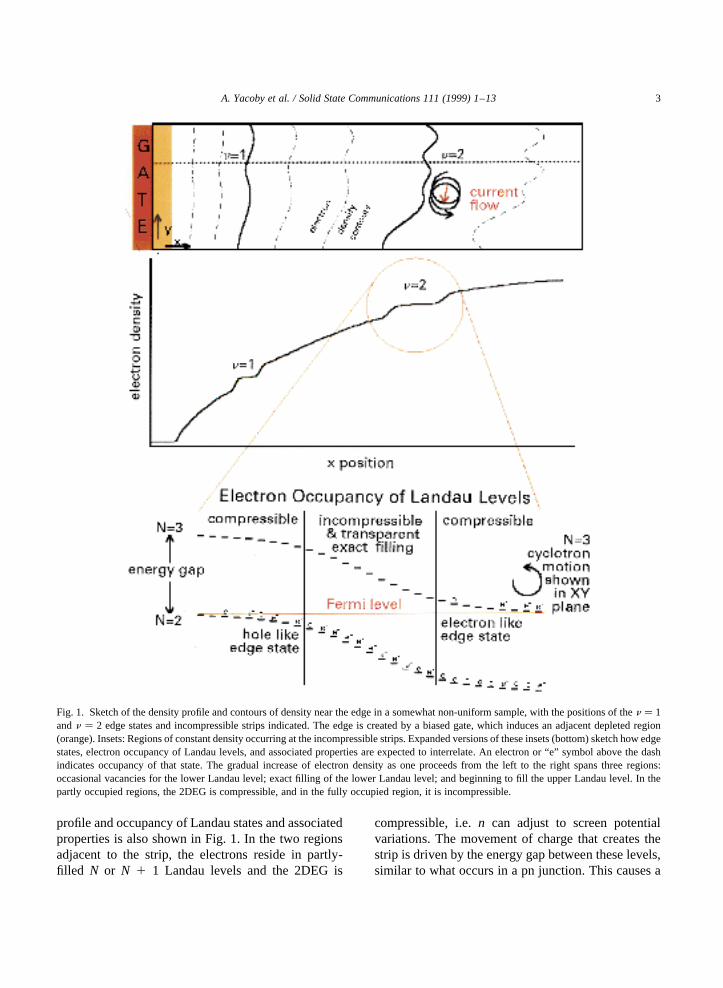
profile and occupancy of Landau states and associatedproperties is also shown in Fig. 1. In the two regionsadjacent to the strip, the electrons reside in partly-filled N or N 1 1 Landau levels and the 2DEG is
compressible, i.e.n can adjust to screen potentialvariations. The movement of charge that creates thestrip is driven by the energy gap between these levels,similar to what occurs in a pn junction. This causes a
A. Yacoby et al. / Solid State Communications 111 (1999) 1–13 3
Fig. 1. Sketch of the density profile and contours of density near the edge in a somewhat non-uniform sample, with the positions of then � 1andn � 2 edge states and incompressible strips indicated. The edge is created by a biased gate, which induces an adjacent depleted region(orange). Insets: Regions of constant density occurring at the incompressible strips. Expanded versions of these insets (bottom) sketch how edgestates, electron occupancy of Landau levels, and associated properties are expected to interrelate. An electron or “e” symbol above the dashindicates occupancy of that state. The gradual increase of electron density as one proceeds from the left to the right spans three regions:occasional vacancies for the lower Landau level; exact filling of the lower Landau level; and beginning to fill the upper Landau level. In thepartly occupied regions, the 2DEG is compressible, and in the fully occupied region, it is incompressible.

step in work function equal to this gap to appearacross the strip.
With direct imaging of the spatial structure of thequantum Hall effect, one can confirm critical assump-tions of current theoretical models and clarify howmicroscopic details influence the more standardmacroscopic conductivity measurements. The older,related question of whether the Hall voltage and trans-port current are confined to the edge of the sample ordistributed uniformly in the quantized regime simi-larly lends itself to imaging. Many interesting resultshave already been obtained in these directions,variously using multiple contacts [12], local heating[13], Pockels effect [14], breakdown [15], differentiallateral photoeffect [16–18], and inductive probing[19]. Most recently elegant work-function measure-ments have been made with a fixed single-electrontransistor (SET) [20]. Also, intriguing detailedscanned images oft 100 kHz charge accumulation
phenomena involving the electron compressibilityand resistivity in the quantum Hall regime havebeen obtained [21]. Finally, Hall voltages have beenimaged with good sensitivity on a fine scale usinga scanning electric-force probe [22] operated att 100 kHz.
In what follows a SET scanning electrometer [23] isused to map out, concurrently, three related propertiesof a 2DEG in the quantum Hall regime. These are theelectrostatic surface potentialVsurf, which is directlyrelated to the work function and hence to dopant ioni-zation and to the electron density, the “transparency”of the 2DEG to the electric field from a back gate,which probes the electron gas compressibility, and thevoltage, primarily a Hall voltage, induced by transportcurrent. The incompressible strips associated withedge states show up in related ways in all theseimages, especially the transparency, where theyallow us to map out the 2DEG electron density. An
A. Yacoby et al. / Solid State Communications 111 (1999) 1–134
Fig. 2. (A) Sketch of the SET probe suspended over the GaAs/AlGaAs heterostructure. The 2DEG is formed below the silicon dopants andabove a deeper (byt 5mm) back gate. (B) Schematic of the circuit of the SET bias, feedback and modulation electronics. A simple voltage-source plus-resistor circuit biases the SET to a voltaget VSET and a currentt ISET. The variations ofISET as sensed by the resistor are amplifiedand form the signal output. Three different lock-in amplifiers can record the transparency, Hall effect and calibration signals, simultaneously. Aswitch also allows direct measurement of the electrostatic potential by feedback of the signal to hold the SET current constant. TheVfSET
voltage is used to offset the tip vs. sample voltages such that potentials induced by work-function differences are minimized.

A. Yacoby et al. / Solid State Communications 111 (1999) 1–13 5
Fig
.3.
(A)M
icro
grap
h(7
0×11
0m
m)o
fthe
patte
rned
sam
ple
show
ing
seve
nto
pga
tes
over
lapp
ing
the
2DE
G,w
hich
occu
pies
the
uppe
rand
cent
er-r
ight
regi
on.O
hmic
cont
acts
toth
e2D
EG
are
inte
rspe
rsed
betw
een
the
gate
s.(B
)an
d(C
)sh
ow5
×15
mm
and
5×5m
mtr
ansp
aren
cyim
ages
ofde
plet
ed2D
EG
regi
ons
(inar
bitr
ary
units
)fo
rto
p-ga
tebi
ases
of2
0.4
and2
0.1
V,
resp
ectiv
ely.

A. Yacoby et al. / Solid State Communications 111 (1999) 1–136
Fig
.4.
(A)T
ypic
alel
ectr
osta
ticpo
tent
ial,
orVsu
rfim
age,
ona
1.0
Vsc
ale,
ofth
esa
mpl
esh
owin
gth
ele
ftan
drig
htga
tes,
for
B�
4.48
T.S
uch
imag
esar
eob
tain
edco
ncur
rent
lyw
ithea
chtr
ansp
aren
cyim
age,
butd
ono
tcha
nge
notic
eabl
yon
this
scal
e.(B
–F
,H,I
and
J).T
rans
pare
ncy
imag
esfo
rdiff
eren
tmag
netic
field
sar
ound
fillin
gfa
ctor
sofn�
2,1
and
4.T
hetr
ansp
aren
cy,s
how
nin
arbi
trar
yun
its,i
sa
mea
sure
ofsc
reen
ing
ofth
em
odul
ated
back
-gat
evo
ltage
see
page
10,f
ootn
ote
‡ .(G
)T
heel
ectr
ost
atic
pote
ntia
lof(
A)
show
nw
itht×
10hi
gher
sens
itivi
tyw
ithtw
oco
ntou
rlin
es.T
hebl
ack
mas
ksin
the
figur
ean
dF
ig.5
outli
neth
epo
sitio
nof
the
gate
s.T
hew
eak
sign
als
seen
atth
ega
tee
dges
inth
etr
ansp
aren
cyim
ages
are
due
tolim
itatio
nsof
the
scan
ning
SE
Tel
ectr
oni
csin
stee
pvo
ltage
grad
ient
s.S
ome
imag
esal
sosh
owth
eef
fect
ofa
smal
lac
volta
geco
mpo
nent
atth
eba
ck-g
ate
freq
uenc
yon
the
left
gate
.

A. Yacoby et al. / Solid State Communications 111 (1999) 1–13 7
Fig
.5.
(A)–
(E)A
tran
spar
ency
sequ
ence
atB�
5.2
Tin
whi
chth
eba
ckga
teis
empl
oyed
tode
crea
seth
ede
nsity
byt
1.3
×1010
elec
tro
ns/c
m2 .The
inco
mpr
essi
ble
strip
she
rear
efo
r n�
1.(F
)Ask
etch
show
ing
how
elec
tro
nsfil
lthe
avai
labl
eLa
ndau
leve
lsta
tes
asin
Fig
.1.I
tis
agu
ide
toth
eda
taof
(G).
(G)D
ata
show
ing
the
pote
ntia
lste
pan
dco
rres
pond
ing
tran
spar
ency
sign
atur
ecr
eate
dby
pass
ing
ast
ripun
dert
heS
ET
(hel
dat
afix
edpo
int)
byde
crea
sing
dens
ityw
ithth
eba
ckga
te.(
H)C
olor
-sca
lepl
otsh
owin
gth
etr
ansp
aren
cysi
gnal
vs.t
heba
ck-g
ate-
indu
ced
dens
itych
ange
and
the
mag
netic
field
ata
fixed
poin
t.T
his
show
sth
elo
cus
ofm
agne
ticfie
ldvs
.ele
ctro
nde
nsity
forw
hich
the
tran
spar
ency
strip
does
not
shift
.T
heex
pect
edsl
ope,
indi
cate
dby
the
dotte
dlin
e,is
h/N
ew
ithN�
2fo
rth
ese
cond
Land
aule
vel.

A. Yacoby et al. / Solid State Communications 111 (1999) 1–138
Fig
.6.
(A)–
(D)I
mag
eof
the
volta
gein
duce
din
the
sam
ple
byan
appl
ied
curr
entu
nder
ara
nge
ofm
agne
ticfie
lds
near
n�
2.T
heH
allv
olta
geap
pear
sro
ughl
ylin
ear
atth
ehi
ghes
tfie
ld(A
),bu
tbe
com
esin
crea
sing
lyno
n-lin
ear
asth
efie
ldde
crea
ses
(B)–
(D).
Cor
resp
ondi
ngtr
ansp
aren
cyim
ages
(F)
and
(G)
show
how
the
curr
ent
flow
int
erac
tsw
ithth
ein
com
pres
sibl
est
ripan
dfo
rms
the
patte
rns
sket
ched
in(H
).T
hese
curr
entfl
owve
ctor
sar
ein
ferr
edfr
omth
esp
atia
lgra
dien
tin
the
Hal
lpot
entia
l.T
hese
data
wer
eta
ken
ina
sepa
rate
cool
-dow
nfr
omth
ose
ofF
igs.
4an
d5.

extensive study of the field and density dependence,and the interrelation of all three imaged quantitiesgives a cohesive physical picture of the quantumHall effect, whereby the distribution of dopant ioniza-tion, electron density, Landau level occupancy andcurrent flow can be understood in unison.
2. The experimental system
In our GaAs/AlGaAs heterojunction sample, a2DEG forms on the GaAs side of the interface,100 nm below the surface (Fig. 2(A))†. Silicondopants in the upper part of the AlGaAs supply elec-trons both to states at the surface and to the 2DEG‡,§.Several metal gates (TiAu) are patterned on thesurface (Fig. 3(A)). These enable us to deplete the2DEG and to restrict current flow to specific regions.Additionally, a back gate is formed by a 1mm thickn1 layer, 5.4mm below the 2DEG, allowing us todecrease and/or modulate the electron density. Thedata of Figs. 4–6 are obtained from our main sample,whose mobility was 4× 106 cm2/V s, before pattern-ing, and in which the range of density, measuredlocally with the SET probe, is 0.8–1.25× 10¹¹ elec-trons/cm2. This sample showed the usual quantizedconductances, which occurred at fields correspondingto somewhat larger densities. The data of Fig. 3 camefrom a second sample of the same physical configura-tion, but of a lower density, estimated ast 4 ×10¹⁰ electrons/cm2.
The combination of good electrostatic sensitivity atd.c. and low frequency (, 100mV/Hz1/2) at ,100 Hz, which minimizes resistive effects, andsub-micron resolution necessary for the present
experiments is obtained by using a SETk [24,25] asa scanning electric field probe (Fig. 2(A)). It is fabri-cated on the flat,t 100 nm diameter tip of a taperedglass fiber, which hoverst 100–200 nm above thesample surface¶. Any changing potential under theprobe modulates the current through the SET. Bymonitoring this current while scanning the probe ina raster pattern across the surface, one can construct“electric-field” images ofVsurf, which is a measure ofthe electric-field flux emanating from the surface [23].For the most part this is accomplished with a samplevoltage feedback (Vb � 2 Vsurf) that nulls any SETresponse (Fig. 2(B)). To extract the mV-level trans-parency and transport signals from the large staticsignals of biased surface gates (t 1 V) and fluctuatingsurface and dopant charges (t 50 meV) [23], we uselow-frequency modulation and lock-in detectionschemes (Fig. 2(B)). For the transport signals, ana.c. currentd I is passed through the 2DEG and theinduced voltage,dVsurf, is measured, givingdVsurf/d I.Similarly an a.c. back-gate voltagedVBG that leaksthrough the 2DEG and is not fully screened givesthe transparency signal,dVsurf/dVBG. This transpar-ency signal is related to the compressibilityk of the2DEG bydVsurf/dVBG� C/ek , whereC is the capaci-tance between the 2DEG and the back gate [26,27].Apparent transparency signals can also arise if theresistance of the current paths in the 2DEG is solarge that the charging of an area is not able to followthe a.c. gate voltage. As described later, we sometimessee out-of-phase or unusually-large signals that weascribe to this cause, but most of the transparencyfeatures appear not to involve resistive effects.
3. Low-field transparency
An example of transparency measurements atzero applied magnetic field is given in Fig. 3. Themicrograph of Fig. 3(A) shows a set of top gates over-lapping the nominally uniform 2DEG. The SET israster-scanned across the area indicated by the redline. Any signal penetrating the 2DEG from an a.c.back-gate voltage is recorded. Two representativecolor-scale images of these signals appear in Fig.3(B) and (C). These correspond to different top-gatebiases. Regions of large signal (white) occur wherethe back gate is unscreened because the 2DEG is fully
A. Yacoby et al. / Solid State Communications 111 (1999) 1–13 9
† Since the 2DEG is buried byt 100 nm, the apparent width of2DEG features exceeds that of surface features byt 200 nm.
‡ The density of 2DEG negative charge is equal to the net positivecharge density in the donor layer and the surface.
§ Measurements are made in the dark to avoid the formation of aparallel conduction in the donor layer.k The signal levels here correspond tot 0.01e/0.001e induced on
the SET island at dc/low frequency a.c.¶ Tip size and heights are estimated from the capacitance and the
observed spatial resolution. In most images, surface features such asgate edges aret 600 nm wide. All conductors on the sample aregiven a common bias offset relative to the tip oft 2 0.8 V toroughly cancel the work-function difference between the 2DEG andthe tip, so as to minimize the charge induced by the tip. Measure-ments are made at a temperature oft 0.8 K.
depleted by the fringing fields of the top gates. Theareas of no signal (dark red) occur where the back gateis screened, either in conducting areas where the2DEG is not fully depleted or over the T-shapedmetal gates. Areas of intermediate color and signallevel next to the gates are unresolved, narrow depletedregions caused by the gate bias [9]. These signalsincrease in strength and coverage as the gate bias ismade more negative, and eventually cover the entirearea between the gates. The non-uniform depletion inthis region shows, qualitatively, that the density hereis also non-uniform. Note that when areas near theconstriction are fully depleted, an open circuitwould result in a contact-based measurement.
4. Transparency and surface potential in thequantum Hall regime
Clear-cut microscopic structure arising from theincompressible strips appears in the images of thetransparency presented in Figs. 4 and 5. These areobtained from our main sample in the region shownby the blue line in Fig. 3(A), and cover a range ofmagnetic fields corresponding to filling factors from1 to 4. For orientation, a typical image of theVsurf inthis region is shown in Fig. 4(A), and on an expandedscale in Fig. 4(G). Here the gates show up against the2DEG background owing to their different work func-tions and their biases, 0 and2 0.6 V for the left- andright-hand gates. The electron density under and justadjacent to the latter gate is depleted to zero by thebias, forming an edge to the 2DEG.
The transparency images of this region (remainingpanels of Fig. 4) reveal compressible and incompres-sible phases of the 2DEG. The upper row (Fig. 4)corresponds to magnetic fields nearn � 2†. Theseshow regions of strong signal (lighter colors) wherethe a.c. bias of the back gate penetrates the 2DEG. Theregions appear as isolated, non-uniform strips thatmeander across the image. In the rest of the region,there is no signal (dark red) as the 2DEG screens theback gate. By definition, the regions of signal are
incompressible areas of 2DEG surrounded bycompressible areas. The strips shift with increasingmagnetic field, and, allowing for some drift andhysteresis, form a pattern resembling contour lines.Based on this, and the overall behavior describedbelow, we identify these as the incompressible stripsthat lie along then � 2 edge states, marking thecontours of electron density that correspond to thefilling n � n/B/(h/e) � 2. Similar strips of the samegeneral shape are observed at double and half themagnetic field, and correspond to then � 1 andn �4 states (Fig. 4(H)–(J))‡,§.
One expects these strips to lie not just in the openareas, but as much or more so near the edge of the2DEG, along the right-hand gate (shown masked). Ifthese strips are too close to the gate, however, then thesignals are screened by the gate metal and cannot beseen with our present sensitivity. Thus, where a stripappears to run into the gate (e.g. Fig. 4(B) and (C)), itactually turns and runs along it, invisibly. These stripsdo become visible onceB increases to the point thatthe contour draws away from the gate, as in the seriesof Fig. 4(D)–(F).
From the shapes of these strips and the range ofBover which they occur, it follows that the electrondensity is non-uniform, having a large, unexpecteddepression centered near the constriction. The specificdensities on each contour are given by then � 2condition, and range fromt 8 × 10¹⁰ to t 1.25 ×10¹¹ electrons/cm2. The depth of this depression turnsout to roughly follow the gate bias, but its width farexceeds the usual depletion length. It is probablycaused by a slight leakage of charge onto thesurrounding surface.
Considerable structure, probably due to fluctuationsin the density, occurs in all the strip images. In placesthere are bright blobs, apparently regions isolated byclosed loops. Unlike most of the signals, which are in
A. Yacoby et al. / Solid State Communications 111 (1999) 1–1310
† The exact density is unknown a priori, but can be estimatedfrom the Hall conductance and voltage required for depletionunder the gates. Comparison of the strip movement withB andback-gate voltage, described below, confirms then � 2 identifica-tion.
‡ The transparency signal is a measure of the 2DEG compressi-bility, but the relation is complex for an incompressible strip struc-ture, so here we do not attempt a quantitative extraction of thecompressibility. The strength of the signal for then � 1, 2 and 4strips scales roughly with the size of the associated energy gaps,consistent with the signal being primarily due to the induced acmotion of the potential step at the strip.
§ Weak signals were observed forn � 6, but notn � 3 or 5. Thesignals for evenn should scale withB, and be strong compared tothose for oddn . The signal forn � 3 should bet 1/9 that forn � 1.

phase with the a.c. gate voltage, the signals in theselarger blobs show a decided phase lag, even at 42 Hz,indicating that the strips are quite resistive, particu-larly those forn � 2†.
A negative bias of the back gate causes a decreaseof electron density,n, that moves the strips much likean increase inB. The set of transparency images inFig. 5(A)–(E) shows how somen � 1 strips change asn is reduced by about 10%. In fact the filling can bequantitatively identified by the relative sensitivities ton andB, as shown below in regard to Fig. 5(H).
A step in surface potential occurs at each strip,corresponding to the energy gap between the Landaulevels on either side (see Fig. 5(F)). These steps areobserved in potential images, but they are bestmeasured by holding the SET tip fixed and passingthe incompressible strip underneath it, using the back-gate voltage. Fig. 5(G) shows such a plot ofVsurf vs.VBG for a n � 2 strip. The step ist 4.5 mV, near theexpected value, given by the cyclotron energy hv c/2p , of 1.7 meV/T. Across then � 1 strip, at twice thefield, a smaller gapt 2 mV is measured, consistentwith the expected exchange-enhanced Zeeman spinsplitting energy of 0.35–0.5 meV/T‡ [28]. Fig. 5(H)is a color-scale image of 50 such transparency scans,covering a range ofB, for a strip believed to corre-spond ton � 2. As expected, the position of transpar-ency peak falls on a straight line whose slopecorresponds to the relationn/B � 2/(h/e).
There is a clear large-scale correlation between theincompressible strips seen in transparency and thesurface potential. In theVsurf image of Fig. 4(G),there is a region of decreasedVsurf around the constric-tion, which matches the depression in density. Thetwo contours ofVsurf, 20 mV apart, resemble in detailthe shapes of the transparency strips in these areas.We believe that an excess negative charge, injected bythe biased gate, resides near the surface in this region.Its image charge in the 2DEG creates the depressionin n, and the dipole layer thus formed reduces thesurface potential. A surface charge density of, say,1 × 1010 electrons/cm2 would deplete the 2DEG by
this amount, and would decreaseVsurf by t 15 mV.Depressions inn and Vsurf of these proportions areroughly what are observed.
Could these transparency signals arise from thehigh resistances that occur in the quantum Hallregime, rather than from the local compressibility?To review, from the magnetic-field and density depen-dence, it is evident that the transparency strips liealong the edge-state contours of density. A step inwork function occurs at the same location. Exceptfor the bright blobs, the signals have amplitudesconsistent with this step and are in phase with theapplied a.c. voltage. Owing to the substantial gradi-ents in density, the regions leading up to the strips arenot highly resistive. In similar measurements, notshown here, carried out when the top-gate bias isremoved, the density gradients are comparativelysmall, and the transparency signals do show consider-ably more large-amplitudes, out-of-phase behaviorover larger areas, which we associate with non-equi-librium charging of the 2DEG.
5. Hall voltage and current in the quantum Hallregime
The applied current at highB fields flowsprimarily as Hall current driven by the accompa-nying transverse, or Hall, voltage gradient. Classi-cally, in a uniform sample, this flow would beuniform, and the Hall voltage would drop linearlyacross the sample. This is indeed observed at lowmagnetic fields. In the quantum Hall regime,however, the current and voltage drop are thoughtto be somewhat concentrated near the edges, flow-ing there via edge channels[29–35]. These areareas bounded by adjacent incompressible strips,e.g. by then � 1 andn � 2 strips. In a uniformsample, these lie primarily along the edges. If anedge channel runs the length of the current path,in theory it contributes exactlye2/h to the totalHall conductance, and so would carry that partof the applied current, and support a voltagedrop in proportion§ [5]. There still remains an
A. Yacoby et al. / Solid State Communications 111 (1999) 1–13 11
† In a typical case we estimate a resistance oft 1015 V across aloop 10mm long.
‡ The change in density needed to cross the step ist 3 × 10⁹ elec-trons/cm2, which sets a limit on the number of localized states in then � 2 gap [20] at this location.
§ A particular edge channel may occur on both sides of the 2DEGstrip. A total quantized conductancee2/h is contributed by the twosides. The division of currents and voltage depends upon the detailsof the current injection by the contacts.

active discussion, however, as to when and towhat degree the current is concentrated at theedges.
The sequence of images of Fig. 6 shows how thevoltage is distributed in this sample in the magneticfield region nearn � 2. Here, the two gates are biasedto depletion, and an applied a.c. (70 Hz) current flowsdown the 2DEG between them, exiting through theconstriction. The resultant a.c. voltage, measured bythe SET, is primarily a transverse Hall voltage dropacross the 2DEG. Its required magnitude from edge toedge is the current,t 0.4 mA, divided by the Hallconductance,t 13 kV. The first image of the Hallvoltage drop (Fig. 6(A)), and its profile across the8 mm wide 2DEG strip (Fig. 6(E)), show a monotonic,roughly linear decrease across the strip. Over the nextthree images, which cover a 10% decrease inB, thevoltage drop becomes concentrated at the edges (Fig.6(D))†. The intermediate fields (Fig. 6(B) and (C))show both behaviors, the voltage drop being distrib-uted in the lower part and concentrated at the edges inthe upper part. The dividing line is marked with anincompressible strip, probably that forn � 2, as seenin the concurrent transparency images of Fig. 6(F) and(G).
In these images the measured voltage drop fallsmuch below the required total oft 4.2 mV �(0.4 mA × 13 kV), by up to × 4 in Fig. 6(D) and ×2 in Fig. 6(A) and (E). This “missing” voltage dropmust occur close (, t 0.5mm) to the edges of the2DEG, since only there, where the signals are largelyscreened by nearby gates, would the SET be unable todetect so large a drop. Thus, in Fig. 6(D) the two peaksat the edges are the screened versions of steps some5 × higher. Similarly, in Fig. 6(A) the missing 50% ofthe voltage drop must occur at the edges as steps. Thesame holds for Fig. 6(B) and (C).
Given the location of then � 2 strip in Fig. 6(F)and (G), it appears that the two incompressible stripsfor n � 1 andn � 2 both run along the edges of the2DEG in Fig. 6(D). Hence there are two edge chan-nels, the 1–2 between the strips and the 0–1 betweenthen � 1 strip and the edge of the 2DEG. These two
channels contribute 2e2/h to the Hall conductance,accounting for most of the total nearn � 2. This isin accord with the concentration here of the voltagedrop, and hence the current at the edges.
In contrast, in Fig. 6(A) and (E) there is only the0–1 channel, then � 2 strip having been removed.Here, the total Hall conductance and the voltage drophave changed little, since the field increase is small,t 10%. Now, however, half the voltage drop is spreadacross the central region. The remaining half occurs atthe edge, probably at the 0–1 channel, whose conduc-tance is half the total. The currents would divide in thesame way.
In this sequence, the constriction and the region justabove may be viewed as forming a current contact.The change in behavior that occurs between when then � 2 strip enters the contact and when it does not isillustrative of the manner in which conductance quan-tization is thought to depend on the edge-state posi-tions. The drawing (Fig. 6(H)) shows schematicallythe location of the regions of different filling factornand the current flow deduced from the transparencyand the Hall voltage images of the two intermediatefields. It illustrates how current flow is redistributedwhen the incompressible strip forn � 2 peels awayfrom the edge.
The simultaneous imaging of the electrostaticpotential, transparency, and Hall voltage with theSET has revealed the local electron density, showncomplex structure of varying Landau level fillings inthe quantum Hall state, and has provided a qualitativepicture of the current flow on a microscopic scale.Further modeling and analysis of such data shouldprovide information on properties such as the localmobility and the Hall angle, and yield a quantitativemeasure of the current flow. A detailed comparison ofcontact-based and SET Hall voltage measurements incloser proximity would be interesting. Images withhigher spatial resolution would permit measuring thestructure of the incompressible strips in more detail.Higher voltage sensitivity combined with highermagnetic fields and lower temperatures would allowone to image the more exotic fractional quantum Halleffect (n � simple rational fraction) with its smallergap voltages [36,37]. Given that the Landau levelshave spin polarization, there might even be a meansto measure microscopic magnetization effects in the2DEG. Overall, such imaging techniques can reveal
A. Yacoby et al. / Solid State Communications 111 (1999) 1–1312
† The image in panel D did not include the constriction region.Judging from other images in this region, the purely edge-concen-trated voltage drop may or may not have extended to the constric-tion. The discussion is unaffected by this.

the complex structure of two-dimensional systemsthat underlie the contact-based conductivity measure-ments.
Acknowledgements
We thank A. Stern, B.I. Halperin, A.L. Efros, A.M.Chang, R.L. Willett, S.H. Simon, S. He, C.M. Varmaand N. Zhitenev for very useful discussions. Wereceived experimental help from K.W. Baldwin, R.J.Chichester, and L.N. Dunkleberger.
References
[1] K. von Klitzing, G. Dorda, M. Pepper, Phys. Rev. Lett. 45(1980) 494.
[2] R.B. Laughlin, Phys. Rev. B 23 (1981) 5632.[3] T. Chakraborty, P. Pietilainen (Eds.), The Quantum Hall
Effects: Integral and Fractional Solid State Sciences, 85,Springer, New York, 1995.
[4] B.I. Halperin, Phys. Rev. B 25 (1982) 2185.[5] M. Buttiker, Phys. Rev. B 38 (1988) 9375.[6] A.L. Efros, Solid State Comm. 67 (1988) 1019.[7] C.W.J. Beenakker, Phys. Rev. Lett. 64 (1990) 216.[8] A.M. Chang, Solid State Comm. 74 (1990) 871.[9] D.B. Chklovskii, B.I. Shklovskii, L.I. Glazman, Phys. Rev. B
46 (1992) 4026.[10] B.E. Kane, Ph.D. thesis, Princeton University, NJ, 1988.[11] D.B. Chklovskii, P.A. Lee, Phys. Rev. B 48 (1993) 18060.[12] G. Ebert, K. von Klitzing, G.J. Weimann, Phys. C: Solid State
Phys. 18 (1985) L257.[13] U. Klass, W. Dietsche, K. von Klitzing, K. Ploog, Physica B
169 (1991) 363.[14] P.F. Fontein, J.A. Kleinen, P. Hendriks, F.A.P. Blom, J.H.
Wolter, H.G.M. Lochs, F.A.J.M. Driessen, L.J. Giling,C.W.J. Beenakker, Phys. Rev. B 43 (1991) 12090.
[15] N.Q. Balaban, U. Meirav, H. Shtrikman, Y. Levinson, Phys.Rev. Lett. 71 (1993) 1443.
[16] R.J.F. van Haren, F.A.P. Blomand, J.H. Wolter, Phys. Rev.Lett. 74 (1995) 1198.
[17] R. Knott, W. Dietsche, K. von Klitzing, K. Eberl, K. Ploog,Semicon. Sci. Tech. 10 (1995) 117.
[18] A.A. Shashkin, A.J. Kent, J.R. Owens-Bradley, A.J. Cross, P.Hawker, M. Henini, Phys. Rev. Lett. 79 (1997) 5114.
[19] E. Yahel, D. Orgad, A. Palevski, H. Shtrikman, Phys. Rev.Lett. 76 (1996) 2149.
[20] Y.Y. Wei, J. Weis, K. von Klitzing, K. Eberl, App. Phys. Lett.71 (1997) 2514.
[21] S.H. Tessmer, P.I. Glicofridis, R.C. Ashoori, L.S. Levitov,M.R. Melloch, Nature 392 (1998) 51.
[22] K.L. McCormick, M.T. Woodside, M. Huang, M. Wu, P.L.McEuen, C.I. Duruoz, J.J. Harris, cond-mat/9811143, in press.
[23] M.J. Yoo, T.A. Fulton, H.F. Hess, R.L. Willet, L.N. Dunkle-berger, R.J. Chichester, L.N. Pfeiffer, K.W. West, Science 276(1997) 579.
[24] T.A. Fulton, G.J. Dolan, Phys. Rev. Lett. 59 (1987) 109.[25] D. Averin, K.K. Likharev, J. Low Temp. Phys. 62 (1986) 345.[26] J.P. Eisenstein, L.N. Pfeiffer, K.W. West, Phys. Rev. B 50
(1994) 1760.[27] S. Shapira, U. Sivan, P.M. Solomon, E. Buchstab, M. Tischler,
G. Ben Yoseph, Phys. Rev. Lett. 77 (1996) 3181.[28] E.E. Mendez, J. Nocera, W.I. Wang, Phys. Rev. B 47 (1993)
13937.[29] A.M. MacDonald, T.M. Rice, W.F. Brinkman, Phys. Rev. B
28 (1983) 3648.[30] D.J. Thouless, J. Phys. C: Solid State Phys. 18 (1985) 6211.[31] D. Pfannkuche, J. Hajdu, Phys. Rev. B 46 (1992) 7032.[32] I.M. Ruzin, Phys. Rev. B 47 (1993) 15727.[33] C. Wexler, D.J. Thouless, Phys. Rev. B 49 (1994) 4815.[34] S. Komiyama, H. Hirai, Phys. Rev. B 54 (1996) 2067.[35] K. Tsemekhman, V. Tsemekhman, C. Wexler, D.J. Thouless,
Solid State Commun. 101 (1997) 549.[36] J.J. Palacios, A.M. MacDonald, Phys. Rev. B 57 (1998)
7119.[37] J. Shiraishi, Y. Avishai, M. Kohmoto, cond-mat/9710309,
unpublished.
A. Yacoby et al. / Solid State Communications 111 (1999) 1–13 13