Embed Size (px)
Citation preview
Research Frontiers 2015 Research Frontiers 2015
148
NewSUBARUNewSUBARUThe NewSUBARU synchrotron light facility is operated by the Laboratory of
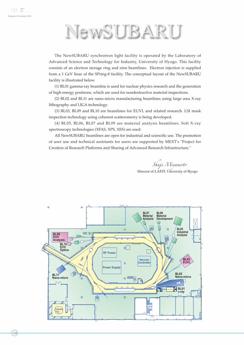
Advanced Science and Technology for Industry, University of Hyogo. This facility consists of an electron storage ring and nine beamlines. Electron injection is supplied from a 1 GeV linac of the SPring-8 facility. The conceptual layout of the NewSUBARU facility is illustrated below.
(1) BL01 gamma-ray beamline is used for nuclear physics research and the generation of high-energy positrons, which are used for nondestructive material inspections.
(2) BL02 and BL11 are nano-micro manufacturing beamlines using large area X-ray lithography and LIGA technology.
(3) BL03, BL09 and BL10 are beamlines for EUVL and related research. LSI mask inspection technology using coherent scatterometry is being developed.
(4) BL05, BL06, BL07 and BL09 are material analysis beamlines. Soft X-ray spectroscopy technologies (XFAS, XPS, XES) are used.
All NewSUBARU beamlines are open for industrial and sciencific use. The promotion of user use and technical assistants for users are supported by MEXT's "Project for Creation of Research Platforms and Sharing of Advanced Research Infrastructure."
Shuji Miyamoto Director of LASTI, University of Hyogo
BL09EUVAnalysis
BL10EUVOptics
BL11Nano-micro
LEENATHz
BL01γ-ray
BL02Nano-micro
BL03EUVL
BL05IndustrialAnalysis
BL06MaterialDevelopment
BL07MaterialAnalysis
VaccumController
RF Power
Power Supply
Research Frontiers 2015Research Frontiers 2015 Research Frontiers 2015Research Frontiers 2015NewSUBARU NewSUBARUResearch Frontiers 2015Research Frontiers 2015 Research Frontiers 2015Research Frontiers 2015Research Frontiers 2015 Research Frontiers 2015
149
Owing to the high brilliance of soft X-ray radiation sources, the study of electronic states by X-ray emission spectroscopy (XES) has recently attracted attention in various research topics such as lithium ion batteries, fuel cells, compound semiconductors, and photocatalysts. Since the penetration depth of soft X-rays is greater than that of electrons, XES is applicable to the electronic state analysis of the bulk and interfacial layers. Because the X-ray emission probability of light elements (Li-F) is low, and decreases with decreasing atomic number [1], an intense excitation light source is necessary for XES measurement. The NewSUBARU synchrotron radiation facility is equipped with a long undulator (LU) with a total length of approximately 11 m [2], and its photon flux density is as high as 1.2×10¹¹ photons/s at the sample position. Therefore, it is suitable as an excitation light source for the XES of light elements.
We have focused on the energy region of 50–600 eV and developed XES equipment with high energy resolution at BL-09A. The optical design of the spectrometer is based on a grazing incidence flat-field spectrometer using a valid line-spacing (VLS) grating. Because there is a limitation of the spatial space, the design concept of the HEPA2.5 (High Efficiency Photon Energy Analyzer Ver.2.5) spectrometer [3], which has relatively high resolution for its small size, was adopted for the optical design of the spectrometer. The entrance slit is placed 10 mm from a sample and its opening width can be changed in the range of 5–300 μm from outside of the vacuum chamber. Taking into account the contribution of the electron cloud on CCD, the energy resolution, E/ΔE, was estimated to be greater
than 1000 in the energy range of 50–600 eV.The spectrometer was constructed at the
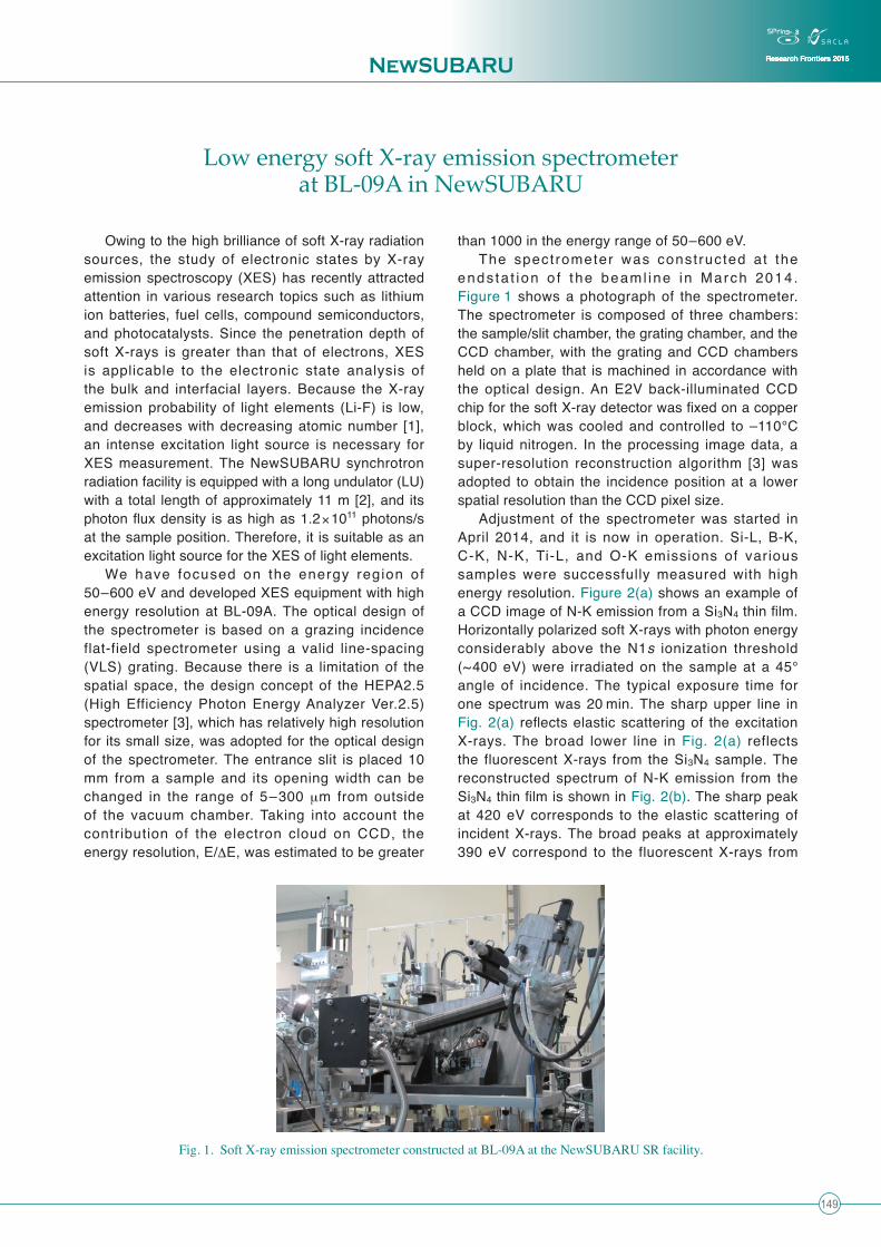
ends ta t ion o f the beaml ine in March 2014 . Figure 1 shows a photograph of the spectrometer. The spectrometer is composed of three chambers: the sample/slit chamber, the grating chamber, and the CCD chamber, with the grating and CCD chambers held on a plate that is machined in accordance with the optical design. An E2V back-illuminated CCD chip for the soft X-ray detector was fixed on a copper block, which was cooled and controlled to –110°C by liquid nitrogen. In the processing image data, a super-resolution reconstruction algorithm [3] was adopted to obtain the incidence position at a lower spatial resolution than the CCD pixel size.
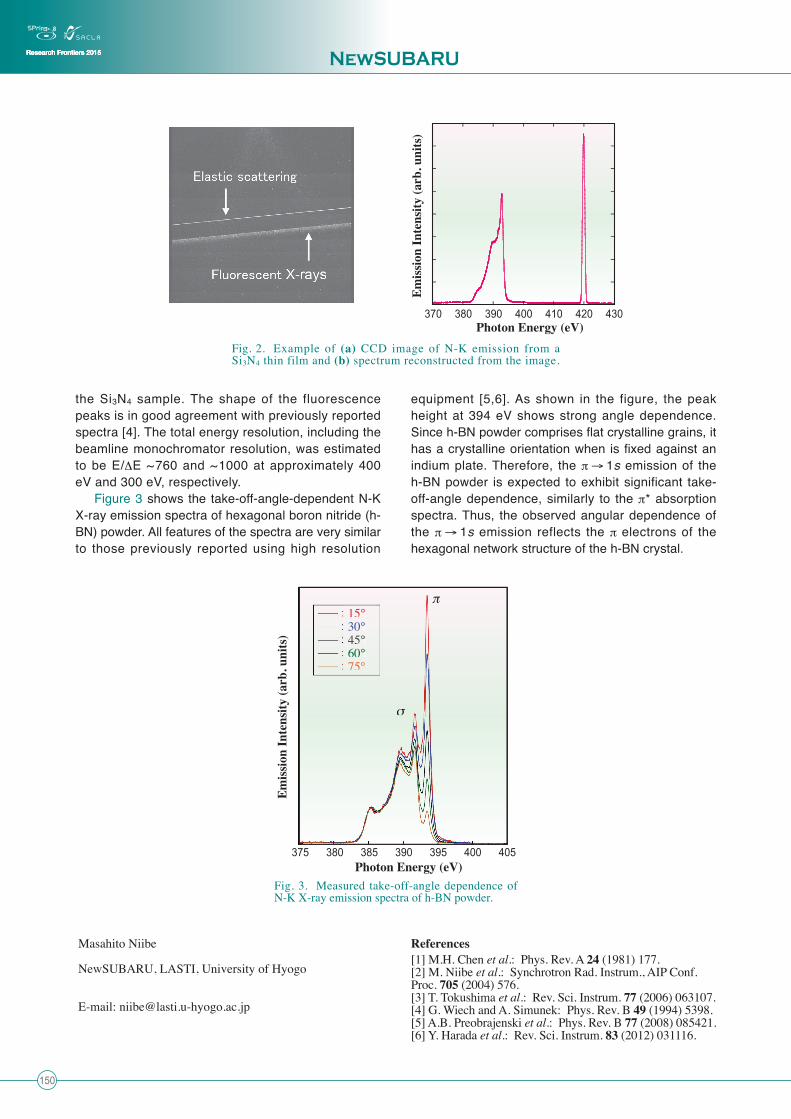
Adjustment of the spectrometer was started in April 2014, and it is now in operation. Si-L, B-K, C-K, N-K, Ti-L, and O-K emissions of various samples were successfully measured with high energy resolution. Figure 2(a) shows an example of a CCD image of N-K emission from a Si3N4 thin film. Horizontally polarized soft X-rays with photon energy considerably above the N1s ionization threshold (~400 eV) were irradiated on the sample at a 45° angle of incidence. The typical exposure time for one spectrum was 20 min. The sharp upper line in Fig. 2(a) reflects elastic scattering of the excitation X-rays. The broad lower line in Fig. 2(a) reflects the fluorescent X-rays from the Si3N4 sample. The reconstructed spectrum of N-K emission from the Si3N4 thin film is shown in Fig. 2(b). The sharp peak at 420 eV corresponds to the elastic scattering of incident X-rays. The broad peaks at approximately 390 eV correspond to the fluorescent X-rays from
Fig. 1. Soft X-ray emission spectrometer constructed at BL-09A at the NewSUBARU SR facility.
Low energy soft X-ray emission spectrometer at BL-09A in NewSUBARU
Research Frontiers 2015Research Frontiers 2015 Research Frontiers 2015Research Frontiers 2015NewSUBARU NewSUBARUResearch Frontiers 2015Research Frontiers 2015 Research Frontiers 2015Research Frontiers 2015
150
the Si3N4 sample. The shape of the fluorescence peaks is in good agreement with previously reported spectra [4]. The total energy resolution, including the beamline monochromator resolution, was estimated to be E/ΔE ~760 and ~1000 at approximately 400 eV and 300 eV, respectively.
Figure 3 shows the take-off-angle-dependent N-K X-ray emission spectra of hexagonal boron nitride (h-BN) powder. All features of the spectra are very similar to those previously reported using high resolution
equipment [5,6]. As shown in the figure, the peak height at 394 eV shows strong angle dependence. Since h-BN powder comprises flat crystalline grains, it has a crystalline orientation when is fixed against an indium plate. Therefore, the π → 1s emission of the h-BN powder is expected to exhibit significant take-off-angle dependence, similarly to the π* absorption spectra. Thus, the observed angular dependence of the π → 1s emission reflects the π electrons of the hexagonal network structure of the h-BN crystal.
Masahito Niibe
NewSUBARU, LASTI, University of Hyogo
E-mail: [email protected]
References[1] M.H. Chen et al.: Phys. Rev. A 24 (1981) 177.[2] M. Niibe et al.: Synchrotron Rad. Instrum., AIP Conf. Proc. 705 (2004) 576. [3] T. Tokushima et al.: Rev. Sci. Instrum. 77 (2006) 063107. [4] G. Wiech and A. Simunek: Phys. Rev. B 49 (1994) 5398.[5] A.B. Preobrajenski et al.: Phys. Rev. B 77 (2008) 085421. [6] Y. Harada et al.: Rev. Sci. Instrum. 83 (2012) 031116.
Fig. 2. Example of (a) CCD image of N-K emission from a Si3N4 thin film and (b) spectrum reconstructed from the image.
Fig. 3. Measured take-off-angle dependence of N-K X-ray emission spectra of h-BN powder.
Photon Energy (eV)
Emiss
ion
Inte
nsity
(arb
. uni
ts)
370 380 390 400 410 420 430
Photon Energy (eV)
Emiss
ion
Inte
nsity
(arb
. uni
ts)
15°30°
60°45°
75°
375 380 385 390 395 400 405
π
σ
15°30°
60°4545°
75°
π
σσ