Embed Size (px)
Citation preview

Research ArticleVision-Augmented Molecular DynamicsSimulation of Nanoindentation
Rajab Al-Sayegh and Charalampos Makatsoris
Department of Mechanical, Aerospace and Civil Engineering, College of Engineering, Design and Physical Sciences,Brunel University London, Kingston Lane, Uxbridge UB8 3PH, UK
Correspondence should be addressed to Charalampos Makatsoris; [email protected]
Received 15 December 2014; Revised 14 April 2015; Accepted 16 April 2015
Academic Editor: Nadimul Faisal
Copyright © 2015 R. Al-Sayegh and C. Makatsoris. This is an open access article distributed under the Creative CommonsAttribution License, which permits unrestricted use, distribution, and reproduction in any medium, provided the original work isproperly cited.
We present a user-friendly vision-augmented technique to carry out atomic simulation using hand gestures. The system is novelin its concept as it enables the user to directly manipulate the atomic structures on the screen, in 3D space using hand gestures,allowing the exploration and visualisation of molecular interactions at different relative conformations.The hand gestures are usedto pick and place atoms on the screen allowing thereby the ease of carrying out molecular dynamics simulation in a more efficientway.The end result is that users with limited expertise in developingmolecular structures can now do so easily and intuitively by theuse of body gestures to interact with the simulator to study the system in question. The proposed system was tested by simulatingthe crystal anisotropy of crystalline silicon during nanoindentation. A long-range (Screened bond order) Tersoff potential energyfunction was used during the simulation which revealed the value of hardness and elastic modulus being similar to what has beenfound previously from the experiments. We anticipate that our proposed system will open up new horizons to the current methodson how an MD simulation is designed and executed.
1. Introduction
Computational simulation approaches, such as moleculardynamics (MD), Monte Carlo, or coarse grained MD, arewidely employed by chemists and materials scientists topredict and understand the behaviour of materials. Theseapproaches have a high computational cost as they tend toget confined within local regions of the energy landscapespending many CPU during a simulation run. This researchis focused on the development of a virtual environmentwhich offers an entirely new way to explore complex energylandscapes by allowing the user to directly interact with thesimulated molecular system [1]. Our approach entails the useof computer vision and specifically gesture recognition toenable the user to interact with the simulated system exploit-ing the numerous degrees of freedom available with handgestures in 3D space, breaking away from the constraintsof traditional methods of interaction involving a high levellanguage based inputs which became the motivation for thispaper.This approach progresses the current state of the art viaa step change in understanding of the complex interactions
as well as allowing the rapid design of novel molecular struc-tures using an intuitive way of interaction with a simulatorby means of hand gestures. We demonstrate our approachand describe our vision-augmented molecular dynamicssimulation (VAMDS) system on the nanoindentation of asilicon crystal silicon substrate. The paper is organised asfollows. Section 2 briefly reviews earlier efforts in designand simulation systems driven by haptic devices. Section 3presents our proposed VAMDS methodology. In Section 4,the nanoindentation study using the VAMDS system isdescribed. Finally in Section 5, we conclude by presenting thesimulation results obtained from the system exploring crystalanisotropy of silicon during its nanoindentation.
2. Literature Review
The work in this paper was especially inspired from thepioneering work of Mistry et al. [2] at MIT, in an attemptto help the disabled people produced a wearable gestureinterface using a small camera and a projector. The purpose
Hindawi Publishing CorporationJournal of NanomaterialsVolume 2015, Article ID 857574, 11 pageshttp://dx.doi.org/10.1155/2015/857574
2 Journal of Nanomaterials
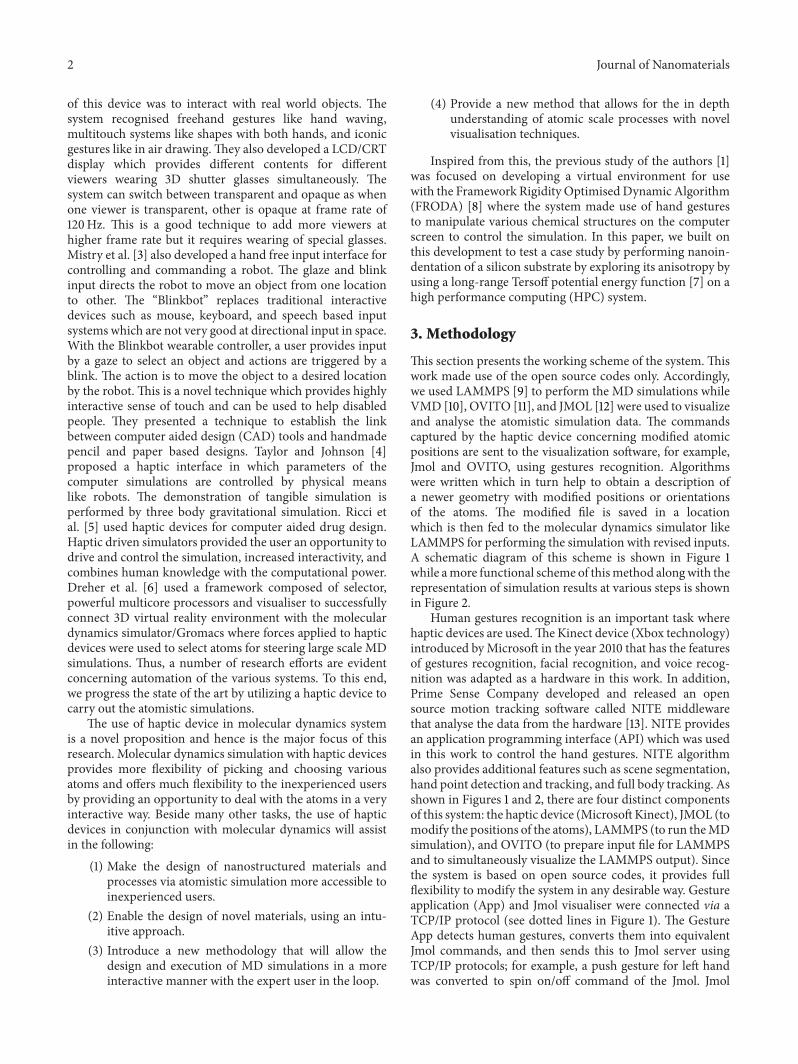
of this device was to interact with real world objects. Thesystem recognised freehand gestures like hand waving,multitouch systems like shapes with both hands, and iconicgestures like in air drawing.They also developed a LCD/CRTdisplay which provides different contents for differentviewers wearing 3D shutter glasses simultaneously. Thesystem can switch between transparent and opaque as whenone viewer is transparent, other is opaque at frame rate of120Hz. This is a good technique to add more viewers athigher frame rate but it requires wearing of special glasses.Mistry et al. [3] also developed a hand free input interface forcontrolling and commanding a robot. The glaze and blinkinput directs the robot to move an object from one locationto other. The “Blinkbot” replaces traditional interactivedevices such as mouse, keyboard, and speech based inputsystems which are not very good at directional input in space.With the Blinkbot wearable controller, a user provides inputby a gaze to select an object and actions are triggered by ablink. The action is to move the object to a desired locationby the robot. This is a novel technique which provides highlyinteractive sense of touch and can be used to help disabledpeople. They presented a technique to establish the linkbetween computer aided design (CAD) tools and handmadepencil and paper based designs. Taylor and Johnson [4]proposed a haptic interface in which parameters of thecomputer simulations are controlled by physical meanslike robots. The demonstration of tangible simulation isperformed by three body gravitational simulation. Ricci etal. [5] used haptic devices for computer aided drug design.Haptic driven simulators provided the user an opportunity todrive and control the simulation, increased interactivity, andcombines human knowledge with the computational power.Dreher et al. [6] used a framework composed of selector,powerful multicore processors and visualiser to successfullyconnect 3D virtual reality environment with the moleculardynamics simulator/Gromacs where forces applied to hapticdevices were used to select atoms for steering large scale MDsimulations. Thus, a number of research efforts are evidentconcerning automation of the various systems. To this end,we progress the state of the art by utilizing a haptic device tocarry out the atomistic simulations.
The use of haptic device in molecular dynamics systemis a novel proposition and hence is the major focus of thisresearch. Molecular dynamics simulation with haptic devicesprovides more flexibility of picking and choosing variousatoms and offers much flexibility to the inexperienced usersby providing an opportunity to deal with the atoms in a veryinteractive way. Beside many other tasks, the use of hapticdevices in conjunction with molecular dynamics will assistin the following:
(1) Make the design of nanostructured materials andprocesses via atomistic simulation more accessible toinexperienced users.
(2) Enable the design of novel materials, using an intu-itive approach.
(3) Introduce a new methodology that will allow thedesign and execution of MD simulations in a moreinteractive manner with the expert user in the loop.
(4) Provide a new method that allows for the in depthunderstanding of atomic scale processes with novelvisualisation techniques.
Inspired from this, the previous study of the authors [1]was focused on developing a virtual environment for usewith the Framework Rigidity OptimisedDynamic Algorithm(FRODA) [8] where the system made use of hand gesturesto manipulate various chemical structures on the computerscreen to control the simulation. In this paper, we built onthis development to test a case study by performing nanoin-dentation of a silicon substrate by exploring its anisotropy byusing a long-range Tersoff potential energy function [7] on ahigh performance computing (HPC) system.
3. Methodology
This section presents the working scheme of the system.Thiswork made use of the open source codes only. Accordingly,we used LAMMPS [9] to perform the MD simulations whileVMD [10], OVITO [11], and JMOL [12] were used to visualizeand analyse the atomistic simulation data. The commandscaptured by the haptic device concerning modified atomicpositions are sent to the visualization software, for example,Jmol and OVITO, using gestures recognition. Algorithmswere written which in turn help to obtain a description ofa newer geometry with modified positions or orientationsof the atoms. The modified file is saved in a locationwhich is then fed to the molecular dynamics simulator likeLAMMPS for performing the simulation with revised inputs.A schematic diagram of this scheme is shown in Figure 1while amore functional scheme of thismethod alongwith therepresentation of simulation results at various steps is shownin Figure 2.
Human gestures recognition is an important task wherehaptic devices are used.TheKinect device (Xbox technology)introduced byMicrosoft in the year 2010 that has the featuresof gestures recognition, facial recognition, and voice recog-nition was adapted as a hardware in this work. In addition,Prime Sense Company developed and released an opensource motion tracking software called NITE middlewarethat analyse the data from the hardware [13]. NITE providesan application programming interface (API) which was usedin this work to control the hand gestures. NITE algorithmalso provides additional features such as scene segmentation,hand point detection and tracking, and full body tracking. Asshown in Figures 1 and 2, there are four distinct componentsof this system: the haptic device (MicrosoftKinect), JMOL (tomodify the positions of the atoms), LAMMPS (to run theMDsimulation), and OVITO (to prepare input file for LAMMPSand to simultaneously visualize the LAMMPS output). Sincethe system is based on open source codes, it provides fullflexibility to modify the system in any desirable way. Gestureapplication (App) and Jmol visualiser were connected via aTCP/IP protocol (see dotted lines in Figure 1). The GestureApp detects human gestures, converts them into equivalentJmol commands, and then sends this to Jmol server usingTCP/IP protocols; for example, a push gesture for left handwas converted to spin on/off command of the Jmol. Jmol

Journal of Nanomaterials 3
Network connectionCommands/data
The hardwaredevice
gesturesrecognition
TCP/IPconnection
establishment
Gestures
Gestures app
Gestures to Jmolcommandsconversion
Start simulationcommand
Jmolcommands
.dump
.data
Run LAMMPS
Cluster.in
Visualizing
OVITO
Convertingoperation
Jmol server withTCP/IP port
Jmol visualizer
.xyz
Figure 1: Vision-augmented molecular dynamics simulation.
Computer vision/haptic device/gestures app LAMMPS/molecular dynamics/indentation
TCP/IP protocolClient-server architecture (client)
Gesturesapplications
Gesturecommands to
Jmol
OpenNI
NITE middlewarecomponents,for example,
hand gesturestracking
3D depth sensorsRGB camera
Multi-array mic Motorised tilt
Port 3000
ControllingJmol
application
OpenNIinterfaces
Hardwaredevice
(sensor)
Jmolvisualizer(server)
Structuremanipulation
OVITO application toprepare Jmol output for
LAMMPS
Dat
afo
rmat
Dum
pfo
rmat
The potentialfile (.in) Cluster
LAMMPS(molecular dynamics simulator)
XYZ format
Figure 2: Integration between computer vision and molecular dynamics simulation.

4 Journal of Nanomaterials
Step 7: data file is processed by the cluster using LAMMPS engine and results are generated
Step 6: OVITO performs the necessary conversion of XYZ format to the LAMMPS data file
Step 4: manipulate the desirable position of atoms within the molecule using different gestures
Step 3: initiate the gesture app by using the wave gesture
Step 2: load a molecule in XYZ format using Jmol visualizer
Step 1: start the gesture app, the Jmol visualizer, and the OVITO application(the connection is established between the gesture app and the Jmol visualizer via TCP/IP protocols)
Step 5: save the atomic positions in a new xyz file using the circle gesture
Figure 3: Flowchart of the VAMD developed in this work.
server receives this spin on/off command and performsthe spin operation on the atomic structure of the material.Subsequently, OVITO was used to convert XYZ file format(output of Jmol) to the LAMMPS data file format which wassent to HCP server.
The entire process was automated so that the HPC servercan call the LAMMPS engine to generate the simulationoutput in the form of a trajectory at the desired time steps.The output files obtained from LAMMPS were programmedto save in the local computer from the HPC server and theprocess continues until the whole directory containing theLAMMPS output is copied to the local computer. This cyclecontinues while in the meantime, OVITO interactively makethe use visualise each file copied from the HPC server tothe local computer. Briefly, the vision-augmented moleculardynamics simulation developed in this work is comprised ofthe key steps shown in Figure 3.
3.1. Gestures to Jmol Command Conversion. Since we intendto manipulate the position of atoms merely using gestures,we need to convert the gestures into appropriate JMOL com-mands. Some of these conversions are tabulated in Table 1. Inorder to send the JMOL command to the JMOL Visualizer,we use aWireshark tool to capture the data on TCP/IP port toidentify the exact structure of the command. As an example,in order to send the command zoom in, we need to executemovement Swipe left (left hand) and Swipe right (right hand)in front of haptic device. Gesture application will convert thisto the Jmol command format which is “zoom in” and send itto Jmol server via TCP/IP port to do the operation “zoom in”to the molecular structure visualised on Jmol.
We prepare this string for each command and send it overTCP/IP to the JMOL Visualizer. Once the string is receivedby the JMOL server, it executes a particular command and
Table 1: Gestures to JMOL command mapping.
S/number Hand gestures Jmol commands
1 Push (right hand) Left mouse buttonclick
2 Swipe right (righthand)
Right button mouseclick
3 Swipe left (right hand) Set picking dragmolecule
4 Swipe up (right hand) Set picking drag atom
5 Swipe down (righthand) Set picking drag bond
6Swipe right (lefthand) and Swipe left(right hand)
Zoom out
7Swipe left (left hand)and Swipe right (righthand)
Zoom in
8 Swipe up (left hand) Set picking deleteatom
9 Swipe down (lefthand)
Set picking deletebond
10 Push (left hand) Spin on/off
11 Circle (right hand)
Write the output fromJmol in𝑋𝑌𝑍 formatand send this toOVITO
the respective action is taken accordingly. As an example,in the above case, the loaded molecule gets zoomed in. Forother commands, we just replace the zoom in field with thecorresponding JMOL command.

Journal of Nanomaterials 5
Table 2: Details used for the development of MD simulation model.
Dimensions of the silicon workpiece Crystal orientation of silicon Number of atoms16.296 nm × 10.864 nm × 16.296 nm (010) 14400015.9667 nm × 10.7548 nm × 15.9667 nm (110) 13708815.9667 nm × 11.29 nm × 16.132 nm (111) 145152Equilibrium parameters Silicon: 5.432 A and Diamond: 3.5656 AIndenter and specimen surfacedistance 1 nm
Depth of indentation 2 nmSpeed of indentation and retraction 20m/s = 0.02 nm/psDiameter of the indenter 4 nmBoundary conditions Periodic in𝑋 and 𝑍 directionPotential function used Screening bond order Tersoff potential function [7]
� = 20m/s4nm
Indenter
Newton atomsFixed atomsThermostatic atoms
x
y
z
Silicon substrate(010) orientation
10.86 nm
16.296nm16.296nm
Figure 4: Schematic of the MD simulation.
4. MD Simulation of the Nanoindentation ofCrystalline Silicon with VAMDS
4.1. MD Simulation Methodology. In this section we demon-strate the methodology adopted for simulating nanoinden-tation of silicon using VAMDS. The aim of the study wasto explore the crystal anisotropy of silicon in such a waythat the orientation of the crystal can be switched merelyby the hand gestures. To this end, the simulation modelwas first developed by following the standard algorithm,boundary conditions, and ensemble in the same way as hasbeen previously done in other research papers [14–16]. Aschematic simulation model used to carry out the simulationis shown in Figure 4. In Figure 4, the atoms in the indenterwere kept fixed (diamond indenter was assumed to be aninfinite rigid body structure) and, in the three test cases, thecrystal orientation of silicon was varied. Goel et al. [14] haveprovided a glance of other research works where a highervelocity (up to 500m/s) has been frequently used to overcomethe limitations of MD simulation. To achieve more realisticresults, we made use of an indentation velocity of 20m/s
as has been recently used on HPC systems [17]. Also, wemade use of long-range Tersoff potential energy function [7]for describing silicon and carbon as it provides improveddescription of silicon.
The details of the parameters used to develop the MDsimulation model are shown in Table 2. In the MD simu-lation model, to avoid any artificial effect of the tempera-ture (due to thermal fluctuations and thermal vibrations),a low temperature of 10 K was used to equilibrate thesample and perform the nanoindentation. During the MDsimulation, the atomic stress tensor (http://lammps.sandia.gov/doc/compute stress atom.html) was calculated by con-sidering an elemental atomic volume (1 nm × 1 nm × 1 nm) ofsilicon in the deformation zone right underneath the inden-ter.
In addition to stress calculation, further analysis was car-ried out by estimating the contact pressure (𝑝
𝑚) underneath
the indenter. Contact pressure (𝑝𝑚) is defined as the ratio of
the instantaneous normal force (𝐹) on the indenter and theprojected area (𝐴) which is calculated as (2𝜋 × 𝑎 × ℎ) for aspherical indenterwhere𝑎 = √ℎ(2𝑅 − ℎ) is the contact radiusof the spherical indenter,𝑅 is the radius of the indenter, and ℎis the instantaneous displacement of the indenter.The averagevalue of the contact pressure (after it attains saturation value)is also referred to as nanoindentation hardness (𝐻) of thematerial.
A popular way of calculation of the elastic modulus (𝐸𝑠)
and hardness (𝐻) of the material from the load-displacement(𝑃-ℎ) plot was proposed by Oliver and Pharr [18] during thelast decade of 20th century.Theirmethod relies on calculationof the projected contact area by drawing an imaginary line,typically following the power law, on the top 1/3rd part alongthe unloading curve of the 𝑃-ℎ plot. The slope of this curve(𝑆) thus enables to obtain the reduced elastic modulus ofthe material which can then be used to obtain 𝐸
𝑠(elastic
modulus) of the specimen using the following equations:
𝐸𝑟=1
𝛽
√𝜋
2
𝑆
√𝐴
,
1 − 𝜐𝑠
2
𝐸𝑠
=1
𝐸𝑟
−1 − 𝜐𝑖
2
𝐸𝑖
.
(1)

6 Journal of Nanomaterials
In (1), 𝐸𝑟is the reduced elastic modulus (N/m2), 𝑆 is the
slope of the top 1/3rd part of the unloading curve whichwere obtained as 729N/m (for (010) oriented Si), 820N/m(for (110) oriented Si), and 914N/m (for (111) oriented Si)from the simulation results, 𝛽 = 1 is a constant for sphericalindenter, and 𝐴 is the projected area (m2) which varies withthe depth of indentation. For accuracy of computation of𝐸𝑠, other parameters such as 𝜐
𝑠= 0.3459 (Poisson’s ratio of
silicon), 𝜐𝑖= 0.103 (Poisson’s ratio of Diamond), and 𝐸
𝑖=
1056.48GPa (Young’s modulus of diamond) were obtaineddirectly from the potential function.
4.2. MD Simulation Results
4.2.1. Calibration of the Gesture Application with the MDSimulation Model. Figure 5 shows the progressive physi-cal movement of the human hand sensed by the gestureapplication (left column) and transformation of this physicalhand movement into the corresponding displacement of theindenter into the substrate (right hand column).The physicaldistances of the hand movements were captured through ameasurement tape and were compared with the movementof the indenter in the MD simulation model so as to seethe factor by which the hand movement transfers into theequivalent displacement of the indenter.The relation betweenthese two movements was plotted and is shown in Figure 6.Knowing this relation was a preliminary step for calibratingthe newly proposed VAMDS system.
4.2.2. HPPT of Silicon and Extraction of the Mechanical Prop-erties fromP-h Plot. Theductile behaviour of brittlematerialsis often attributed to an event recognized as high-pressurephase transformation (HPPT). HPPT enforces brittle mate-rials to become ductile for the short duration of loadingwhich upon unloading eventually transforms to amorphousphase of the brittle material. HPPT of silicon during itsnanoindentation has been explained to be driven from thedeviatoric stress rather than temperature [14] in the deforma-tion zone. Much of the literature on silicon nanoindentationhave reportedHPPT to be the primarymechanism governingthe plasticity of silicon that causes brittle-ductile transition.There is however a noticeable exception of Mylvaganamand Zhang [19] observed nanotwinning (associated with Si-I to bct-5 phase transformation) in silicon along the ⟨110⟩direction that stops at Shockley partial dislocation. It wastherefore relevant to assert the occurrence of HPPT in thiswork for which an indicator known as coordination numberwas used for its ease of implementation.
A snapshot from the MD simulation showing the changein coordination number during peak loading of silicon onvarious orientations is shown in Figure 7. The coordinationnumber of 4 (Figure 7) is representative of bulk siliconwhile coordination number of 1 and 2 on the free surface ofsilicon workpiece represents the dangling bonds on the Si-terminated nascent surface. During the nanoindentation, thecoordination number in the indentation zone was observedto change from 4 to 6 with a corresponding change in thenumber of nearest neighbour atoms. Literature suggests that
this change corresponds to an allotropic transformation of sil-icon from the diamond cubic (alpha-silicon) to the body cen-tred tetragonal (beta-silicon) structure and is consistent withthe previously reported results of Si-I to Si-II during loading.Most of the metastable phases of silicon were observed toform along the ⟨110⟩ direction, which is the direction of slipplane in silicon [20] as is shown in Figure 7 while the (111)planes act as both slip planes and cleavage planes.
Figure 8 is a 𝑃-ℎ plot obtained from the displacementcontrolled nanoindentation simulation where the penetra-tion depth of the diamond tool was kept fixed at 2 nm. Aninteresting observation concerning the 𝑃-ℎ plot comes fromthe work of Jang et al. [21] where a good correlation betweenunloading curve and the phase of the material formedpostindentation of silicon was observed. Based on the micro-Raman spectra, the authors proposed that the unloadingdiscontinuity, often called as “pop-out,” corresponds to theformation ofmetastable Si-XII/Si-III crystalline phases, whilethe hysteresis, called the “elbow” is associated with theformation of a-Si. In Figure 8, an interesting feature observedfrom the 𝑃-ℎ plot was that the unloading curve for the(110) and the (111) substrate followed power law whereas theunloading curve on the (010) substrate showed an elbow.Thischaracteristic is a testimony to the formation of a-Si upon theretraction of the indenter on the (010) orientation.
Another interesting feature observed from the 𝑃-ℎ plotobtained from the MD simulation was the residual indenta-tion depth (ℎ
𝑓) that can also be used to characterize the recov-
ery of the indented surface upon retraction of the indenter. Inthis case, ℎ
𝑓was quantified from the 𝑃-ℎ plot (Figure 8) for
all the three simulated orientations and was found inevitablydifferent in all the cases; that is, ℎ
𝑓(010) was minimum
while ℎ𝑓for the (111) orientation was maximum whereas ℎ
𝑓
(110) was intermittent. This suggests that at atomic scale, the(010) orientation will show higher extent of elastic recoverythan the (111) orientation of silicon. This result is somewhatconsistent with the earlier work of Shibata et al. [22] wherea Schmidt-type slip orientation factor was proposed and the⟨110⟩ direction either on the (100) or on the (111) planeswas recognized as more preferred combination to plasticallydeform the silicon. Lastly, beside a monotonic increase in theloading curve, a strong cohesion between the indenter andthe substrate during retraction was also observed.
HPPT is highly direction sensitive [23, 24]; that is,pressure or hydrostatic stress required for transformation onthe (111) orientation is lower than that required to inducethe transformation on the (100) orientation [20]. Literaturesuggests that the transformation pressure required to causemetallisation of silicon varies between 9 and 18GPa [25]. Itmay however be noted that the hydrostatic pressure differsfrom deviatoric stress [26]. During nanoindentation, siliconundergoes both shear and compression making it differentfrom the case of simple compressive pressure.
As it can be seen from Table 3, the hydrostatic stress(pressure) [27] in the indentation zone was observed tobe maximum on the (110) orientation followed by (010)orientation and it wasminimum for the (111) orientation.Thiscorrelation was however not the same for the vonMises stressand Tresca stress in the indentation zone.

Journal of Nanomaterials 7
(010) orientation
(100)
(010)
(001)
130 cm
Surface atoms
Diamondindenter
Common neighbour analysis of the silicon substrate
Physical movement of the hand gesture Common neighbour analysis of the silicon substrate
(a)
(010) orientation
124 cm
(b)
(010) orientation
110 cm
Phase transformation
(c)
Figure 5: Comparison of physical movement with the movement in the MD simulation model (a) at the beginning of the simulation, (b)when the indenter establishes contact with the substrate and (c) final indentation depth was achieved.
For the two kinds of deviatoric stresses, the (110) orienta-tion showed maximum values whereas the (010) orientationshowed least value. The peak average temperature in thecutting zone was rather high, especially considering the factthat nanoindentation process was carried out at 10 K. At its
peak, the (111) orientation showed themaximum temperatureof about 438K followed by the (110) orientation at 419 Kwhereas the (010) orientation showed the least temperature of300K. Finally, the elasticmoduluswas obtained from𝑃-ℎplotusing Oliver and Pharr method and accordingly the variation

8 Journal of Nanomaterials
Table 3: Computational results obtained from the nanoindentation simulation.
Silicon (010) orientation (110) orientation (111) orientationAverage hardness (GPa) at indentdepth of 2 nm 16.99 18.22 18.48
Elastic modulus (GPa) at indentdepth of 2 nm 129 147 167
ℎ𝑓/ℎmax (extent of elastic
recovery)1.17/2=0.585
1.36/2=0.68
1.47/2=0.735
Peak maximum von Mises stressin the indent zone (GPa) 11.07 22.75 16.72
Peak maximum Tresca stress inthe indent zone (GPa) 5.91 12.11 9.14
Peak maximum octahedral shearstress in the indent zone (GPa) 5.21 10.72 7.88
Peak hydrostatic stress in theindent zone (GPa) 20.11 21.98 16.62
Peak temperature in theindentation zone (K) 300 419 438
Features of the 𝑃-ℎ curve duringunloading
Elbow formationcorresponding toa-Si formation
No feature No feature
Mov
emen
t of t
he in
dent
er (n
m)
Movement of hand (cm)
3.5
3.0
2.5
2.0
1.5
1.0
0.5
0.0
−0.5
0 5 10 15 20
Experimentally measured movement of the indenterTheoretical movement of the indenter
Figure 6: Relationship between physical movement of hand gestureand indenter in the MDmodel.
in𝐸 and hardness on all the three crystal surfaces with respectto change in the indentation depth is plotted and shown inFigure 9.
It is interesting to note from Figure 9(a) that the elasticmodulus at finite indentation depth of few nanometresdecrease sharply until attaining a saturated value as theindentation depth increases. At an indentation depth of 2 nm,the elastic modulus of the three simulated orientations wasobtained as 129GPa for the (010) orientation, 147GPa for the(110) orientation, and 167GPa for the (111) orientation. Thesevalues are well comparable with the experimental values ofthe elastic modulus of silicon [28, 29] and resembles similarto what has been obtained fromMD [30].
It has been seen how a new approach is helpful incarrying out atomic simulations. Future work of this researchwill realise multiscale approach by integrating computervision (e.g., gesture recognition and artificial intelligence),molecular dynamics (e.g., molecular modelling and materialmodelling), and intuitive understating of atomic scale. Bydoing this, we will be able to interact with molecules via oursenses.
5. Conclusions
This work was aimed at developing a vision-augmentedmolecular dynamics simulation (VAMDS) method whichwas tested by performing a case study on nanoindentation ofsilicon. It was remarkably challenging yet innovative becauseit will open up new horizons for the development of newknowledge by building a clear base to enable design andcreation of novel materials. This was achieved through asystematic design approach integrating the use of a hapticdevice that fed the data of hand gestures to the simulator.Aside from explaining various aspects of the hardware,design, anddevelopment of this vision-augmented technique,the following points can be concluded based on the afore-mentioned discussions:
(1) The mechanism of ductility in silicon during itsnanoindentation and the observed plasticity occursdue to the high pressure phase transformation(HPPT) that is driven by stress rather than tem-perature. For HPPT to occur in silicon, the vonMises and Tresca stress for the (110) orientation werefound maximum while the (010) orientation showedthe least values whereas the (111) orientation showedsomewhat an intermittent value.

Journal of Nanomaterials 9
(010) orientation
(100)
(010)
(001)
(110) orientation
6
1
Coo
rdin
atio
n nu
mbe
r
6
1C
oord
inat
ion
num
ber
6
1
Coo
rdin
atio
n nu
mbe
r
(−11−2)
(110)
(1−1−1)
(111) orientation
(01−1)
(111)
(−211)
Figure 7: Change in coordination number at peak indentation depth of 2 nm on three orientations.
450
400
350
300
250
200
150
100
50
0
−50
−100
−150
0.0
0.2
0.4
0.6
0.8
1.0
1.2
1.4
1.6
1.8
2.0
2.2
2.4
2.6
2.8
3.0
3.2
Displacement (nm)
Inde
ntat
ion
forc
e (nN
)
(010) orientation(110) orientation(111) orientation
Depth of indenter by 3nm correspondsto 20 cm of hand movement
Free travel Depth of indentation(0,0)
Loading Unloading
Elbow
hf
hf(010) = 2.17 − 1 = 1.17nmhf(110) = 2.36 − 1 = 1.36nmhf(111) = 2.47 − 1 = 1.47nm
Figure 8: 𝑃-ℎ plots of the nanoindentation for all three crystalorientations of silicon.
(2) At an indentation depth of 2 nm, it was seen that theunloading curve for the (110) and the (111) substratefollows power law whereas the unloading curve on
the (010) substrate showed an elbow which was foundrelated with the formation of a-Si upon the retractionof the indenter on the (010) orientation only. Fur-thermore, the elastic constants of silicon varied in theorder of 𝐸
111> 𝐸110> 𝐸010
.
(3) Obtaining the variation in the hardness and elasticmodulus using classical way of doing moleculardynamics simulation would have been a relativelytedious task but, with the implementation of theVAMD, this is easily achievable. The use of hapticdevice as shown in this work reduces the pain ofobtaining mechanical property via 𝑃-ℎ profile as thesimulation run can be restarted fromany pointmerelyby the use of hand gestures which is themajor noveltyof this work.
Abbreviations
NITE: Natural interaction for end-userFRODA: Framework Rigidity Optimised Dynamic
AlgorithmHPC: High performance computingJMOL: Java viewer for molecules in 3D

10 Journal of Nanomaterials
500
450
400
350
300
250
200
150
100
0.5
0.6
0.7
0.8
0.9
1.0
1.1
1.2
1.3
1.4
1.5
1.6
1.7
1.8
1.9
2.0
Varia
tion
in th
e val
ue o
fE(G
Pa)
Indentation depth (nm)Variation in E of silicon on the (010) orientationVariation in E of silicon on the (110) orientationVariation in E of silicon on the (111) orientation
∼167GPa∼147GPa∼129GPa
(a)
30
25
20
15
10
5
0.0 0.5 1.0 1.5 2.0
Indentation depth (nm)
Nan
oind
enta
tion
hard
ness
(GPa
)
Hardness (010)Hardness (110)Hardness (111)
Unstable hardnessRegion of stable nanoindentation hardness
Change in the nanoindentationhardness with crystal orientation
values
(b)
Figure 9: Variation in the (a) elastic modulus and (b) nanoindentation hardness of silicon with respect to the indentation depth.
GestureApp: Application which convert gestures tocommands
MD: Molecular dynamicsNVE: Microcanonical ensembleOVITO: Open visualization toolPBC: Periodic boundary conditionTEM: Transmission electron microscopeVAMDS: Vision-augmented molecular dynam-
ics simulationVMD: Visual molecular dynamics.
Nomenclatures
𝑎: Contact radius of the spherical indenter𝐴: Projected area𝐵: Bulk modulus𝐶𝑖𝑗: Elastic constants of the material𝐸 or 𝐸
𝑠: Elastic modulus of the material
𝐹 or 𝑃: Normal force or load on the indenter𝐺: Shear modulusℎ: Instantaneous displacement of the
indenterℎ𝑓: Residual depth of indentationℎmax: Maximum depth of indentation𝐻: Hardness of the material𝐾: Force constant𝑃-ℎ: Load-displacement curve𝑝𝑚: Contact pressure𝑅: Radius of the indenter𝑟0: Cutoff radius between indenter and the
substrate material𝑆: Slope of the unloading curve𝜎hydrostatic: Hydrostatic stress𝜎1, 𝜎2, and 𝜎
3: Principal stresses
𝜀: Strain𝜏: Shear stress.
Conflict of Interests
The authors declare that there is no conflict of interestsregarding the publication of this paper.
Acknowledgments
Authors acknowledge the funding support of King Abdullahbin Abdul-Aziz Al-Saud, Ministry of Higher Education, andNorthern Borders University, Kingdom of Saudi Arabia, forfunding the Ph.D. of the first author.
References
[1] R. Alsayegh, L. Paramonov, and C. Makatsoris, “A novel virtualenvironment for molecular system design,” in Proceedings ofthe IEEE International Conference on Computational Intelligenceand Virtual Environments for Measurement Systems and Appli-cations (CIVEMSA ’13), pp. 37–42, July 2013.
[2] P. Mistry, P. Maes, and L. Chang, “WUW—wear Ur world: awearable gestural interface,” in Proceedings of the 27th Inter-national Conference Extended Abstracts on Human Factors inComputing Systems (CHI ’09), pp. 4111–4116, ACM, Boston,Mass, USA, April 2009.
[3] P. Mistry, K. Ishii, M. Inami, and T. Igarashi, “Blinkbot: lookat, blink and move,” in Proceedings of the 23nd Annual ACMSymposium on User Interface Software and Technology, ACM,2010.
[4] T. Taylor and D. E. Johnson, “Tangible simulations generalizedhaptic devices for human-guided computer simulations,” inProceedings of the International Conference on CollaborationTechnologies and Systems (CTS ’13), San Diego, Calif, USA, May2013.
[5] A. Ricci, A. Anthopoulos, A. Massarotti, I. Grimstead, and A.Brancale, “Haptic-driven applications to molecular modeling:state-of-the-art and perspectives,” Future Medicinal Chemistry,vol. 4, no. 10, pp. 1219–1228, 2012.

Journal of Nanomaterials 11
[6] M. Dreher, M. Piuzzi, A. Turki et al., “Interactive moleculardynamics: scaling up to large systems,” Procedia ComputerScience, vol. 18, pp. 20–29, 2013.
[7] L. Pastewka, A. Klemenz, P. Gumbsch, and M. Moseler,“Screened empirical bond-order potentials for Si-C,” PhysicalReview B, vol. 87, no. 20, Article ID 205410, 12 pages, 2013.
[8] S. Wells, S. Menor, B. Hespenheide, and M. F. Thorpe, “Con-strained geometric simulation of diffusive motion in proteins,”Physical Biology, vol. 2, no. 4, pp. S127–S136, 2005.
[9] S. Plimpton, “Fast parallel algorithms for short-rangemoleculardynamics,” Journal of Computational Physics, vol. 117, no. 1, pp.1–19, 1995.
[10] W. Humphrey, A. Dalke, and K. Schulten, “VMD: visualmolecular dynamics,” Journal of Molecular Graphics, vol. 14, no.1, pp. 33–38, 1996.
[11] A. Stukowski, “Visualization and analysis of atomistic simula-tion data with OVITO—the Open Visualization Tool,” Mod-elling and Simulation in Materials Science and Engineering, vol.18, no. 1, Article ID 015012, 2010.
[12] September 2014, http://jmol.sourceforge.net/docs/JmolUserGu-ide/ch04.html.
[13] PrimeSense, NITE Controls User Guide, Primesense Inc, 2011.[14] S. Goel, N. H. Faisal, X. Luo, J. Yan, and A. Agrawal, “Nanoin-
dentation of polysilicon and single crystal silicon: moleculardynamics simulation and experimental validation,” Journal ofPhysics D: Applied Physics, vol. 47, no. 27, Article ID 275304,2014.
[15] S. Goel, A. Agrawal, and N. H. Faisal, “Can a carbon nano-coating resist metallic phase transformation in silicon substrateduring nanoimpact?”Wear, vol. 315, no. 1-2, pp. 38–41, 2014.
[16] S. Goel, S. S. Joshi, G. Abdelal, and A. Agrawal, “Moleculardynamics simulation of nanoindentation of Fe3C and Fe4C,”Materials Science and Engineering A, vol. 597, pp. 331–341, 2014.
[17] L. Pastewka, S. Moser, P. Gumbsch, and M. Moseler, “Ani-sotropic mechanical amorphization drives wear in diamond,”Nature Materials, vol. 10, no. 1, pp. 34–38, 2011.
[18] W. C. Oliver and G. M. Pharr, “An improved technique fordetermining hardness and elastic modulus using load anddisplacement sensing indentation experiments,” Journal ofMaterials Research, vol. 7, no. 6, pp. 1564–1580, 1992.
[19] K. Mylvaganam and L. C. Zhang, “Nanotwinning in monocrys-talline silicon upon nanoscratching,” Scripta Materialia, vol. 65,no. 3, pp. 214–216, 2011.
[20] D. E. Kim and S. I. Oh, “Atomistic simulation of structuralphase transformations in monocrystalline silicon induced bynanoindentation,”Nanotechnology, vol. 17, no. 9, pp. 2259–2265,2006.
[21] J.-I. Jang, M. J. Lance, S. Wen, T. Y. Tsui, and G. M. Pharr,“Indentation-induced phase transformations in silicon: influ-ences of load, rate and indenter angle on the transformationbehavior,” Acta Materialia, vol. 53, no. 6, pp. 1759–1770, 2005.
[22] T. Shibata, S. Fujii, E. Makino, and M. Ikeda, “Ductile-regimeturning mechanism of single-crystal silicon,” Precision Engi-neering, vol. 18, no. 2-3, pp. 129–137, 1996.
[23] S.Goel, “The current understanding on the diamondmachiningof silicon carbide,” Journal of Physics D: Applied Physics, vol. 47,no. 24, Article ID 243001, 2014.
[24] S. Goel, X. Luo, A. Agrawal, and R. L. Reuben, “Diamondmachining of silicon: a review of advances inmolecular dynam-ics simulation,” International Journal of Machine Tools andManufacture, vol. 88, pp. 131–164, 2015.
[25] D. Ravindra, Ductile mode material removal of ceramics andsemiconductors [Ph.D. thesis], Department of Mechanical andAeronautical Engineering, Western Michigan University, Kala-mazoo, Mich, USA, 2011.
[26] Y. G. Gogotsi, A. Kailer, and K. G. Nickel, “Materials: transfor-mation of diamond to graphite,” Nature, vol. 401, no. 6754, pp.663–664, 1999.
[27] S. Goel, X. Luo, and R. L. Reuben, “Wear mechanism ofdiamond tools against single crystal silicon in single pointdiamond turning process,” Tribology International, vol. 57, pp.272–281, 2013.
[28] P. Erhart and K. Albe, “Analytical potential for atomisticsimulations of silicon, carbon, and silicon carbide,” PhysicalReview B, vol. 71, no. 3, Article ID 035211, 2005.
[29] B. P. O’Connor, E. R. Marsh, and J. A. Couey, “On the effectof crystallographic orientation on ductile material removal insilicon,” Precision Engineering, vol. 29, no. 1, pp. 124–132, 2005.
[30] H. Zhao, P. Zhang, C. Shi et al., “Molecular dynamics simulationof the crystal orientation and temperature influences in thehardness onmonocrystalline silicon,” Journal of Nanomaterials,vol. 2014, Article ID 365642, 8 pages, 2014.

Submit your manuscripts athttp://www.hindawi.com
ScientificaHindawi Publishing Corporationhttp://www.hindawi.com Volume 2014
CorrosionInternational Journal of
Hindawi Publishing Corporationhttp://www.hindawi.com Volume 2014
Polymer ScienceInternational Journal of
Hindawi Publishing Corporationhttp://www.hindawi.com Volume 2014
Hindawi Publishing Corporationhttp://www.hindawi.com Volume 2014
CeramicsJournal of
Hindawi Publishing Corporationhttp://www.hindawi.com Volume 2014
CompositesJournal of
NanoparticlesJournal of
Hindawi Publishing Corporationhttp://www.hindawi.com Volume 2014
Hindawi Publishing Corporationhttp://www.hindawi.com Volume 2014
International Journal of
Biomaterials
Hindawi Publishing Corporationhttp://www.hindawi.com Volume 2014
NanoscienceJournal of
TextilesHindawi Publishing Corporation http://www.hindawi.com Volume 2014
Journal of
NanotechnologyHindawi Publishing Corporationhttp://www.hindawi.com Volume 2014
Journal of
CrystallographyJournal of
Hindawi Publishing Corporationhttp://www.hindawi.com Volume 2014
The Scientific World JournalHindawi Publishing Corporation http://www.hindawi.com Volume 2014
Hindawi Publishing Corporationhttp://www.hindawi.com Volume 2014
CoatingsJournal of
Advances in
Materials Science and EngineeringHindawi Publishing Corporationhttp://www.hindawi.com Volume 2014
Smart Materials Research
Hindawi Publishing Corporationhttp://www.hindawi.com Volume 2014
Hindawi Publishing Corporationhttp://www.hindawi.com Volume 2014
MetallurgyJournal of
Hindawi Publishing Corporationhttp://www.hindawi.com Volume 2014
BioMed Research International
MaterialsJournal of
Hindawi Publishing Corporationhttp://www.hindawi.com Volume 2014
Nano
materials
Hindawi Publishing Corporationhttp://www.hindawi.com Volume 2014
Journal ofNanomaterials