Embed Size (px)
Citation preview
Research ArticleUltra-Low-Voltage Self-Body Biasing Scheme and Its Applicationto Basic Arithmetic Circuits
Ramiro Taco, Marco Lanuzza, and Domenico Albano
Department of Computer Science, Modeling, Electronics and System Engineering, University of Calabria, Via P. Bucci 42C,87036 Rende, Italy
Correspondence should be addressed to Ramiro Taco; [email protected]
Received 12 May 2015; Revised 23 September 2015; Accepted 4 October 2015
Academic Editor: Jose Carlos Monteiro
Copyright © 2015 Ramiro Taco et al. This is an open access article distributed under the Creative Commons Attribution License,which permits unrestricted use, distribution, and reproduction in any medium, provided the original work is properly cited.
The gate level body biasing (GLBB) is assessed in the context of ultra-low-voltage logic designs. To this purpose, a GLBBmirror full adder is implemented by using a commercial 45 nm bulk CMOS triple-well technology and compared to equivalentconventional zero body-biased CMOS and dynamic threshold voltage MOSFET (DTMOS) circuits under different runningconditions. Postlayout simulations demonstrate that, at the parity of leakage power consumption, the GLBB technique exhibits asignificant concurrent reduction of the energy per operation and the delay in comparison to the conventional CMOS and DTMOSapproaches.The silicon area required by the GLBB full adder is halved with respect to the equivalent DTMOS implementation, butit is higher in comparison to conventional CMOS design. Performed analysis also proves that the GLBB solution exhibits a highlevel of robustness against temperature fluctuations and process variations.
1. Introduction
Ultra-low-voltage (ULV) operation is a popular designapproach to achieve high energy efficiency. When the powersupply voltage (𝑉DD) is scaled down, dynamic power con-sumption is considerably decreased; however, as 𝑉DDapproaches the transistor threshold voltage (𝑉TH), the delaystarts to exponentially increase [1–6] and circuit perform-ances become extremely sensitive to process variations andtemperature fluctuations [7, 8]. In order to guarantee awidespread adoption of ULV designs, these issues have to beaddressed [7].
To boost performances of ULV designs, while alsoimproving robustness against process and temperature varia-tions, the forward body biasing (FBB) technique can be effec-tively used [7–13].The FBB can be applied (also dynamically)at different levels of granularity ranging from macroblocklevel to the transistor level.Thekey rationale for applying sucha technique at the macroblock level is to amortize the siliconarea and the body control signal routing complexity of a finergrained implementation.As a drawback,when𝑉TH is reducedat the block level to compensate for variations and/or toprovide a temporary speed boost, leakage power is increasedfor all the gates in the block, while speed-up would be needed
only on timing critical gates. Better energy-delay trade-offscan be obtained by reducing the body-bias control granularityat the expense of larger silicon area occupancy [13].
Body biasing can be dynamically managed at the transis-tor level by exploiting the dynamic threshold voltage MOS-FET (DTMOS) approach [8]. DTMOS logic uses transistorswhose gates are tied to their bodies. As the substrate voltagevaries with the gate voltage, the threshold voltage of thedevice is dynamically changed. When the device is turnedON, its threshold voltage is forced to drop, thus allowing amuch higher ON current compared to a standard MOSFET[8]. On the contrary, in the OFF state, the characteristics ofa DTMOS transistor become similar to those of a regularMOSFET. A major limitation for the use of bulk DTMOSdevices is that a large distance between transistors controlledby different gate signals has to bemaintained to ensure correctbody isolation between differently body-biased devices [14,15]. This causes not only a higher occupied silicon area butalso longer interconnections which in turn degrade speedand energy performances. As an additional drawback, thelarge body capacitance and resistance [16] of devices providean additional RC delay in charging the substrate and theinput nodes of the DTMOS logic gates [17]. Moreover, thesubstrate bias voltage of DTMOS logic gates would change
Hindawi Publishing CorporationVLSI DesignVolume 2015, Article ID 540482, 10 pageshttp://dx.doi.org/10.1155/2015/540482
2 VLSI Design
also when input transitions do not imply output switching.This would charge and discharge the large body capacitances,thus wasting precious dynamic energy [11]. All the aboveeffects can erode the expected advantages of DTMOS circuits.
Recently, a gate level body biasing technique was pro-posed [11, 18] to overcome the speed and energy limits ofDTMOS logic gates. Exploiting this solution, the RC delay incharging the body of the devices does not affect the speed oflogic gates. Additionally, when input signals switch withoutchanging the logic gate status, the body capacitances are nomore uselessly charged/discharged.
In this work, an extended postlayout analysis of thepotentiality of gate level body-biased (GLBB) nanoscaleddesigns in low voltage regime is presented. As a main result,we demonstrate that GLBB designs are fully functional,robust, fast, and energy efficient both in the subthreshold andnear threshold regions. The benefits of the proposed schemeare initially evaluated by comparing the suggested approachwith respect to zero body-biased (ZBB) CMOS and DTMOSsolutions in the case of simple logic gates as NAND2 andNOR2.Afterwards, amirror full adder (FA) [18] implementedaccording to the GLBB technique is compared to equivalentZBB CMOS and DTMOS counterparts. All the FA designs,evaluated through a preliminary prelayout analysis in [18],were laid out exploiting the ST 45 nm CMOS triple-welltechnology. It is worth noting that postlayout analysis isstrictly required when adaptive body biasing techniques areused in nanometer technologies. This is because the physicaldistances needed to provide correct body isolation betweendifferently body-biased devices have a very large impacton delay and energy characteristics of the circuits. All thecompared circuits were evaluated at ultra-low-voltage regimeunder different running conditions. Depending on powersupply voltage level, the GLBB FA allows delay to be reducedin the ranges of 6%–34% and 24%–40% in comparison tothe ZBB CMOS and DTMOS circuits, respectively. This isachieved also saving energy per operation. As an example,for an 80 FO4 clock cycle period and activity factor of 10%,the GLBB circuit reduces energy per operation in the rangesof 15%–27% and 47%–77% with respect to the ZBB CMOSand DTMOS FAs. Such energy and speed advantages areobtained at the expense of increased silicon area occupancyin comparison to a conventional ZBB CMOS design butreducing area occupancy of about two times with respectto the DTMOS implementation. Additionally, the GLBB FAmaintains a high level of robustness against temperature andprocess variations.
The rest of the paper is organized as follows. Section 2discusses the operating characteristics of the GLBB approach.The compared mirror full adder designs are discussedand postlayout is comparatively characterized in Section 3.Finally, Section 4 concludes the paper.
2. Operational Features of Gate LevelBody-Biased Logic Gates
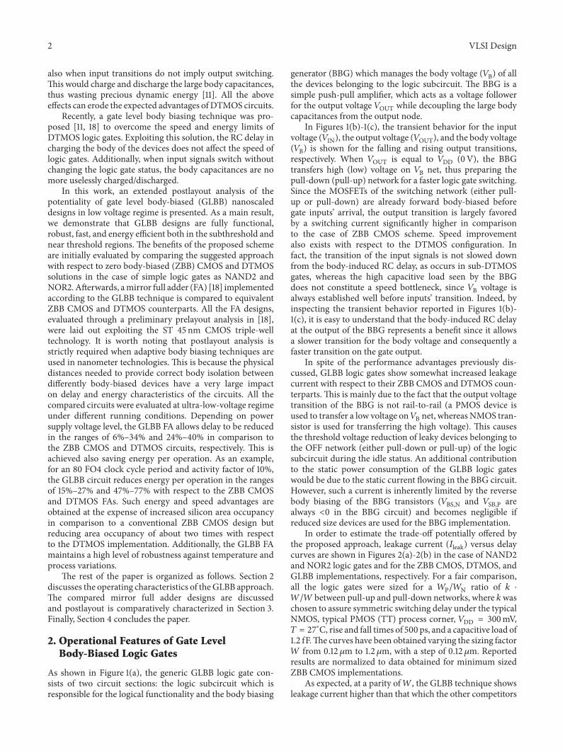
As shown in Figure 1(a), the generic GLBB logic gate con-sists of two circuit sections: the logic subcircuit which isresponsible for the logical functionality and the body biasing
generator (BBG) which manages the body voltage (𝑉B) of allthe devices belonging to the logic subcircuit. The BBG is asimple push-pull amplifier, which acts as a voltage followerfor the output voltage 𝑉OUT while decoupling the large bodycapacitances from the output node.
In Figures 1(b)-1(c), the transient behavior for the inputvoltage (𝑉IN), the output voltage (𝑉OUT), and the body voltage(𝑉B) is shown for the falling and rising output transitions,respectively. When 𝑉OUT is equal to 𝑉DD (0V), the BBGtransfers high (low) voltage on 𝑉B net, thus preparing thepull-down (pull-up) network for a faster logic gate switching.Since the MOSFETs of the switching network (either pull-up or pull-down) are already forward body-biased beforegate inputs’ arrival, the output transition is largely favoredby a switching current significantly higher in comparisonto the case of ZBB CMOS scheme. Speed improvementalso exists with respect to the DTMOS configuration. Infact, the transition of the input signals is not slowed downfrom the body-induced RC delay, as occurs in sub-DTMOSgates, whereas the high capacitive load seen by the BBGdoes not constitute a speed bottleneck, since 𝑉B voltage isalways established well before inputs’ transition. Indeed, byinspecting the transient behavior reported in Figures 1(b)-1(c), it is easy to understand that the body-induced RC delayat the output of the BBG represents a benefit since it allowsa slower transition for the body voltage and consequently afaster transition on the gate output.
In spite of the performance advantages previously dis-cussed, GLBB logic gates show somewhat increased leakagecurrent with respect to their ZBB CMOS and DTMOS coun-terparts. This is mainly due to the fact that the output voltagetransition of the BBG is not rail-to-rail (a PMOS device isused to transfer a low voltage on𝑉B net, whereas NMOS tran-sistor is used for transferring the high voltage). This causesthe threshold voltage reduction of leaky devices belonging tothe OFF network (either pull-down or pull-up) of the logicsubcircuit during the idle status. An additional contributionto the static power consumption of the GLBB logic gateswould be due to the static current flowing in the BBG circuit.However, such a current is inherently limited by the reversebody biasing of the BBG transistors (𝑉BS,N and 𝑉SB,P arealways <0 in the BBG circuit) and becomes negligible ifreduced size devices are used for the BBG implementation.
In order to estimate the trade-off potentially offered bythe proposed approach, leakage current (𝐼leak) versus delaycurves are shown in Figures 2(a)-2(b) in the case of NAND2and NOR2 logic gates and for the ZBB CMOS, DTMOS, andGLBB implementations, respectively. For a fair comparison,all the logic gates were sized for a 𝑊P/𝑊N ratio of 𝑘 ⋅𝑊/𝑊 between pull-up and pull-down networks, where 𝑘waschosen to assure symmetric switching delay under the typicalNMOS, typical PMOS (TT) process corner, 𝑉DD = 300mV,𝑇 = 27
∘C, rise and fall times of 500 ps, and a capacitive load of1.2 fF.The curves have been obtained varying the sizing factor𝑊 from 0.12 𝜇m to 1.2 𝜇m, with a step of 0.12 𝜇m. Reportedresults are normalized to data obtained for minimum sizedZBB CMOS implementations.
As expected, at a parity of𝑊, the GLBB technique showsleakage current higher than that which the other competitors
VLSI Design 3
Logic subcircuit
To the bulk of thelogic subcircuit devices
BBG circuit
Pull-upnetwork
Pull-downnetwork
VBVIN VOUT
(a)
Volta
ge
Time
VIN
VOUT
VB
(b)
Volta
ge
Time
VB
VIN VOUT
(c)
Figure 1: Logic gate with gate level dynamic body biasing (a) and transient behavior for output falling (b) and rising (c) voltage.
I lea
k(a
.u.)
Delay (a.u.)
18
12
6
0
0.4 0.6 0.8 1.0
W
1.2 𝜇m
0.12 𝜇m
CMOSDTMOSGLBB
(a)
I lea
k(a
.u.)
Delay (a.u.)
18
12
6
0
0.4 0.6 0.8 1.0
W
1.2 𝜇m
0.12 𝜇m
CMOSDTMOSGLBB
(b)
Figure 2: Leakage current delay plots for NAND2 (a) and NOR2 (b) logic gates.
show.Thismeans that, among the different evaluated choices,the GLBB style is the less suitable if theminimization of staticpower is the main design target. On the contrary, if the speedrequirement represents the main design aim, the GLBB stylebecomes the most reasonable choice allowing higher perfor-mance to be reached at the parity of leakage power consump-tion since the boosting action of the BBG allows the delaytarget to be reached using smaller transistors. Moreover, the
GLBB technique allows performance ranges which are unaf-fordable for both ZBB CMOS and DTMOS configurations.
3. Benchmark Circuit and PostlayoutComparative Analysis
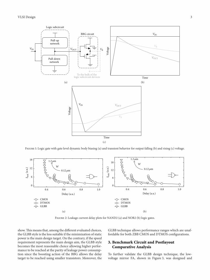
To further validate the GLBB design technique, the low-voltage mirror FA, shown in Figure 3, was designed and
4 VLSI Design
A
A
A
A
B
BB
B
Ci
Ci
A B
A
Ci
CiB A
B
Ci
Ci
CoS
B
A
Carry block Sum block
BBG
VB_1
VB_1
VB_1 VB_1
VB_1VB_1
VDD
VDDVDD
VB_1
VB_1 VB_1
VB_1
VB_1VB_2
VB_2
VB_2
VB_3 VB_3 VB_3 VB_3
VB_3VB_3
VB_3
VB_3
VB_3
VB_3VB_3VB_3
VB_3
VB_3
VB_3VB_4
VB_4
VB_4
Figure 3: Low-voltage mirror FA designed according to the GLBB technique.
Table 1: Pull-up/pull-down width ratio.
Stack config. ZBB DTMOS GLBB1 1.5𝑊/𝑊 𝑊/𝑊 1.1𝑊/𝑊2 4.5𝑊/2.5𝑊 2.5𝑊/2.5𝑊 3.2𝑊/2.5𝑊3 8.25𝑊/4.5𝑊 4.5𝑊/4𝑊 5.5𝑊/4.5𝑊
postlayoutwas characterized in comparison to correspondentZBB CMOS and DTMOS designs. Four BBGs are used tospeed up the switching of logic subcircuits. This translatesin eight additional devices in comparison to CMOS andDTMOS circuits.
Devices belonging to the logic subsections of comparedcircuits were sizedwithminimumchannel length (i.e.,𝐿min =40 nm), whereas the pull-up/pull-down channel width ratiowas chosen to obtain comparable strength for 𝑉DD = 0.3Vand 𝑇 = 27∘C, imposing equal width for series-connectedtransistors.
In Table 1, the width ratio between pull-up and pull-downnetworks is explicitly reported for the compared designs andfor the different stacking configurations. The sizing factor𝑊was chosen by iterative simulations, imposing similar leakagecurrent at nominal conditions (i.e., TT process corner,𝑉DD =0.3V, and 𝑇 = 27∘C) for all the compared designs.
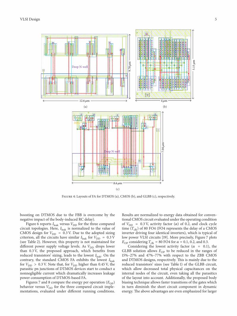
In order to correctly take into account the impact oflayout parasitics on performance, the physical design of thecompared circuits was carried out (see Figure 4) consideringthe design rules imposed by the ST 45 nm bulk CMOS triple-well technology. For DTMOS and GLBB designs, the deepN-well layer was used to shield N-channel devices fromthe P-type general substrate, thus obtaining P-well regionsisolated from the underlying substrate. Each of these regionsis vertically surrounded by an N-well region to providealso lateral isolation [14, 15]. Due to distances needed toprovide correct body isolation between differently body-biased devices, implementations exploiting unconventionalbody biasing (i.e., DTMOS and GLBB) exhibit significantly
Table 2: Comparison between ZBB, DTMOS, andGLBB schemes atnominal conditions (TT process corner,𝑉DD = 0.3V, and 𝑇 = 27∘C).
ZBB DTMOS GLBB
Silicon area [𝜇m2] 20.7 123.2 60.5
Delay [𝜇s] 0.70 0.78 0.59
Leakage current [nA] 0.20 0.24 0.21Energy per operation(𝑇 = 80 FO4, 𝛼 = 0.2) [fJ]
0.75 2.27 0.57
increased silicon area occupancy in comparison to the ZBBCMOS circuit. In an area optimized layout, the DTMOSimplementation requires one isolated P-well region for eachdifferent transistor gate signal, thus requiring 5 differentisolated P-well islands. On the contrary, in the proposedapproach, the number of isolated P-type islands is reducedto 4 (i.e., one for each BBG). This, along with the reducedsize of its transistors, leads the proposed implementation toreduce silicon area occupancy of more than 50% with respectto theDTMOSdesign. Table 2 reports postlayout comparisonresults under nominal simulation conditions.
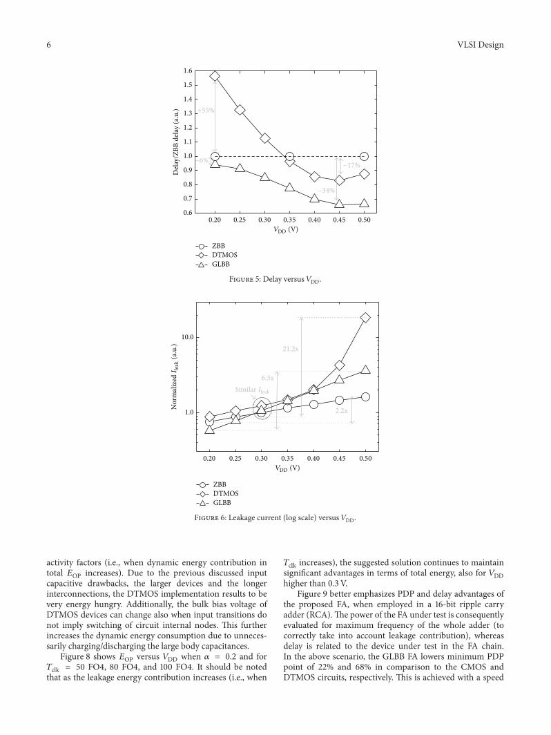
Comparative postlayout delay results, evaluated for 𝑉DDranging from 0.2V to 0.5 V with a voltage step of 0.05V,are shown in Figure 5. Given results are normalized withrespect to the delay of ZBB CMOS design. For 𝑉DD = 0.5V,the suggested approach allows delay to be reduced to 34%and 24% with respect to the standard CMOS and DTMOSimplementations, respectively. Observing the insert ofFigure 5, it is easy to note that as 𝑉DD decreases below 0.45V,the impact of FBB in boosting the performance is reduced butwith a different rate on GLBB and DTMOS techniques. Asfinal effect of this, the speed benefit brought by the suggestedapproach over the conventional CMOS circuit reduces downto 6% for the minimum considered power supply voltage(i.e., 𝑉DD = 0.2V). On the contrary, the speed advantageswith respect to the DTMOS implementation become morepronounced coming up to 60% for 𝑉DD = 0.2V (the speed
VLSI Design 5
12.6 𝜇m
9.78𝜇
m
Deep N-well
(a)
4𝜇m
5.15𝜇
m
(b)
8.6 𝜇m
7.04𝜇
m
Deep N-well
BBG
(c)
Figure 4: Layouts of FA for DTMOS (a), CMOS (b), and GLBB (c), respectively.
boosting on DTMOS due to the FBB is overcome by thenegative impact of the body-induced RC delay).
Figure 6 reports 𝐼leak versus 𝑉DD for the three comparedcircuit topologies. Here, 𝐼leak is normalized to the value ofCMOS design for 𝑉DD = 0.3V. Due to the adopted sizingcriterion, all the circuits have similar 𝐼leak for 𝑉DD = 0.3V(see Table 2). However, this property is not maintained fordifferent power supply voltage levels. As 𝑉DD drops lowerthan 0.3 V, the proposed approach, which benefits fromreduced transistors’ sizing, leads to the lowest 𝐼leak. On thecontrary, the standard CMOS FA exhibits the lowest 𝐼leakfor 𝑉DD > 0.3V. Note that, for 𝑉DD higher than 0.45V, theparasitic pn junctions of DTMOS devices start to conduct anonnegligible current which dramatically increases leakagepower consumption of DTMOS-based FA.
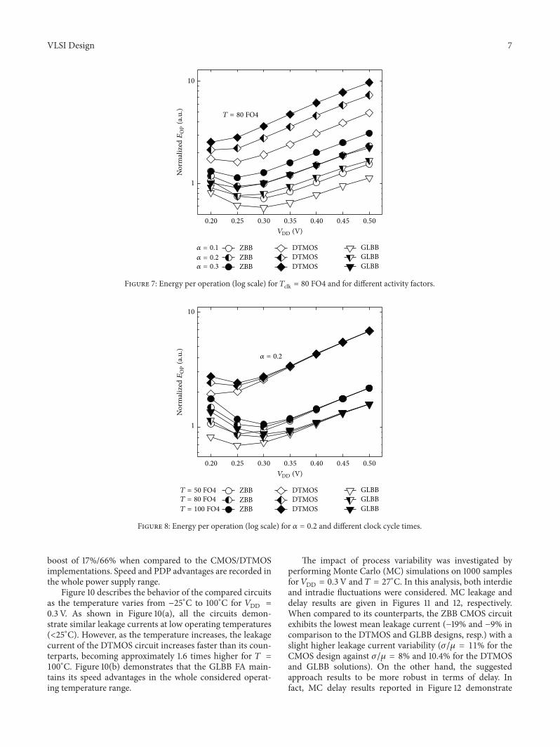
Figures 7 and 8 compare the energy per operation (𝐸OP)behavior versus 𝑉DD for the three compared circuit imple-mentations, evaluated under different running conditions.
Results are normalized to energy data obtained for conven-tional CMOS circuit evaluated under the operating conditionof 𝑉DD = 0.3V, activity factor (𝛼) of 0.2, and clock cycletime (𝑇clk) of 80 FO4 (FO4 represents the delay of a CMOSinverter driving four identical inverters), which is typical oflow power VLSI circuits [19]. More precisely, Figure 7 plots𝐸OP considering 𝑇clk = 80 FO4 for 𝛼 = 0.1, 0.2, and 0.3.
Considering the lowest activity factor (𝛼 = 0.1), theGLBB solution allows 𝐸OP to be reduced in the ranges of15%–27% and 47%–77% with respect to the ZBB CMOSand DTMOS designs, respectively. This is mainly due to thereduced transistors’ sizes (see Table 1) of the GLBB circuit,which allow decreased total physical capacitances on theinternal nodes of the circuit, even taking all the parasiticsof the layout into account. Additionally, the proposed bodybiasing technique allows faster transitions of the gates whichin turn diminish the short circuit component in dynamicenergy. The above advantages are even emphasized for larger
6 VLSI Design
VDD (V)
Dela
y/ZB
B de
lay (a
.u.)
1.6
1.5
1.4
1.3
1.2
1.1
1.0
0.9
0.8
0.7
0.60.20 0.25 0.30 0.35 0.40 0.45 0.50
−17%
−34%
−6%
+55%
ZBBDTMOSGLBB
Figure 5: Delay versus 𝑉DD.
VDD (V)0.20 0.25 0.30 0.35 0.40 0.45 0.50
ZBBDTMOSGLBB
Similar Ileak
6.3x
2.2xNor
mal
ized
I lea
k(a
.u.)
10.0
1.0
21.2x
Figure 6: Leakage current (log scale) versus 𝑉DD.
activity factors (i.e., when dynamic energy contribution intotal 𝐸OP increases). Due to the previous discussed inputcapacitive drawbacks, the larger devices and the longerinterconnections, the DTMOS implementation results to bevery energy hungry. Additionally, the bulk bias voltage ofDTMOS devices can change also when input transitions donot imply switching of circuit internal nodes. This furtherincreases the dynamic energy consumption due to unneces-sarily charging/discharging the large body capacitances.
Figure 8 shows 𝐸OP versus 𝑉DD when 𝛼 = 0.2 and for𝑇clk = 50 FO4, 80 FO4, and 100 FO4. It should be notedthat as the leakage energy contribution increases (i.e., when
𝑇clk increases), the suggested solution continues to maintainsignificant advantages in terms of total energy, also for 𝑉DDhigher than 0.3 V.
Figure 9 better emphasizes PDP and delay advantages ofthe proposed FA, when employed in a 16-bit ripple carryadder (RCA).The power of the FA under test is consequentlyevaluated for maximum frequency of the whole adder (tocorrectly take into account leakage contribution), whereasdelay is related to the device under test in the FA chain.In the above scenario, the GLBB FA lowers minimum PDPpoint of 22% and 68% in comparison to the CMOS andDTMOS circuits, respectively. This is achieved with a speed
VLSI Design 7
VDD (V)0.20 0.25 0.30 0.35 0.40 0.45 0.50
ZBBZBBZBB
DTMOSDTMOSDTMOS
GLBBGLBBGLBB
𝛼 = 0.1
𝛼 = 0.2𝛼 = 0.3
Nor
mal
ized
EO
P(a
.u.)
10
1
T = 80 FO4
Figure 7: Energy per operation (log scale) for 𝑇clk = 80 FO4 and for different activity factors.
VDD (V)0.20 0.25 0.30 0.35 0.40 0.45 0.50
ZBBZBBZBB
DTMOSDTMOSDTMOS
GLBBGLBBGLBB
𝛼 = 0.2
Nor
mal
ized
EO
P(a
.u.)
10
1
T = 80 FO4T = 50 FO4
T = 100 FO4
Figure 8: Energy per operation (log scale) for 𝛼 = 0.2 and different clock cycle times.
boost of 17%/66% when compared to the CMOS/DTMOSimplementations. Speed and PDP advantages are recorded inthe whole power supply range.
Figure 10 describes the behavior of the compared circuitsas the temperature varies from −25∘C to 100∘C for 𝑉DD =0.3V. As shown in Figure 10(a), all the circuits demon-strate similar leakage currents at low operating temperatures(<25∘C). However, as the temperature increases, the leakagecurrent of the DTMOS circuit increases faster than its coun-terparts, becoming approximately 1.6 times higher for 𝑇 =100∘C. Figure 10(b) demonstrates that the GLBB FA main-
tains its speed advantages in the whole considered operat-ing temperature range.
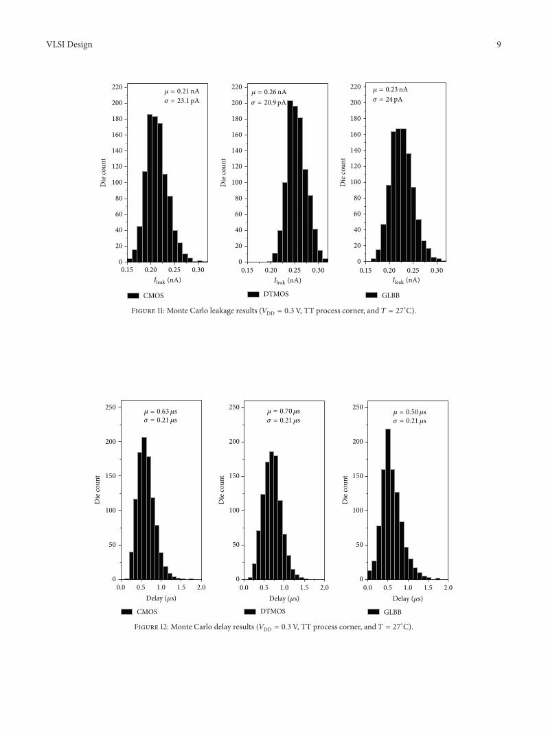
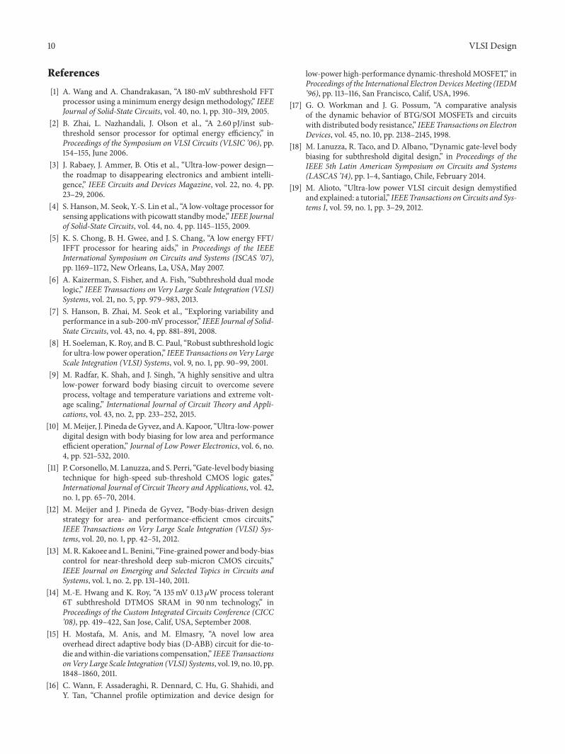
The impact of process variability was investigated byperforming Monte Carlo (MC) simulations on 1000 samplesfor 𝑉DD = 0.3V and 𝑇 = 27∘C. In this analysis, both interdieand intradie fluctuations were considered. MC leakage anddelay results are given in Figures 11 and 12, respectively.When compared to its counterparts, the ZBB CMOS circuitexhibits the lowest mean leakage current (−19% and −9% incomparison to the DTMOS and GLBB designs, resp.) with aslight higher leakage current variability (𝜎/𝜇 = 11% for theCMOS design against 𝜎/𝜇 = 8% and 10.4% for the DTMOSand GLBB solutions). On the other hand, the suggestedapproach results to be more robust in terms of delay. Infact, MC delay results reported in Figure 12 demonstrate
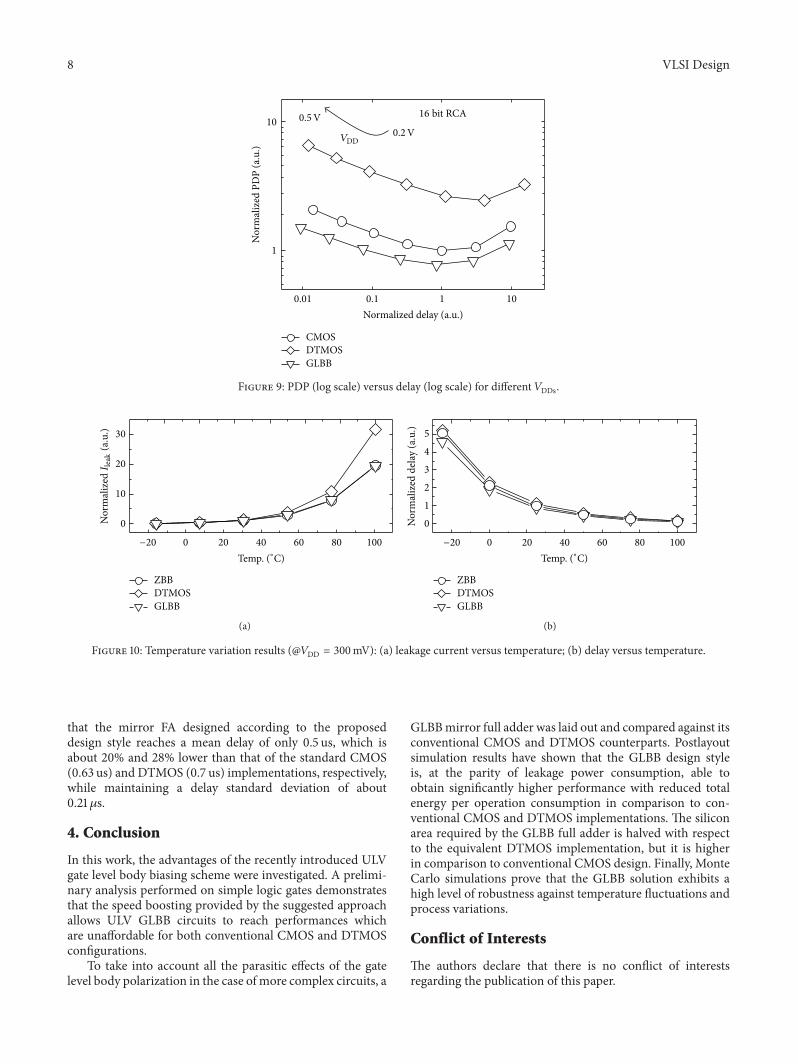
8 VLSI Design
CMOSDTMOSGLBB
Nor
mal
ized
PD
P (a
.u.)
Normalized delay (a.u.)
0.5V0.2V
VDD
16 bit RCA10
1
0.01 0.1 1 10
Figure 9: PDP (log scale) versus delay (log scale) for different 𝑉DDs.
30
20
10
0
−20 0 20 40 60 80 100
Nor
mal
ized
I lea
k(a
.u.)
ZBBDTMOSGLBB
Temp. (∘C)
(a)
Nor
mal
ized
del
ay (a
.u.) 5
4
3
2
1
0
−20 0 20 40 60 80 100
ZBBDTMOSGLBB
Temp. (∘C)
(b)
Figure 10: Temperature variation results (@𝑉DD = 300mV): (a) leakage current versus temperature; (b) delay versus temperature.
that the mirror FA designed according to the proposeddesign style reaches a mean delay of only 0.5 us, which isabout 20% and 28% lower than that of the standard CMOS(0.63 us) and DTMOS (0.7 us) implementations, respectively,while maintaining a delay standard deviation of about0.21𝜇s.
4. Conclusion
In this work, the advantages of the recently introduced ULVgate level body biasing scheme were investigated. A prelimi-nary analysis performed on simple logic gates demonstratesthat the speed boosting provided by the suggested approachallows ULV GLBB circuits to reach performances whichare unaffordable for both conventional CMOS and DTMOSconfigurations.
To take into account all the parasitic effects of the gatelevel body polarization in the case of more complex circuits, a
GLBBmirror full adder was laid out and compared against itsconventional CMOS and DTMOS counterparts. Postlayoutsimulation results have shown that the GLBB design styleis, at the parity of leakage power consumption, able toobtain significantly higher performance with reduced totalenergy per operation consumption in comparison to con-ventional CMOS and DTMOS implementations. The siliconarea required by the GLBB full adder is halved with respectto the equivalent DTMOS implementation, but it is higherin comparison to conventional CMOS design. Finally, MonteCarlo simulations prove that the GLBB solution exhibits ahigh level of robustness against temperature fluctuations andprocess variations.
Conflict of Interests
The authors declare that there is no conflict of interestsregarding the publication of this paper.
VLSI Design 9
Ileak (nA) Ileak (nA) Ileak (nA)
Die
coun
t
Die
coun
t
Die
coun
t
CMOS DTMOS GLBB
𝜇 = 0.21nA𝜎 = 23.1pA
𝜇 = 0.26nA𝜎 = 20.9 pA
𝜇 = 0.23nA𝜎 = 24pA
220
200
180
160
140
120
100
80
60
40
20
0
220
200
180
160
140
120
100
80
60
40
20
0
220
200
180
160
140
120
100
80
60
40
20
00.15 0.20 0.25 0.30 0.15 0.20 0.25 0.30 0.15 0.20 0.25 0.30
Figure 11: Monte Carlo leakage results (𝑉DD = 0.3V, TT process corner, and 𝑇 = 27∘C).
Die
coun
t
Die
coun
t
Die
coun
t
CMOS DTMOS GLBB
𝜇 = 0.63𝜇s𝜎 = 0.21 𝜇s
𝜇 = 0.70𝜇s𝜎 = 0.21 𝜇s
𝜇 = 0.50𝜇s𝜎 = 0.21 𝜇s
Delay (𝜇s)Delay (𝜇s)Delay (𝜇s)
250
200
150
100
50
0
250
200
150
100
50
0
250
200
150
100
50
00.0 0.5 1.0 1.5 2.00.0 0.5 1.0 1.5 2.00.0 0.5 1.0 1.5 2.0
Figure 12: Monte Carlo delay results (𝑉DD = 0.3V, TT process corner, and 𝑇 = 27∘C).
10 VLSI Design
References
[1] A. Wang and A. Chandrakasan, “A 180-mV subthreshold FFTprocessor using a minimum energy design methodology,” IEEEJournal of Solid-State Circuits, vol. 40, no. 1, pp. 310–319, 2005.
[2] B. Zhai, L. Nazhandali, J. Olson et al., “A 2.60 pJ/inst sub-threshold sensor processor for optimal energy efficiency,” inProceedings of the Symposium on VLSI Circuits (VLSIC ’06), pp.154–155, June 2006.
[3] J. Rabaey, J. Ammer, B. Otis et al., “Ultra-low-power design—the roadmap to disappearing electronics and ambient intelli-gence,” IEEE Circuits and Devices Magazine, vol. 22, no. 4, pp.23–29, 2006.
[4] S. Hanson, M. Seok, Y.-S. Lin et al., “A low-voltage processor forsensing applications with picowatt standbymode,” IEEE Journalof Solid-State Circuits, vol. 44, no. 4, pp. 1145–1155, 2009.
[5] K. S. Chong, B. H. Gwee, and J. S. Chang, “A low energy FFT/IFFT processor for hearing aids,” in Proceedings of the IEEEInternational Symposium on Circuits and Systems (ISCAS ’07),pp. 1169–1172, New Orleans, La, USA, May 2007.
[6] A. Kaizerman, S. Fisher, and A. Fish, “Subthreshold dual modelogic,” IEEE Transactions on Very Large Scale Integration (VLSI)Systems, vol. 21, no. 5, pp. 979–983, 2013.
[7] S. Hanson, B. Zhai, M. Seok et al., “Exploring variability andperformance in a sub-200-mVprocessor,” IEEE Journal of Solid-State Circuits, vol. 43, no. 4, pp. 881–891, 2008.
[8] H. Soeleman, K. Roy, and B. C. Paul, “Robust subthreshold logicfor ultra-low power operation,” IEEETransactions onVery LargeScale Integration (VLSI) Systems, vol. 9, no. 1, pp. 90–99, 2001.
[9] M. Radfar, K. Shah, and J. Singh, “A highly sensitive and ultralow-power forward body biasing circuit to overcome severeprocess, voltage and temperature variations and extreme volt-age scaling,” International Journal of Circuit Theory and Appli-cations, vol. 43, no. 2, pp. 233–252, 2015.
[10] M.Meijer, J. Pineda deGyvez, andA.Kapoor, “Ultra-low-powerdigital design with body biasing for low area and performanceefficient operation,” Journal of Low Power Electronics, vol. 6, no.4, pp. 521–532, 2010.
[11] P. Corsonello,M. Lanuzza, and S. Perri, “Gate-level body biasingtechnique for high-speed sub-threshold CMOS logic gates,”International Journal of CircuitTheory and Applications, vol. 42,no. 1, pp. 65–70, 2014.
[12] M. Meijer and J. Pineda de Gyvez, “Body-bias-driven designstrategy for area- and performance-efficient cmos circuits,”IEEE Transactions on Very Large Scale Integration (VLSI) Sys-tems, vol. 20, no. 1, pp. 42–51, 2012.
[13] M.R.Kakoee andL. Benini, “Fine-grained power and body-biascontrol for near-threshold deep sub-micron CMOS circuits,”IEEE Journal on Emerging and Selected Topics in Circuits andSystems, vol. 1, no. 2, pp. 131–140, 2011.
[14] M.-E. Hwang and K. Roy, “A 135mV 0.13𝜇W process tolerant6T subthreshold DTMOS SRAM in 90 nm technology,” inProceedings of the Custom Integrated Circuits Conference (CICC’08), pp. 419–422, San Jose, Calif, USA, September 2008.
[15] H. Mostafa, M. Anis, and M. Elmasry, “A novel low areaoverhead direct adaptive body bias (D-ABB) circuit for die-to-die andwithin-die variations compensation,” IEEE TransactionsonVery Large Scale Integration (VLSI) Systems, vol. 19, no. 10, pp.1848–1860, 2011.
[16] C. Wann, F. Assaderaghi, R. Dennard, C. Hu, G. Shahidi, andY. Tan, “Channel profile optimization and device design for
low-power high-performance dynamic-thresholdMOSFET,” inProceedings of the International Electron DevicesMeeting (IEDM’96), pp. 113–116, San Francisco, Calif, USA, 1996.
[17] G. O. Workman and J. G. Possum, “A comparative analysisof the dynamic behavior of BTG/SOI MOSFETs and circuitswith distributed body resistance,” IEEE Transactions on ElectronDevices, vol. 45, no. 10, pp. 2138–2145, 1998.
[18] M. Lanuzza, R. Taco, and D. Albano, “Dynamic gate-level bodybiasing for subthreshold digital design,” in Proceedings of theIEEE 5th Latin American Symposium on Circuits and Systems(LASCAS ’14), pp. 1–4, Santiago, Chile, February 2014.
[19] M. Alioto, “Ultra-low power VLSI circuit design demystifiedand explained: a tutorial,” IEEETransactions onCircuits and Sys-tems I, vol. 59, no. 1, pp. 3–29, 2012.

International Journal of
AerospaceEngineeringHindawi Publishing Corporationhttp://www.hindawi.com Volume 2014
RoboticsJournal of
Hindawi Publishing Corporationhttp://www.hindawi.com Volume 2014
Hindawi Publishing Corporationhttp://www.hindawi.com Volume 2014
Active and Passive Electronic Components
Control Scienceand Engineering
Journal of
Hindawi Publishing Corporationhttp://www.hindawi.com Volume 2014
International Journal of
RotatingMachinery
Hindawi Publishing Corporationhttp://www.hindawi.com Volume 2014
Hindawi Publishing Corporation http://www.hindawi.com
Journal ofEngineeringVolume 2014
Submit your manuscripts athttp://www.hindawi.com
VLSI Design
Hindawi Publishing Corporationhttp://www.hindawi.com Volume 2014
Hindawi Publishing Corporationhttp://www.hindawi.com Volume 2014
Shock and Vibration
Hindawi Publishing Corporationhttp://www.hindawi.com Volume 2014
Civil EngineeringAdvances in
Acoustics and VibrationAdvances in
Hindawi Publishing Corporationhttp://www.hindawi.com Volume 2014
Hindawi Publishing Corporationhttp://www.hindawi.com Volume 2014
Electrical and Computer Engineering
Journal of
Advances inOptoElectronics
Hindawi Publishing Corporation http://www.hindawi.com
Volume 2014
The Scientific World JournalHindawi Publishing Corporation http://www.hindawi.com Volume 2014
SensorsJournal of
Hindawi Publishing Corporationhttp://www.hindawi.com Volume 2014
Modelling & Simulation in EngineeringHindawi Publishing Corporation http://www.hindawi.com Volume 2014
Hindawi Publishing Corporationhttp://www.hindawi.com Volume 2014
Chemical EngineeringInternational Journal of Antennas and
Propagation
International Journal of
Hindawi Publishing Corporationhttp://www.hindawi.com Volume 2014
Hindawi Publishing Corporationhttp://www.hindawi.com Volume 2014
Navigation and Observation
International Journal of
Hindawi Publishing Corporationhttp://www.hindawi.com Volume 2014
DistributedSensor Networks
International Journal of