Embed Size (px)
Citation preview
Research ArticleGrowth and Device Performance of AlGaN/GaN Heterostructurewith AlSiC Precoverage on Silicon Substrate
Jae-Hoon Lee1 and Jung-Hee Lee2
1 Discrete Development Team, System LSI, Samsung Electronics Co., Ltd., Giheung 446-711, Republic of Korea2The School of Electronic Engineering & Computer Science, Kyungpook National University, Daegu 702-701, Republic of Korea
Correspondence should be addressed to Jae-Hoon Lee; [email protected]
Received 2 May 2014; Revised 31 July 2014; Accepted 11 August 2014; Published 11 September 2014
Academic Editor: Simone Mazzucato
Copyright © 2014 J.-H. Lee and J.-H. Lee. This is an open access article distributed under the Creative Commons AttributionLicense, which permits unrestricted use, distribution, and reproduction in any medium, provided the original work is properlycited.
A crack-free AlGaN/GaN heterostructure was grown on 4-inch Si (111) substrate with initial dot-like AlSiC precoverage layer. It isbelieved that introducing the AlSiC layer between AlN wetting layer and Si substrate is more effective in obtaining a compressivelystressed film growth than conventional Al precoverage on Si surface. The metal semiconductor field effect transistor (MESFET),fabricated on the AlGaN/GaN heterostructure grown with the AlSiC layer, exhibited normally on characteristics, such as thresholdvoltage of −2.3 V, maximum drain current of 370mA/mm, and transconductance of 124mS/mm.
1. Introduction
Group III-nitride semiconductors and their ternary solidsolutions are very promising materials for both short wave-length optoelectronics and power electronic devices [1–4]. The AlGaN/GaN heterostructure field effect transistors(HFETs) have a great potential for future high-frequencyand high-power applications because of the intrinsic advan-tages of materials such as wide band gap, high breakdownvoltage, and high electron peak velocity [5, 6]. Si substrateis considered as a promising candidate, which may replaceexpensive and small-sized wafers such as sapphire and SiC,even though the GaN layer grown on Si substrate has a largestrain and dislocation due to a large lattice mismatch andthermal expansion coefficient difference between the grownGaN layer and the Si substrate [7, 8]. The mismatch betweenthermal expansion coefficients is about 56%, which induces alarge tensile stress and may cause a severe crack generationin the grown GaN films during the cooling process aftergrowth.
A GaN film grown directly on Si using conventional two-step method usually exhibits poor surface morphology andlow crystal quality. In general, the GaN film grown on Si is
very sensitive to growth conditions such as MOCVD cham-ber condition, substrate, III/V ratio, temperature, pressure,source, and layer materials. Therefore, various types ofintermediate layer between the GaN epilayer and the Sisubstrate, such as 3C-SiC, AlN, GaAs, AlAs, Si
3N4, and r-
Al2O3, have been studied to improve the crystalline quality
of the GaN layer grown on Si substrate [9–12]. Steckl et al.[12] reported that (111) Si-on-insulator (SOI) structures canbe converted to single crystalline SiC by carbonization of thethin (<100 nm) Si layer using rapid thermal chemical vapordeposition with mixtures of propane and H
2at atmospheric
pressure. The structure of GaN films grown on (111) SiC SOIstructure is comparable toGaNgrownon sapphire substrates.This is because the single crystalline SiC interlayer decreaseslattice mismatch between the grown GaN layer and thesubstrate. However, this method requires additional ex situprocesseswhich cannot be always easily controlled. SinceAlNhas good wetting properties on Si substrate compared withother intermediate layers, the recent experimental resultshave concluded that an AlN buffer layer can alleviate thedifficulties in growing the GaN layer on Si substrate. Inaddition, the Al precoverage on the surface of Si substrate isperformed prior to the growth of the AlN layer to prevent
Hindawi Publishing CorporationAdvances in Materials Science and EngineeringVolume 2014, Article ID 290646, 6 pageshttp://dx.doi.org/10.1155/2014/290646

2 Advances in Materials Science and Engineering
HT-AIN
AlGaN grade layer
Undoped-GaN
GateSource Drain
PadPadPad
2DEG
AlSiC
Si substrate
∼2𝜇m
AlxGa1−x (∼20nm)
GaN: ∼0.1 𝜇m
AlGaN grade: ∼1.7 𝜇m
AIN: ∼0.2 𝜇mAlSiC
Si3N4
0.2 𝜇m
N
Si substrate
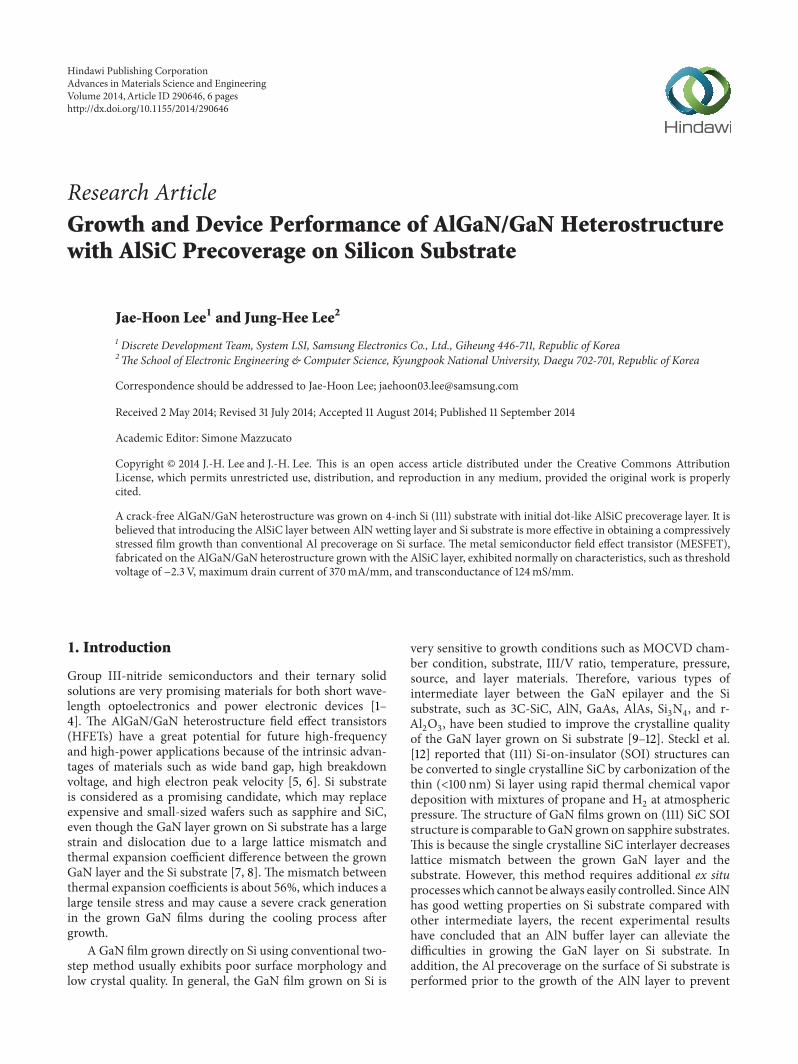
Figure 1: A schematic cross-sectional view and TEM image of the fabricated MESFET layer structure.
the formation of the amorphous SiN𝑥layer and hence to
obtain high crystal quality [13, 14], because the formation ofamorphous SiN
𝑥in the initial stage of the growth passivates
the surface and suppresses the GaN growth.In this work, for the purpose of reducing the crack density
in the AlGaN/GaN heterostructure grown on Si substrate, wehave covered dot-like AlSiC layer on the surface of the Sisubstrate prior to the growth of the AlN wetting layer. Thedevice performances of the normally on AlGaN/GaN HFETsfabricated on the Si substrate grown with AlSiC precoveragewere also demonstrated.
2. Experiments
The AlGaN/GaN heterostructure investigated in this workwas grown on 4-inch (111) p-type Si substrates by metalorganic chemical vapor deposition (MOCVD). Trimethyl-gallium (TMGa), trimethylaluminum (TMAl), carbon tetra-bromide (CBr
4), ditertiarybutylsilane (DTBSi), and ammonia
(NH3) were used for the precursors of Ga, Al, C, Si, and N,
respectively [15]. Prior to the growth of AlN wetting layer, theSi substrate was baked in an H
2ambient at 1100∘C for 10min
to remove the native oxide and then presurface coverage onthe Si substrate with AlSiC was performed for 60 secondsin order to prevent formation of amorphous SiN
𝑥layer.
For comparison, the heterostructure with conventional Alpresurface coverage was also grown. The layer structure withtotal thickness of about 2𝜇m consists of 200 nm thick hightemperature- (HT-) AlN layer, 1.7𝜇m thick AlGaN gradedlayer, 100 nm thickGaN layer, and 20 nm thickAlGaNbarrierin growth sequence [16].The Al content in the AlGaN barrieris 20%, determined by high-resolution X-ray diffraction(XRD). The mobility and the density of the two-dimensionalelectron gas (2DEG) formed at the AlGaN/GaN heterointer-face were 1100 cm2/V⋅s and 8 × 10¹²/cm2, respectively. For thedevice fabrication, the active region of the device was definedby inductively coupled plasma (ICP) reactive ion etchingusing a BCl
3/Cl2gas mixture. After opening contact holes,
Ti/Al/Ni/Au metal layer for Ohmic contact was deposited
and followed by rapid thermal annealing at 850∘C for 30 s inN2ambient.The specific contact resistance of 2× 10⁻⁵Ω⋅cm−2
was obtained for the annealed sample using transmission linemeasurements (TLM). After depositing Ni/Au for the gatemetal, Si
3N4interdielectric layer with thickness of 800 nm
was deposited to cover the entire surface of the device. Ti/Alpad metals were finally deposited to connect the gate andthe source/drain region. The current-voltage (I-V) charac-teristics were measured by using Agilent 4155 parameteranalyzer and STI curve tracer 5000E. A schematic cross-section and the transmission electron microscope (TEM)image of the fabricated metal semiconductor field effecttransistor (MESFET) are shown in Figure 1.
3. Results and Discussion
The existence of AlSiC precoverage layer on Si surface wasconfirmed by the secondary ion mass spectroscope (SIMS)analysis as shown in Figure 2(a). For the purpose of findingthe atomic composition of the AlSiC layer, a reference AlSiClayerwith thickness of 20 nmwas grownon Si substrate underthe same growth condition as the AlSiC precoverage layerin real epitaxial structure. X-Ray photoelectron spectroscopy(XPS) analysis for this AlSiC layer reveals that Al, Si, C, andO atoms exist in the AlSiC layer with atomic compositionof 37, 31, 23, and 9%, respectively, as shown in Figure 2(b).High concentrations of carbon and Si atoms were observedat interface between AlN buffer layer and Si substrate. Theslight C, Ga, and Al peaks also appear to be within thesilicon bulk, which is due to diffusion at high temperaturegrowth condition. Figures 2(c) and 2(d) show atomic forcemicroscopy (AFM) images for the surface of the Si substrateafter deposition of Al andAlSiC precoverage layer with corre-sponding rms roughness of 0.5 and 3.9 nm, respectively. It isnoticed that the grain size of the randomly distributed AlSiCprecoverage layer is larger than that of the Al precoverage.
The growth with AlSiC precoverage resulted in crack-freesurface while the layer with Al precoverage showed manycracks on the surface, as shown in Figure 3. This probably

Advances in Materials Science and Engineering 3
0.0 0.2 0.4 0.6 0.8 1.0 1.2 1.4 1.6 1.8 2.0
Si
C
AlGa
Al,
Ga c
once
ntra
tion
(ato
m fr
)
C, S
i con
cent
ratio
n (a
tom
s/cc
)10
1
0.1
0.01
1E − 3
1E − 4
1E − 5
1E − 6
1E22
1E21
1E20
1E19
1E18
1E17
1E16
Depth (𝜇m)
(a)
0 100 200 300 400 500 6000
10000
20000
30000
40000
O1s
C1sSi2p
Al2p
Inte
nsity
(a.u
.)
Binding energy (eV)
(b)
0.51.0
1.5(𝜇m)
(c)
0.51.0
1.5(𝜇m)
(d)
Figure 2: (a) SIMS profile of film grown on Si substrate with AlSiC precoverage layer in real epitaxial layer. (b) XPS measurement of 20 nmthick reference AlSiC film. (c) AFM images of Si surface covered with Al precoverage layer. (d) AFM images of Si surface covered with AlSiCprecoverage layer.
1mm
(a)
1mm
(b)
Figure 3: Optical photography of AlGaN/GaN surface grown on Si substrate with Al (a) and AlSiC precoverage interlayer (b).
explains that AlSiC precoverage is effective in compensatingthe tensile stress in the GaN layer grown on Si substrate. TheRaman scattering spectra shown in Figure 4(a) exhibit peakshift at frequencies of 567.08 and 568.53 cm−1 for the grownfilmwithAl andAlSiC precoverage, corresponding to the cal-culated biaxial stresses of 0.099 and −0.240GPa, respectively[17]. This indicates that the biaxial stress in the AlGaN/GaNheterostructure grownon Si substratewithAlSiCprecoverageis compressive while that with Al precoverage still remains
tensile, considering the reference value of 567.5 cm−1 forthe freestanding GaN. It is believed that the insertion ofAlSiC precoverage layer gives rise to strong compressivestress in the GaN film grown on Si substrate during the hightemperature growth, which sufficiently overcomes the tensilestress caused by cooling down and remains compressive evenafter completing the growth. Photoluminescence mappingin inset of Figure 4(a) showed the average peek wavelengthat 361.5 nm, which belongs to the shifted wavelength for

4 Advances in Materials Science and Engineering
500 510 520 530 540 550 560 570 580 590 600
Si
568.53567.08
Inte
nsity
(a.u
.)
Al precoverage AlSiC precoverage
105
104
103
102
Raman shift (cm−1)
E2-high peak of GaN
362.9
362.5
362.2
361.8
361.4
361.1
360.7
360.3
360.0
(nm
)
Avge.: 361.5Median.: 361.5Std. dev.: 0.060%
(0.217)In Space: 0.0% Below: 100.0% Above: 0.0%
Peak lambda
(a)
0 100 200 300 400 500Voltage (V)
Al precoverageAlSiC precoverage
Vert
ical
leak
age c
urre
nt (m
A/c
m2)
103
101
10−1
10−3
10−5
10−7
(b)
Figure 4: (a) Raman scattering spectra of AlGaN/GaN layers grown on Si substrate with Al and AlSiC precoverage layer. The inset showsthe map image of wavelength for grown films with AlSiC precoverage layer. (b) Vertical leakage current of AlGaN/GaN layers grown on Sisubstrate with Al and AlSiC precoverage layer.
0 2 4 6 8 100
50
100
150
200
250
300
350
400
Dra
in cu
rren
t (m
A/m
m)
Drain voltage (V)
VGs = −6∼1VStep = 1V
(a)
2
050
100150200250300350400
Gate voltage (V)
Dra
in cu
rren
t (m
A/m
m)
0
20
40
60
80
100
120
140
Tran
scon
duct
ance
(mS/
mm
) −50 −20
−10 −8 −6 −4 −2 0
VDS = 8V
(b)
Gat
e cur
rent
(A/m
m)
2Gate voltage (V)
−10 −8 −6 −4 −2 0
10−2
10−3
10−4
10−5
10−6
10−7
10−8
10−9
(c)
0 100 200 300 400 500 600
Dra
in cu
rren
t (A
/mm
)
Drain voltage (V)
VGs = −5V10−2
10−3
10−4
10−5
10−6
10−7
10−8
(d)
Figure 5: I-V characteristics of the fabricated device with AlSiC precoverage layer. (a) Drain current, (b) transfer characteristics, (c) gateleakage current, and (d) breakdown voltage.

Advances in Materials Science and Engineering 5
the compressively stressed GaN layer. On the other hand, thefilms with Al precoverage were not able to sufficiently over-come the tensile stress which resulted in generation of crackonGaN surface due to different thermal expansion coefficientafter cooling down. Figure 4(b) showed the vertical leakagecurrent-voltage (I-V) characteristics for both AlGaN/GaNheterostructure grown on Si substrate with Al and AlSiCprecoverage layer.The leakage current wasmeasured by usinga circular type pattern with diameter of 100 𝜇m betweenOhmic contact pads and Si substrate. As shown in Fig ure4(b), the film with Al precoverage layer exhibits the shortcharacteristics due to the crack path. On the other hand, thefilm with AlSiC precoverage layer exhibits relatively highersemi-insulating characteristics of 3 × 10⁸Ω (1 𝜇A at 300V),which make it attractive for high-power application.
Figure 5 shows the I-V characteristics for the normallyon AlGaN/GaN HFET fabricated on the grown AlGaN/GaNheterostructure with the AlSiC precoverage on the Sisubstrate. The gate length, the gate width, and the gate-to-drain distance of both devices were 2, 140, and 20 𝜇m,respectively. The total area of the device was 500 × 500𝜇m2.Themaximum drain current (𝐼dmax) and the specific on state-resistance (𝑅ON) of the normally on HFET are 370mA/mmand 5mΩ⋅cm2, respectively, as shown in Figure 5(a). Thethreshold voltage and the maximum transconductance (Gm)of device at a fixed𝑉DS of 8V are−2.3 V and 124mS/mm (𝐼DS-𝑉GS), respectively, as shown in Figure 5(b). The gate leakagecurrent is −5 𝜇A at gate voltage of −10V (Figure 5(c)), whichis comparable to that ofAlGaN/GaNHFETgrownon the sap-phire substrate [18]. In addition, the offstate breakdown volt-age of the device is as high as 550V (Figure 5(d)), even thoughno additional processes are applied to increase the breakdownvoltage, which demonstrates that the AlGaN/GaN HFETwith the AlSiC precoverage on the Si substrate has a greatpotential application to the high-power device.
4. Conclusion
To obtain a crack-free AlGaN/GaN heterostructure grownon Si substrate, we proposed the insertion of the AlSiCprecoverage layer between AlN and Si substrate. The AlSiCprecoverage layer generates the compressive stress in thefilm grown on Si substrate during the high temperaturegrowth, which resulted in crack-free films due to compen-sation of tensile stress after finishing epitaxial growth. Thefabricated normally on HFET exhibits a threshold voltage of−2.3 V, 𝐼dmax of 370mA/mm, 𝑅ON of 5mΩ⋅cm2, and Gm of124mS/mm.
Conflict of Interests
The authors declare that there is no conflict of interestsregarding the publication of this paper.
Acknowledgments
This work was partly supported by Kyungpook NationalUniversity Research Fund 2012, the BK21 Plus funded by
the Ministry of Education (21A20131600011), the IT R&DProgram of MOTIE/KEIT (10048931), and the NationalResearch Foundation of Korea (NRF) Grant funded by theKorean Government (MSIP) (nos. 2008-0062617 and 2011-0016222).
References
[1] S. Nakamura, M. Senoh, S.-I. Nagahama et al., “High-power,long-lifetime InGaN multi-quantum-well-structure laserdiodes,” Japanese Journal of Applied Physics, vol. 36, no. 8, pp.L1059–L1061, 1997.
[2] J.-H. Lee, D.-Y. Lee, B.-W. Oh, and J.-H. Lee, “Comparisonof InGaN-based LEDs grown on conventional sapphire andcone-shape-patterned sapphire substrate,” IEEETransactions onElectron Devices, vol. 57, no. 1, pp. 157–163, 2010.
[3] J. H. Lee, J. T. Oh, S. B. Choi, Y. C. Kim, and H. I. Cho,“Enhancement of InGaN-based vertical LED with concavelypatterned surface using patterned sapphire substrate,” IEEEPhotonics Technology Letters, vol. 20, no. 5, pp. 345–347, 2008.
[4] Y. Uemoto, M. Hikita, H. Ueno et al., “Gate injection tran-sistor (GIT)—a normally-off AlGaN/GaN power transistorusing conductivity modulation,” IEEE Transactions on ElectronDevices, vol. 54, no. 12, pp. 3393–3399, 2007.
[5] O. Ambacher, J. Smart, J. R. Shealy et al., “Two-dimensionalelectron gases induced by spontaneous and piezoelectric polar-ization charges in N- And Ga-face AIGaN/GaN heterostruc-tures,” Journal of Applied Physics, vol. 85, no. 6, pp. 3222–3233,1999.
[6] Y.-F. Wu, D. Kapolnek, J. P. Ibbetson, P. Parikh, B. P. Keller, andU. K. Mishra, “Very-high power density AlGaN/GaNHEMT’s,”IEEE Transactions on Electron Devices, vol. 48, no. 3, pp. 586–590, 2001.
[7] F. Semond, P. Lorenzini, N. Grandjean, and J. Massies,“High-electron-mobility AlGaN/GaN heterostructures grownon Si(111) by molecular-beam epitaxy,” Applied Physics Letters,vol. 78, no. 3, pp. 335–337, 2001.
[8] P. Kung, A. Saxler, X. Zhang et al., “High quality AIN andGaN epilayers grown on (001) sapphire, (100), and (111) siliconsubstrates,”Applied Physics Letters, vol. 66, pp. 2958–2960, 1995.
[9] Y. Nakada, I. Aksenov, and H. Okumura, “GaN heteroepitaxialgrowth on silicon nitride buffer layers formed on Si (111)surfaces by plasma-assisted molecular beam epitaxy,” AppliedPhysics Letters, vol. 73, no. 6, pp. 827–829, 1998.
[10] L. Wang, X. Liu, Y. Zan et al., “Wurtzite GaN epitaxial growthon a Si(001) substrate using 𝛾-Al
2O3as an intermediate layer,”
Applied Physics Letters, vol. 72, no. 1, pp. 109–111, 1998.[11] A. le Louarn, S. Vezian, F. Semond, and J. Massies, “AlN buffer
layer growth for GaN epitaxy on (111) Si: Al or N first?” Journalof Crystal Growth, vol. 311, no. 12, pp. 3278–3284, 2009.
[12] A. J. Steckl, J. Devrajan, C. Tran, and R. A. Stall, “SiC rapid ther-mal carbonization of the (111)Si semiconductor-on-insulatorstructure and subsequent metalorganic chemical vapor depo-sition of GaN,” Applied Physics Letters, vol. 69, no. 15, pp. 2264–2266, 1996.
[13] I.-H. Lee, S. J. Lim, and Y. Park, “Growth and optical propertiesof GaN on Si(1 1 1) substrates,” Journal of Crystal Growth, vol.235, no. 1–4, pp. 73–78, 2002.
[14] P. Chen, R. Zhang, Z. M. Zhao et al., “Growth of high qualityGaN layers with AlN buffer on Si(111) substrates,” Journal ofCrystal Growth, vol. 225, no. 2–4, pp. 150–154, 2001.

6 Advances in Materials Science and Engineering
[15] J.-H. Lee, J.-H. Jeong, and J.-H. Lee, “Enhanced electricalcharacteristics of AlGaN-based SBD with in situ depositedsilicon carbon nitride cap layer,” IEEE Electron Device Letters,vol. 33, no. 4, pp. 492–494, 2012.
[16] K. Cheng, M. Leys, S. Degroote et al., “Flat GaN epitaxial layersgrown on Si(111) by metalorganic vapor phase epitaxy usingstep-graded AlGaN intermediate layers,” Journal of ElectronicMaterials, vol. 35, no. 4, pp. 592–598, 2006.
[17] S. Tripathy, S. J. Chua, P. Chen, and Z. L. Miao, “Micro-Raman investigation of strain in GaN and Al
𝑥Ga1−𝑥
N/GaNheterostructures grown on Si(111),” Journal of Applied Physics,vol. 92, no. 7, pp. 3503–3510, 2002.
[18] J.-H. Lee, J.-H. Jeong, and J.-H. Lee, “Normally off GaN powerMOSFET grown on sapphire substrate with highly resistiveundoped buffer layer,” IEEE Electron Device Letters, vol. 33, no.10, pp. 1429–1431, 2012.

Submit your manuscripts athttp://www.hindawi.com
ScientificaHindawi Publishing Corporationhttp://www.hindawi.com Volume 2014
CorrosionInternational Journal of
Hindawi Publishing Corporationhttp://www.hindawi.com Volume 2014
Polymer ScienceInternational Journal of
Hindawi Publishing Corporationhttp://www.hindawi.com Volume 2014
Hindawi Publishing Corporationhttp://www.hindawi.com Volume 2014
CeramicsJournal of
Hindawi Publishing Corporationhttp://www.hindawi.com Volume 2014
CompositesJournal of
NanoparticlesJournal of
Hindawi Publishing Corporationhttp://www.hindawi.com Volume 2014
Hindawi Publishing Corporationhttp://www.hindawi.com Volume 2014
International Journal of
Biomaterials
Hindawi Publishing Corporationhttp://www.hindawi.com Volume 2014
NanoscienceJournal of
TextilesHindawi Publishing Corporation http://www.hindawi.com Volume 2014
Journal of
NanotechnologyHindawi Publishing Corporationhttp://www.hindawi.com Volume 2014
Journal of
CrystallographyJournal of
Hindawi Publishing Corporationhttp://www.hindawi.com Volume 2014
The Scientific World JournalHindawi Publishing Corporation http://www.hindawi.com Volume 2014
Hindawi Publishing Corporationhttp://www.hindawi.com Volume 2014
CoatingsJournal of
Advances in
Materials Science and EngineeringHindawi Publishing Corporationhttp://www.hindawi.com Volume 2014
Smart Materials Research
Hindawi Publishing Corporationhttp://www.hindawi.com Volume 2014
Hindawi Publishing Corporationhttp://www.hindawi.com Volume 2014
MetallurgyJournal of
Hindawi Publishing Corporationhttp://www.hindawi.com Volume 2014
BioMed Research International
MaterialsJournal of
Hindawi Publishing Corporationhttp://www.hindawi.com Volume 2014
Nano
materials
Hindawi Publishing Corporationhttp://www.hindawi.com Volume 2014
Journal ofNanomaterials