Embed Size (px)
Citation preview
Research ArticleDesign of Low Power and Efficient Carry Select AdderUsing 3-T XOR Gate
Gagandeep Singh and Chakshu Goel
ECE Department, Shaheed Bhagat Singh State Technical Campus, Ferozepur, Punjab 152004, India
Correspondence should be addressed to Chakshu Goel; [email protected]
Received 16 June 2014; Accepted 7 September 2014; Published 22 September 2014
Academic Editor: Liwen Sang
Copyright © 2014 G. Singh and C. Goel.This is an open access article distributed under theCreativeCommonsAttributionLicense,which permits unrestricted use, distribution, and reproduction in any medium, provided the original work is properly cited.
In digital systems, mostly adder lies in the critical path that affects the overall performance of the system. To perform fast additionoperation at low cost, carry select adder (CSLA) is the most suitable among conventional adder structures. In this paper, a 3-T XORgate is used to design an 8-bit CSLA as XOR gates are the essential blocks in designing higher bit adders. The proposed CSLA hasreduced transistor count and has lesser power consumption as well as power-delay product (PDP) as compared to regular CSLAand modified CSLA.
1. Introduction
In today’s VLSI circuit designs, there is a significant increasein the power consumption due to the increasing speedand complexity of the circuits. As the demand for portableequipment like laptops and cellular phones is increasingrapidly, great attention has been focused on power efficientcircuit designs [1–4]. Adders are the basic building blocksof the complex arithmetic circuits. Adders are widely usedin Central Processing Unit (CPU), Arithmetic Logic Unit(ALU), and floating point units, for address generation in caseof cache ormemory access and in digital signal processing [5–7].
Having adders with fast addition operation and lowpower along with low area consumption is still a challengingissue. Depending upon the area, delay, and power consump-tion, the various adders are categorized as ripple carry adder(RCA), carry select adder (CSLA), and carry lookahead adder(CLAA). CSLA provides a compromise between the largeareawith small delay of CLAAand small area but longer delayof RCA [8]. CSLA uses pair of RCAs for addition, that is, oneblock of RCA with 𝐶in (carry in) = 0 and other block of RCAwith 𝐶in = 1. Depending on the value of previous carry, thefinal sum and carry outputs are selected using multiplexer.Due to the pair of RCAs used for each bit addition, thesimplest kind of CSLA is not very efficient [9].
Keeping in mind that XOR gates are the building blocksof adders, here in this work, we use a 3T-XOR gate to designan 8-bit CSLA. The main advantage of using 3T-XOR gate isthat the power consumption of the circuit decreases due to thelarge decrease in number of switching transistors (MOSFETs)used in the design of 8-bit CSLA.
This paper is organized as follows. Section 2 presents theearlier works on carry select adder including the detailedstructure of regularCSLAaswell asmodifiedCSLA. Section 3explains the proposed CSLA and evaluates the reduction inswitching transistors (MOSFETs) count.The implementationdetails as well as simulation results of proposed CSLA areanalyzed in Section 4 and Section 5 concludes the wholework.
2. Earlier Works on Carry Select Adder
In digital adders, the speed of addition is limited due tothe time taken by the carry signal to propagate through theadder. The regular carry select adder (R-CSLA) was intro-duced to mitigate the problem of carry propagation delay byindependently generating multiple carries and then selectingthe correct sum and carry outputs depending on the valueof previous carry [9]. As previously discussed, this type ofCSLA (i.e., R-CSLA) was not area efficient due to the use ofpair of RCAs (each for 𝐶in = 0 and 𝐶in = 1) to produce
Hindawi Publishing CorporationAdvances in ElectronicsVolume 2014, Article ID 564613, 6 pageshttp://dx.doi.org/10.1155/2014/564613
2 Advances in Electronics
Full adder
A0 B0
1446 222
2
C0C2C4
23
11222233
000
11 1
Group 4 Group 3 Group 2 Group 1
Sum 0Sum [2: 1]Sum [4: 3]Sum [7: 5]
A [2:1] B [2:1]A [4:3] B [4:3]A [7:5] B [7:5]
4: 3 RCA
4: 3 RCA
2:1 RCA
2: 1 RCA
7: 5 RCA
7: 5 RCA
6: 3 Mux 6: 3 Mux8: 4 Mux
Cout
Cin
Figure 1: Regular 8-bit CSLA.
X0X1X2X3
B0B1
B0
B3 B2
X3 X2 X1 X0
B3 B2 B1 B0
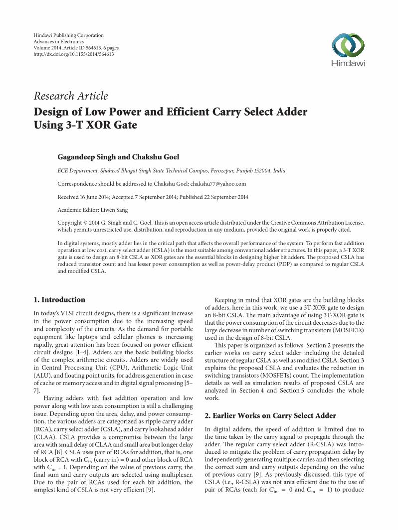
Figure 2: Four-bit BEC circuit.
the final sum and carry output. The 8-bit R-CSLA is shownin Figure 1.
To make low power consumption and an area efficientCSLA, an add-one circuit known as Binary to Excess-1Converter (BEC) circuit was introduced. This BEC circuitreplaced the RCA with 𝐶in = 1 used in R-CSLA as lessernumbers of logic gates were used in BEC as compared to 𝑛-bit RCA [10–12]. The truth table and circuit diagram of 4-bitBEC are shown in Figure 2 and Table 1, respectively.
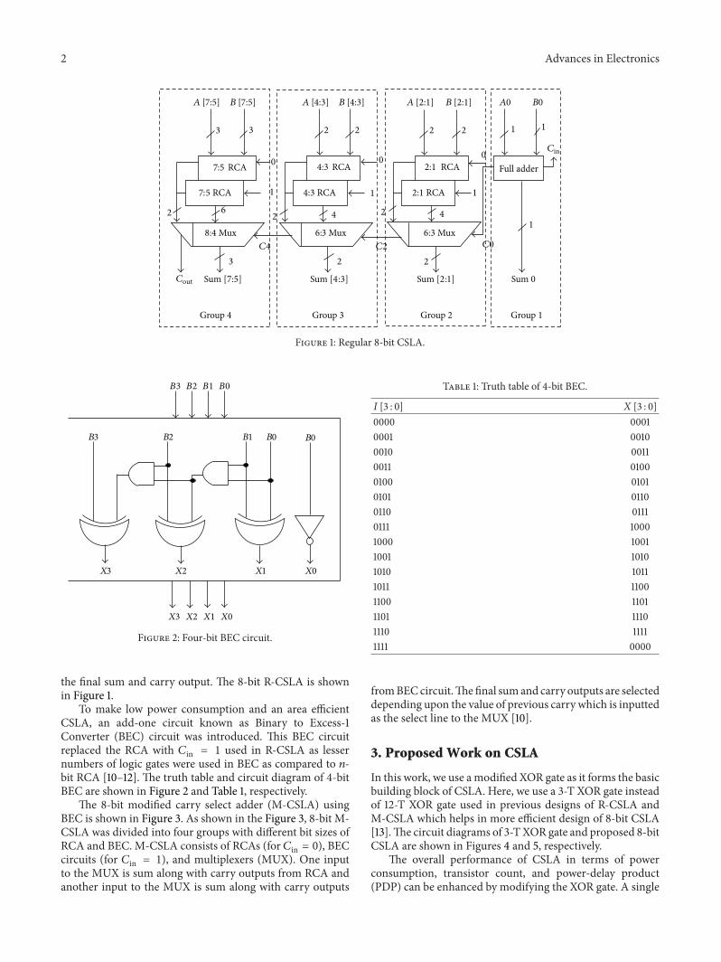
The 8-bit modified carry select adder (M-CSLA) usingBEC is shown in Figure 3. As shown in the Figure 3, 8-bit M-CSLA was divided into four groups with different bit sizes ofRCA and BEC. M-CSLA consists of RCAs (for 𝐶in = 0), BECcircuits (for 𝐶in = 1), and multiplexers (MUX). One inputto the MUX is sum along with carry outputs from RCA andanother input to the MUX is sum along with carry outputs
Table 1: Truth table of 4-bit BEC.
𝐼 [3 : 0] 𝑋 [3 : 0]0000 00010001 00100010 00110011 01000100 01010101 01100110 01110111 10001000 10011001 10101010 10111011 11001100 11011101 11101110 11111111 0000
fromBECcircuit.Thefinal sumand carry outputs are selecteddepending upon the value of previous carry which is inputtedas the select line to the MUX [10].
3. Proposed Work on CSLA
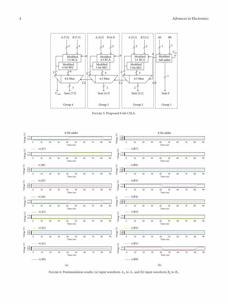
In this work, we use amodified XOR gate as it forms the basicbuilding block of CSLA. Here, we use a 3-T XOR gate insteadof 12-T XOR gate used in previous designs of R-CSLA andM-CSLA which helps in more efficient design of 8-bit CSLA[13].The circuit diagrams of 3-T XOR gate and proposed 8-bitCSLA are shown in Figures 4 and 5, respectively.
The overall performance of CSLA in terms of powerconsumption, transistor count, and power-delay product(PDP) can be enhanced by modifying the XOR gate. A single
Advances in Electronics 3
Full adder
1446 222
2
C0C2C4
23
11222233
000
Group 4 Group 3 Group 2 Group 1
Sum 0
4: 3 RCA 2: 1 RCA7: 5 RCA
6: 3 Mux 6: 3 Mux8: 4 Mux
3-bit BEC3-bit BEC4-bit BEC
A0 B0
Sum [2: 1]Sum [4: 3]Sum [7: 5]
A [2:1] B [2:1]A [4:3] B [4:3]A [7:5] B [7:5]
Cout
Cin
Figure 3: Modified 8-bit CSLA.
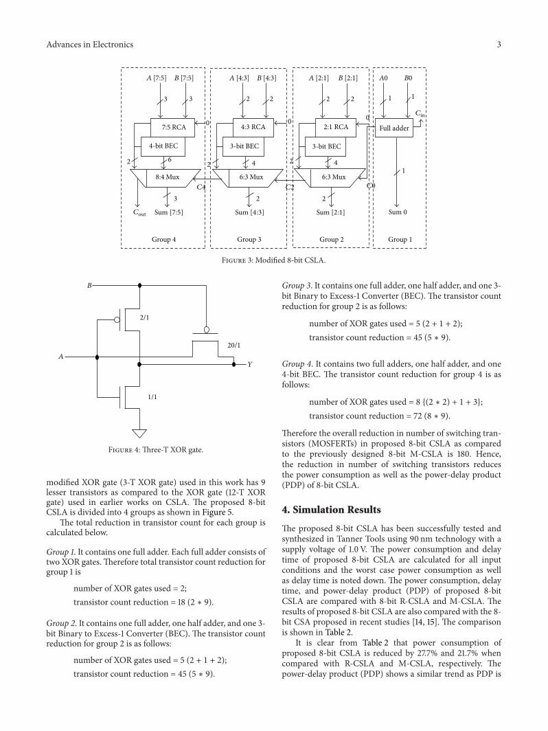
A
B
2/1
1/1
20/1
Y
Figure 4: Three-T XOR gate.
modified XOR gate (3-T XOR gate) used in this work has 9lesser transistors as compared to the XOR gate (12-T XORgate) used in earlier works on CSLA. The proposed 8-bitCSLA is divided into 4 groups as shown in Figure 5.
The total reduction in transistor count for each group iscalculated below.
Group 1. It contains one full adder. Each full adder consists oftwo XOR gates.Therefore total transistor count reduction forgroup 1 is
number of XOR gates used = 2;transistor count reduction = 18 (2 ∗ 9).
Group 2. It contains one full adder, one half adder, and one 3-bit Binary to Excess-1 Converter (BEC). The transistor countreduction for group 2 is as follows:
number of XOR gates used = 5 (2 + 1 + 2);transistor count reduction = 45 (5 ∗ 9).
Group 3. It contains one full adder, one half adder, and one 3-bit Binary to Excess-1 Converter (BEC). The transistor countreduction for group 2 is as follows:
number of XOR gates used = 5 (2 + 1 + 2);transistor count reduction = 45 (5 ∗ 9).
Group 4. It contains two full adders, one half adder, and one4-bit BEC. The transistor count reduction for group 4 is asfollows:
number of XOR gates used = 8 {(2 ∗ 2) + 1 + 3};transistor count reduction = 72 (8 ∗ 9).
Therefore the overall reduction in number of switching tran-sistors (MOSFERTs) in proposed 8-bit CSLA as comparedto the previously designed 8-bit M-CSLA is 180. Hence,the reduction in number of switching transistors reducesthe power consumption as well as the power-delay product(PDP) of 8-bit CSLA.
4. Simulation Results
The proposed 8-bit CSLA has been successfully tested andsynthesized in Tanner Tools using 90 nm technology with asupply voltage of 1.0 V. The power consumption and delaytime of proposed 8-bit CSLA are calculated for all inputconditions and the worst case power consumption as wellas delay time is noted down. The power consumption, delaytime, and power-delay product (PDP) of proposed 8-bitCSLA are compared with 8-bit R-CSLA and M-CSLA. Theresults of proposed 8-bit CSLA are also compared with the 8-bit CSA proposed in recent studies [14, 15]. The comparisonis shown in Table 2.
It is clear from Table 2 that power consumption ofproposed 8-bit CSLA is reduced by 27.7% and 21.7% whencompared with R-CSLA and M-CSLA, respectively. Thepower-delay product (PDP) shows a similar trend as PDP is
4 Advances in Electronics
Modified
Modified
ModifiedModifiedModified
ModifiedModifiedfull adder
1446 222
2C0C2C4
23
11222233
000
Group 4 Group 3 Group 2 Group 1
Sum 0
4: 3 RCA 2: 1 RCA7: 5 RCA
6: 3 Mux 6: 3 Mux8: 4 Mux
3-bit BEC3-bit BEC4-bit BEC
A0 B0
Sum [2: 1]Sum [4: 3]Sum [7: 5]
A [2:1] B [2:1]A [4:3] B [4:3]A [7:5] B [7:5]
Cout
Cin
Figure 5: Proposed 8-bit CSLA.
1.00.0
Volta
ge (V
)
1.00.0
−1.0
0 10 20 30 40 50 60 70 80 90
Time (ns)
1.00.0
Volta
ge (V
)Vo
ltage
(V)
0 10 20 30 40 50 60 70 80 90
Time (ns)
0 10 20 30 40 50 60 70 80 90
Time (ns)
1.00.0
−1.0
Volta
ge (V
)
0 10 20 30 40 50 60 70 80 90
Time (ns)
1.00.0
Volta
ge (V
)
0 10 20 30 40 50 60 70 80 90
Time (ns)
1.00.0
Volta
ge (V
)
0 10 20 30 40 50 60 70 80 90
Time (ns)
1.00.0
−1.0
Volta
ge (V
)
0 10 20 30 40 50 60 70 80 90
Time (ns)
1.00.0
−1.0
Volta
ge (V
)
0 10 20 30 40 50 60 70 80 90
Time (ns)
�(A7)
�(A6)
�(A5)
�(A4)
�(A3)
�(A2)
�(A1)
�(A0)
8-bit adder
(a)
Volta
ge (V
)
1.101.000.90
0 10 20 30 40 50 60 70 80 90
Time (ns)
1.00.0
Volta
ge (V
)Vo
ltage
(V)
0 10 20 30 40 50 60 70 80 90
Time (ns)
0 10 20 30 40 50 60 70 80 90
Time (ns)
Volta
ge (V
)
0 10 20 30 40 50 60 70 80 90
Time (ns)
0 10 20 30 40 50 60 70 80 90
Time (ns)
1.00.0
Volta
ge (V
)
0 10 20 30 40 50 60 70 80 90
Time (ns)
1.101.000.90
Volta
ge (V
)
0 10 20 30 40 50 60 70 80 90
Time (ns)
0 10 20 30 40 50 60 70 80 90
Time (ns)
1.101.000.90
1.00.0
1.101.000.90
Volta
ge (V
)
1.00.0
Volta
ge (V
)
�(B7)
�(B6)
�(B5)
�(B4)
�(B3)
�(B2)
�(B1)
�(B0)
8-bit adder
(b)
Figure 6: Postsimulation results: (a) input waveform 𝐴0to 𝐴7and (b) input waveform 𝐵
0to 𝐵7.
Advances in Electronics 5Vo
ltage
(V)
0 10 20 30 40 50 60 70 80 90
Time (ns)
1.0
0.5
0.0
Volta
ge (V
)
0 10 20 30 40 50 60 70 80 90
Time (ns)
1.0
0.5
0.0
Volta
ge (V
)
0 10 20 30 40 50 60 70 80 90
Time (ns)
1.0
0.5
0.0
Volta
ge (V
)
0 10 20 30 40 50 60 70 80 90
Time (ns)
1.5
1.0
0.5
Volta
ge (V
)
0 10 20 30 40 50 60 70 80 90
Time (ns)
1.0
0.5
0.0
8-bit adder
�(S4)
�(S3)
�(S2)
�(S1)
�(S0)
(a)
Volta
ge (V
)
0 10 20 30 40 50 60 70 80 90
Time (ns)
1.0
0.5
0.0
Volta
ge (V
)
0 10 20 30 40 50 60 70 80 90
Time (ns)
1.0
0.5
0.0
Volta
ge (V
)
0 10 20 30 40 50 60 70 80 90
Time (ns)
1.0
0.5
0.0
Volta
ge (V
)
0 10 20 30 40 50 60 70 80 90
Time (ns)
1.5
1.0
0.5
�(S7)
�(S6)
�(S5)
�(Cout)
8-bit adder
(b)
Figure 7: Postsimulation results: (a) output waveform 𝑆0to 𝑆4and (b) output waveform 𝑆
5to 𝑆7and 𝐶out.
Table 2: Comparison of various carry select adders.
Adder Total power(𝜇W) Delay (ns)
Power-delayproduct(10−15)
8-bit regularCSLA 203.9 1.719 350.5
8-bit modifiedCSLA [10] 188.4 1.958 368.5
8-bit CSLA[14] 187.58 1.976 370.8
8-bit CSA usingreversible logic [15] 180 17.2 3096
8-bit proposedCSLA 147.4 2.18 321.3
reduced by 8.3% and 12.8%when comparedwith R-CSLA andM-CSLA, respectively. Compared with the reversible logicstyle based 8-bit CSA [15], the proposed design has 18.1%reduction in power consumption and 89.6% reduction inPDP. Compared with the CSLA [14], the proposed CSLA has21.7% reduction in power consumption and 13.3% reductionin PDP.
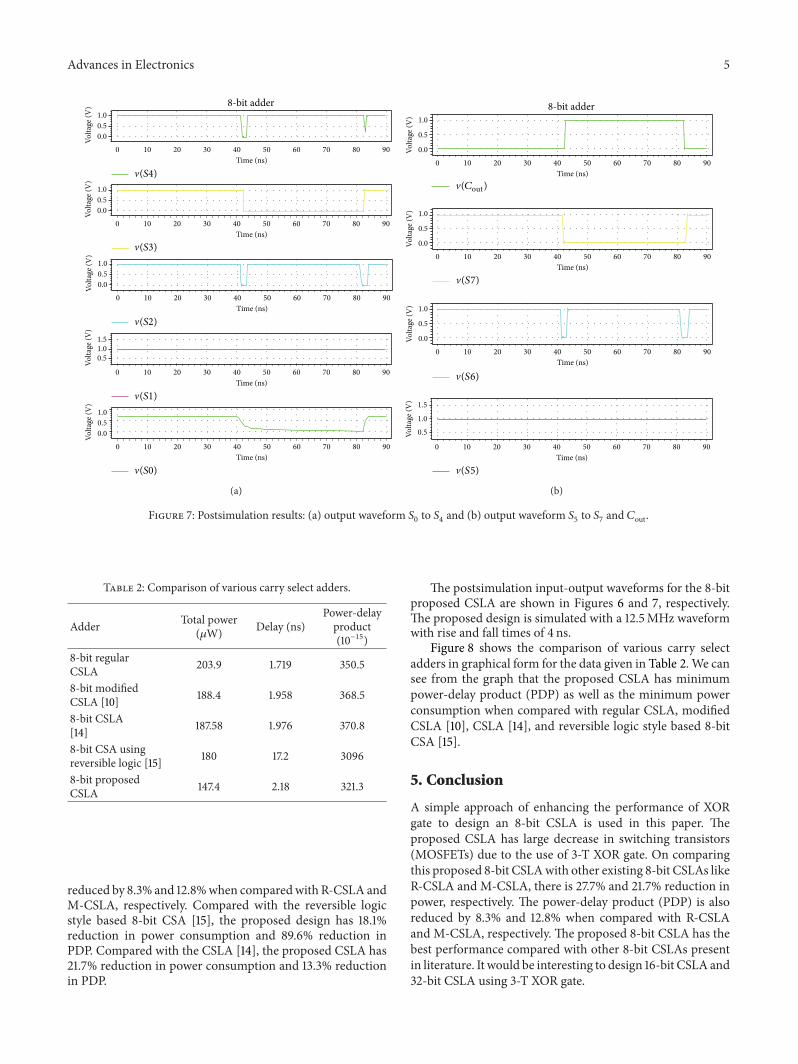
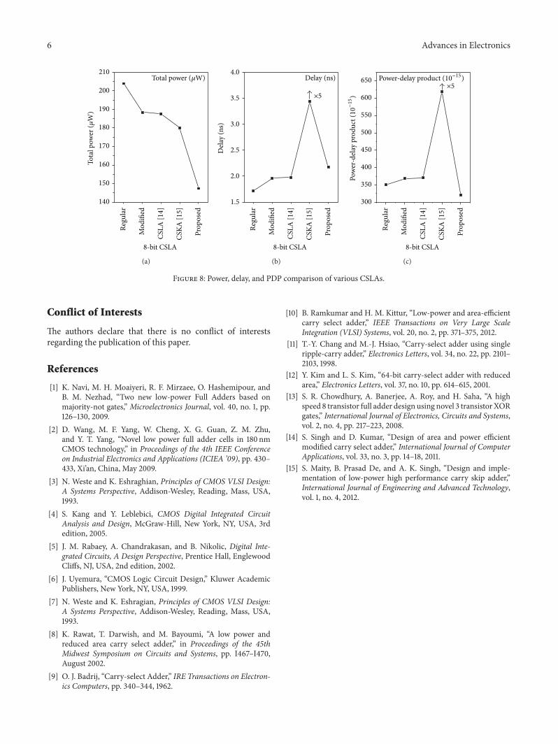
The postsimulation input-output waveforms for the 8-bitproposed CSLA are shown in Figures 6 and 7, respectively.The proposed design is simulated with a 12.5MHz waveformwith rise and fall times of 4 ns.
Figure 8 shows the comparison of various carry selectadders in graphical form for the data given in Table 2.We cansee from the graph that the proposed CSLA has minimumpower-delay product (PDP) as well as the minimum powerconsumption when compared with regular CSLA, modifiedCSLA [10], CSLA [14], and reversible logic style based 8-bitCSA [15].
5. Conclusion
A simple approach of enhancing the performance of XORgate to design an 8-bit CSLA is used in this paper. Theproposed CSLA has large decrease in switching transistors(MOSFETs) due to the use of 3-T XOR gate. On comparingthis proposed 8-bit CSLAwith other existing 8-bit CSLAs likeR-CSLA and M-CSLA, there is 27.7% and 21.7% reduction inpower, respectively. The power-delay product (PDP) is alsoreduced by 8.3% and 12.8% when compared with R-CSLAand M-CSLA, respectively. The proposed 8-bit CSLA has thebest performance compared with other 8-bit CSLAs presentin literature. It would be interesting to design 16-bit CSLA and32-bit CSLA using 3-T XOR gate.
6 Advances in Electronics
210
200
190
180
170
160
150
140
Regu
lar
Mod
ified
CSLA
[14
]
CSKA
[15
]
Prop
osed
8-bit CSLA
Tota
l pow
er (𝜇
W)
Total power (𝜇W)
(a)
4.0
3.5
3.0
2.5
2.0
1.5
Delay (ns)
Del
ay (n
s)
×5
Regu
lar
Mod
ified
CSLA
[14
]
CSKA
[15
]
Prop
osed
8-bit CSLA
(b)
650
600
Power-delay product (10−15)
Pow
er-d
elay
pro
duct
(10−15)
×5
550
500
450
400
350
300
Regu
lar
Mod
ified
CSLA
[14
]
CSKA
[15
]
Prop
osed
8-bit CSLA
(c)
Figure 8: Power, delay, and PDP comparison of various CSLAs.
Conflict of Interests
The authors declare that there is no conflict of interestsregarding the publication of this paper.
References
[1] K. Navi, M. H. Moaiyeri, R. F. Mirzaee, O. Hashemipour, andB. M. Nezhad, “Two new low-power Full Adders based onmajority-not gates,” Microelectronics Journal, vol. 40, no. 1, pp.126–130, 2009.
[2] D. Wang, M. F. Yang, W. Cheng, X. G. Guan, Z. M. Zhu,and Y. T. Yang, “Novel low power full adder cells in 180 nmCMOS technology,” in Proceedings of the 4th IEEE Conferenceon Industrial Electronics and Applications (ICIEA ’09), pp. 430–433, Xi’an, China, May 2009.
[3] N. Weste and K. Eshraghian, Principles of CMOS VLSI Design:A Systems Perspective, Addison-Wesley, Reading, Mass, USA,1993.
[4] S. Kang and Y. Leblebici, CMOS Digital Integrated CircuitAnalysis and Design, McGraw-Hill, New York, NY, USA, 3rdedition, 2005.
[5] J. M. Rabaey, A. Chandrakasan, and B. Nikolic, Digital Inte-grated Circuits, A Design Perspective, Prentice Hall, EnglewoodCliffs, NJ, USA, 2nd edition, 2002.
[6] J. Uyemura, “CMOS Logic Circuit Design,” Kluwer AcademicPublishers, New York, NY, USA, 1999.
[7] N. Weste and K. Eshragian, Principles of CMOS VLSI Design:A Systems Perspective, Addison-Wesley, Reading, Mass, USA,1993.
[8] K. Rawat, T. Darwish, and M. Bayoumi, “A low power andreduced area carry select adder,” in Proceedings of the 45thMidwest Symposium on Circuits and Systems, pp. I467–I470,August 2002.
[9] O. J. Badrij, “Carry-select Adder,” IRE Transactions on Electron-ics Computers, pp. 340–344, 1962.
[10] B. Ramkumar and H. M. Kittur, “Low-power and area-efficientcarry select adder,” IEEE Transactions on Very Large ScaleIntegration (VLSI) Systems, vol. 20, no. 2, pp. 371–375, 2012.
[11] T.-Y. Chang and M.-J. Hsiao, “Carry-select adder using singleripple-carry adder,” Electronics Letters, vol. 34, no. 22, pp. 2101–2103, 1998.
[12] Y. Kim and L. S. Kim, “64-bit carry-select adder with reducedarea,” Electronics Letters, vol. 37, no. 10, pp. 614–615, 2001.
[13] S. R. Chowdhury, A. Banerjee, A. Roy, and H. Saha, “A highspeed 8 transistor full adder design using novel 3 transistor XORgates,” International Journal of Electronics, Circuits and Systems,vol. 2, no. 4, pp. 217–223, 2008.
[14] S. Singh and D. Kumar, “Design of area and power efficientmodified carry select adder,” International Journal of ComputerApplications, vol. 33, no. 3, pp. 14–18, 2011.
[15] S. Maity, B. Prasad De, and A. K. Singh, “Design and imple-mentation of low-power high performance carry skip adder,”International Journal of Engineering and Advanced Technology,vol. 1, no. 4, 2012.

International Journal of
AerospaceEngineeringHindawi Publishing Corporationhttp://www.hindawi.com Volume 2014
RoboticsJournal of
Hindawi Publishing Corporationhttp://www.hindawi.com Volume 2014
Hindawi Publishing Corporationhttp://www.hindawi.com Volume 2014
Active and Passive Electronic Components
Control Scienceand Engineering
Journal of
Hindawi Publishing Corporationhttp://www.hindawi.com Volume 2014
International Journal of
RotatingMachinery
Hindawi Publishing Corporationhttp://www.hindawi.com Volume 2014
Hindawi Publishing Corporation http://www.hindawi.com
Journal ofEngineeringVolume 2014
Submit your manuscripts athttp://www.hindawi.com
VLSI Design
Hindawi Publishing Corporationhttp://www.hindawi.com Volume 2014
Hindawi Publishing Corporationhttp://www.hindawi.com Volume 2014
Shock and Vibration
Hindawi Publishing Corporationhttp://www.hindawi.com Volume 2014
Civil EngineeringAdvances in
Acoustics and VibrationAdvances in
Hindawi Publishing Corporationhttp://www.hindawi.com Volume 2014
Hindawi Publishing Corporationhttp://www.hindawi.com Volume 2014
Electrical and Computer Engineering
Journal of
Advances inOptoElectronics
Hindawi Publishing Corporation http://www.hindawi.com
Volume 2014
The Scientific World JournalHindawi Publishing Corporation http://www.hindawi.com Volume 2014
SensorsJournal of
Hindawi Publishing Corporationhttp://www.hindawi.com Volume 2014
Modelling & Simulation in EngineeringHindawi Publishing Corporation http://www.hindawi.com Volume 2014
Hindawi Publishing Corporationhttp://www.hindawi.com Volume 2014
Chemical EngineeringInternational Journal of Antennas and
Propagation
International Journal of
Hindawi Publishing Corporationhttp://www.hindawi.com Volume 2014
Hindawi Publishing Corporationhttp://www.hindawi.com Volume 2014
Navigation and Observation
International Journal of
Hindawi Publishing Corporationhttp://www.hindawi.com Volume 2014
DistributedSensor Networks
International Journal of