Embed Size (px)
Citation preview

Application Note 105 – JTAG In-System Programming (ISP) Implementation for the Atmel AVR Microcontroller Family Version: V1.20 – 3rd May 2010
1
Report No:
AN105 Title:
In-System Programming (ISP) of Atmel AVR FLASH Microcontroller devices using the JTAG Programming Interface Author: Date: Version Number:
John Marriott
3rd May 2010 1.20
All rights are reserved. Reproduction in whole or in part is prohibited without the prior written consent of the copyright owner. The information presented in this document does not form part of any quotation or contract, is believed to be accurate and reliable and may be changed without prior notice. No liability will be accepted by the publisher for any consequence of its use. Publication thereof does not convey nor imply any license under patent or other industrial or intellectual property rights

Application Note 105 – JTAG In-System Programming (ISP) Implementation for the Atmel AVR Microcontroller Family Version: V1.20 – 3rd May 2010
2
Application Note 105 – JTAG In-System Programming (ISP) Implementation for the Atmel AVR Microcontroller Family Version: V1.20 – 3rd May 2010
3
Contents 1.0 Introduction .................................................................................................................................... 5
1.1 Programmers supported............................................................................................................. 6 1.2 Device Support ........................................................................................................................... 7 1.3 JTAG versus SPI algorithm ........................................................................................................ 8 1.4 JTAG Algorithm Overview .......................................................................................................... 9 1.5 SPI Algorithm Overview ........................................................................................................... 10
2.0 JTAG Programming Algorithm ................................................................................................... 11 2.1 Overview .................................................................................................................................. 11 2.2 JTAG Features ......................................................................................................................... 12 2.3 JTAG PCB design / ISP cable guidelines................................................................................. 12 2.4 JTAG single-chip In-System Programming (ISP) Schematic ................................................... 13 2.5 JTAG signals – TDI, TDO, TMS, TCK...................................................................................... 14 2.6 RESET signal ........................................................................................................................... 15 2.7 JTAG-in-a-chain In-System Programming (ISP) Schematic..................................................... 16 2.8 Using the JTAG Port for both Debugging and Programming ................................................... 17 2.9 Atmel 10-way JTAG Header (JTAG Interface) ......................................................................... 18 2.9 Upgrading your Equinox Programmer to support JTAG........................................................... 20
2.9.1 Purchasing a JTAG License ............................................................................................ 20 2.9.2 How do I enable the programmer for JTAG?................................................................... 20 2.9.3 Upgrading an Epsilon5, FS2003 and FS2009 to support JTAG ...................................... 20 2.9.4 Upgrading a PPM3-MK2 and PPM4-MK1 Programmer to support JTAG ....................... 21 2.9.5 Entering the License String to upgrade your programmer ............................................... 22
3.0 Creating a JTAG Programming Project ..................................................................................... 23 3.1 Overview .................................................................................................................................. 23 3.2 Information required to create a JTAG Project ......................................................................... 23 3.3 Creating an EDS (Development project) .................................................................................. 24
3.3.1 Launching EDS and selecting a Target Device ............................................................... 24 3.3.2 Target Oscillator Settings................................................................................................. 25 3.3.3 Target System – Power Supply Settings ......................................................................... 26 3.3.4 Specifying the FLASH (Code) File ................................................................................... 27 3.3.5 Specifying the EEPROM (Data) File ................................................................................ 28 3.3.6 Launching EDS at the end of the EDS Wizard ................................................................ 29
3.4 Testing a JTAG Project in Development (EDS) Mode.............................................................. 30 3.5 JTAG Frequency ...................................................................................................................... 31 3.6 JTAG Device Chain settings .................................................................................................... 32
3.6.1 Overview.......................................................................................................................... 32 3.6.2 JTAG Chain settings ........................................................................................................ 33 3.6.3 JTAG Chain – Devices BEFORE / AFTER parameters................................................... 33 3.6.4 JTAG Chain – Instruction Bits BEFORE / AFTER parameters ........................................ 34 3.6.5 Calculating the ‘Bits Before’ value ................................................................................... 34 3.6.6 Calculating the ‘Bits After’ value ...................................................................................... 34 3.6.7 Summary of the JTAG Chain settings.............................................................................. 35
3.7 Testing JTAG communication with the Target Chip ................................................................. 36 3.8 Programming the FLASH Area.................................................................................................37 3.9 Programming the EEPROM Area............................................................................................. 38 3.10 Erasing the FLASH / EEPROM area...................................................................................... 39
3.10.1 Erasing the FLASH area................................................................................................ 39 3.10.2 Erasing the EEPROM area – special considerations..................................................... 39
3.11 Programming the Configuration Fuses................................................................................... 40 3.11.1 Overview........................................................................................................................ 40 3.11.2 Reading the Fuses from a Target Device ...................................................................... 41 3.11.3 Verifying the Fuses of a Target Device.......................................................................... 41
Application Note 105 – JTAG In-System Programming (ISP) Implementation for the Atmel AVR Microcontroller Family Version: V1.20 – 3rd May 2010
4
3.11.4 Writing the Fuses into a Target Device ......................................................................... 42 3.11.5 Using a ‘Fuse File’ to import Fuse settings into a project .............................................. 42
3.12 Programming the Security Fuses........................................................................................... 43 3.12.1 Overview........................................................................................................................ 43 3.12.2 Reading the Security Fuses from a Target Device........................................................ 44 3.12.3 Verifying the Fuses of a Target Device ......................................................................... 44 3.12.4 Writing the Security Fuses into a Target Device ........................................................... 45 3.12.5 Erasing the Security Fuses............................................................................................ 45
3.13 Internal Oscillator Calibration – Factory OSCAL Byte............................................................ 46 3.13.1 Overview........................................................................................................................ 46 3.13.2 Reading / writing the Oscillator Calibration Byte in EDS mode ..................................... 46 3.13.3 Writing the Oscillator Calibration Byte in STANDALONE mode.................................... 48
3.14 Exporting an EDS Project to a Standalone Project ................................................................ 48 4.0 Exporting / Importing Fuse Settings to / from File ................................................................... 49
4.1 Overview .................................................................................................................................. 49 4.2 Exporting the Fuse Settings to a Fuse File .............................................................................. 49 4.3 Copying the Fuses from a Target Device................................................................................. 49 4.4 Importing the Fuse Settings from a Fuse File .......................................................................... 49
5.0 Importing Fuse Settings in HEX format from AVR Studio ....................................................... 51 5.1 Overview .................................................................................................................................. 51 5.2 Finding the AVR Studio ‘Hex Fuse Values’.............................................................................. 51 5.3 Importing the AVR Studio ‘Hex Fuse Values’ into EQTools..................................................... 52 5.4 Importing the AVR Studio ‘Hex Security Fuse Values’ into EQTools....................................... 55
6.0 Creating a Standalone Programming Project ........................................................................... 59 6.1 Overview .................................................................................................................................. 59 6.2 Creating a Standalone Project from EDS (Development Mode) .............................................. 59 6.3 Add Project File to a new Project Collection ............................................................................ 59 6.4 Uploading a Project to a programmer ...................................................................................... 60 6.5 Re-testing a Project in EDS (Development mode)................................................................... 61

Application Note 105 – JTAG In-System Programming (ISP) Implementation for the Atmel AVR Microcontroller Family Version: V1.20 – 3rd May 2010
5
1.0 Introduction This application note describes how to develop and implement In-System Programming (ISP) support for the Atmel AVR microcontroller family using the ‘JTAG Programming Interface’. The document details how to make a JTAG ‘Programming Project’ which will operate on any Equinox ISP programmer. A full description of all connection method required to implement JTAG In-System Programming (ISP) of the Atmel AT90USB, AT90CAN and ATmega AVR FLASH Microcontroller is also discussed. Please note:
• Programming of the Atmel AVR microcontroller family using the ‘SPI Programming Interface’ is covered in Application Note – AN101.
• Programming of the Atmel XMEGA AVR microcontroller family using the JTAG and PDI interfaces is covered in Application Note – AN127.
• The Atmel ATtiny AVR Family features both a ‘Low Voltage’ and ‘High Voltage’ Serial Programming Modes. Please refer to Application Note - AN104 for further details.
• Programming of the Atmel AT91SAM7 microcontroller family using the ‘JTAG Programming Interface’ is covered in Application Note – AN122.
Application Note 105 – JTAG In-System Programming (ISP) Implementation for the Atmel AVR Microcontroller Family Version: V1.20 – 3rd May 2010
6
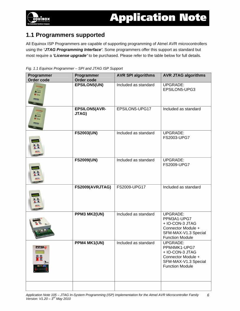
1.1 Programmers supported All Equinox ISP Programmers are capable of supporting programming of Atmel AVR microcontrollers using the ‘JTAG Programming Interface’. Some programmers offer this support as standard but most require a ‘License upgrade’ to be purchased. Please refer to the table below for full details.
Fig. 1.1 Equinox Programmer – SPI and JTAG ISP Support
Programmer Order code
Programmer Order code
AVR SPI algorithms AVR JTAG algorithms
EPSILON5(UN)
Included as standard UPGRADE: EPSILON5-UPG3
EPSILON5(AVR-JTAG)
EPSILON5-UPG17 Included as standard
FS2003(UN)
Included as standard UPGRADE: FS2003-UPG7
FS2009(UN)
Included as standard UPGRADE: FS2009-UPG7
FS2009(AVRJTAG)
FS2009-UPG17 Included as standard
PPM3 MK2(UN)
Included as standard UPGRADE: PPM3A1-UPG7 + IO-CON-3 JTAG Connector Module + SFM-MAX-V1.3 Special Function Module
PPM4 MK1(UN)
Included as standard UPGRADE: PPM4MK1-UPG7 + IO-CON-3 JTAG Connector Module + SFM-MAX-V1.3 Special Function Module
Application Note 105 – JTAG In-System Programming (ISP) Implementation for the Atmel AVR Microcontroller Family Version: V1.20 – 3rd May 2010
7
ISPnano Series I / II / III (ATE)
UPGRADE ISPnano-UPG17
UPGRADE ISPnano-UPG17
Key:
• UPGRADE – Chargeable license upgrade required 1.2 Device Support Please refer to the latest Device Support List for the devices which are currently supported by the Equinox range of programmers. This can be found:
1. As a Download available on the website: - Click on the Downloads tab. - Under ‘Download Type’ choose Device Support Lists / Release notes then click
Search. 2. Browsing on the Device Support tab under each product. 3. In the latest version of EQTools:
- Select EQTools. Go to <Programmer >Create a Device Support. - All programmers and devices supported are listed in this document. - You will need the most recent EQ-Tools build version – please refer to the website for
further details. Please note:
• As a rule of thumb, only Atmel Atmega AVR devices with 16k bytes of FLASH or greater will feature the JTAG Programming Interface.
• Some ATmega devices such as the ATmega8(L) and ATmega161(L) do not have a JTAG port and so cannot support JTAG programming.
• Devices with greater than 128kb of FLASH memory require a firmware upgrade to version 3.01 or above in order to support programming of the upper 128kb.
• It is possible to program devices connected in a ‘JTAG Chain’ using firmware 3.05 or above. • Please see Application Note – AN112 for instructions on updating your programmer
firmware.
Application Note 105 – JTAG In-System Programming (ISP) Implementation for the Atmel AVR Microcontroller Family Version: V1.20 – 3rd May 2010
8
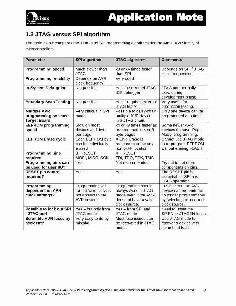
1.3 JTAG versus SPI algorithm The table below compares the JTAG and SPI programming algorithms for the Atmel AVR family of microcontrollers. Parameter
SPI algorithm JTAG algorithm Comments
Programming speed Much slower than JTAG
x3 or x4 times faster than SPI
Depends on SPI / JTAG clock frequencies
Programming reliability Depends on AVR clock frequency
Very good
In-System Debugging Not possible Yes – use Atmel JTAG-ICE debugger
JTAG port normally used during development phase
Boundary Scan Testing Not possible Yes – requires external JTAG tester
Very useful for production testing.
Multiple AVR programming on same Target Board
Very difficult in SPI mode
Possible to daisy-chain multiple AVR devices in a JTAG chain.
Only one device can be programmed at a time.
EEPROM programming speed
Slow on most devices as 1 byte per page
x4 or x8 times faster as programmed in 4 or 8 byte pages
Some newer AVR devices do have ‘Page Mode’ programming.
EEPROM Erase cycle Each EEPROM byte can be individually erased
A Chip Erase is required to erase any non 0xFF location
Cannot use JTAG mode to re-program EEPROM without erasing FLASH.
Programming pins required
3 + RESET MOSI, MISO, SCK
4 + RESET TDI, TDO, TCK, TMS
Programming pins can be used for user I/O?
Yes Not recommended Try not to put other components on pins.
RESET pin control required?
Yes Yes The RESET pin is essential for SPI and JTAG operation.
Programming dependent on AVR clock settings?
Programming will fail if a valid clock is not applied to the AVR device.
Programming should always work in JTAG mode even if the AVR does not have a valid clock source.
In SPI mode, an AVR device can be rendered no longer programmable by selecting an incorrect clock source.
Possible to lock out SPI / JTAG port
Yes – but only from JTAG mode
Yes – from SPI and JTAG mode
Need to unset the SPIEN or JTAGEN fuses
Scramble AVR fuses by accident?
Very easy to do by mistake!!!
Most fuse issues can be recovered in JTAG mode.
Use JTAG mode to recover a device with scrambled fuses.

Application Note 105 – JTAG In-System Programming (ISP) Implementation for the Atmel AVR Microcontroller Family Version: V1.20 – 3rd May 2010
9
1.4 JTAG Algorithm Overview The JTAG algorithm provides a method of performing high-speed programming of an Atmel Atmega AVR microcontroller. The same JTAG port can also be used for on-chip debugging of code using the Atmel JTAG-ICE Debugger. The advantages and disadvantages of the JTAG algorithm are detailed below. Advantages
• The JTAG algorithm is approximately 3-4 times faster at programming compared to the SPI algorithm.
• The programming time using JTAG for the EEPROM is significantly faster than the SPI algorithm because in JTAG mode a ‘Page’ of EEPROM is programmed at a time rather than a single byte. Each byte may take e.g. 9ms to program in SPI mode, where as a whole page of e.g. 4 bytes may take 9ms to program in JTAG mode.
• The JTAG algorithm uses the same ‘JTAG Port’ as the Atmel JTAG-ICE Debugger. This means that the same port can be used for both debugging during the development phase and also programming during the production phase of the product.
• With the JTAG algorithm, the programming clock is supplied by the programmer and JTAG logic inside the Target AVR device does not require any other clocking. This means that the chip is not dependent on the settings of the ‘Clock Selection Fuses’ in JTAG Mode.
• In JTAG mode is it possible to change the ‘Clock Selection Fuses’ to any value and still program the chip. (with the exception of the ‘JTAGEN’ Fuse)
• It is possible to use the JTAG port of the Target Microcontroller to perform in-circuit testing of the microcontroller and surrounding circuitry. This testing is performed by shifting Test Data through the JTAG port of the Target Microcontroller. A JTAG Test System is required to perform this testing. It is not supported by any Equinox Programmer or the Atmel JTAG ICE.
• It is possible to daisy-chain multiple JTAG devices on the JTAG bus in a so-called ‘JTAG Chain’ and then select to program a particular device in the chain. This functionality is now supported by Equinox programmers running firmware 3.05 and above.
Disadvantages
• The JTAG Programming Interface uses 5 pins: TCK, TDI, TDO, TMS and RESET. • The JTAG pins of the microcontroller are not designed for off-board use and should not be
shared with any other circuitry on Target Board. This means that the JTAG port pins must be dedicated for programming / debugging.
• In JTAG mode the EEPROM is divided into ‘Pages’ rather than ‘Single Bytes’. It is therefore more complicated to program a single byte in the EEPROM as the entire page (usually 4 or 8 bytes) must be read back and then the single byte overlaid on top of this data and finally the entire page is then re-programmed back into the EEPROM.
• In JTAG Mode, it is not possible to re-program any location in the EEPROM which is not 0xFF without first performing a Chip Erase operation. This means that if the EEPROM already contains any data, it is not possible to re-program this data without erasing the entire chip first.
Application Note 105 – JTAG In-System Programming (ISP) Implementation for the Atmel AVR Microcontroller Family Version: V1.20 – 3rd May 2010
10
1.5 SPI Algorithm Overview The SPI algorithm is a simple 3-wire interface which can be used to program most AVR Microcontrollers. The advantages and disadvantages of this algorithm are detailed below. Advantages
• The SPI algorithm is supported by almost all Atmel AVR microcontrollers including AT90S, AT90CANxxx, ATtiny and ATmega devices. This means that the same Programming Interface can be used on any products containing any AVR microcontroller.
• The SPI Programming Interface uses only 3 SPI pins (MOSI, MISO, SCK) and the RESET pin. • The SPI pins can be used to drive other circuitry such as LED’s and switches on the Target
Board as well as being used for ISP purposes. However, this will require careful design on the Target Board to ensure that the programming signals are not compromised.
• In SPI Mode, it is possible to reprogram a single byte of the EEPROM area without having to perform a Chip Erase first.
• The SPI algorithms are supported as standard on all Equinox ISP Programmers. Disadvantages
• In general terms, the SPI algorithm is 3-4 times slower than the JTAG algorithm. • When using the SPI algorithm, the clock used during programming is supplied from either the
AVR Internal RC Oscillator or from an external crystal / resonator. The programming SPI speed is completely dependent on the speed of this oscillator.
• If the oscillator speed is slow, then the maximum SPI speed is seriously limited and the overall programming will be very slow.
• If the Clock Selection Fuses are incorrectly programmed in SPI mode, then the chip may no longer have a valid oscillator and so will not respond to the programmer. This can render the chip unprogrammable except by physically removing it from the Target Board and using either a JTAG or Parallel programmer to resurrect the correct Fuse Settings.

Application Note 105 – JTAG In-System Programming (ISP) Implementation for the Atmel AVR Microcontroller Family Version: V1.20 – 3rd May 2010
11
2.0 JTAG Programming Algorithm 2.1 Overview The ‘JTAG Programming Interface’ provides a method for both In-System Debugging (ISD) and In-System Programming (ISP) of Atmel ATmega AVR Microcontrollers. It uses an industry-standard set of signals to provide the connection between the programmer / debugger and the AVR microcontroller. However, the actual JTAG Header (connector) used by Atmel and Equinox is specific to Atmel AVR JTAG programming and will not match JTAG connectors for JTAG devices from other manufacturers.
In the development environment…… …..The JTAG Interface can be used for In-System Debugging of the code running on the actual Target System. This method of operation requires the use of the Atmel ‘JTAG-ICE MK1’ or ‘JTAG-ICE MK2’ debugger to program firmware into the FLASH of the target AVR microcontroller. Once the code is downloaded into FLASH, it is then possible to execute and debug this code under PC control. The debugger Software (AVR Studio) allows you to set breakpoints in the code, read / write memory locations, look at register contents etc. In the production environment….. ……The JTAG Interface can be use for high-speed In-System Programming (ISP) of the Target AVR Microcontroller. This method of operation requires the use of any Equinox ISP Programmer which has been enabled to support the ‘AVR JTAG’ algorithms. The Equinox ISP Programmer range supports high-speed In-System Programming (ISP) of a single or multiple Atmel AVR microcontrollers on a Target Board using the 4-wire JTAG inerface. Support has now been added for programming of any Atmel AVR microcontroller when connected as part of a ‘JTAG Chain’. This mode allows multiple JTAG devices to be in-system programmed using a single JTAG bus.
Application Note 105 – JTAG In-System Programming (ISP) Implementation for the Atmel AVR Microcontroller Family Version: V1.20 – 3rd May 2010
12
2.2 JTAG Features • Fast Programming speeds • Simple 4-wire JTAG bus connection + RESET signal • JTAG programming does not depend on the AVR oscillator frequency so JTAG programming
will always work • JTAG interface is compatible with the Atmel JTAG-ICE MK2 In-System Debugger so same
interface can be used for development and production. • Both single microcontroller and ‘JTAG-in-a-chain’ implementations are supported
2.3 JTAG PCB design / ISP cable guidelines The following guidelines are provided for designing an ‘AVR based Target Board’ which is to be programmed via the JTAG interface.
• Proper decoupling - Make sure the AVR microcontroller is well decoupled. • No JTAG in-line resistors - Avoid placing any resistors in the JTAG lines TDO, TDI, TCK,
TMS as this can skew the waveforms so the JTAG clock is not sampled correctly. • No JTAG capacitors - Avoid placing any capacitors from any of the JTAG lines to 0V as this
will slug the waveforms and probably stop JTAG working reliably. • JTAG pull-up resistors - It is recommended that either the Target Board or the Test Fixture
has pull-ups e.g. 47k ohm on the JTAG signal lines. (The programmer does not have any pull-ups)
• RESET pin connection - Make sure that the RESET pin of the target AVR microcontroller is brought out to the programming header. It is essential that the programmer can control the RESET pin of the AVR device !!!
• Cable length - Keep the cable length between the Target Board and the programmer as short as possible. e.g. no more than 15cm in length.
• JTAG relays etc - Do not use any relays or electronics analogue switches in the JTAG signal lines if at all possible.
Application Note 105 – JTAG In-System Programming (ISP) Implementation for the Atmel AVR Microcontroller Family Version: V1.20 – 3rd May 2010
13
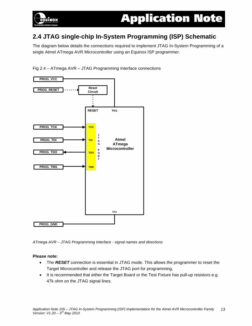
2.4 JTAG single-chip In-System Programming (ISP) Schematic The diagram below details the connections required to implement JTAG In-System Programming of a single Atmel ATmega AVR Microcontroller using an Equinox ISP programmer. Fig 2.4 – ATmega AVR – JTAG Programming Interface connections
TCK
TDI
TDO
TMS
Vcc
Vss
RESET
PROG_RESET
PROG_TCK
PROG_TDI
PROG_TDO
PROG_TMS
AtmelATmega
Microcontroller
PROG_VCC
PROG_GND
ResetCircuit
JTAG
PORT
ATmega AVR – JTAG Programming Interface - signal names and directions
Please note:
• The RESET connection is essential in JTAG mode. This allows the programmer to reset the Target Microcontroller and release the JTAG port for programming.
• It is recommended that either the Target Board or the Test Fixture has pull-up resistors e.g. 47k ohm on the JTAG signal lines.
Application Note 105 – JTAG In-System Programming (ISP) Implementation for the Atmel AVR Microcontroller Family Version: V1.20 – 3rd May 2010
14
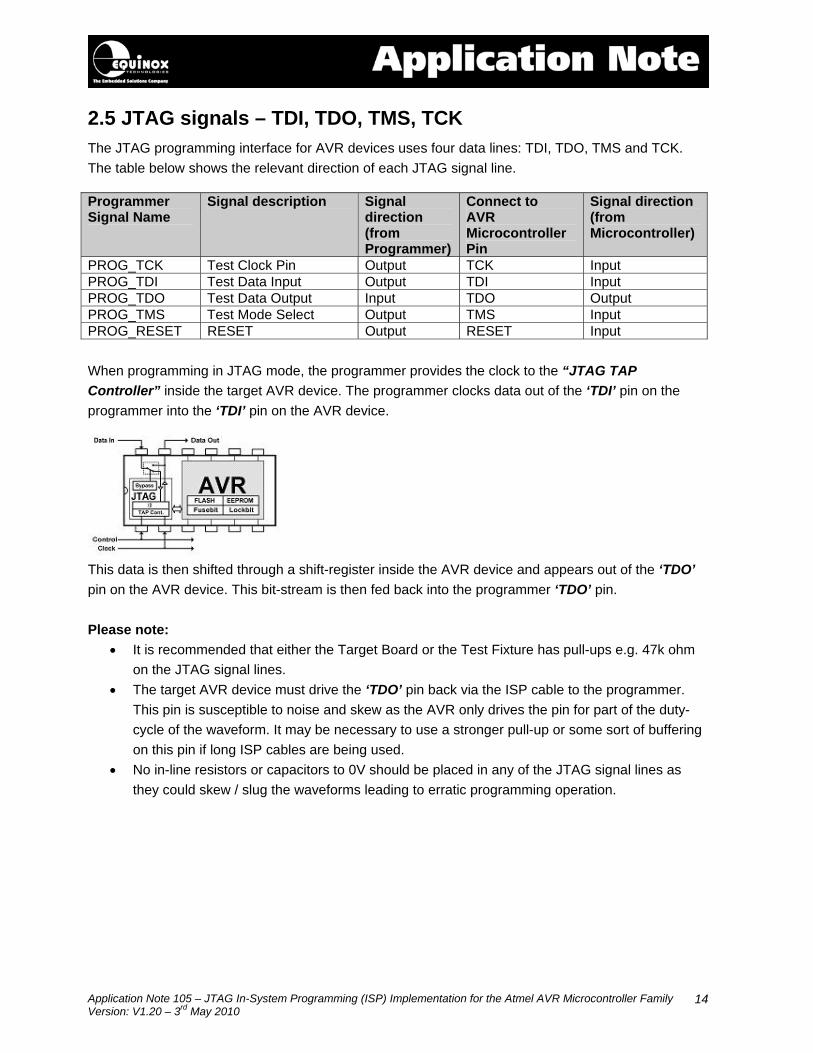
2.5 JTAG signals – TDI, TDO, TMS, TCK The JTAG programming interface for AVR devices uses four data lines: TDI, TDO, TMS and TCK. The table below shows the relevant direction of each JTAG signal line. Programmer Signal Name
Signal description Signal direction (from Programmer)
Connect to AVR Microcontroller Pin
Signal direction (from Microcontroller)
PROG_TCK Test Clock Pin Output TCK Input PROG_TDI Test Data Input Output TDI Input PROG_TDO Test Data Output Input TDO Output PROG_TMS Test Mode Select Output TMS Input PROG_RESET RESET Output RESET Input When programming in JTAG mode, the programmer provides the clock to the “JTAG TAP Controller” inside the target AVR device. The programmer clocks data out of the ‘TDI’ pin on the programmer into the ‘TDI’ pin on the AVR device.
This data is then shifted through a shift-register inside the AVR device and appears out of the ‘TDO’ pin on the AVR device. This bit-stream is then fed back into the programmer ‘TDO’ pin. Please note:
• It is recommended that either the Target Board or the Test Fixture has pull-ups e.g. 47k ohm on the JTAG signal lines.
• The target AVR device must drive the ‘TDO’ pin back via the ISP cable to the programmer. This pin is susceptible to noise and skew as the AVR only drives the pin for part of the duty-cycle of the waveform. It may be necessary to use a stronger pull-up or some sort of buffering on this pin if long ISP cables are being used.
• No in-line resistors or capacitors to 0V should be placed in any of the JTAG signal lines as they could skew / slug the waveforms leading to erratic programming operation.

Application Note 105 – JTAG In-System Programming (ISP) Implementation for the Atmel AVR Microcontroller Family Version: V1.20 – 3rd May 2010
15
2.6 RESET signal When programming Atmel AVR devices using the JTAG Interface, it is imperative that the programmer can control the RESET pin of the target AVR microcontroller. It does not matter if the RESET signal from the programmer goes through other logic on the Target Board, as long as the programmer is capable of forcing the RESET pin LOW when commencing a JTAG programming operation. The reasons for requiring control of the RESET pin are as follows:
• If any user firmware which is programmed into the target AVR device writes to any of the JTAG pins or sets up the ‘Data Direction Registers’ of the JTAG port incorrectly, then the JTAG port will no longer operate correctly and entering JTAG programming mode will fail.
• If any user firmware which is programmed into the target AVR device happens to execute the AVR instruction to disable the JTAG port (usually for power consumption reasons), then the programmer will not be able to enter JTAG programming mode.
• The programmer must assert the RESET pin of the target AVR microcontroller LOW when commencing a JTAG programming operation. This forces the AVR device to stop running firmware and releases / resets the JTAG port so the programmer can communicate with it.
Warning!
• Any AVR Target System which does not allow control of the RESET pin may be programmable once only via JTAG and then all subsequent attempts to enter JTAG programming mode may fail.
• Once the target AVR device is in JTAG mode, the RESET pin will have no effect until JTAG mode has been exited. This will hold the AVR device in reset so it cannot execute code.
Application Note 105 – JTAG In-System Programming (ISP) Implementation for the Atmel AVR Microcontroller Family Version: V1.20 – 3rd May 2010
16
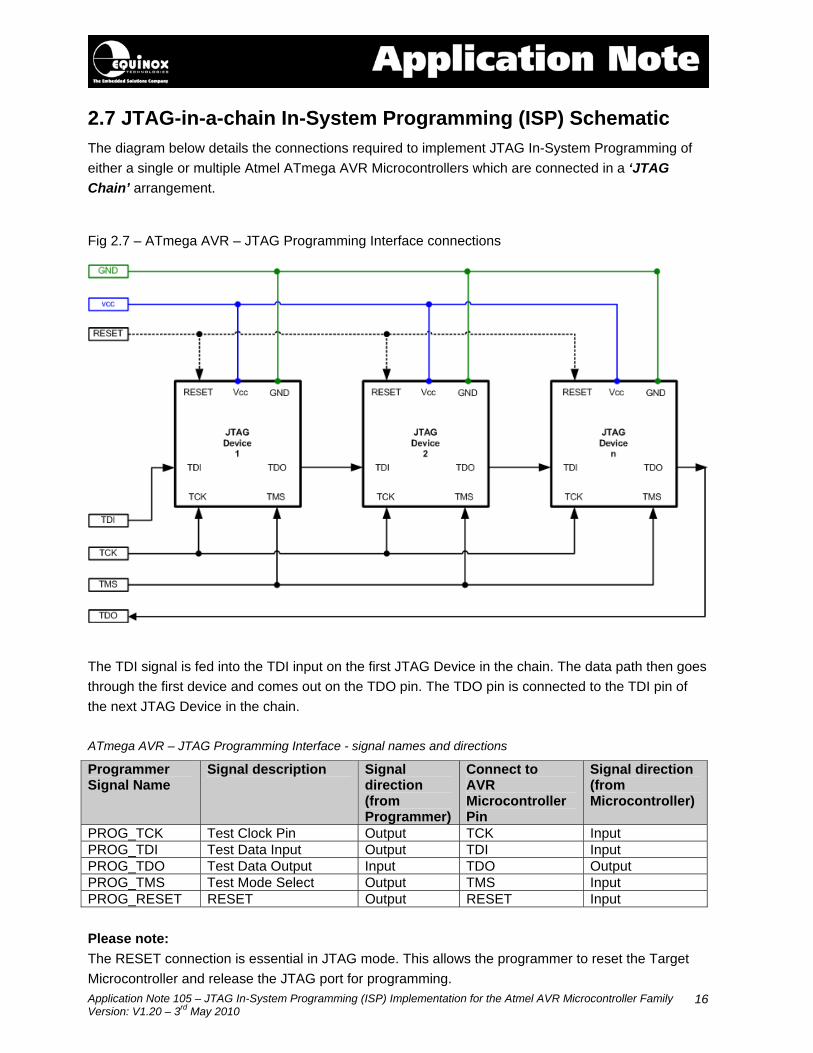
2.7 JTAG-in-a-chain In-System Programming (ISP) Schematic The diagram below details the connections required to implement JTAG In-System Programming of either a single or multiple Atmel ATmega AVR Microcontrollers which are connected in a ‘JTAG Chain’ arrangement. Fig 2.7 – ATmega AVR – JTAG Programming Interface connections
The TDI signal is fed into the TDI input on the first JTAG Device in the chain. The data path then goes through the first device and comes out on the TDO pin. The TDO pin is connected to the TDI pin of the next JTAG Device in the chain. ATmega AVR – JTAG Programming Interface - signal names and directions
Programmer Signal Name
Signal description Signal direction (from Programmer)
Connect to AVR Microcontroller Pin
Signal direction (from Microcontroller)
PROG_TCK Test Clock Pin Output TCK Input PROG_TDI Test Data Input Output TDI Input PROG_TDO Test Data Output Input TDO Output PROG_TMS Test Mode Select Output TMS Input PROG_RESET RESET Output RESET Input Please note: The RESET connection is essential in JTAG mode. This allows the programmer to reset the Target Microcontroller and release the JTAG port for programming.

Application Note 105 – JTAG In-System Programming (ISP) Implementation for the Atmel AVR Microcontroller Family Version: V1.20 – 3rd May 2010
17
2.8 Using the JTAG Port for both Debugging and Programming The JTAG port of an ATmega AVR Microcontroller can be used for both debugging and programming purposes. The Equinox ‘JTAG ISP Header’ pin-out found on all Equinox ISP Programmers uses the same pins as the Atmel ‘JTAG ICE MK1 / MK2’ Debugger so it is possible to use the same connector / cabling for both programming and debugging. Fig. 2.7 JTAG ISP 10-way IDC Header
Atmel 10-way JTAG IDC Header Atmel JTAG ICE MK1 or MK2
Equinox ISP Programmer
Important notes: 1. RESET pin connection The RESET pin of the AVR Microcontroller must be brought out to the ISP Header. It is not actually required for the JTAG algorithm as the control of programming initiated via a JTAG command. However, the Equinox programmer / Atmel JTAG-ICE can use the RESET pin to RESET the Target AVR microcontroller to ensure that the AVR JTAG port is not driving any I/O pins which could cause contention during programming. The JTAG-ICE also needs control of the RESET pin to force the AVR microcontroller to execute code when in debugging mode.
Application Note 105 – JTAG In-System Programming (ISP) Implementation for the Atmel AVR Microcontroller Family Version: V1.20 – 3rd May 2010
18
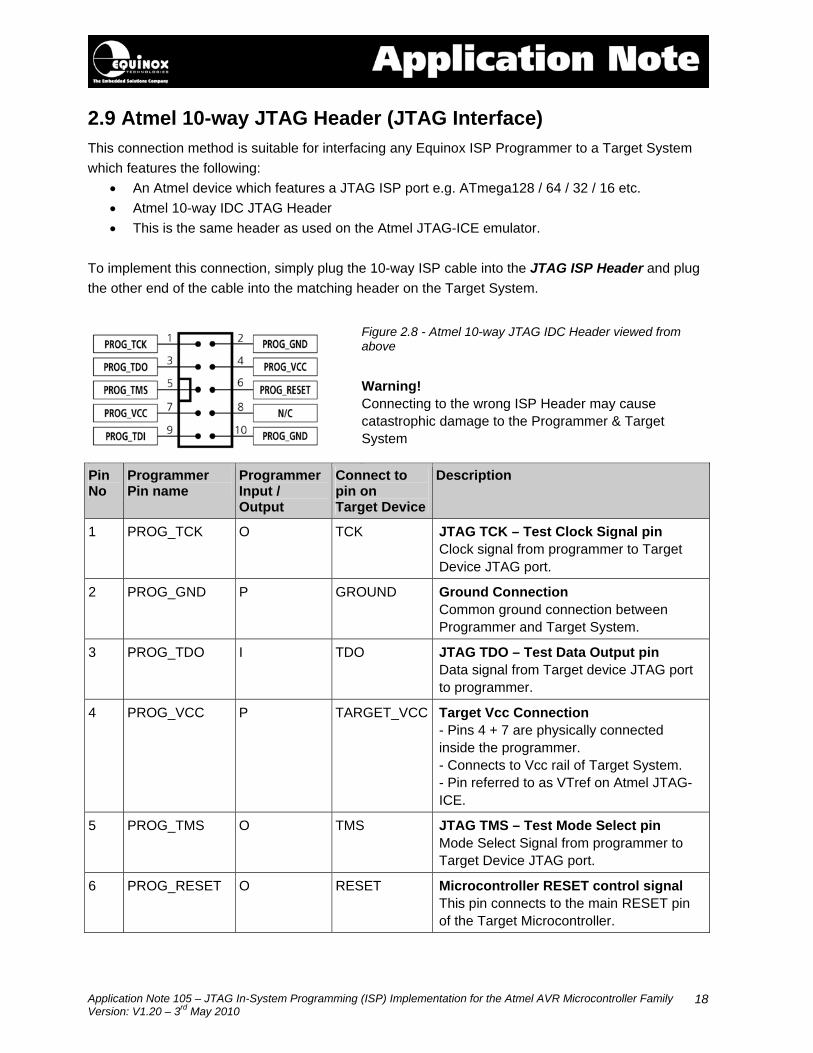
2.9 Atmel 10-way JTAG Header (JTAG Interface) This connection method is suitable for interfacing any Equinox ISP Programmer to a Target System which features the following:
• An Atmel device which features a JTAG ISP port e.g. ATmega128 / 64 / 32 / 16 etc. • Atmel 10-way IDC JTAG Header • This is the same header as used on the Atmel JTAG-ICE emulator.
To implement this connection, simply plug the 10-way ISP cable into the JTAG ISP Header and plug the other end of the cable into the matching header on the Target System.
Figure 2.8 - Atmel 10-way JTAG IDC Header viewed from above
Warning! Connecting to the wrong ISP Header may cause catastrophic damage to the Programmer & Target System
Pin No
Programmer Pin name
Programmer Input / Output
Connect to pin on Target Device
Description
1 PROG_TCK O TCK JTAG TCK – Test Clock Signal pin Clock signal from programmer to Target Device JTAG port.
2 PROG_GND P GROUND Ground Connection Common ground connection between Programmer and Target System.
3 PROG_TDO I TDO JTAG TDO – Test Data Output pin Data signal from Target device JTAG port to programmer.
4 PROG_VCC P TARGET_VCC
Target Vcc Connection - Pins 4 + 7 are physically connected inside the programmer. - Connects to Vcc rail of Target System. - Pin referred to as VTref on Atmel JTAG-ICE.
5 PROG_TMS O TMS JTAG TMS – Test Mode Select pin Mode Select Signal from programmer to Target Device JTAG port.
6 PROG_RESET O RESET Microcontroller RESET control signal This pin connects to the main RESET pin of the Target Microcontroller.

Application Note 105 – JTAG In-System Programming (ISP) Implementation for the Atmel AVR Microcontroller Family Version: V1.20 – 3rd May 2010
19
7 PROG_VCC P TARGET_VCC Target Vcc Connection
- See pin 4 - Pins 4 + 7 are physically connected inside the programmer.
8 N/C O N/C Not Connected
9 PROG_TDI O TDI JTAG TDI – Test Data Input pin Data signal from programmer to Target Device JTAG port.
10 PROG_GND P GROUND Ground Connection Common ground connection between PROGRAMMER and Target System.
Key O - Output from programmer to Target Device I - Input to programmer from Target Device P - Passive e.g. GROUND and power rails N/C - Not connected
Application Note 105 – JTAG In-System Programming (ISP) Implementation for the Atmel AVR Microcontroller Family Version: V1.20 – 3rd May 2010
20
2.9 Upgrading your Equinox Programmer to support JTAG The AVR JTAG algorithms are not supported as standard on any Equinox programmers (for exceptions – see below*). It is necessary to purchase a ‘License Upgrade’ for AVR JTAG support from Equinox. Equinox will then send you a ‘JTAG Upgrade License String’ which will upgrade your programmer to support JTAG programming. Please note the following ‘Standalone programmer’ and ‘Bundle’ options have the AVR JTAG license pre-installed, therefore these instructions are not necessary:
• Epsilon5(AVR-JTAG) • EPS-AVRJTAG-BUNDLE • FS2009(AVR-JTAG)
2.9.1 Purchasing a JTAG License All Equinox ISP programmers require the purchase of a ‘License Upgrade’ to enable JTAG support. Please see the table in section 1.1 for the relevant upgrade for your programmer. 2.9.2 How do I enable the programmer for JTAG? To enable your programmer to support JTAG ISP programming, please purchase the relevant JTAG Upgrade from Equinox or an Equinox distributor:
1. If you purchase the upgrade directly from Equinox • Equinox will email you a ‘JTAG License String’. • This string can be entered directly into the <Enter License> screen in EQTools.
2. If you purchase the upgrade from a distributor
• The distributor will send you the Upgrade Pack by courier. • Within the Upgrade Pack you will find an Upgrade Form with a Code String on it. • Email this Code String plus your programmer Serial Number to support@equinox-
tech.com • Equinox will then send you a ‘JTAG License String’ which is keyed to your programmer
Serial Number. • This string can be entered directly into the <Enter License> screen in EQTools.
2.9.3 Upgrading an Epsilon5, FS2003 and FS2009 to support JTAG To upgrade an Epsilon5, FS2003 or FS2009 programmer to support JTAG, please follow the steps below:
• Order An AVR JTAG License from Equinox • Enter the ‘JTAG Upgrade License String’ given to you by Equinox into EQTools – see
section 2.9.5 below. • Make sure you have the required version of Programmer Firmware to support the device you
wish to program. • Plug the 10-way ISP cable supplied with the programmer into the ‘J8 – JTAG-10’ ISP Header
on the programmer. • Connect the other end of the 10-way ISP cable to the JTAG port on your Target Board • You are now ready to program a Target AVR Chip via JTAG.
Application Note 105 – JTAG In-System Programming (ISP) Implementation for the Atmel AVR Microcontroller Family Version: V1.20 – 3rd May 2010
21
2.9.4 Upgrading a PPM3-MK2 and PPM4-MK1 Programmer to support JTAG To upgrade a PPM3-MK2 or PPM4-MK1 programmer to support JTAG, please follow the steps below:
• Order a ‘PPM3-MK2 / PPM4-MK1 JTAG upgrade’ from Equinox Technologies • Enter the ‘JTAG Upgrade License String’ given to you by Equinox into EQTools – see section
2.9.5 below. • The JTAG upgrade also includes a new ‘I/O Connector Module’ for the PPM3-MK2 and PPM4-
MK1 called the ‘I/O-CON-3’. This module has a JTAG 10-way header which has the same pin-out as the JTAG-ICE.
• It also includes the High Speed / High Current Special Function Module ‘EQ-SFM-MAX-V1.3’. This significantly reduces the overall programming times for many high capacity devices. For full instructions on fitting this module please refer to Application Note AN115 provided with your upgrade
• Make sure you have the required version of Programmer Firmware to support the device you wish to program.
• Plug the ‘I/O-CON-3’ module into the programmer. • Plug the 10-way ISP cable supplied with the programmer into the ‘JTAG’ ISP Header on the
‘I/O-CON-3’ module. • Connect the other end of the 10-way ISP cable to the JTAG port on your Target Board • You are now ready to program a Target Chip via JTAG
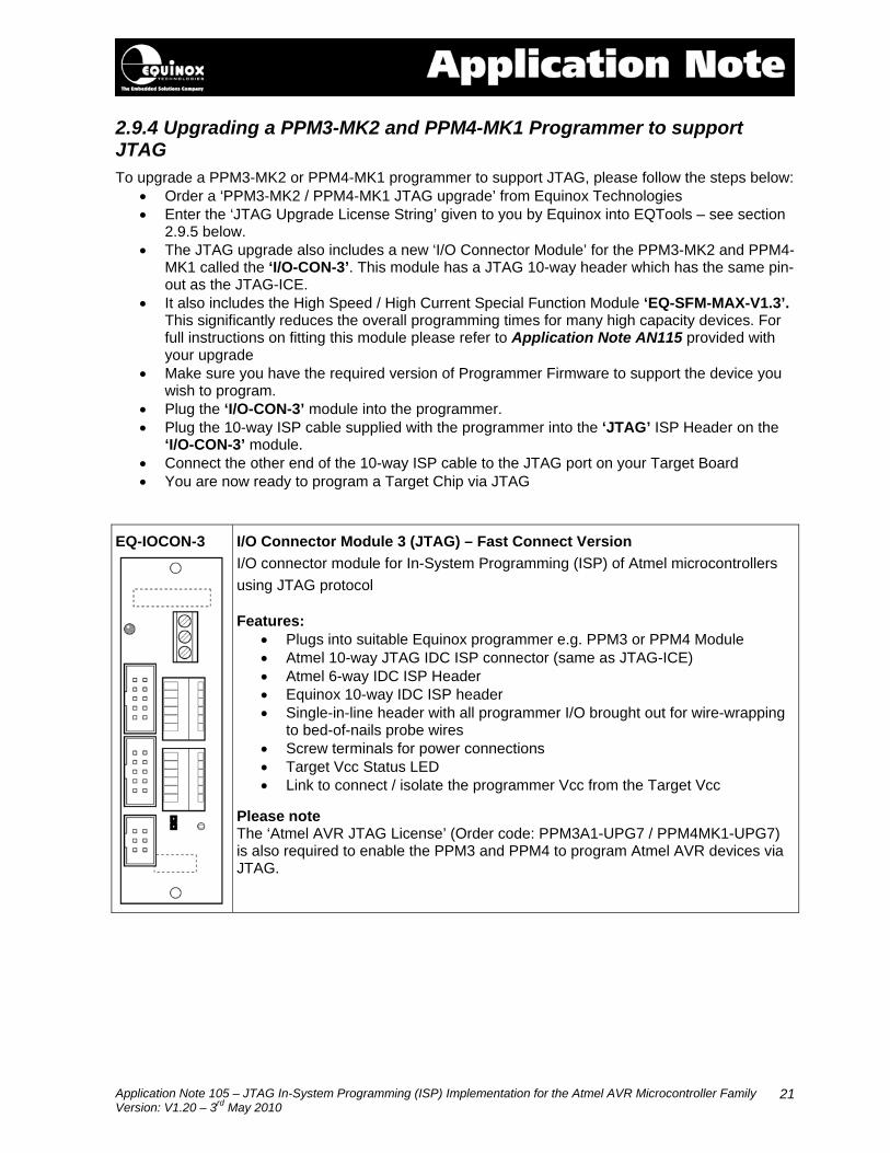
EQ-IOCON-3
I/O Connector Module 3 (JTAG) – Fast Connect Version I/O connector module for In-System Programming (ISP) of Atmel microcontrollers using JTAG protocol Features:
• Plugs into suitable Equinox programmer e.g. PPM3 or PPM4 Module • Atmel 10-way JTAG IDC ISP connector (same as JTAG-ICE) • Atmel 6-way IDC ISP Header • Equinox 10-way IDC ISP header • Single-in-line header with all programmer I/O brought out for wire-wrapping
to bed-of-nails probe wires • Screw terminals for power connections • Target Vcc Status LED • Link to connect / isolate the programmer Vcc from the Target Vcc
Please note The ‘Atmel AVR JTAG License’ (Order code: PPM3A1-UPG7 / PPM4MK1-UPG7) is also required to enable the PPM3 and PPM4 to program Atmel AVR devices via JTAG.
Application Note 105 – JTAG In-System Programming (ISP) Implementation for the Atmel AVR Microcontroller Family Version: V1.20 – 3rd May 2010
22
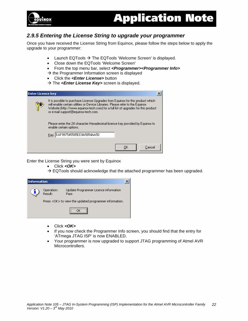
2.9.5 Entering the License String to upgrade your programmer Once you have received the License String from Equinox, please follow the steps below to apply the upgrade to your programmer:
• Launch EQTools The EQTools ‘Welcome Screen’ is displayed. • Close down the EQTools ‘Welcome Screen’ • From the top menu bar, select <Programmer><Programmer Info>
the Programmer Information screen is displayed • Click the <Enter License> button
The <Enter License Key> screen is displayed.
Enter the License String you were sent by Equinox
• Click <OK> EQTools should acknowledge that the attached programmer has been upgraded.
• Click <OK> • If you now check the Programmer Info screen, you should find that the entry for
‘ATmega JTAG ISP’ is now ENABLED. • Your programmer is now upgraded to support JTAG programming of Atmel AVR
Microcontrollers.

Application Note 105 – JTAG In-System Programming (ISP) Implementation for the Atmel AVR Microcontroller Family Version: V1.20 – 3rd May 2010
23
3.0 Creating a JTAG Programming Project 3.1 Overview A Programming Project for an ‘AVR JTAG Device’ can be created in exactly the same as you would for an ‘SPI Device’ except that the device must now be selected from the JTAG Device Library. All the settings are the same except for the <Pre-Programming State Machine> and the <JTAG Settings>. 3.2 Information required to create a JTAG Project The following information is required about the Target Board in order to create a JTAG Programming Project: # Information / data required Example 1 AVR Device part number ATmega2561 2 JTAG connections / connector on Target board Atmel 10-way IDC connector 3 JTAG configuration i. Single JTAG device
or ii. JTAG device is part of a ‘JTAG chain’
4 JTAG chain configuration parameters These parameters are required if the device to be programmed is part of a ‘JTAG chain’. If a single device is to be programmed via JTAG, then simply set all the ‘JTAG Chain’ parameters to ‘0’.
• Devices before: 0 • Devices after: 0 • Bits before: 0 • Bits after: 0
5 Target device oscillator frequency e.g. 12 MHz 6 Target System Vcc voltage e.g. 3.3V 7 Target System maximum current consumption e.g. 100mA 8 FLASH area ‘Program File’ Binary (*.bin) or Intel Hex (*.hex) 9 EEPROM area ‘Data File’ Binary (*.bin) or Intel Hex (*.hex) 10 Configuration Fuse values
These fuse values describe how the ‘Configuration Fuses’ in the ATmega device are to be programmed.
i. Boolean fuse values: e.g. SPIEN=0, CKSEL=1, CKSEL2=0 etc or ii. Fuse Hex values from ‘AVR Studio’ e.g. 0x22 0x45 0x34
11 Reset circuit parameters e.g. • Capacitor / Resistor circuit • Watchdog supervisor circuit • Voltage monitoring circuit
Application Note 105 – JTAG In-System Programming (ISP) Implementation for the Atmel AVR Microcontroller Family Version: V1.20 – 3rd May 2010
24
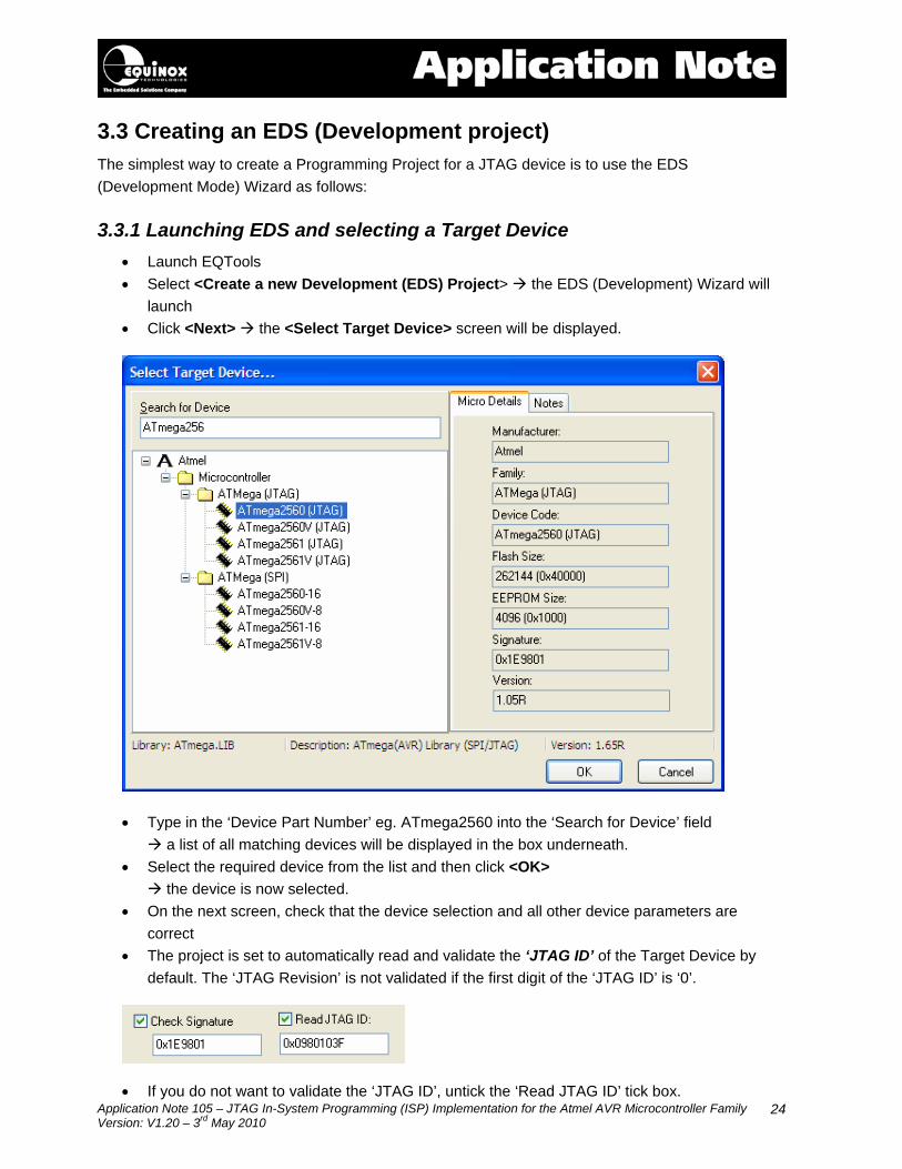
3.3 Creating an EDS (Development project) The simplest way to create a Programming Project for a JTAG device is to use the EDS (Development Mode) Wizard as follows: 3.3.1 Launching EDS and selecting a Target Device
• Launch EQTools • Select <Create a new Development (EDS) Project> the EDS (Development) Wizard will
launch • Click <Next> the <Select Target Device> screen will be displayed.
• Type in the ‘Device Part Number’ eg. ATmega2560 into the ‘Search for Device’ field a list of all matching devices will be displayed in the box underneath.
• Select the required device from the list and then click <OK> the device is now selected.
• On the next screen, check that the device selection and all other device parameters are correct
• The project is set to automatically read and validate the ‘JTAG ID’ of the Target Device by default. The ‘JTAG Revision’ is not validated if the first digit of the ‘JTAG ID’ is ‘0’.
• If you do not want to validate the ‘JTAG ID’, untick the ‘Read JTAG ID’ tick box.
Application Note 105 – JTAG In-System Programming (ISP) Implementation for the Atmel AVR Microcontroller Family Version: V1.20 – 3rd May 2010
25
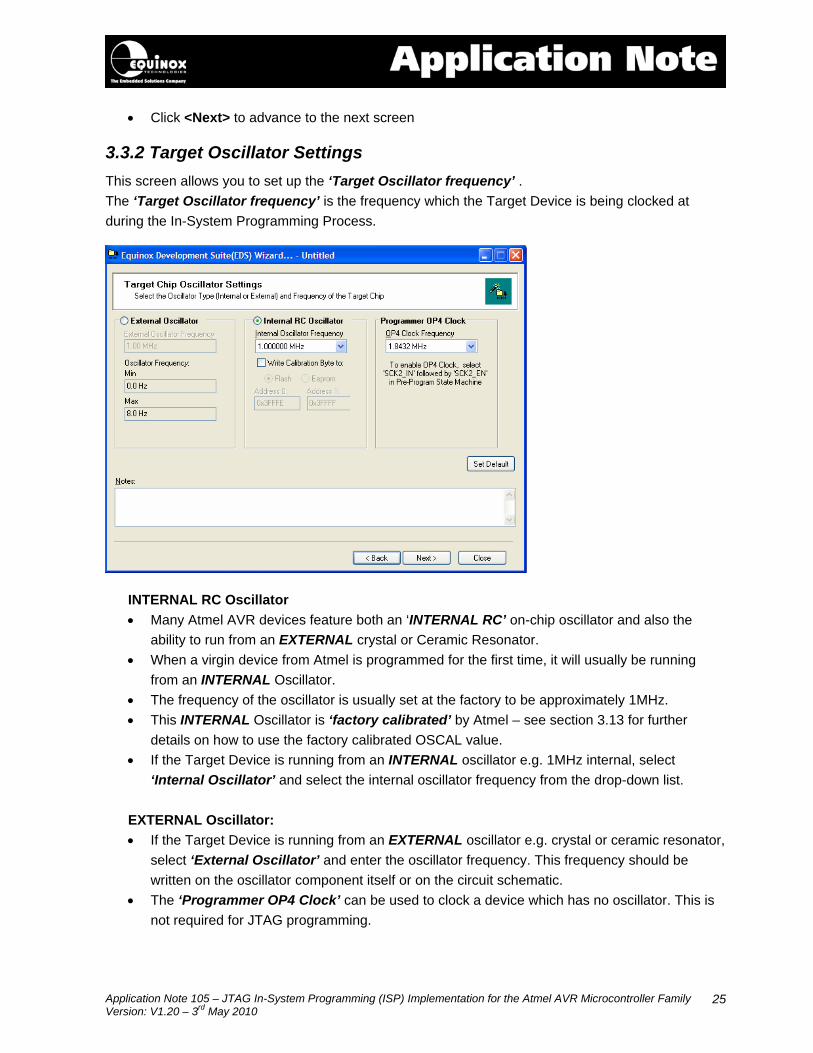
• Click <Next> to advance to the next screen 3.3.2 Target Oscillator Settings This screen allows you to set up the ‘Target Oscillator frequency’ . The ‘Target Oscillator frequency’ is the frequency which the Target Device is being clocked at during the In-System Programming Process.
INTERNAL RC Oscillator • Many Atmel AVR devices feature both an ‘INTERNAL RC’ on-chip oscillator and also the
ability to run from an EXTERNAL crystal or Ceramic Resonator. • When a virgin device from Atmel is programmed for the first time, it will usually be running
from an INTERNAL Oscillator. • The frequency of the oscillator is usually set at the factory to be approximately 1MHz. • This INTERNAL Oscillator is ‘factory calibrated’ by Atmel – see section 3.13 for further
details on how to use the factory calibrated OSCAL value. • If the Target Device is running from an INTERNAL oscillator e.g. 1MHz internal, select
‘Internal Oscillator’ and select the internal oscillator frequency from the drop-down list. EXTERNAL Oscillator: • If the Target Device is running from an EXTERNAL oscillator e.g. crystal or ceramic resonator,
select ‘External Oscillator’ and enter the oscillator frequency. This frequency should be written on the oscillator component itself or on the circuit schematic.
• The ‘Programmer OP4 Clock’ can be used to clock a device which has no oscillator. This is not required for JTAG programming.

Application Note 105 – JTAG In-System Programming (ISP) Implementation for the Atmel AVR Microcontroller Family Version: V1.20 – 3rd May 2010
26
Please note: The Target Oscillator speed is not technically required for JTAG programming as the programmer provides the clock during programming. If you do not know the Oscillator Frequency, simply leave all settings as the default values. 3.3.3 Target System – Power Supply Settings This screen allows you to set up the Power Supply characteristics of your Target System.
i. Select the Target Voltage
• This should be the voltage at which the Target System is being powered during the programming operation.
• Set the ‘Voltage Tolerance’ to be as wide as possible e.g. 500mV to allow for power supply variations. If the programmer is powering the Target System, this will also give a faster power-up time.
• It may be possible to power just the Target Microcontroller rather than the entire Target System.
ii. Set up the Target Powering and current parameters
• This option is only available for the PPM3-MK2 programmer. • If the programmer is to power the Target System, select <Programmer controlled Target
Power Supply: ON> • Set the ‘Maximum Current’ to the maximum possible current which the Target System could
draw from the programmer. • Leave all other settings as default.
Application Note 105 – JTAG In-System Programming (ISP) Implementation for the Atmel AVR Microcontroller Family Version: V1.20 – 3rd May 2010
27
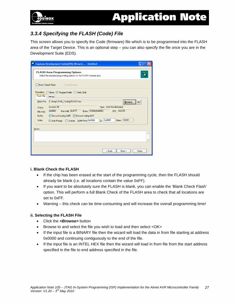
3.3.4 Specifying the FLASH (Code) File This screen allows you to specify the Code (firmware) file which is to be programmed into the FLASH area of the Target Device. This is an optional step – you can also specify the file once you are in the Development Suite (EDS).
i. Blank Check the FLASH
• If the chip has been erased at the start of the programming cycle, then the FLASH should already be blank (i.e. all locations contain the value 0xFF).
• If you want to be absolutely sure the FLASH is blank, you can enable the ‘Blank Check Flash’ option. This will perform a full Blank Check of the FLASH area to check that all locations are set to 0xFF.
• Warning – this check can be time-consuming and will increase the overall programming time! ii. Selecting the FLASH File
• Click the <Browse> button • Browse to and select the file you wish to load and then select <OK> • If the input file is a BINARY file then the wizard will load the data in from file starting at address
0x0000 and continuing contiguously to the end of the file. • If the input file is an INTEL HEX file then the wizard will load in from file from the start address
specified in the file to end address specified in the file.
Application Note 105 – JTAG In-System Programming (ISP) Implementation for the Atmel AVR Microcontroller Family Version: V1.20 – 3rd May 2010
28
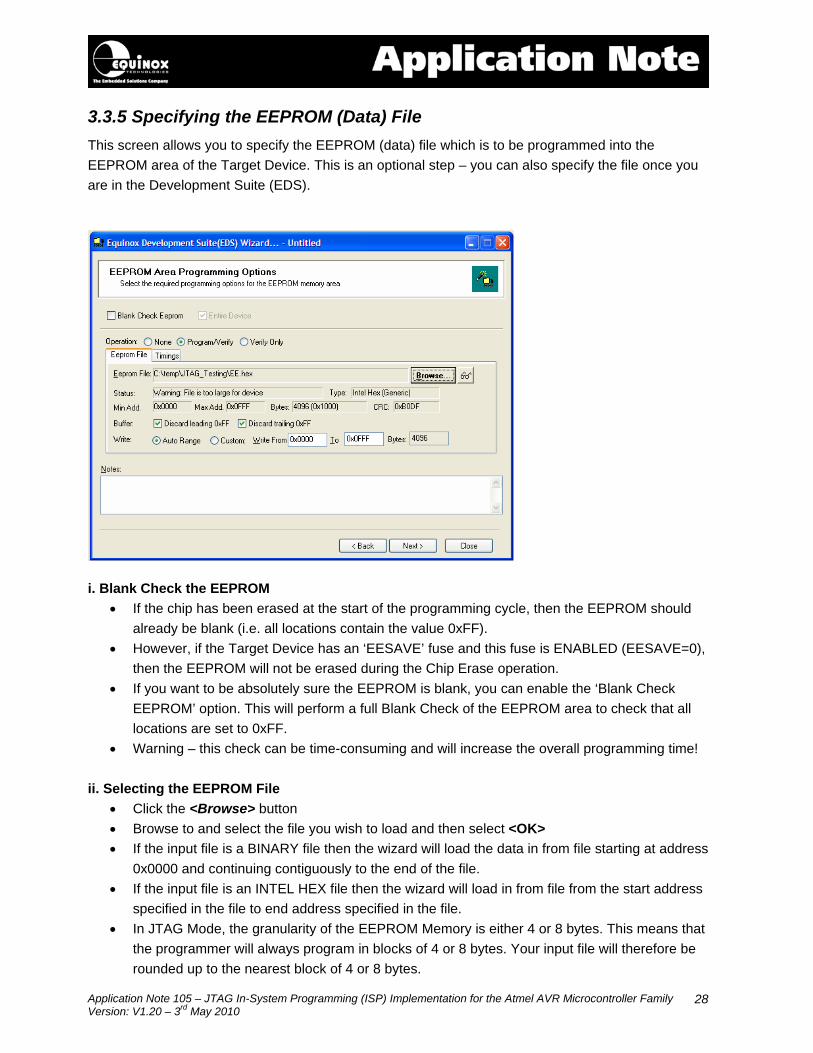
3.3.5 Specifying the EEPROM (Data) File This screen allows you to specify the EEPROM (data) file which is to be programmed into the EEPROM area of the Target Device. This is an optional step – you can also specify the file once you are in the Development Suite (EDS).
i. Blank Check the EEPROM
• If the chip has been erased at the start of the programming cycle, then the EEPROM should already be blank (i.e. all locations contain the value 0xFF).
• However, if the Target Device has an ‘EESAVE’ fuse and this fuse is ENABLED (EESAVE=0), then the EEPROM will not be erased during the Chip Erase operation.
• If you want to be absolutely sure the EEPROM is blank, you can enable the ‘Blank Check EEPROM’ option. This will perform a full Blank Check of the EEPROM area to check that all locations are set to 0xFF.
• Warning – this check can be time-consuming and will increase the overall programming time! ii. Selecting the EEPROM File
• Click the <Browse> button • Browse to and select the file you wish to load and then select <OK> • If the input file is a BINARY file then the wizard will load the data in from file starting at address
0x0000 and continuing contiguously to the end of the file. • If the input file is an INTEL HEX file then the wizard will load in from file from the start address
specified in the file to end address specified in the file. • In JTAG Mode, the granularity of the EEPROM Memory is either 4 or 8 bytes. This means that
the programmer will always program in blocks of 4 or 8 bytes. Your input file will therefore be rounded up to the nearest block of 4 or 8 bytes.
Application Note 105 – JTAG In-System Programming (ISP) Implementation for the Atmel AVR Microcontroller Family Version: V1.20 – 3rd May 2010
29
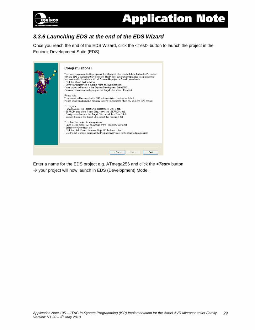
3.3.6 Launching EDS at the end of the EDS Wizard Once you reach the end of the EDS Wizard, click the <Test> button to launch the project in the Equinox Development Suite (EDS).
Enter a name for the EDS project e.g. ATmega256 and click the <Test> button
your project will now launch in EDS (Development) Mode.
Application Note 105 – JTAG In-System Programming (ISP) Implementation for the Atmel AVR Microcontroller Family Version: V1.20 – 3rd May 2010
30
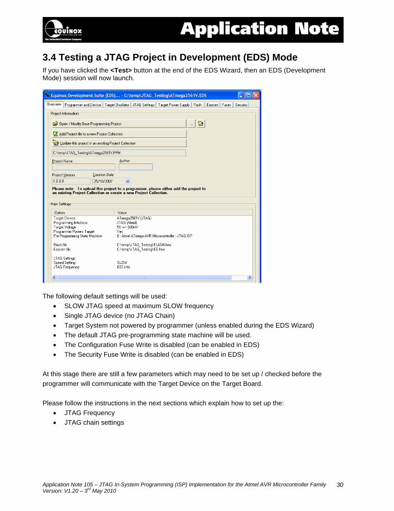
3.4 Testing a JTAG Project in Development (EDS) Mode If you have clicked the <Test> button at the end of the EDS Wizard, then an EDS (Development Mode) session will now launch.
The following default settings will be used:
• SLOW JTAG speed at maximum SLOW frequency • Single JTAG device (no JTAG Chain) • Target System not powered by programmer (unless enabled during the EDS Wizard) • The default JTAG pre-programming state machine will be used. • The Configuration Fuse Write is disabled (can be enabled in EDS) • The Security Fuse Write is disabled (can be enabled in EDS)
At this stage there are still a few parameters which may need to be set up / checked before the programmer will communicate with the Target Device on the Target Board. Please follow the instructions in the next sections which explain how to set up the:
• JTAG Frequency • JTAG chain settings
Application Note 105 – JTAG In-System Programming (ISP) Implementation for the Atmel AVR Microcontroller Family Version: V1.20 – 3rd May 2010
31
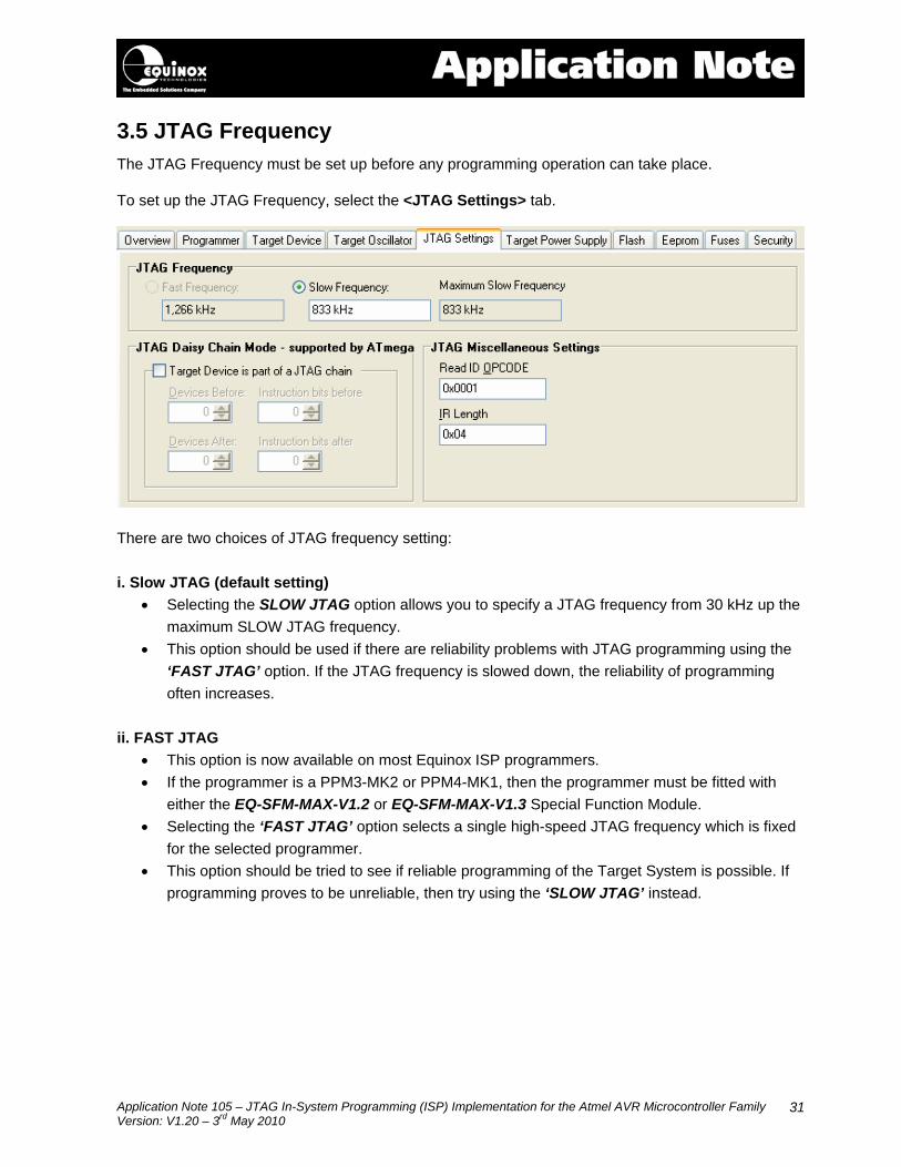
3.5 JTAG Frequency The JTAG Frequency must be set up before any programming operation can take place. To set up the JTAG Frequency, select the <JTAG Settings> tab.
There are two choices of JTAG frequency setting: i. Slow JTAG (default setting)
• Selecting the SLOW JTAG option allows you to specify a JTAG frequency from 30 kHz up the maximum SLOW JTAG frequency.
• This option should be used if there are reliability problems with JTAG programming using the ‘FAST JTAG’ option. If the JTAG frequency is slowed down, the reliability of programming often increases.
ii. FAST JTAG
• This option is now available on most Equinox ISP programmers. • If the programmer is a PPM3-MK2 or PPM4-MK1, then the programmer must be fitted with
either the EQ-SFM-MAX-V1.2 or EQ-SFM-MAX-V1.3 Special Function Module. • Selecting the ‘FAST JTAG’ option selects a single high-speed JTAG frequency which is fixed
for the selected programmer. • This option should be tried to see if reliable programming of the Target System is possible. If
programming proves to be unreliable, then try using the ‘SLOW JTAG’ instead.
Application Note 105 – JTAG In-System Programming (ISP) Implementation for the Atmel AVR Microcontroller Family Version: V1.20 – 3rd May 2010
32
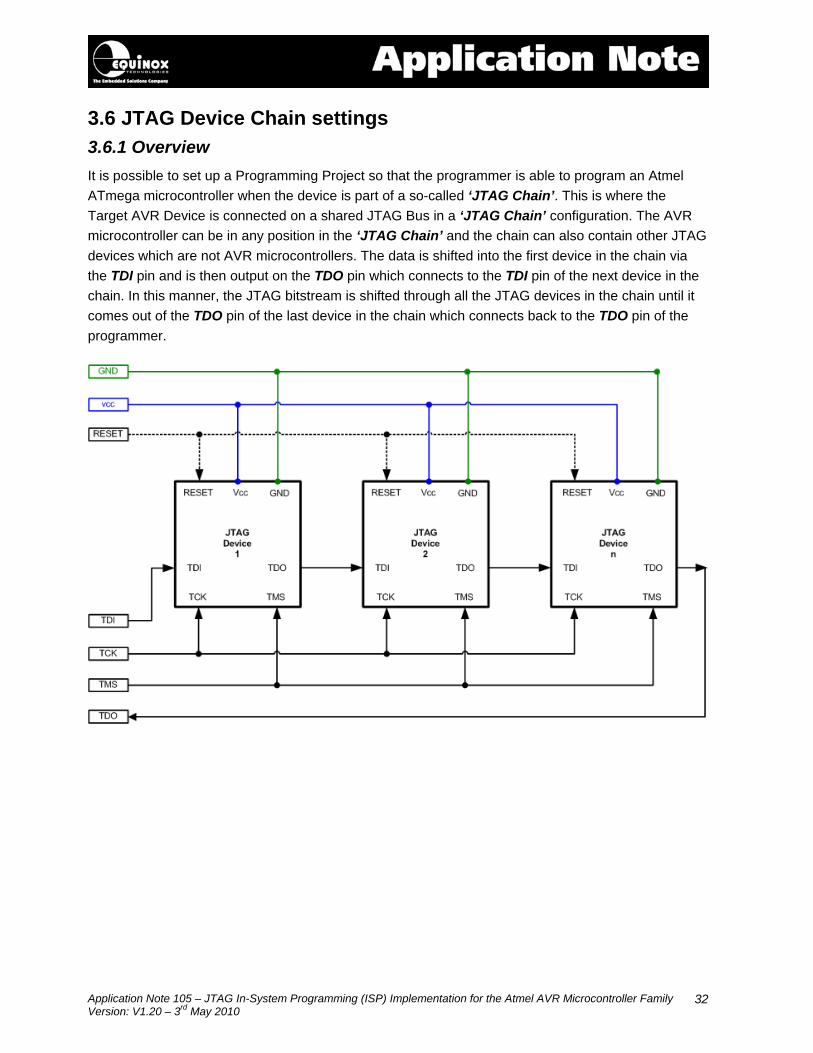
3.6 JTAG Device Chain settings 3.6.1 Overview It is possible to set up a Programming Project so that the programmer is able to program an Atmel ATmega microcontroller when the device is part of a so-called ‘JTAG Chain’. This is where the Target AVR Device is connected on a shared JTAG Bus in a ‘JTAG Chain’ configuration. The AVR microcontroller can be in any position in the ‘JTAG Chain’ and the chain can also contain other JTAG devices which are not AVR microcontrollers. The data is shifted into the first device in the chain via the TDI pin and is then output on the TDO pin which connects to the TDI pin of the next device in the chain. In this manner, the JTAG bitstream is shifted through all the JTAG devices in the chain until it comes out of the TDO pin of the last device in the chain which connects back to the TDO pin of the programmer.
Application Note 105 – JTAG In-System Programming (ISP) Implementation for the Atmel AVR Microcontroller Family Version: V1.20 – 3rd May 2010
33
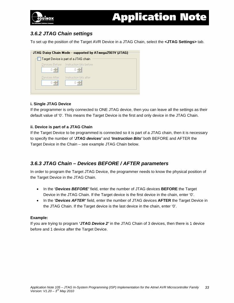
3.6.2 JTAG Chain settings To set up the position of the Target AVR Device in a JTAG Chain, select the <JTAG Settings> tab.
i. Single JTAG Device If the programmer is only connected to ONE JTAG device, then you can leave all the settings as their default value of ‘0’. This means the Target Device is the first and only device in the JTAG Chain. ii. Device is part of a JTAG Chain If the Target Device to be programmed is connected so it is part of a JTAG chain, then it is necessary to specify the number of ‘JTAG devices’ and ‘Instruction Bits’ both BEFORE and AFTER the Target Device in the Chain – see example JTAG Chain below. 3.6.3 JTAG Chain – Devices BEFORE / AFTER parameters In order to program the Target JTAG Device, the programmer needs to know the physical position of the Target Device in the JTAG Chain.
• In the ‘Devices BEFORE’ field, enter the number of JTAG devices BEFORE the Target Device in the JTAG Chain. If the Target device is the first device in the chain, enter ‘0’.
• In the ‘Devices AFTER’ field, enter the number of JTAG devices AFTER the Target Device in the JTAG Chain. If the Target device is the last device in the chain, enter ‘0’.
Example: If you are trying to program ‘JTAG Device 2’ in the JTAG Chain of 3 devices, then there is 1 device before and 1 device after the Target Device.
Application Note 105 – JTAG In-System Programming (ISP) Implementation for the Atmel AVR Microcontroller Family Version: V1.20 – 3rd May 2010
34
3.6.4 JTAG Chain – Instruction Bits BEFORE / AFTER parameters In order to program the Target Device, the programmer needs to know the total number of JTAG ‘Instruction Register’ bits contained in the JTAG devices BEFORE and AFTER the Target Device. The programmer then pads all outgoing bit streams with the relevant numbers of dummy bits so only the Target Device is actually accessed / programmed.
• You can find the ‘JTAG Instruction Register’ width (number of bits) in the manufacturer’s datasheet for each JTAG device you are looking to program in the chain.
• All Atmel ATmega AVR microcontrollers have a ‘JTAG Instruction Register’ width of 4 bits. • All Atmel ATFxxxx CPLD’s have an instruction width of 8 bits.
3.6.5 Calculating the ‘Bits Before’ value To calculate the ‘Bits Before’ value:
• Find out the ‘JTAG Instruction Register’ width (number of bits) in the manufacturers datasheet for each JTAG device you are looking to program in the chain.
• Add together all the ‘JTAG Instruction Register’ widths for JTAG devices BEFORE the Target Device
• Enter this value in the ‘Bits BEFORE’ field Example:
• In our example JTAG Chain with 3 AVR devices, each AVR device will have a ‘JTAG Instruction Register’ width of 4 bits.
• If you are trying to program ‘JTAG Device 2’ in the JTAG Chain of 3 devices, then there is 1 AVR device before Device 2 so the ‘Bits BEFORE’ field should be set to 4.
3.6.6 Calculating the ‘Bits After’ value To calculate the ‘Bits After’ value:
• Find out the ‘JTAG Instruction Register’ width (number of bits) in the manufacturers datasheet for each JTAG device you are looking to program in the chain.
• Add together all the ‘JTAG Instruction Register’ widths for JTAG devices AFTER the Target Device
• Enter this value in the ‘Bits AFTER’ field Example:
• In our example JTAG Chain with 3 AVR devices, each AVR device will have a ‘JTAG Instruction Register’ width of 4 bits.
• If you are trying to program ‘JTAG Device 2’ in the JTAG Chain of 3 devices, then there is 1 AVR device after Device 2 so the ‘Bits After’ field should be set to 4.
Application Note 105 – JTAG In-System Programming (ISP) Implementation for the Atmel AVR Microcontroller Family Version: V1.20 – 3rd May 2010
35
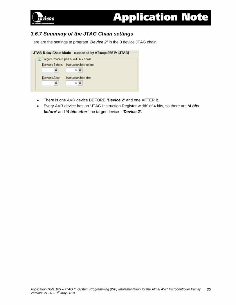
3.6.7 Summary of the JTAG Chain settings Here are the settings to program ’Device 2’ in the 3 device JTAG chain:
• There is one AVR device BEFORE ‘Device 2’ and one AFTER it. • Every AVR device has an ‘JTAG Instruction Register width’ of 4 bits, so there are ‘4 bits
before’ and ‘4 bits after’ the target device - ‘Device 2’.
Application Note 105 – JTAG In-System Programming (ISP) Implementation for the Atmel AVR Microcontroller Family Version: V1.20 – 3rd May 2010
36
3.7 Testing JTAG communication with the Target Chip To make sure that the programmer can communicate to the Target JTAG device, try reading back the Device Signature as follows:
• Select the <FLASH> tab • Locate the <Check Sig> button on the right-hand side of the screen and click it.
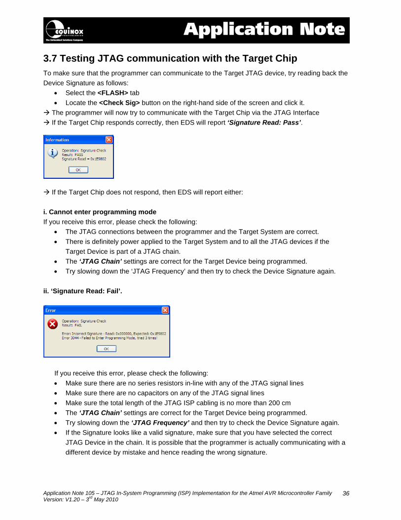
The programmer will now try to communicate with the Target Chip via the JTAG Interface If the Target Chip responds correctly, then EDS will report ‘Signature Read: Pass’.
If the Target Chip does not respond, then EDS will report either: i. Cannot enter programming mode If you receive this error, please check the following:
• The JTAG connections between the programmer and the Target System are correct. • There is definitely power applied to the Target System and to all the JTAG devices if the
Target Device is part of a JTAG chain. • The ‘JTAG Chain’ settings are correct for the Target Device being programmed. • Try slowing down the ‘JTAG Frequency’ and then try to check the Device Signature again.
ii. ‘Signature Read: Fail’.
If you receive this error, please check the following: • Make sure there are no series resistors in-line with any of the JTAG signal lines • Make sure there are no capacitors on any of the JTAG signal lines • Make sure the total length of the JTAG ISP cabling is no more than 200 cm • The ‘JTAG Chain’ settings are correct for the Target Device being programmed. • Try slowing down the ‘JTAG Frequency’ and then try to check the Device Signature again. • If the Signature looks like a valid signature, make sure that you have selected the correct
JTAG Device in the chain. It is possible that the programmer is actually communicating with a different device by mistake and hence reading the wrong signature.
Application Note 105 – JTAG In-System Programming (ISP) Implementation for the Atmel AVR Microcontroller Family Version: V1.20 – 3rd May 2010
37
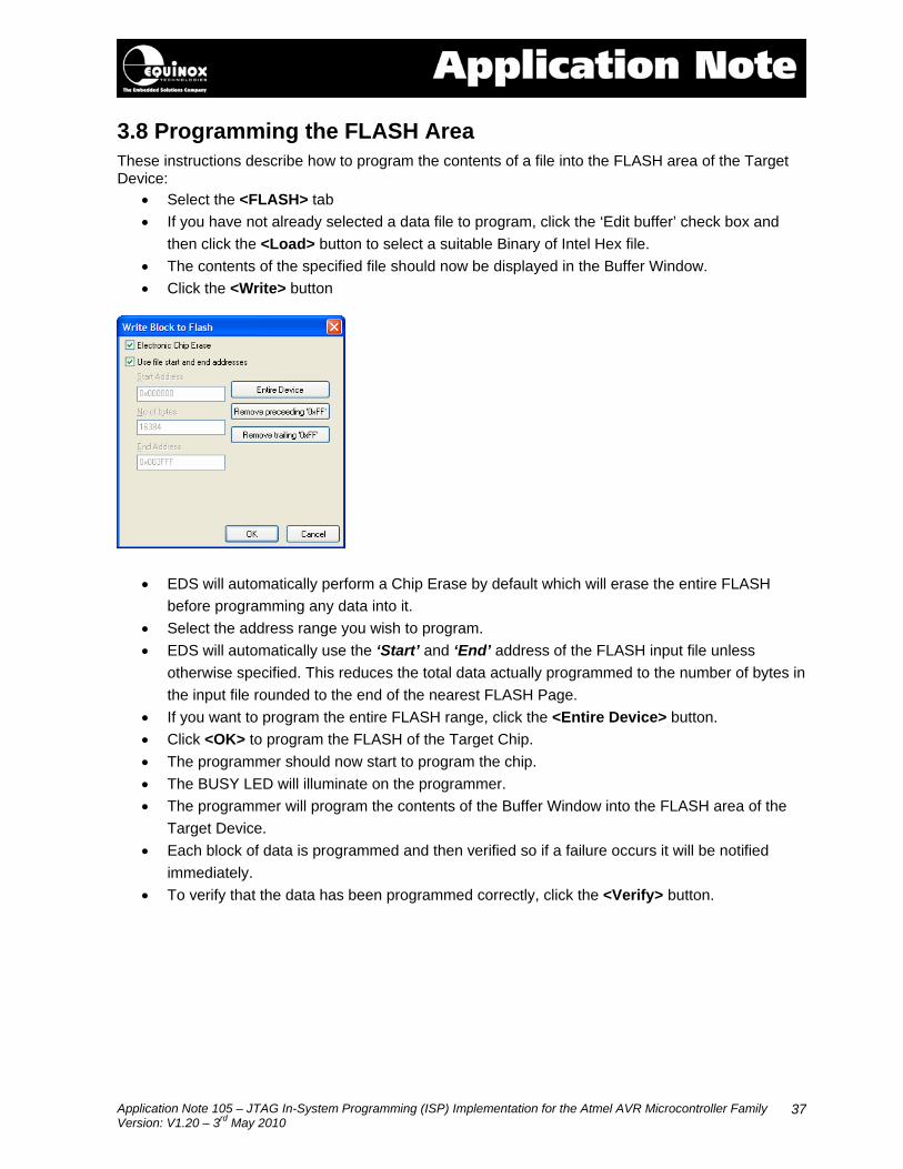
3.8 Programming the FLASH Area These instructions describe how to program the contents of a file into the FLASH area of the Target Device:
• Select the <FLASH> tab • If you have not already selected a data file to program, click the ‘Edit buffer’ check box and
then click the <Load> button to select a suitable Binary of Intel Hex file. • The contents of the specified file should now be displayed in the Buffer Window. • Click the <Write> button
• EDS will automatically perform a Chip Erase by default which will erase the entire FLASH
before programming any data into it. • Select the address range you wish to program. • EDS will automatically use the ‘Start’ and ‘End’ address of the FLASH input file unless
otherwise specified. This reduces the total data actually programmed to the number of bytes in the input file rounded to the end of the nearest FLASH Page.
• If you want to program the entire FLASH range, click the <Entire Device> button. • Click <OK> to program the FLASH of the Target Chip. • The programmer should now start to program the chip. • The BUSY LED will illuminate on the programmer. • The programmer will program the contents of the Buffer Window into the FLASH area of the
Target Device. • Each block of data is programmed and then verified so if a failure occurs it will be notified
immediately. • To verify that the data has been programmed correctly, click the <Verify> button.
Application Note 105 – JTAG In-System Programming (ISP) Implementation for the Atmel AVR Microcontroller Family Version: V1.20 – 3rd May 2010
38
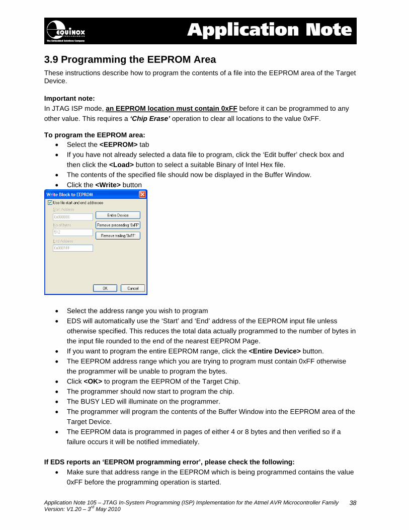
3.9 Programming the EEPROM Area These instructions describe how to program the contents of a file into the EEPROM area of the Target Device. Important note: In JTAG ISP mode, an EEPROM location must contain 0xFF before it can be programmed to any other value. This requires a ‘Chip Erase’ operation to clear all locations to the value 0xFF. To program the EEPROM area:
• Select the <EEPROM> tab • If you have not already selected a data file to program, click the ‘Edit buffer’ check box and
then click the <Load> button to select a suitable Binary of Intel Hex file. • The contents of the specified file should now be displayed in the Buffer Window. • Click the <Write> button
• Select the address range you wish to program • EDS will automatically use the ‘Start’ and ‘End’ address of the EEPROM input file unless
otherwise specified. This reduces the total data actually programmed to the number of bytes in the input file rounded to the end of the nearest EEPROM Page.
• If you want to program the entire EEPROM range, click the <Entire Device> button. • The EEPROM address range which you are trying to program must contain 0xFF otherwise
the programmer will be unable to program the bytes. • Click <OK> to program the EEPROM of the Target Chip. • The programmer should now start to program the chip. • The BUSY LED will illuminate on the programmer. • The programmer will program the contents of the Buffer Window into the EEPROM area of the
Target Device. • The EEPROM data is programmed in pages of either 4 or 8 bytes and then verified so if a
failure occurs it will be notified immediately. If EDS reports an ‘EEPROM programming error’, please check the following:
• Make sure that address range in the EEPROM which is being programmed contains the value 0xFF before the programming operation is started.

Application Note 105 – JTAG In-System Programming (ISP) Implementation for the Atmel AVR Microcontroller Family Version: V1.20 – 3rd May 2010
39
• This may require a Chip Erase operation to be performed because in JTAG Mode an EEPROM Page does NOT get automatically erased during a program operation.
• To Erase the EEPROM area to value 0xFF, you may need to set the ‘EESAVE’ fuse to a ‘1’ and then perform a Chip Erase operation.
3.10 Erasing the FLASH / EEPROM area It is possible to erase the FLASH and / or EEPROM area of a Target Device by clicking the <Erase> button. This will also erase the Security Lock Bits changing all the Lock Bit values from ‘0’ to ‘1’. The Configuration Fuses are not affected by a Chip Erase operation. 3.10.1 Erasing the FLASH area The only way to erase the FLASH area of the Target Device is to use the ‘Chip Erase’ command:
• Select the <FLASH> tab • Click the <Erase> button • This will send the ‘Chip Erase’ command to the Target Device. • The Target Device will then erase the FLASH (and EEPROM as long as the EESAVE flag is
not set to 0) • To confirm that the FLASH / EEPROM is definitely blank, you can choose to perform a Blank
Check operation. 3.10.2 Erasing the EEPROM area – special considerations The only way to erase the EEPROM area of the Target Device is to use the ‘Chip Erase’ command:
• Select the <EEPROM> tab • Click the <Erase> button • This will send the ‘Chip Erase’ command to the Target Device. • The Target Device will then automatically erase the FLASH followed by the EEPROM areas. • The EEPROM area will only be erased if the EESAVE flag is set to ‘1’. • To confirm that the FLASH / EEPROM is definitely blank, you can choose to perform a Blank
Check operation. • If the EEPROM is still not blank after the Erase Operation, check that the EESAVE fuse is
definitely set to ‘1’. Important note: In JTAG ISP mode only, it is not possible for the programmer to write any bit of EEPROM from a ‘1’ to a ‘0’. This means that each EEPROM location must contain 0xFF before it can be programmed to any other value. This requires a Chip Erase operation to clear all locations to the value 0xFF.
Application Note 105 – JTAG In-System Programming (ISP) Implementation for the Atmel AVR Microcontroller Family Version: V1.20 – 3rd May 2010
40
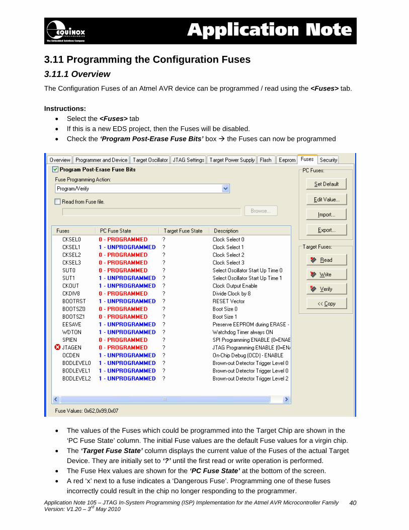
3.11 Programming the Configuration Fuses 3.11.1 Overview The Configuration Fuses of an Atmel AVR device can be programmed / read using the <Fuses> tab. Instructions:
• Select the <Fuses> tab • If this is a new EDS project, then the Fuses will be disabled. • Check the ‘Program Post-Erase Fuse Bits’ box the Fuses can now be programmed
• The values of the Fuses which could be programmed into the Target Chip are shown in the ‘PC Fuse State’ column. The initial Fuse values are the default Fuse values for a virgin chip.
• The ‘Target Fuse State’ column displays the current value of the Fuses of the actual Target Device. They are initially set to ‘?’ until the first read or write operation is performed.
• The Fuse Hex values are shown for the ‘PC Fuse State’ at the bottom of the screen. • A red ‘x’ next to a fuse indicates a ‘Dangerous Fuse’. Programming one of these fuses
incorrectly could result in the chip no longer responding to the programmer.
Application Note 105 – JTAG In-System Programming (ISP) Implementation for the Atmel AVR Microcontroller Family Version: V1.20 – 3rd May 2010
41
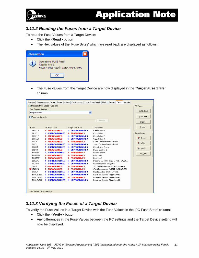
3.11.2 Reading the Fuses from a Target Device To read the Fuse Values from a Target Device:
• Click the <Read> button • The Hex values of the ‘Fuse Bytes’ which are read back are displayed as follows:
• The Fuse values from the Target Device are now displayed in the ‘Target Fuse State’ column.
3.11.3 Verifying the Fuses of a Target Device To verify the Fuse Values in a Target Device with the Fuse Values in the ‘PC Fuse State’ column:
• Click the <Verify> button • Any differences in the Fuse Values between the PC settings and the Target Device setting will
now be displayed.
Application Note 105 – JTAG In-System Programming (ISP) Implementation for the Atmel AVR Microcontroller Family Version: V1.20 – 3rd May 2010
42
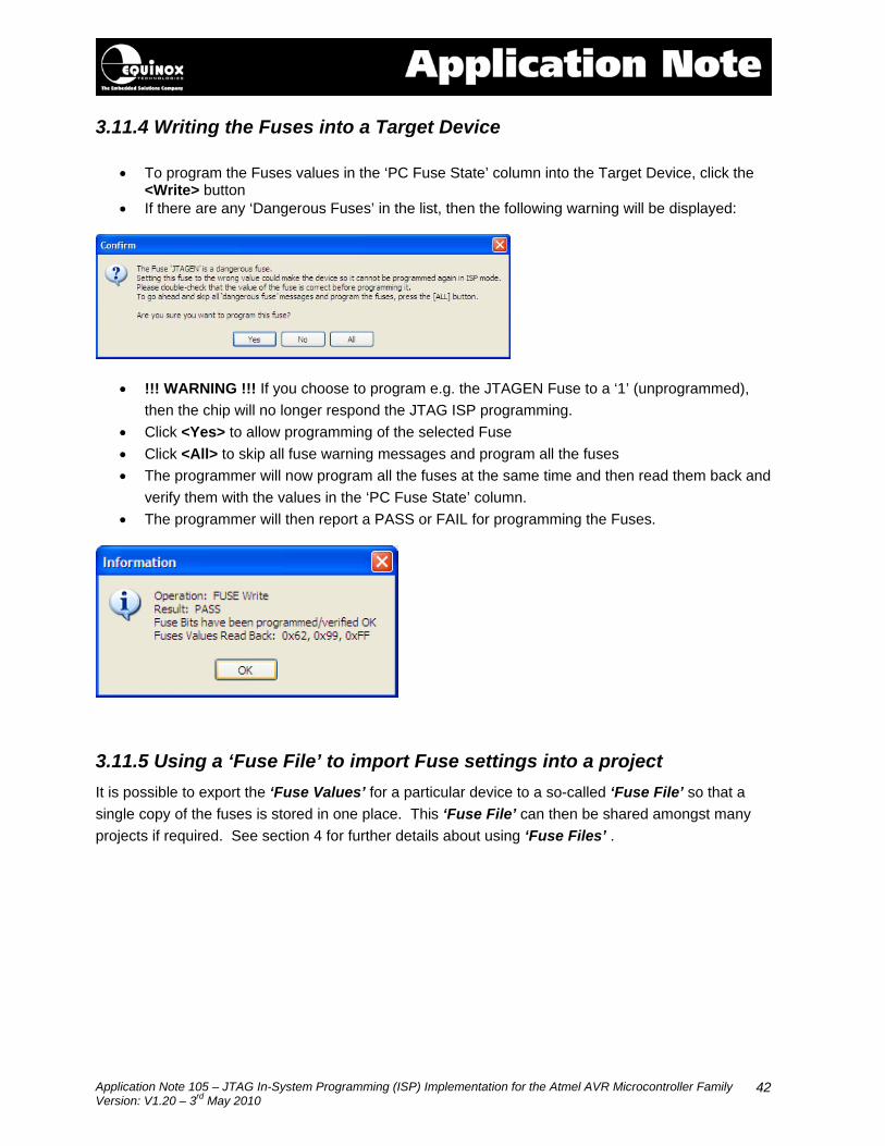
3.11.4 Writing the Fuses into a Target Device
• To program the Fuses values in the ‘PC Fuse State’ column into the Target Device, click the <Write> button
• If there are any ‘Dangerous Fuses’ in the list, then the following warning will be displayed:
• !!! WARNING !!! If you choose to program e.g. the JTAGEN Fuse to a ‘1’ (unprogrammed), then the chip will no longer respond the JTAG ISP programming.
• Click <Yes> to allow programming of the selected Fuse • Click <All> to skip all fuse warning messages and program all the fuses • The programmer will now program all the fuses at the same time and then read them back and
verify them with the values in the ‘PC Fuse State’ column. • The programmer will then report a PASS or FAIL for programming the Fuses.
3.11.5 Using a ‘Fuse File’ to import Fuse settings into a project It is possible to export the ‘Fuse Values’ for a particular device to a so-called ‘Fuse File’ so that a single copy of the fuses is stored in one place. This ‘Fuse File’ can then be shared amongst many projects if required. See section 4 for further details about using ‘Fuse Files’ .
Application Note 105 – JTAG In-System Programming (ISP) Implementation for the Atmel AVR Microcontroller Family Version: V1.20 – 3rd May 2010
43
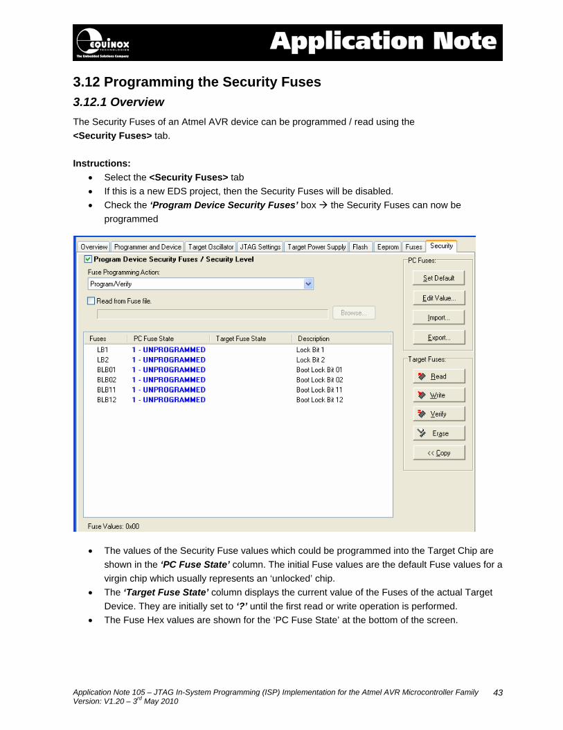
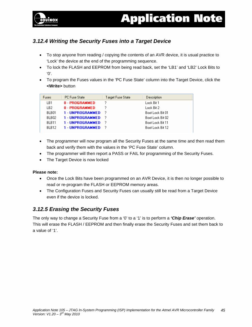
3.12 Programming the Security Fuses 3.12.1 Overview The Security Fuses of an Atmel AVR device can be programmed / read using the <Security Fuses> tab. Instructions:
• Select the <Security Fuses> tab • If this is a new EDS project, then the Security Fuses will be disabled. • Check the ‘Program Device Security Fuses’ box the Security Fuses can now be
programmed
• The values of the Security Fuse values which could be programmed into the Target Chip are shown in the ‘PC Fuse State’ column. The initial Fuse values are the default Fuse values for a virgin chip which usually represents an ‘unlocked’ chip.
• The ‘Target Fuse State’ column displays the current value of the Fuses of the actual Target Device. They are initially set to ‘?’ until the first read or write operation is performed.
• The Fuse Hex values are shown for the ‘PC Fuse State’ at the bottom of the screen.
Application Note 105 – JTAG In-System Programming (ISP) Implementation for the Atmel AVR Microcontroller Family Version: V1.20 – 3rd May 2010
44
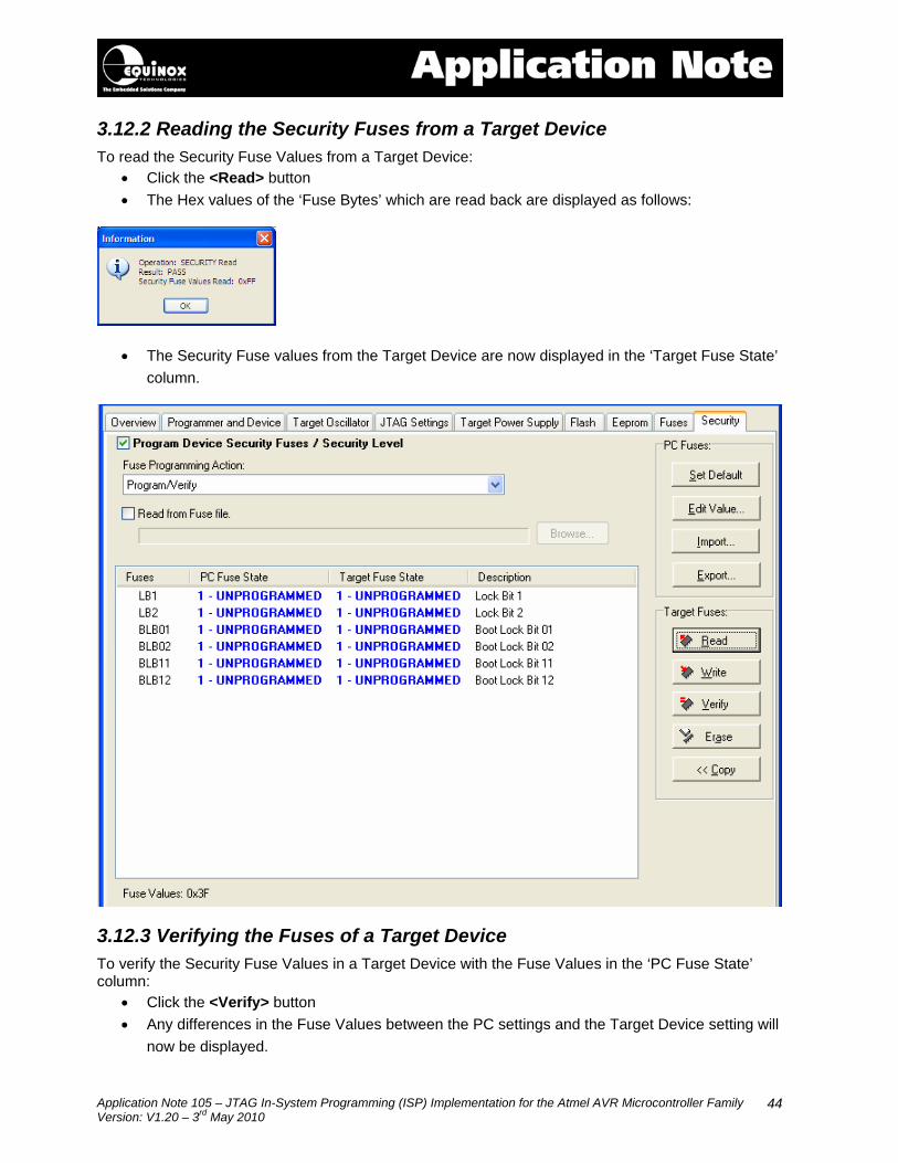
3.12.2 Reading the Security Fuses from a Target Device To read the Security Fuse Values from a Target Device:
• Click the <Read> button • The Hex values of the ‘Fuse Bytes’ which are read back are displayed as follows:
• The Security Fuse values from the Target Device are now displayed in the ‘Target Fuse State’ column.
3.12.3 Verifying the Fuses of a Target Device To verify the Security Fuse Values in a Target Device with the Fuse Values in the ‘PC Fuse State’ column:
• Click the <Verify> button • Any differences in the Fuse Values between the PC settings and the Target Device setting will
now be displayed.
Application Note 105 – JTAG In-System Programming (ISP) Implementation for the Atmel AVR Microcontroller Family Version: V1.20 – 3rd May 2010
45
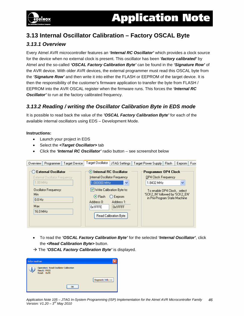
3.12.4 Writing the Security Fuses into a Target Device
• To stop anyone from reading / copying the contents of an AVR device, it is usual practice to ‘Lock’ the device at the end of the programming sequence.
• To lock the FLASH and EEPROM from being read back, set the ‘LB1’ and ‘LB2’ Lock Bits to ‘0’.
• To program the Fuses values in the ‘PC Fuse State’ column into the Target Device, click the <Write> button
• The programmer will now program all the Security Fuses at the same time and then read them
back and verify them with the values in the ‘PC Fuse State’ column. • The programmer will then report a PASS or FAIL for programming of the Security Fuses. • The Target Device is now locked
Please note:
• Once the Lock Bits have been programmed on an AVR Device, it is then no longer possible to read or re-program the FLASH or EEPROM memory areas.
• The Configuration Fuses and Security Fuses can usually still be read from a Target Device even if the device is locked.
3.12.5 Erasing the Security Fuses The only way to change a Security Fuse from a ‘0’ to a ‘1’ is to perform a ‘Chip Erase’ operation. This will erase the FLASH / EEPROM and then finally erase the Security Fuses and set them back to a value of ‘1’.
Application Note 105 – JTAG In-System Programming (ISP) Implementation for the Atmel AVR Microcontroller Family Version: V1.20 – 3rd May 2010
46
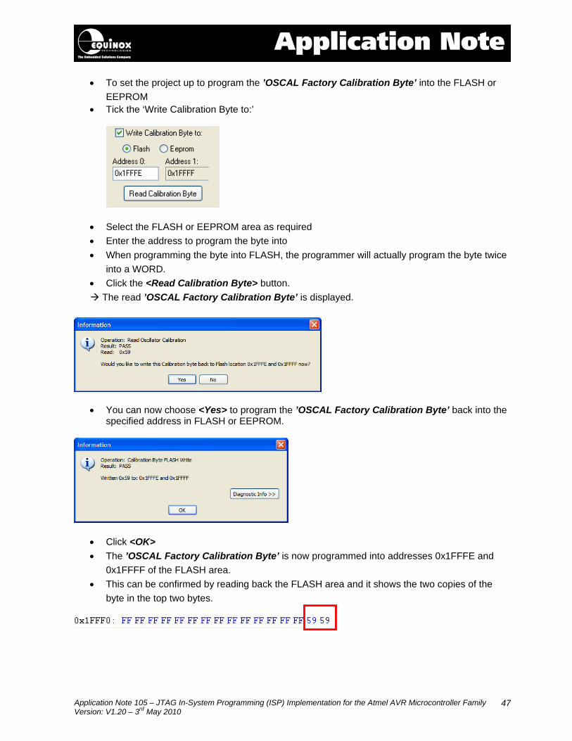
3.13 Internal Oscillator Calibration – Factory OSCAL Byte 3.13.1 Overview Every Atmel AVR microcontroller features an ‘Internal RC Oscillator’ which provides a clock source for the device when no external clock is present. This oscillator has been ‘factory calibrated’ by Atmel and the so-called ‘OSCAL Factory Calibration Byte’ can be found in the ‘Signature Row’ of the AVR device. With older AVR devices, the external programmer must read this OSCAL byte from the ‘Signature Row’ and then write it into either the FLASH or EEPROM of the target device. It is then the responsibility of the customer’s firmware application to transfer the byte from FLASH / EEPROM into the AVR OSCAL register when the firmware runs. This forces the ‘Internal RC Oscillator’ to run at the factory calibrated frequency. 3.13.2 Reading / writing the Oscillator Calibration Byte in EDS mode It is possible to read back the value of the ’OSCAL Factory Calibration Byte’ for each of the available internal oscillators using EDS – Development Mode. Instructions:
• Launch your project in EDS • Select the <Target Oscillator> tab • Click the ‘Internal RC Oscillator’ radio button – see screenshot below
• To read the ’OSCAL Factory Calibration Byte’ for the selected ‘Internal Oscillator’, click the <Read Calibration Byte> button.
The ’OSCAL Factory Calibration Byte’ is displayed.
Application Note 105 – JTAG In-System Programming (ISP) Implementation for the Atmel AVR Microcontroller Family Version: V1.20 – 3rd May 2010
47
• To set the project up to program the ’OSCAL Factory Calibration Byte’ into the FLASH or EEPROM
• Tick the ‘Write Calibration Byte to:’
• Select the FLASH or EEPROM area as required • Enter the address to program the byte into • When programming the byte into FLASH, the programmer will actually program the byte twice
into a WORD. • Click the <Read Calibration Byte> button.
The read ’OSCAL Factory Calibration Byte’ is displayed.
• You can now choose <Yes> to program the ’OSCAL Factory Calibration Byte’ back into the specified address in FLASH or EEPROM.
• Click <OK> • The ’OSCAL Factory Calibration Byte’ is now programmed into addresses 0x1FFFE and
0x1FFFF of the FLASH area. • This can be confirmed by reading back the FLASH area and it shows the two copies of the
byte in the top two bytes.

Application Note 105 – JTAG In-System Programming (ISP) Implementation for the Atmel AVR Microcontroller Family Version: V1.20 – 3rd May 2010
48
3.13.3 Writing the Oscillator Calibration Byte in STANDALONE mode It is possible to get the programmer to automatically read the ’OSCAL Factory Calibration Byte’ and program it into a specified location in FLASH or EEPROM using a Standalone Project. This is ideal for production environments where the programmer is used without a PC. Instructions:
• Follow the instructions in the previous section to set up the address into which the ’OSCAL Factory Calibration Byte’ is to be programmed.
• Make sure that your FLASH or EEPROM data files to not also write data to the same location where the ’OSCAL Factory Calibration Byte’ is to be programmed
• Compile the project and upload it to the programmer. • When the project is executed, it will perform the other actions specified in the project and then
automatically read the ’OSCAL Factory Calibration Byte’ and write it into the specified address in FLASH or EEPROM.
3.14 Exporting an EDS Project to a Standalone Project Once you have fully tested your EDS Development Project, it is possible to add the project to a Project Collection and then upload it to a programmer as a so-called ‘Standalone Project’. The project can then be executed on a programmer without requiring any form of PC control. Please follow the instructions detailed in Section 6 to upload your EDS project to a programmer.

Application Note 105 – JTAG In-System Programming (ISP) Implementation for the Atmel AVR Microcontroller Family Version: V1.20 – 3rd May 2010
49
4.0 Exporting / Importing Fuse Settings to / from File 4.1 Overview One of the new power features of EQTools is the ability to export the ‘Fuse Settings’ for a Programming Project to a Fuse File (*.eff). This allows the settings for all the fuses to be contained in one Fuse File which can then be imported into any of the Fuse tabs in Project Manager or in the <Fuses> tab in EDS. In this way, the values of all the Fuses for a particular project can be shared with other projects. This helps to ensure that the correct fuse values are specified in all projects. 4.2 Exporting the Fuse Settings to a Fuse File To export the settings of the ‘Local Fuses’ column to a fuse File:
• Select the EDS <Fuses> Tab • Set up the ‘Local Fuses’ to the correct values for your Target Device. • Click the <Export> button a file browser is displayed. • Enter a suitable name for your Fuse File eg. project_fuses.eff • Click <Save> The ‘Local Fuses’ column is transferred to your specified Fuse File (*.eff).
4.3 Copying the Fuses from a Target Device To copy the Fuses from the Target Device to a Fuse File:
• Select the EDS <Fuses> Tab • Click the <Read> button
the Fuses are read from the Target Device and are then displayed in the ‘Target State’ column.
• Click the <<Copy button the Fuse settings read from the Target Device are copied into the ‘Local State’ fuse
column. • Click the <Export> button a file browser is displayed. • Enter a suitable name for your Fuse File eg. project_fuses.eff • Click <Save> The ‘Local Fuses’ column is transferred to your specified Fuse File (*.eff).
4.4 Importing the Fuse Settings from a Fuse File To import the settings of the ‘Local Fuses’ column from a Fuse File:
• Select the EDS <Fuses> Tab • Click the <Import> button a file browser appears • Browse to and select your Fuse File (*.eff)
The Fuse settings are then automatically copied from the Fuse File to the ‘Local Fuses’ column.
• To program these settings into a Target Device, click <Write>.

Application Note 105 – JTAG In-System Programming (ISP) Implementation for the Atmel AVR Microcontroller Family Version: V1.20 – 3rd May 2010
50

Application Note 105 – JTAG In-System Programming (ISP) Implementation for the Atmel AVR Microcontroller Family Version: V1.20 – 3rd May 2010
51
5.0 Importing Fuse Settings in HEX format from AVR Studio 5.1 Overview If the original firmware for your project has been developed using the Atmel ‘AVR Studio’ software, then it is likely that both the AVR ‘Configuration Fuse settings’ and the ‘Security Fuse Settings’ are defined as so-called ‘Hex Fuse Bytes’. This is the raw version of the fuses where each ‘Hex Fuse Byte’ can represent up to 8 individual ‘Boolean Fuses’. It is possible to import the ‘Hex Fuse Bytes’ from AVR Studio into an EQTools project by following the instructions in the next section. 5.2 Finding the AVR Studio ‘Hex Fuse Values’ In the Atmel ‘AVR Studio’ software, the ‘Configuration Fuse settings’ for your project are displayed on the <Fuses> tab – see screenshot below.
The ‘AVR Studio’ software displays a high-level overview of the fuses, grouping similar fuses together with more meaningful group names eg. ‘BODELEVEL’ is made up of two fuses: BODLEVEL0 and BODLEV1 and the fuse ‘SUT_CKSEL’ actually represents the following six Boolean fuses: SUT0, SUT1, CKSEL0, CKSEL1, CKSEL2, CKSEL3.
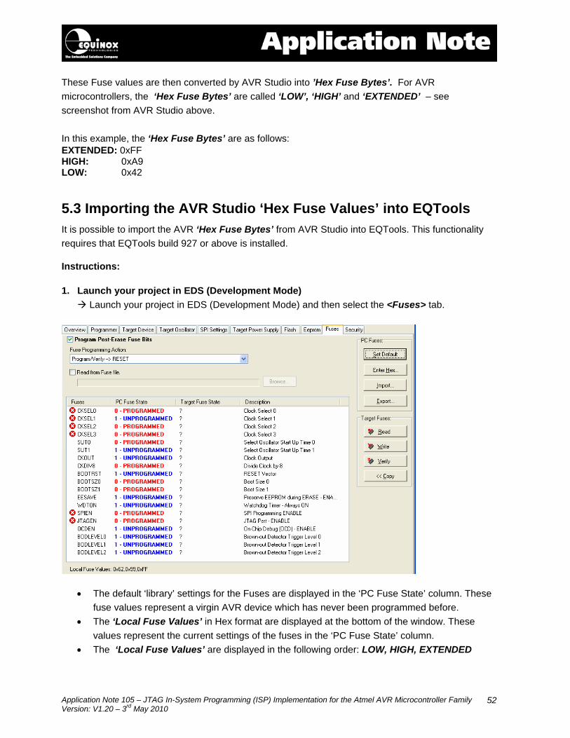
Application Note 105 – JTAG In-System Programming (ISP) Implementation for the Atmel AVR Microcontroller Family Version: V1.20 – 3rd May 2010
52
These Fuse values are then converted by AVR Studio into ’Hex Fuse Bytes’. For AVR microcontrollers, the ‘Hex Fuse Bytes’ are called ‘LOW’, ‘HIGH’ and ‘EXTENDED’ – see screenshot from AVR Studio above. In this example, the ‘Hex Fuse Bytes’ are as follows: EXTENDED: 0xFF HIGH: 0xA9 LOW: 0x42 5.3 Importing the AVR Studio ‘Hex Fuse Values’ into EQTools It is possible to import the AVR ‘Hex Fuse Bytes’ from AVR Studio into EQTools. This functionality requires that EQTools build 927 or above is installed. Instructions: 1. Launch your project in EDS (Development Mode)
Launch your project in EDS (Development Mode) and then select the <Fuses> tab.
• The default ‘library’ settings for the Fuses are displayed in the ‘PC Fuse State’ column. These fuse values represent a virgin AVR device which has never been programmed before.
• The ‘Local Fuse Values’ in Hex format are displayed at the bottom of the window. These values represent the current settings of the fuses in the ‘PC Fuse State’ column.
• The ‘Local Fuse Values’ are displayed in the following order: LOW, HIGH, EXTENDED
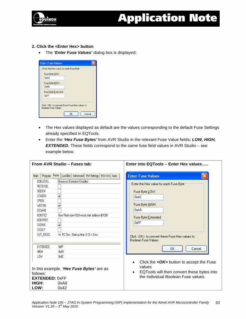
Application Note 105 – JTAG In-System Programming (ISP) Implementation for the Atmel AVR Microcontroller Family Version: V1.20 – 3rd May 2010
53
2. Click the <Enter Hex> button
• The ‘Enter Fuse Values’ dialog box is displayed:
• The Hex values displayed as default are the values corresponding to the default Fuse Settings
already specified in EQTools. • Enter the ‘Hex Fuse Bytes’ from AVR Studio in the relevant Fuse Value fields: LOW, HIGH,
EXTENDED. These fields correspond to the same fuse field values in AVR Studio – see example below.
From AVR Studio – Fuses tab:
In this example, ‘Hex Fuse Bytes’ are as follows: EXTENDED: 0xFF HIGH: 0xA9 LOW: 0x42
Enter into EQTools – Enter Hex values…..
• Click the <OK> button to accept the Fuse values
• EQTools will then convert these bytes into the Individual Boolean Fuse values.
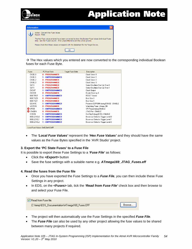
Application Note 105 – JTAG In-System Programming (ISP) Implementation for the Atmel AVR Microcontroller Family Version: V1.20 – 3rd May 2010
54
The Hex values which you entered are now converted to the corresponding individual Boolean fuses for each Fuse Byte.
• The ‘Local Fuse Values’ represent the ‘Hex Fuse Values’ and they should have the same values as the Fuse Bytes specified in the ‘AVR Studio’ project.
3. Export the ‘PC State Fuses’ to a Fuse File It is possible to export these Fuse Settings to a ‘Fuse File’ as follows:
• Click the <Export> button • Save the fuse settings with a suitable name e.g. ATmega169_JTAG_Fuses.eff
4. Read the fuses from the Fuse file
• Once you have exported the Fuse Settings to a Fuse File, you can then include these Fuse Settings in any project.
• In EDS, on the <Fuses> tab, tick the ‘Read from Fuse File’ check box and then browse to and select your Fuse File.
• The project will then automatically use the Fuse Settings in the specified Fuse File. • The Fuse File can also be used by any other project allowing the fuse values to be shared
between many projects if required.
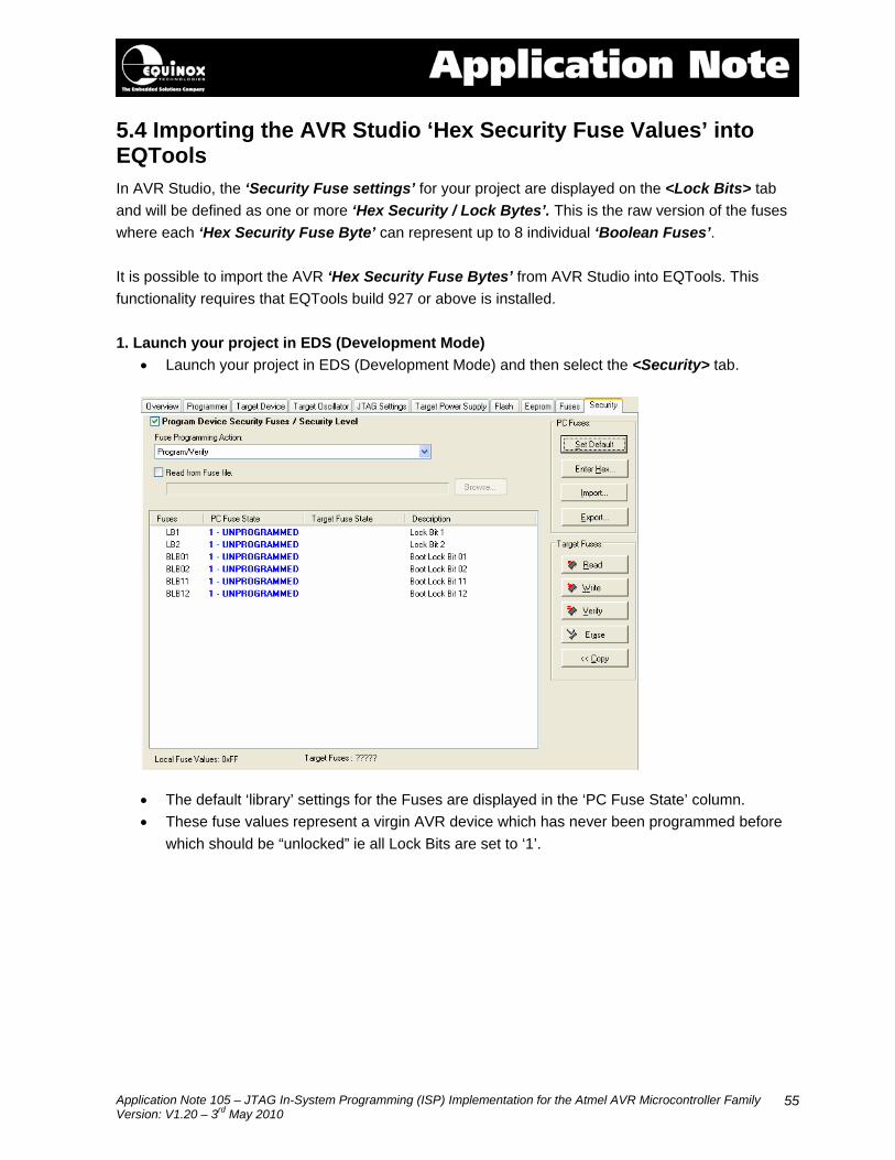
Application Note 105 – JTAG In-System Programming (ISP) Implementation for the Atmel AVR Microcontroller Family Version: V1.20 – 3rd May 2010
55
5.4 Importing the AVR Studio ‘Hex Security Fuse Values’ into EQTools In AVR Studio, the ‘Security Fuse settings’ for your project are displayed on the <Lock Bits> tab and will be defined as one or more ‘Hex Security / Lock Bytes’. This is the raw version of the fuses where each ‘Hex Security Fuse Byte’ can represent up to 8 individual ‘Boolean Fuses’. It is possible to import the AVR ‘Hex Security Fuse Bytes’ from AVR Studio into EQTools. This functionality requires that EQTools build 927 or above is installed. 1. Launch your project in EDS (Development Mode)
• Launch your project in EDS (Development Mode) and then select the <Security> tab.
• The default ‘library’ settings for the Fuses are displayed in the ‘PC Fuse State’ column. • These fuse values represent a virgin AVR device which has never been programmed before
which should be “unlocked” ie all Lock Bits are set to ‘1’.
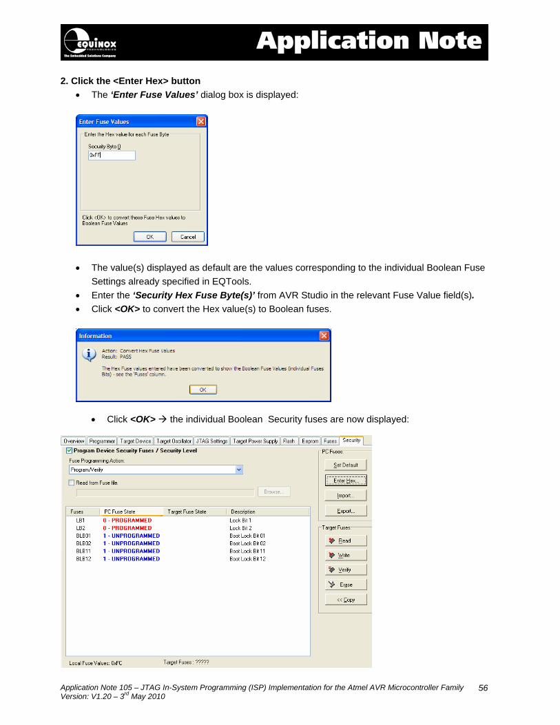
Application Note 105 – JTAG In-System Programming (ISP) Implementation for the Atmel AVR Microcontroller Family Version: V1.20 – 3rd May 2010
56
2. Click the <Enter Hex> button • The ‘Enter Fuse Values’ dialog box is displayed:
• The value(s) displayed as default are the values corresponding to the individual Boolean Fuse Settings already specified in EQTools.
• Enter the ‘Security Hex Fuse Byte(s)’ from AVR Studio in the relevant Fuse Value field(s). • Click <OK> to convert the Hex value(s) to Boolean fuses.
• Click <OK> the individual Boolean Security fuses are now displayed:
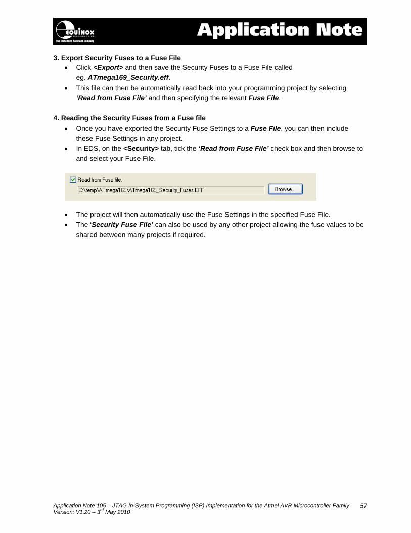
Application Note 105 – JTAG In-System Programming (ISP) Implementation for the Atmel AVR Microcontroller Family Version: V1.20 – 3rd May 2010
57
3. Export Security Fuses to a Fuse File • Click <Export> and then save the Security Fuses to a Fuse File called
eg. ATmega169_Security.eff. • This file can then be automatically read back into your programming project by selecting
‘Read from Fuse File’ and then specifying the relevant Fuse File. 4. Reading the Security Fuses from a Fuse file
• Once you have exported the Security Fuse Settings to a Fuse File, you can then include these Fuse Settings in any project.
• In EDS, on the <Security> tab, tick the ‘Read from Fuse File’ check box and then browse to and select your Fuse File.
• The project will then automatically use the Fuse Settings in the specified Fuse File. • The ‘Security Fuse File’ can also be used by any other project allowing the fuse values to be
shared between many projects if required.

Application Note 105 – JTAG In-System Programming (ISP) Implementation for the Atmel AVR Microcontroller Family Version: V1.20 – 3rd May 2010
58

Application Note 105 – JTAG In-System Programming (ISP) Implementation for the Atmel AVR Microcontroller Family Version: V1.20 – 3rd May 2010
59
6.0 Creating a Standalone Programming Project 6.1 Overview Once you have tested your project fully in EDS (Development Mode), it is possible to then make this project into a ‘Standalone Project’ which can be uploaded to a programmer. This single standalone project file (*.prj) will contain all the information required to program the Target Device including FLASH file, EEPROM file, Fuse settings, Security Settings etc. 6.2 Creating a Standalone Project from EDS (Development Mode) In EDS (Development Mode), select the <Overview> tab
• If this is the first time the EDS Project has been uploaded to a programmer, click the <Add Project File to a new Project Collection> button.
• If the EDS Project has already been uploaded to a programmer before, click the <Update this project in an existing Project Collection> button.
6.3 Add Project File to a new Project Collection When the <Add Project File to a new Project Collection> button is pressed, the EDS project will be automatically added to a new ‘Project Collection’.
• The EDS Project will appear in a ‘Project Manager’ window. • You will then be prompted to save the ‘Project Collection’. Choose a suitable name eg.
Test.ppc and click the <Save> button.

Application Note 105 – JTAG In-System Programming (ISP) Implementation for the Atmel AVR Microcontroller Family Version: V1.20 – 3rd May 2010
60
The Project Manager window is now displayed – see section 6.4. 6.4 Uploading a Project to a programmer The Project Manager window displays all the projects in your Project Collection.
In this example we have only one project called ‘ATMEGA2560-JTAG’. The ‘Unique ID’ is the ‘Project Name’ which is also the file name you saved the project with in EDS. To upload the project to the programmer:
• Click the <Upload all projects> button uploads all the projects in the collection to the programmer.
or • Click once on the project you wish to upload in the Project Manager window and then click
the <Upload selected project> button uploads only the selected project in the collection to the programmer.
Follow the on-screen Upload Wizard instructions to complete the uploading of the project(s) to the programmer(s).
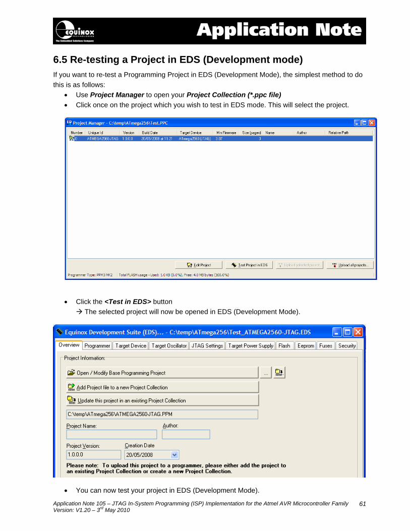
Application Note 105 – JTAG In-System Programming (ISP) Implementation for the Atmel AVR Microcontroller Family Version: V1.20 – 3rd May 2010
61
6.5 Re-testing a Project in EDS (Development mode) If you want to re-test a Programming Project in EDS (Development Mode), the simplest method to do this is as follows:
• Use Project Manager to open your Project Collection (*.ppc file) • Click once on the project which you wish to test in EDS mode. This will select the project.
• Click the <Test in EDS> button
The selected project will now be opened in EDS (Development Mode).
• You can now test your project in EDS (Development Mode).


![App Development Guide for Samsung Smart TV[V1.20]](https://img.pdfslide.us/doc/110x75/577d20981a28ab4e1e93420d/app-development-guide-for-samsung-smart-tvv120.jpg)


![App Development Guide for Samsung Smart TV[V1.20][1]](https://img.pdfslide.us/doc/110x75/55cf9b01550346d033a45bc7/app-development-guide-for-samsung-smart-tvv1201-562d0fc082eb0.jpg)

![App Development Guide for Samsung Smart TV[V1.20][1] 3](https://img.pdfslide.us/doc/110x75/545f337cb1af9feb588b4b39/app-development-guide-for-samsung-smart-tvv1201-3.jpg)