Embed Size (px)
Citation preview

2021.12
ANALOG ICsHigh-performance solutions for precision signal chain design

CONTENTS
Winning Combos ...................................................................... 04
InterfaceInterface ................................................................................... 05
Amplifiers
Precision Op Amps.................................................................... 09Bipolar & CMOS Op Amps/Comparators ................................. 12
Current Sensing ........................................................................ 14
OptoelectronicsPhotocouplers .......................................................................... 16
TimingReal-Time Clocks ...................................................................... 18
Data ConvertersHigh Speed ADC/DACs ............................................................ 19
Precision Data Converters ........................................................ 20
Digital Potentiometers Portfolio ............................................... 21
Voltage References .................................................................. 22
Switches & MultiplexersAnalog Switches ...................................................................... 23
ANALOG ICsHIGH-PERFORMANCE SOLUTIONS FOR PRECISION SIGNAL CHAIN DESIGN
02-03
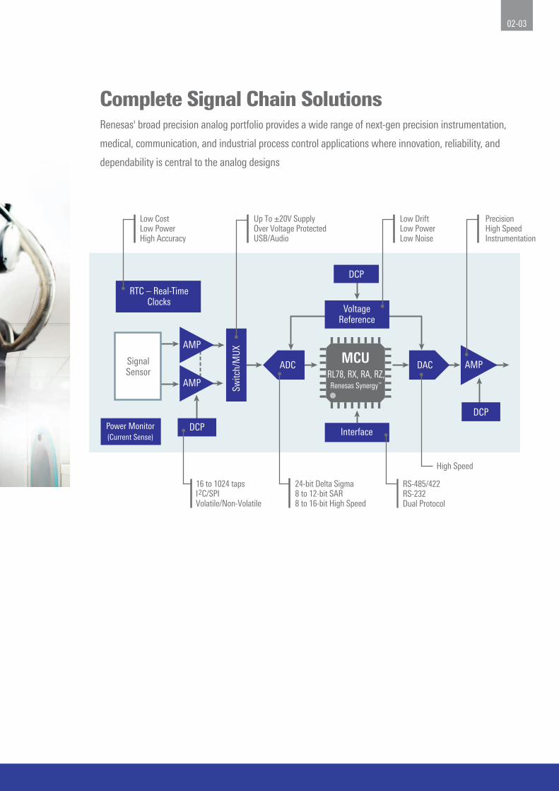
Complete Signal Chain Solutions
RTC – Real-Time Clocks
Signal Sensor
AMP
AMP
DCP
DCP
ADC DAC
Interface
DCP
AMP
VoltageReference
Switc
h/M
UX
Power Monitor(Current Sense)
RL78, RX, RA, RZ, Renesas Synergy™
MCU
PrecisionHigh SpeedInstrumentation
High Speed
Low DriftLow PowerLow Noise
Up To ±20V SupplyOver Voltage ProtectedUSB/Audio
RS-485/422RS-232Dual Protocol
24-bit Delta Sigma8 to 12-bit SAR8 to 16-bit High Speed
Low CostLow PowerHigh Accuracy
16 to 1024 tapsI2C/SPIVolatile/Non-Volatile
Renesas' broad precision analog portfolio provides a wide range of next-gen precision instrumentation,
medical, communication, and industrial process control applications where innovation, reliability, and
dependability is central to the analog designs
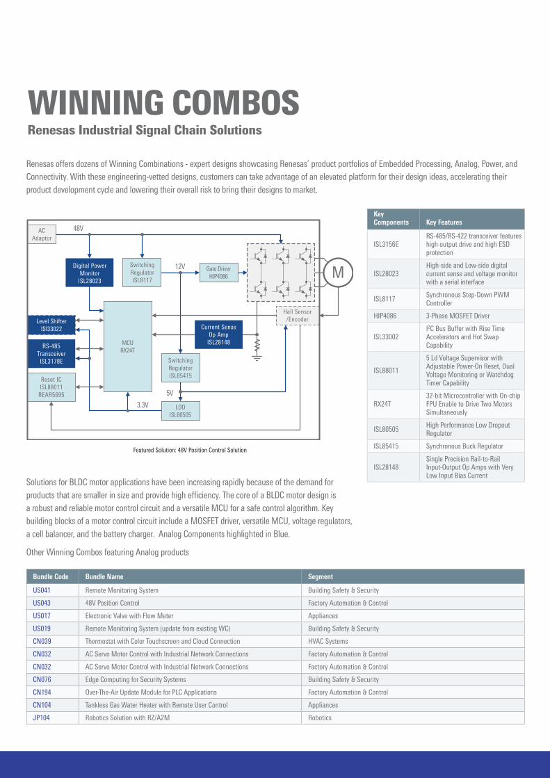
WINNING COMBOSRenesas Industrial Signal Chain Solutions
Renesas offers dozens of Winning Combinations - expert designs showcasing Renesas’ product portfolios of Embedded Processing, Analog, Power, and Connectivity. With these engineering-vetted designs, customers can take advantage of an elevated platform for their design ideas, accelerating their product development cycle and lowering their overall risk to bring their designs to market.
Solutions for BLDC motor applications have been increasing rapidly because of the demand for products that are smaller in size and provide high efficiency. The core of a BLDC motor design is a robust and reliable motor control circuit and a versatile MCU for a safe control algorithm. Key building blocks of a motor control circuit include a MOSFET driver, versatile MCU, voltage regulators, a cell balancer, and the battery charger. Analog Components highlighted in Blue.
Other Winning Combos featuring Analog products
Featured Solution: 48V Position Control Solution
Bundle Code Bundle Name Segment
US041 Remote Monitoring System Building Safety & Security
US043 48V Position Control Factory Automation & Control
US017 Electronic Valve with Flow Meter Appliances
US019 Remote Monitoring System (update from existing WC) Building Safety & Security
CN039 Thermostat with Color Touchscreen and Cloud Connection HVAC Systems
CN032 AC Servo Motor Control with Industrial Network Connections Factory Automation & Control
CN032 AC Servo Motor Control with Industrial Network Connections Factory Automation & Control
CN076 Edge Computing for Security Systems Building Safety & Security
CN194 Over-The-Air Update Module for PLC Applications Factory Automation & Control
CN104 Tankless Gas Water Heater with Remote User Control Appliances
JP104 Robotics Solution with RZ/A2M Robotics
Key Components Key Features
ISL3156ERS-485/RS-422 transceiver features high output drive and high ESD protection
ISL28023High-side and Low-side digital current sense and voltage monitor with a serial interface
ISL8117 Synchronous Step-Down PWM Controller
HIP4086 3-Phase MOSFET Driver
ISL33002I2C Bus Buffer with Rise Time Accelerators and Hot Swap Capability
ISL88011
5 Ld Voltage Supervisor with Adjustable Power-On Reset, Dual Voltage Monitoring or Watchdog Timer Capability
RX24T32-bit Microcontroller with On-chip FPU Enable to Drive Two Motors Simultaneously
ISL80505 High Performance Low Dropout Regulator
ISL85415 Synchronous Buck Regulator
ISL28148Single Precision Rail-to-Rail Input-Output Op Amps with Very Low Input Bias Current
Gate DriverHIP4086
Current SenseOp Amp
ISL28148
SwitchingRegulatorISL8117
M
Hall Sensor/Encoder
SwitchingRegulatorISL85415
LDOISL80505
RS-485TransceiverISL3178E
MCURX24T
Level ShifterISl33022
12V
5V
Reset ICISL88011
REAR5695
3.3V
48VACAdaptor
Digital PowerMonitor
ISL28023
04-05
RAA
7881
5x
RAA
7881
5x
2.4V
1.9V
3.1V
5kV4kV
2kV
Dri
ver
Out
put
Volta
ge
EFT Imm
unity
Com
petit
or A
Com
petit
or B
Com
petit
or A
Com
p. B
Transceiver Noise Immunity
2.7
Supp
ly C
urre
nt (A
)
2.8 2.9 3.0 3.1 3.2 3.3 3.4 3.5 3.610µ
100µ
1m
Supply Voltage (V)
ISL3260xE
ISL3172E
10kbps
Idle
10kbps
Idle
Broad Portfolio to Fit Your Needs
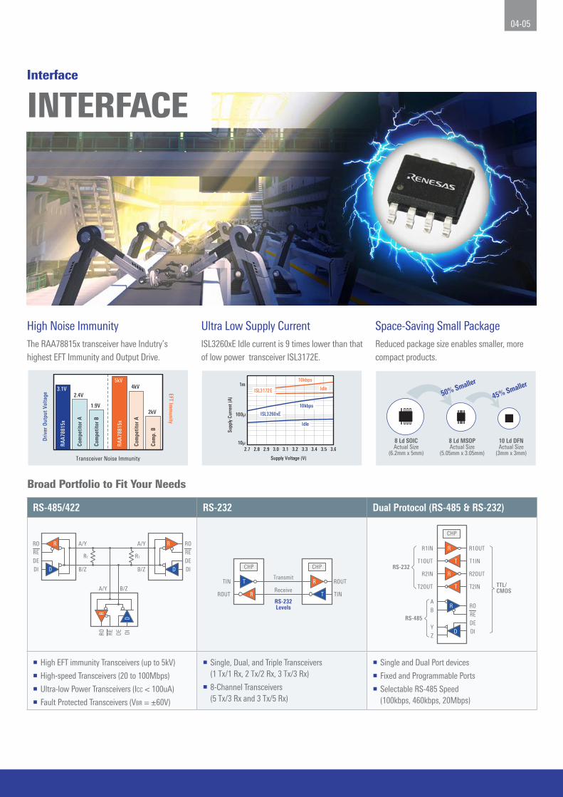
INTERFACE
High Noise ImmunityThe RAA78815x transceiver have Indutry’s highest EFT Immunity and Output Drive.
Ultra Low Supply CurrentISL3260xE Idle current is 9 times lower than that of low power transceiver ISL3172E.
Space-Saving Small PackageReduced package size enables smaller, more compact products.
50% Smaller
45% Smaller
8 Ld SOICActual Size
(6.2mm x 5mm)
8 Ld MSOPActual Size
(5.05mm x 3.05mm)
10 Ld DFNActual Size
(3mm x 3mm)
RS-485/422 RS-232 Dual Protocol (RS-485 & RS-232)
RO R
D
RE
DE
DI
A/Y
B/Z
RT
ROR
D
RE
DE
DI
A/Y
B/Z
RT
ROR
D
RE DE DI
A/Y B/Z
Transmit
Receive
RS-232Levels
CHP
R
TTIN
ROUT
CHP
R
T TIN
ROUT
CHP
R
T T1IN
R1OUT
R
T T2IN
R2OUT
ROR
D
REDEDI
A
B
YZ
T1OUT
R1IN
T2OUT
R2INRS-232
RS-485
TTL/CMOS
¡ High EFT immunity Transceivers (up to 5kV)
¡ High-speed Transceivers (20 to 100Mbps)
¡ Ultra-low Power Transceivers (ICC < 100uA)
¡ Fault Protected Transceivers (VBR = ±60V)
¡ Single, Dual, and Triple Transceivers (1 Tx/1 Rx, 2 Tx/2 Rx, 3 Tx/3 Rx)
¡ 8-Channel Transceivers (5 Tx/3 Rx and 3 Tx/5 Rx)
¡ Single and Dual Port devices
¡ Fixed and Programmable Ports
¡ Selectable RS-485 Speed (100kbps, 460kbps, 20Mbps)
Interface

RS-485/RS-422 TransceiversRS-485 is a multi-point interface bus, meaning multiple drivers and receivers can be connected to one bus. RS-485 uses differential signaling to achieve high noise immunity. Its common-mode voltage range reaches from -7V up to +12V.
RS-422 is a multi-drop interface bus, meaning only one driver but multiple receivers can connect to one bus. RS-422 also uses differential signaling. Its common-mode voltage range however is smaller and ranges from -7V up to +7V.
Note that RS-485 transceiver can be used in RS-422 networks but not vice versa. RS-422 devices cannot be used in RS-485 systems.
Renesas has a 50-year history in interface transceivers and we are still a market leader today. We have a full portfolio of RS-485/RS-422 transceivers suited to most design needs.
Transceivers with High EFT Immunity per IEC61000-4-2Transceiver Family VCC Range (V) EFT (kV) Data Rates
(Mbps) VOD (typ) (V) # Devices on bus
Half / Full Duplex
Bus ESD HD / FD (kV)
Quiescent ICC (µA)(RX = on)
Temp Range (ºC)
RAA78815x 4.5 – 5.5 5 0.115 / 1 / 20 3.1 256 HD / FD 16.5 / 10 550 -40 to +85
ISL315xE 4.5 – 5.5 2 0.115 / 1 / 20 3.1 256 HD / FD 16.5 / 10 550 -40 to +85
ISL317xE 3.0 – 3.6 2 0.25 / 0.5 / 20 2.0 256 HD / FD 16.5 / 10 480 -40 to +85
x = 0,2,3,5,6,8
High-Speed Transceivers (DR ≥ 40Mbps)
Part Number VCC Range (V) Data Rate (Mbps) VOD (typ)(V) Half / Full
Duplex
Devices allowed on bus
Hot Plug IEC ESD (kV) ICC (mA) ISHDN (µA) Temp Range (ºC)
ISL3179E 3.0 – 3.6 40 2.0 Half 160 Yes ±16.5 2.6 0.05 -40 to +125
ISL3180E 3.0 – 3.6 40 2.0 Full 160 Yes ±5 2.6 0.05 -40 to +85
ISL3159E 4.5 – 5.5 40 2.8 Half 160 Yes ±15 2.6 0.05 -40 to +125
ISL3160E 4.5 – 5.5 40 2.8 Full 160 Yes ±5 2.6 1.4 -40 to +125
ISL3259E 4.5 – 5.5 100 2.8 Half 160 Yes ±15 2.6 0.05 -40 to +85
Ultra-Low Power Transceivers
Part Number # TX # RX VCC Range (V) Data Rates (kbps) Duplex
# Devices allowed on bus
Bus ESD (kV) Quiescent ICC (µA) ISHDN (µA) Temp Range
(ºC)
ISL32600E 1 1 2.7 – 3.6 256 Full 256 ±15 70 0.01 -40 to +125
ISL32601E 1 1 2.7 – 3.6 256 Half 256 ±15 70 0.01 -40 to +125
ISL32603E 1 1 1.8 – 3.6 460 Half 256 ±15 150 0.01 -40 to +125
ISL32612E 0 1 1.8 – 3.3 256 / 500 – 256 ±16.5 85 – -40 to +125
ISL32614E 1 0 1.8 – 3.3 128 / 256 – 256 ±16.5 100 0.01 -40 to +125
Single RS-485/422 Drivers and Receivers
Part Number # TX # RX VCC Range (V) Data Rate (Mbps) VOD (typ) (V) VL Pin (V) TX / RX
Enables IEC ESD (kV) ICC (µA) Temp Range (ºC)
ISL3295E 1 0 3.0 – 5.5 20 2.0 (Vcc = 3.0V) 3.4 (Vcc = 4.5V) – Active High ±16.5 120 -40 to +125
ISL3298E 1 0 3.0 – 5.5 20 2.0 (Vcc = 3.0V) 3.4 (Vcc = 4.5V) 1.6 Active High ±16.5 120 -40 to +125
ISL3280E 0 1 3.0 – 5.5 20 – – None ±16.5 400 -40 to +125
ISL3281E 0 1 3.0 – 5.5 20 – – Active High ±16.5 400 -40 to +125
ISL3282E 0 1 3.0 – 5.5 20 – 1.6 Active Low ±16.5 400 -40 to +125
ISL3283E 0 1 3.0 – 5.5 20 – – Active Low ±16.5 400 -40 to +125

06-07
Overvoltage Protected Transceivers
Part Number VCC Range (V) OVP (V) CMVR (V) Half / Full Duplex
Data Rates (Mbps)
Devices allowed on bus
Hot Plug IEC ESD (kV) ICC /ISHDN (mA)
Temp Range (ºC)
ISL3243xE 3.0 – 5.5 ±40 ±15 HD / FD 0.25 / 1.0 128 No ±15 2.1 / 0.01 -40 to +85
ISL3245xE 3.0 – 5.5 ±60 ±20 HD / FD 0.25 / 1 / 20 128 No ±15 2.1 / 0.01 -40 to +85
ISL3247xE 4.5 – 5.5 ±60 ±15 HD / FD 0.25 / 1 / 15 128 Yes ±16.5 2.3 / 0.01 -40 to +85
ISL3249xE 4.5 – 5.5 ±60 ±25 HD / FD 0.25 / 1 / 15 128 Yes ±16.5 2.3 / 0.01 -40 to +85
x = 0,2,3,5,6,8
Quad RS-422 Drivers and RS-485/422 Receivers
Part Number # TX # RX VCC Range (V) Data Rate (Mbps) VOD (typ) (V) VL Pin (V) TX / RX Enables IEC ESD (kV) ICC (µA) Temp Range
(ºC)
RAA7884QT 4 0 3.0 – 5.5 50 2.6 (Vcc = 3.0V)4.0 (Vcc = 4.5V) – Group ±16.5 0.8 -40 to +125
ISL32172E 4 0 3.0 – 5.5 32 2.6 (Vcc = 3.0V)4.0 (Vcc = 4.5V) – Group ±16.5 0.6 -40 to +125
ISL32272E 4 0 3.0 – 5.5 10 2.6 (Vcc = 3.0V)4.0 (Vcc = 4.5V) – Group ±16.5 0.6 -40 to +125
ISL32174E 4 0 3.0 – 5.5 32 2.6 (Vcc = 3.0V)4.0 (Vcc = 4.5V) – Paired ±16.5 0.6 -40 to +125
ISL32179E 4 0 3.0 – 5.5 32 2.6 (Vcc = 3.0V)4.0 (Vcc = 4.5V) 1.6 Individual &
Group ±16.5 0.6 -40 to +125
ISL32173E 0 4 3.0 – 5.5 80 – – Group ±16.5 15 -40 to +125
ISL32177E 0 4 3.0 – 5.5 80 – 1.6 Individual & Group ±16.5 15 -40 to +125
ISL32273E 0 4 3.0 – 5.5 20 – – Group ±16.5 5.5 -40 to +125
ISL32275E 0 4 3.0 – 5.5 20 – – Paired ±16.5 5.5 -40 to +125
ISL32277E 0 4 3.0 – 5.5 20 – 1.6 Individual & Group ±16.5 5.5 -40 to +125
RAA7884QR 0 4 3.0 – 5.5 80 – – Group ±16.5 15 -40 to +125
RS-232 TransceiversRS-232 is a point-to-point interface between two RS-232 transceivers. RS-232 using single-ended signaling but with positive and negative voltages, such as ±5V to ±13V.
RS-232 Transceivers with Single, Dual, and Triple ChannelsPart Number Data Rate(Mbps) VCC (V) Shutdown* Man./Auto High ESD (kV) Temp Range (ºC) Package
SINGLE TRANSCEIVER ( 1 Tx / 1 Rx )
ICL3221E 0.5 3 – 5 A (B) 15 -40 to +85 SSOP16, TSSOP16
ICL3221EM 0.5 3 A (B) 15 -55 to +125 TSSOP16
ICL3226E 0.5 3 – 5 A (E) 15 -40 to +85 SSOP16
DUAL TRANSCEIVERS ( 2 Tx / 2 Rx )
ICL3222E 0.5 3 – 5 M 15 -40 to +85 SOIC18, SSOP20, TSSOP20
ICL3223E 0.5 3 – 5 A (B) 15 -40 to +85 SSOP20, TSSOP20
ICL3224E 0.5 3 – 5 A (E) 15 -40 to +85 SSOP20
ICL3225E 1 3 – 5 A (E) 15 -40 to +85 SSOP20
ICL3232E 0.5 3 – 5 M 15 -40 to +125 SOIC16, SSOP16, TSSOP16, TSSOP20
ISL3232E 0.5 3 – 5 M 15 -40 to +85 QFN16
ISL4223E 0.5 3 – 5 A (B) 15 -40 to +85 QFN20
TRIPPLE TRANSCEIVERS ( 3 Tx / 3 Rx )
ISL4270E 0.5 3.0 – 5.5 A (E) 15 -40 to +85 QFN32
ISL83387E 0.5 3.0 – 5.5 A (E) 15 -40 to +85 TSSOP24
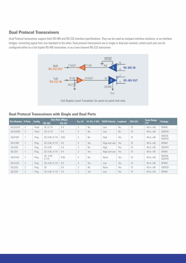
Dual Protocol TransceiversDual Protocol transceivers support both RS-485 and RS-232 interface specifications. They can be used as compact interface solutions, or as interface bridges, converting signal from one standard to the other. Dual protocol transceivers are in single or dual port variants, where each port can be configured either as a full duplex RS-485 transceiver, or as a two-channel RS-232 transceiver.
Dual Protocol Transceivers with Single and Dual Ports
Part Number # Ports Config.Data Rate (Mbps)
VCC (V) VL-Pin (1.8V) RXEN Polarity Loopback ESD (kV) Temp Range (ºC) Package
RS-485 RS-232
ISL33337E 2 Fixed 20, 0.115 0.4 3 No Low No 15 -40 to +85 QFN40
ISL33354E 2 Fixed 20, 0.115 0.4 5 No Low No 15 -40 to +85 SSOP28
ISL81387 1 Prog. 20, 0.46, 0.115 0.65 5 No High Yes 15 -40 to +85 SOIC20, SSOP20
ISL41387 1 Prog. 20, 0.46, 0.115 0.5 5 Yes High and Low Yes 15 -40 to +85 QFN40
ISL3330 1 Prog. 20, 0.46 0.4 3 No High Yes 15 -40 to +85 SSOP20
ISL3331 1 Prog. 20, 0.46, 0.115 0.4 3 Yes High and Low Yes 15 -40 to +85 QFN40
ISL81334 2 Prog. 20 , 0.46 , 0.115 0.65 5 No None Yes 15 -40 to +85 SOIC28,
SSOP28
ISL41334 2 Prog. 20, 0.46, 0.115 0.5 5 Yes Low Yes 15 -40 to +85 QFN40
ISL3332 2 Prog. 20 0.4 3 No None Yes 15 -40 to +85 SSOP28
ISL3333 2 Prog. 20, 0.46, 0.115 0.4 3 Yes Low Yes 15 -40 to +85 QFN40
Full-Duplex Level Translator for point-to-point link only
R1IN R1OUT
T1IN
TxDRS-232 IN
RxDRS-232 OUT
Y
Z
A
B
DI
DE485
RO
RE485
D R
DR
Vcc
RS-485 OUT
RS-485 IN
5kΩ
T1OUT
08-09
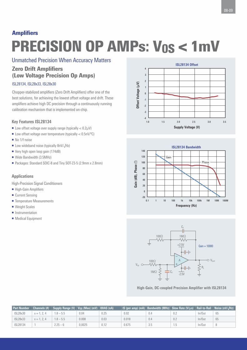
Zero Drift Amplifiers (Low Voltage Precision Op Amps)ISL28134, ISL28x33, ISL28x30
Chopper-stabilized amplifiers (Zero Drift Amplifiers) offer one of the best solutions, for achieving the lowest offset voltage and drift. These amplifiers achieve high DC precision through a continuously running calibration mechanism that is implemented on-chip.
PRECISION OP AMPs: V0S < 1mVAmplifiers
Unmatched Precision When Accuracy Matters
Key Features ISL28134 ¡ Low offset voltage over supply range (typically < 0.2µV)
¡ Low offset voltage over temperature (typically < 0.5nV/ºC)
¡ No 1/f noise
¡ Low wideband noise (typically 8nV/√Hz)
¡ Very high open loop gain (174dB)
¡ Wide Bandwidth (3.5MHz)
¡ Packages: Standard SOIC-8 and Tiny SOT-23-5 (2.9mm x 2.8mm)
Applications
High-Precision Signal Conditioners¡ High-Gain Amplifiers
¡ Current Sensing
¡ Temperature Measurements
¡ Weight Scales
¡ Instrumentation
¡ Medical Equipment
Part Number Channels (#) Supply Range (V) VOS (Max) (mV) IBIAS (nA) IS (per amp) (mA) Bandwidth (MHz) Slew Rate (V/µs) Rail-to-Rail Noise (nV/√Hz)
ISL28x30 x = 1, 2, 4 1.8 – 5.5 0.04 0.25 0.02 0.4 0.2 In/Out 65
ISL28x33 x = 1, 2, 4 1.8 – 5.5 0.008 0.03 0.018 0.4 0.2 In/Out 65
ISL28134 1 2.25 – 6 0.0025 0.12 0.675 3.5 1.5 In/Out 8
ISL28134 Offset
Supply Voltage (V)
3.53.02.52.01.51.0
Off
set V
olta
ge (µ
V)
4
3
2
1
0
-1
-2
-3
-4
10.1 10010 10k1k 1M100k 100M10M
Frequency (Hz)
Gain
(dB)
, Pha
se (˚
)
140
120
100
80
60
40
20
0
-20
Gain
Phase
ISL28134 Bandwidth
A
CF1MΩ
+2.5V
VIN
-2.5V
100Ω
1MΩ100Ω
CF
RL
VOUT
Gain = 10000
High-Gain, DC-coupled Precision Amplifier with ISL28134

Amplifiers
High-Voltage Precision Op-AmpsOur high-voltage precision amplifiers feature low noise, high slew rate, and very low offset voltage, making them the ideal choice for applications where precision and low noise are important, such as precision medical and analytical instrumentation, sensor conditioning, precision power supply controls, industrial controls, and photodiode amplifiers. All devices operate over the extended temperature range from -40°C to +125°C.
General Purpose Op-AmpsAll general-purpose op-amps feature ground sensing capability. Most op-amps, however, possess rail-to-rail capability to enhance the dynamic input and output signal range and thus, signal integrity. Amongst these amplifiers, the ultra-low power op-amp, ISL28194, has a supply current of only 330nA, which makes it ideal for battery-powered applications.
Part Number Channels (#) Supply Range (V) Vos (Max) (mV) IBIAS (nA) IS (per amp)
(mA)Bandwidth (MHz)
Slew Rate (V/µs) Noise (nV/√Hz) Temperature
Range (ºC)
ISL28x07 x = 2, 4 4.5 – 40 0.075 0.015 0.21 1 0.32 13 -40 to 125
ISL28x08 x = 1, 2, 4 3 – 40 0.15 -13 0.185 1.2 0.45 16 -40 to 125
ISL28x10 x = 1, 2 9 – 40 0.3 0.0003 2.55 12.5 23 6 -40 to 125
ISL28x17 x = 2, 4 4.5 – 40 0.05 1 0.44 1.5 0.5 8 -40 to 125
ISL28x18 x = 1, 2 3 – 40 0.15 -230 0.85 4 1.2 5.6 -40 to 125
ISL28x27 x = 1, 2 4.5 – 40 0.07 10 2.8 10 3.6 2.5 -40 to 125
ISL28177 1 4.5 – 40 0.15 0.2 1.18 0.6 0.2 9.5 -40 to 125
Part Number Channels (#) Supply Range (V) Vos (Max) (mV) IBIAS (nA) IS (per amp)
(mA)Bandwidth (MHz)
Slew Rate (V/µs) Rail-to-Rail Temperature
Range (ºC)
CA3130 1 5 – 16 5 0.005 2 15 30 -Vs -55 to +125
CA3140 1 4 – 36 5 0.01 4 4.5 9 -Vs -55 to +125
EL5x20 x = 2, 4 4.5 – 16.5 12 50 0.75 12 10 In/Out -40 to +125
EL5420T 4 4.5 – 19 13 50 0.75 12 12 In/Out -40 to +85
ISL24021 1 4.5 – 19 15 10 2.8 25 18 In/Out -40 to +85
ISL28x13 x = 1, 2, 4 1.8 – 5.5 5 0.003 0.13 2 1 In/Out -40 to +125
ISL28x14 x = 1, 2, 4 1.8 – 5.5 5 0.003 0.039 5 2.5 In/Out -40 to +125
ISL28194 1 1.8 – 5.5 2.5 0.015 0.00033 0.0035 0.0012 In/Out -40 to +125

10-11
High-Speed Op-AmpsOur high-speed op-amps include amplifiers with low offset and rail-to-rail outputs for precision applications, high slew rate devices, and fully differential amplifiers with ultra-low distortion for driving high-speed ADCs.
Part Number Channels (#) Topology Supply Range (V)
Bandwidth (MHz)
Slew Rate (V/µs)
Noise (nV/√Hz) 2nd HD (dB) 3rd HD (dB) IS per amp
(mA)VOS (Max) (mV)
Voltage Feedback Amplifiers with Rail-to-Rail Outputs
ISL28191 1 VFA 3 – 5.5 61 17 1.7 -76 -70 2.6 0.63
ISL28291 2 VFA 3 – 5.5 61 17 1.7 -76 -70 2.6 0.63
EL8101 1 VFA 3 – 5 200 200 10 -62 -65 2 6
EL8201 2 VFA 3 – 5.5 200 200 10 -62 -65 2 6
Voltage Feedback Amplifiers with Enhanced Slew Rate
EL5203 2 VFA 5 – 10 400 2200 12 -76 -75 5.2 5
ISL55001 1 VFA 5 – 30 220 300 12 -72 -80 9 3
ISL55002 2 VFA 5 – 30 200 300 12 -72 -80 8.5 5
Fully Differential Amplifiers
ISL55210 1 FDA 3 – 4.2 2200 5600 0.85 -105 -120 35 1.4
Current Feedback Amplifiers
EL5160 1 CFA 5 – 10 200 1700 4 -74 -50 0.75 5
EL5161 1 CFA 5 – 10 200 1700 4 -74 -50 0.75 5
EL5x62 x = 1, 2, 4 CFA 5 – 12 500 4000 3 1.5 5
EL5x63 x = 1, 2 CFA 5 – 12 500 2500 3 1.5 5
EL5x64 x = 1, 3 CFA 5 – 12 600 4700 2.1 -81 -74 5 5
EL5166 1 CFA 5 – 12 1400 6000 1.7 -70 -78 8.5 5
Differential Line Drivers and Receivers
EL5171 1 VFA 5 – 11 250 800 26 -94 -77 8 25
EL5172 1 VFA 5 – 11 250 800 26 -59 -60 6 25
EL5174 1 VFA 5 – 11 550 1100 21 -95 -88 12.5 25
EL5x75 x = 1, 3 VFA 5 – 11 550 900 21 -65 -78 9.6 40
EL5177 1 VFA 5 – 11 550 1100 21 -95 -88 12.5 25
EL5378 3 VFA 5 – 11 700 1000 18 -83 -88 12.5 30
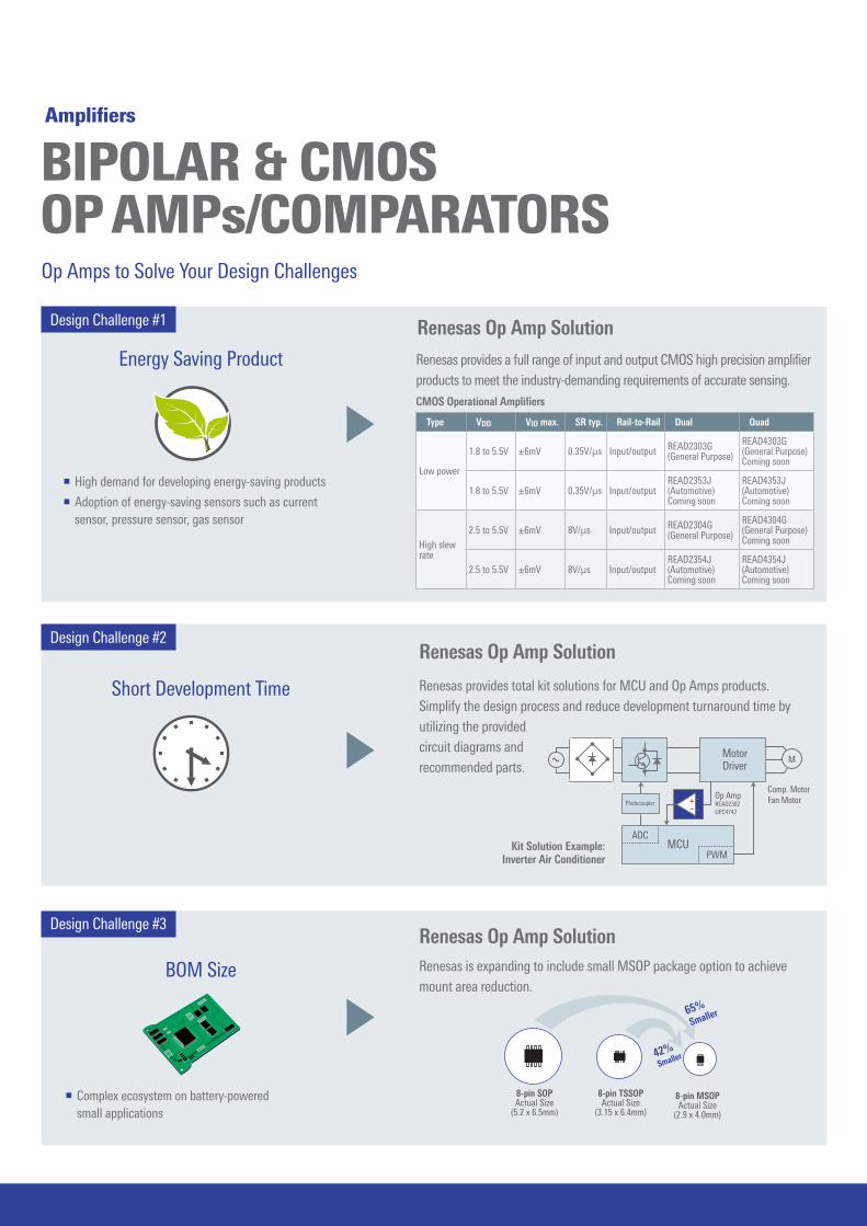
BIPOLAR & CMOS OP AMPs/COMPARATORS
Amplifiers
Design Challenge #1
Design Challenge #2
Design Challenge #3
Renesas Op Amp Solution
Renesas Op Amp Solution
Renesas Op Amp Solution
¡ High demand for developing energy-saving products
¡ Adoption of energy-saving sensors such as current sensor, pressure sensor, gas sensor
¡ Complex ecosystem on battery-powered small applications
Renesas provides a full range of input and output CMOS high precision amplifier products to meet the industry-demanding requirements of accurate sensing.
Renesas provides total kit solutions for MCU and Op Amps products. Simplify the design process and reduce development turnaround time by utilizing the provided circuit diagrams and recommended parts.
Renesas is expanding to include small MSOP package option to achieve mount area reduction.
Type VDD VIO max. SR typ. Rail-to-Rail Dual Quad
Low power
1.8 to 5.5V ±6mV 0.35V/µs Input/output READ2303G (General Purpose)
READ4303G (General Purpose) Coming soon
1.8 to 5.5V ±6mV 0.35V/µs Input/outputREAD2353J (Automotive) Coming soon
READ4353J (Automotive) Coming soon
High slew rate
2.5 to 5.5V ±6mV 8V/µs Input/output READ2304G (General Purpose)
READ4304G (General Purpose) Coming soon
2.5 to 5.5V ±6mV 8V/µs Input/outputREAD2354J (Automotive) Coming soon
READ4354J (Automotive) Coming soon
Energy Saving Product
Short Development Time
BOM Size
65%
Smaller
42%
Smaller
8-pin SOPActual Size
(5.2 x 6.5mm)
8-pin TSSOPActual Size
(3.15 x 6.4mm)
CMOS Operational Amplifiers
8-pin MSOPActual Size
(2.9 x 4.0mm)
MCUADC
PWM
Op AmpREAD2302UPC4742
Photocoupler
MotorDriver
Example: Inverter Air-con.
2.8
2.9
4.0
0.65
MSOP
+-
M
Comp. MotorFan Motor
Kit Solution Example:Inverter Air Conditioner
Op Amps to Solve Your Design Challenges

12-13
Bipolar Operational AmplifiersMost of Industrial's products are also compatible with automotive applications.
Type
Part Number
Power Supply Voltage (V)
VI0 (max)(mV)
ICC (max)(mA)
SR (typ)(V/µs) Channels PackageIndustrial
General Purpose
Single power supply
µPC451 – 3 to 30 ±7 2 0.3 4 14-pin SOP/TSSOP
µPC452 µPC3403 3 to 32 ±7 7 0.8 4 14-pin SOP
µPC842/A µPC4742 3 to 32 ±5 4.5 7 2 8-pin SOP/TSSOP/MSOP*
µPC844 µPC4744 3 to 32 ±5 9 7 4 14-pin SOP/TSSOP
µPC1251 – 3 to 30 ±7 1.2 0.3 2 8-pin SOP/TSSOP/MSOP
REAC1251G – 3 to 30 ±1 1.4 0.3 2 8-pin SOP/TSSOP/MSOP
REAC1251J (Automotive) – 3 to 30 ±1 1.4 0.3 2 8-pin SOP/TSSOP/MSOP
Low noise
µPC258 µPC4558 ±4 to ±16 ±6 5.7 1 2 8-pin SOP
µPC259 µPC4560 ±4 to ±16 ±6 5.7 2.8 2 8-pin SOP
µPC458 µPC4741 ±4 to ±16 ±5 7 1 4 14-pin SOP
– µPC4570 ±4 to ±16 ±5 8 7 2 8-pin SOP/TSSOP
– µPC4572 ±2 to ±7 ±5 7 6 2 8-pin SOP
– µPC4574 ±4 to ±16 ±5 12 6 4 14-pin SOP/TSSOP
J-FET
µPC811 – ±5 to ±16 ±2.5 3.4 15 1 8-pin SOP/TSSOP
µPC812 µPC4092 ±5 to ±16 ±3 6.8 15 2 8-pin SOP/TSSOP
µPC813 – ±5 to ±16 ±2.5 3.5 25 1 8-pin SOP/TSSOP
µPC814 µPC4094 ±5 to ±16 ±3 6.8 25 2 8-pin SOP/TSSOP
µPC822 µPC4072 ±5 to ±16 ±10 5 13 2 8-pin SOP/TSSOP
µPC824 µPC4074 ±5 to ±16 ±10 10 13 4 14-pin SOP/TSSOP
µPC832 µPC4062 ±2 to ±16 ±10 0.5 3 2 8-pin SOP/TSSOP
µPC834 µPC4064 ±2 to ±16 ±10 1 3 4 14-pin SOP/TSSOP
µPC835 – ±5 to ±16 ±3 2.2 5.5 2 8-pin TSSOP
Low power µPC802 – ±1 to ±16 ±6 ≤0.1 ≤1.0 1 8-pin SOP
General µPC251 µPC1458 ±7.5 to ±16 ±6 5.6 0.5 1 8-pin SOP * MSOP corresponds to uPC842A only
Bipolar Comparators
Type
Part NumberPower Supply Voltage (V)
VIO (max)(mV)
ICC (max)(mA)
Tr/Tf (typ)(µs) Channels PackageIndustrial
General Purpose
General
µPC177 – 2 to 32 ±5 2 1.3 4 14-pin SOP/TSSOP
µPC271 – 5 to 32 ±7.5 7.5 0.2 1 8-pin SOP
µPC272 µPC319 5 to 16 ±8 12.5 0.08 2 14-pin SOP
µPC277 – 2 to 32 ±5 1 1.3 2 8-pin SOP/TSSOP/MSOP• Industrial: Products with extended temperature tolerances (125°C).
8-pin 14-pin
SOP (5.2x6.5)
TSSOP (3.15x6.4)
MSOP (2.9x4.0)
MMPAK (2.95x4.0)
SOP (10.2x6.5)
TSSOP (5.2x6.4)
CMOS Operational Amplifiers
Type Rail-to-Rail Part NumberPower Supply Voltage (V)
VIO (max)(mV)
IDD (typ)(µA/ch)
SR typ(V/μs) Channels Package
Low power
Input/output READ2351J (Automotive) 1.8 to 5.5 ±6 40 0.35 2 8-pin TSSOP
Input/output READ2303G (General Purpose) 1.8 to 5.5 ±6 40 0.35 2 8-pin TSSOP/MSOP
Input/output READ2353J (Automotive) 1.8 to 5.5 ±6 40 0.35 2 8-pin TSSOP
Input/output READ4303G (General Purpose) 1.8 to 5.5 ±6 40 0.35 4 14-pin TSSOP
Input/output READ4353J (Automotive) 1.8 to 5.5 ±6 40 0.35 4 14-pin TSSOP
High slew rate
Input/output READ2302G (General Purpose) 2.5 to 5.5 ±6 750 8 2 8-pin TSSOP
Input/output READ2352J (Automotive) 2.5 to 5.5 ±6 750 8 2 8-pin TSSOP
Input/output READ2304G (General Purpose) 2.5 to 5.5 ±6 750 8 2 8-pin TSSOP/MSOP
Input/output READ2354J (Automotive) 2.5 to 5.5 ±6 750 8 2 8-pin TSSOP
Input/output READ4304G (General Purpose) 2.5 to 5.5 ±6 750 8 4 14-pin TSSOP
Input/output READ4354J (Automotive) 2.5 to 5.5 ±6 750 8 4 14-pin TSSOP

CURRENT SENSINGAmplifiers
Current sensing is a fundamental requirement in a wide range of electronic applications. Measuring current drop across a sense resistor is the most commonly used method due to being low cost, having high measurement accuracy, allowing a large measurable current range, and being capable to measure DC and AC currents.
Discrete Solution
A basic current sense amplifier is an op-amp configured as a difference amplifier. The diff-amp rejects the common mode voltage present at the points V1 and V2 and amplifies only the voltage difference across the sense resistor by the circuit gain. A separate reference voltage sets the midpoint of the output voltage around which the amplified input voltage swings. Substituting the voltage difference with the load current times the sense resistance and solving for the load current gives:
IL = (VO - VREF) / (RS · G)
Precision Op Amps for Current Sensing
Most Common Discrete Solutions
Type Part Number TCVOSVOS Max @ 25ºC Notes
Low Noise ISL28290 – 700µV Low cost (low side)
Low Drift ISL28x30 150nV/ºC 40µV Good – still low cost
Zero Drift ISL28x33 75nV/ºC 8µV Great
Zero Drift ISL28134 15nV/ºC 2.5µV World Class
Standard CMOS ISL28113 ISL28114 2µV/ºC 5mV
Standard CMOS READ2302 3µV/ºC 6mV
Example: 20mA Resolution, 5A Full Current Solution VOS RS RS Power Loss Benefits
Generic 500µV 25mΩ 625mW –
ISL28x30 40µV 2mΩ 50mW 92% Power Savings
ISL28134 2.5µV 125µΩ 3mW 99.5% Power Savings
Generic versus High-Precision SolutionUsing a low offset voltage op amp in the sensing circuit allows for a much lower sense resistor and less wasted power.
VCC
VOUTA
RFRG
RFRG
VREF
RS
IL
V1
V2
Bidirectional Current Sensing

14-15
Digital Power Monitors
High Voltage Precision Sensing for Current, Voltage, and Power
Integrated Solution
The ISL28005 and ISL28006 are ground sensing current sense amplifiers that amplify milli-volt current signals developed across sub-1Ω sense resistors. The simplest type of current sense amplifiers use single-stage op amp circuits that take their power from the same voltage source that generates the current to be measured.
The Simplest Type of Current Sense Amplifiers
RS
IH
28VVICM
gmLO
RS-
gmHI
R1
R2
R3
R4
VSENSE
RS+
1.35V
VCC
IMIRROR
AR5
RF
RG
OUT
GND
VCC
VSENSE
IL
High-SideSensing
Low-SideSensing
VREG_OUTVREG_IN
ISL28023
SW M
UX
3.3VVreg
I2C
SMBU
S
PMBusREGMAP
TempSense
ADC16-Bit
DAC8-Bit
V_BUS
VIN_P
VIN_M
AUX_V
AUX_P
AUX_M
VCC
GND
I2CVCC
SDA
SCL
A0
A1
A2
SMBALERT1
SMBALERT2
Current Sense Amplifiers
Part Number
Supply Range (V)
VICM Range (V)
VOS Max @ 25°C (µV)
VOS Max Temp (µV)
CMRR Min Temp (dB)
PSRR Min Temp (dB)
Gain Range (V/V)
Gain Accuracy @ 25ºC (%)
Gain Accuracy Temp (%)
Is Max @ 25°C (µA)
Is Max Temp (µA) Package
ISL28005 2.7 to 28 0 to 28 500 500 105 90 20, 50, 100 2 3 59 59 SOT-23-5
ISL28006 2.7 to 28 0 to 28 250 300 105 90 20, 50, 100 Adj (20–100) 0.7 1 62 62 SOT-23-5
SOT-23-6
Current Sense Amplifiers
Part Number Category Primary Channel LV AUX Channel AccuracyCurrent Measure LSB Offset Voltage
Fast Alert Outputs Package
ISL28022 Basic 0 to 60V – 0.3% 10µV 75µV – MSOP10, QFN16
ISL28023 Full Featured 0 to 60V/12V 0 to VCC 0.05% 2.5µV 30µV 2 QFN24
ISL28025 Tiny Package 0 to 60V/12V 0 to VCC 0.1% 2.5µV 30µV 2 WLCSP-16
Micropower, Current SenseAmplifier with Voltage OutputISL28005/6
¡ High or low side unidirectional current sense
¡ Low power consumption, 50µA (typ)
¡ TIA Architecture:
-Input Sense voltage converted to current
-Current fed into 5V TIA for ADC drive
-Constant 100kHz BW across gain
¡ Internal fixed gain for high accuracy and low TCVOS
Integrated Analog Front End for High Voltage Monitoring and Bi-directional Current SensingISL28022/23/25
The ISL28022/23/25 digital power monitors are high-side and low-side digital current sense and voltage monitors with serial interface. The "digital power monitor", or DPM, allows monitoring of power supplies, RF systems, and other high voltage applications.
¡ Input Common mode up to 60V
¡ High accuracy – 0.05% error (ISL28023)
¡ User defined alerts – OV, UV, OC
¡ Additional features (margin DAC, voltage regulator, internal temp sensor, auxiliary channel)

Renesas MCU Renesas Photocouplers
Renesas Power Devices
Feedback Drive Signal
Low-voltage High voltage
High Reliability
Renesas Strength
SHIELD
VC
LAM
P
1
4
3
2
8
5
6
7
IGBT Drive (PS9332)
SO16 (8mm) LSDIP (15mm) LSO5 (8mm)
High Accuracy Small Package + High Temp Operation
ContributionDirect connection to RZ/T
Features High precision: Gain ±0.5% MAX. Effective Number of Bit (ENOB)
13.8 bits TYP. Input Offset Voltage Drift vs.
Temperature 2.5 µV/ MAX.
Built-in IGBTprotection to preventfrom overcurrent
Miller clamp and DESAT detection
TA = 125°Cguaranteed
Digital output (RV1S9353A)
∆-∑ Modulators
8 7 6 5
1 2 3 4
Decoder
SHIE
LD
A/D Converter
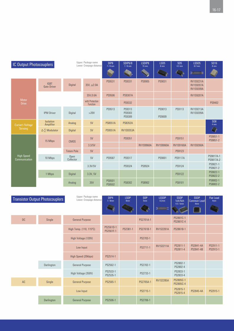
PHOTOCOUPLERS
LSSO5(5pin)/LSSOP(4pin)
¡ Downsizing while maintaining long creepage (35% reduction in mounting area compared to LSO5)
¡ Lineup: IGBT drive, IPM drive, 15 Mbps, Transistor output
Low Input Current 15 Mbps
¡ Suitable for industrial equipment due to the balance of low power,high speed 15 Mbps and high noise rejection
¡ The best package for each application can be selected from various lineup
Providing Highly Reliable, High Accuracy Small Footprint Solutions
Featured Products
Optoelectronics
CMR min. (kV/µs)
Pow
er D
issi
patio
n(m
W)
15
15
Conventional productPS9151
Low power and
High noise rejectionRV1S9160A
New
50
35
Mounting area
Note: Package namePart numberCreepage distance
LSSO5RV1S9260A
8.2mmSO5
RV1S9160A4.2mm
LSO5RV1S9060A
8mm
LSDIP8RV1S9960A
15mm
Isol
atio
n Vo
ltage
(kVr
.m.s
.)
5
3.75
7.5
8.2 mmHalf lead pitch compared to conventional package
0.65 mm
35%
LSO5 LSSO5
Reduction of mounting area
LSO5 LSSO5New
8.0 mm
Industry first package
Reduced area
16-17
DIP47 / 8mm
LSOP8mm
SOP5mm
LSSOP8.2mm
SSOP1ch/4ch4.5 / 5mm
SSOPCommon Lead
4mm
Flat Lead4mm
PS2701A-1PS2801C-1PS2801C-4
PS2561D-1PS2561F-1
PS2381-1 PS2761B-1 RV1S2281A PS2861B-1
PS2703-1
PS2711-1 RV1S2211A
RV1S2285A
PS2811-1PS2811-4
PS2841-4APS2841-4B
PS2911-1PS2913-1
PS2514-1
PS2562-1 PS2702-1PS2802-1PS2802-4
PS2533-1PS2535-1
PS2733-1PS2833-1PS2833-4
PS2565-1 PS2705A-1PS2805C-1PS2805C-4
PS2715-1PS2815-1PS2815-4
PS2845-4A PS2915-1
PS2506-1 PS2706-1
DIP87 / 8 mm
SDIP6/87 / 8 mm
LSDIP815 mm
LSO58 mm
SO54.2 mm
LSSO58.2 mm
SO168 mm
PS9531 PS9331 PS9905 PS9031
PS9506 PS9307A
PS9332 PS9402
PS9513 PS9313PS9303PS9309
PS9013
PS9009
PS9113 RV1S9213ARV1S9209A
RV1S9231ARV1S9207ARV1S9209A
RV1S9207A
PS8551A PS8352A SO84 mm
PS9551A RV1S9353A
PS9351 PS9151
RV1S9160ARV1S9960A RV1S9060A RV1S9260A
PS9851-1PS9851-2
PS9123
PS9587 PS9317 PS9001 PS9117APS9817A-1PS9817A-2
PS9324 PS9924 PS9124PS9821-1PS9821-2
PS9122PS9822-1PS9822-2
PS8802-1PS8802-2
PS8501PS8502
PS8302 PS8902 PS8101
SingleDC
Darlington
SingleAC
Darlington
IsolationAmplifier
IPM Driver
IGBTGate Driver
10 Mbps
1 Mbps
35V, ≥2.0A
5V
5V
>20V
35V,0.6A
5V
5V
3.3/5V
5V
3.3V/5V
3.3V, 5V
35V
Analog
Digital
Digital
Totem Pole
OpenCollector
Digital
Analog
Digital
∆-∑ Modulator
MotorDrive
Current /VoltageSensing
High SpeedCommunication
with ProtectionFunction
General Purpose
High Temp. (110, 115ºC)
High Voltage (120V)
Low Input
High Speed (20kbps)
General Purpose
High Voltage (350V)
General Purpose
Low Input
General Purpose
Transistor Output Photocouplers
IC Output PhotocouplersUpper: Package nameLower: Creepage distance
Upper: Package nameLower: Creepage distance
15 Mbps CMOS
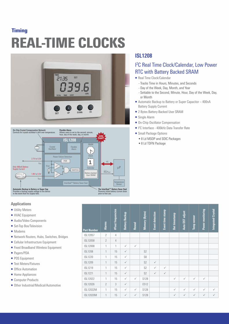
ISL1208
Clock
Calendar
SRAM
POR
SWITCH±
2.7V to 5.5V
1.8V to 5.5V
Only 400nA Battery Supply Current
VTRIP
VDD
VBAT
IRQ/FOUT
I2C
Battery or Super Cap
On-Chip Crystal Compensation Network Corrects for crystal oscillator's drift over temperature.
Automatic Backup to Battery or Super Cap Provides a backup supply voltage to the device in the event that VDD supply fails.
The InterSeal™ Battery Saver Seal Prevents initial battery current drain prior to first use.
Flexible Alarm Allows users to set to the second, minute, hour, day of the week, day, or month.
InterSeal™ Battery Saver Seal
µP
TemperatureSensor
Battery-backed User SRAM
FlexibleAlarm
CrystalOscillator
Power Failure Detection
LowCost!!
REAL-TIME CLOCKSTiming
Applications ¡ Utility Meters
¡ HVAC Equipment
¡ Audio/Video Components
¡ Set-Top Box/Television
¡ Modems
¡ Network Routers, Hubs, Switches, Bridges
¡ Cellular Infrastructure Equipment
¡ Fixed Broadband Wireless Equipment
¡ Pagers/PDA
¡ POS Equipment
¡ Test Meters/Fixtures
¡ Office Automation
¡ Home Appliances
¡ Computer Products
¡ Other Industrial/Medical/Automotive
Part Number Ala
rms
#Fo
ut fr
eque
ncie
s
Bat
tery
Bac
kup
Res
eal
Mem
ory
(Byt
es)
Eve
nt d
etec
tion
Eve
nt ti
me
stam
p
Bat
tim
esta
mp
Aut
o DS
T ad
just
Tem
p se
nsor
Pow
er m
onito
ring
Int
egra
ted
Crys
tal
ISL12057 2 4
ISL12058 2 4
ISL12008 1 1 ü ü
ISL1208 1 15 ü S2
ISL1220 1 15 ü S8
ISL1209 1 15 ü S2 ü
ISL1219 1 15 ü S2 ü ü
ISL1221 1 15 ü S2 ü ü
ISL12022 1 15 ü ü S128 ü ü ü ü
ISL12026 2 3 ü E512
ISL12022M 1 15 ü ü S128 ü ü ü ü ü
ISL12020M 1 15 ü ü S128 ü ü ü ü ü
¡ Real Time Clock/Calendar
- Tracks Time in Hours, Minutes, and Seconds- Day of the Week, Day, Month, and Year- Settable to the Second, Minute, Hour, Day of the Week, Day,
or Month¡ Automatic Backup to Battery or Super Capacitor – 400nA Battery Supply Current
¡ 2 Bytes Battery-Backed User SRAM
¡ Single Alarm
¡ On-Chip Oscillator Compensation
¡ I2C Interface - 400kHz Data Transfer Rate
¡ Small Package Options
• 8 Ld MSOP and SOIC Packages • 8 Ld TDFN Package
ISL1208
I2C Real Time Clock/Calendar, Low Power RTC with Battery Backed SRAM

18-19
HIGH SPEED ADC/DACsData Converters
8-bitSpeed 10-bit 12-bit 14-bit 16-bit
ISLA118P50 ISLA110P50
KAD5510P-50
KAD5510P-25
KAD5610P-25
ISLA112P50 ISLA214P50
ISLA224P25
KAD5514P-25 ISLA216P25
ISLA212P50
KAD5512P-50
ISLA212P25
ISLA222P25
ISLA222S25
KAD5512(H)P-25
KAD5612P-25
KAD5512(H)P-21
KAD5612P-21
ISLA222S20
KAD5512(H)P-17
KAD5510P-21
KAD5610P-21
KAD5510P-12
KAD5610P-12
KAD5512(H)P-12
KAD5512P-12
KAD5514P-12
ISLA224P12
KAD5510P-17
KAD5610P-17
KAD5612P-17
ISLA222P13
KAD5514P-21
ISLA214P20
ISLA224P20
ISLA216P20
ISLA216S20
ISLA216P13
ISLA224S20
KAD5514P-17
Single Dual
500+
250–350
130–210
Up to 125
8-bitDACs 10-bit 12-bit 14-bit
HI5660
ISL5761
ISL5857
ISL5961ISL5861
Single
260MSPS
130–210MSPS
60–125MSPS
Innovative FemtoCharge® CMOS technology yields ultra-high performance ADCs that consume a fraction of the power of the competition.
Competitive Advantages¡ Between half and one fifth the power of the competition
¡ Superior wideband capabilities
¡ Compact footprint
– The industry’s first dual 12-bit 250MSPS ADC
family
– 500 MSPS option is 2 to 3.6x smaller than the
competition
Applications¡ Communications
¡ Networking
¡ Instrumentation
¡ Industrial
¡ Video and imaging
High Speed ADCs
High Speed DACs
Key Features ¡ Excellent dynamic performance (ISL5957)
– Nyquist SFDR at 10MHz = 75dBc
– UMTS ACPR at 19.2MHz = 71dB
¡ GSM SFDR at 11MHz (20MHz window) = 94dBc
¡ +3.3V supply, low power: 103mW @ 130MSPS
¡ Adjustable full-scale output current: 2 to 20mA
¡ Pin compatible family of single and duals
Applications¡ Wireless Comms
¡ Broadband Microwave Repeaters
¡ Military and SDR Radios
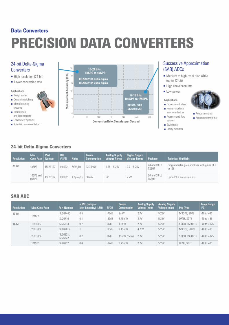
PRECISION DATA CONVERTERSData Converters
12
14
16
18
24
22
20
Mea
sure
men
t Acc
urac
y (b
its)
Conversion Rate, Samples per Second1 10 100 1k 10k 100k 1M
ISL26102/104 Delta-Sigma
ISL2631x SARISL267xx SAR
ISL26132/134 Delta-Sigma
19-24 bits, 1kSPS to 4kSPS
12-18 bits, 10kSPS to 1MSPS
Successive Approximation (SAR) ADCs¡ Medium to high-resolution ADCs (up to 12-bit)
¡ High conversion rate
¡ Low power
24-bit Delta-Sigma Converters¡ High resolution (24-bit)
¡ Lower conversion rate
24-bit Delta-Sigma Converters
SAR ADC
ResolutionMax Conv Rate
Part Number
INL (%FS) Noise
Power Consumption
Analog Supply Voltage Range
Digital Supply Voltage Range Package Technical Highlight
24-bit 4kSPS ISL26102 0.0002 7nV/√Hz 33.75mW 4.75 – 5.25V 2.7 – 5.25V24 and 28 Ld TSSOP
Programmable gain amplifier with gains of 1 to 128
10SPS and 80SPS
ISL26132 0.0002 1.2μV/√Hz 50mW 5V 2.7V24 and 28 Ld TSSOP
Up to 21.6 Noise-free bits
Resolution Max Conv Rate Part Number± INL (Integral Non-Linearity) (LSB) SFDR
Power Consumption
Analog Supply Voltage (min)
Analog Supply Voltage (max) Pkg Type
Temp Range (°C)
10-bit1MSPS
ISL267440 0.5 -76dB 2mW 2.7V 5.25V MSOP8, SOT8 -40 to +85
ISL26710 0.1 -82dB 3.75mW 2.7V 5.25V DFN8, SOT8 -40 to +85
12-bit 125kSPS ISL26313 0.7 96dB 11mW 2.7V 5.25V SOIC8, TSSOP16 -40 to +125
200kSPS ISL267817 1 -85dB 2.15mW 4.75V 5.25V MSOP8, SOIC8 -40 to +85
250kSPSISL26321 , ISL26322
0.7 96dB 11mW, 15mW 2.7V 5.25V SOIC8, TSSOP16 -40 to +125
1MSPS ISL26712 0.4 -87dB 3.75mW 2.7V 5.25V DFN8, SOT8 -40 to +85
Applications
Process controllers
Human-machine interface devices
Pressure and flow sensors
Switchgear
Safety monitors
Robotic controls
Automotive systems
Applications
Weigh scales
Dynamic weighing
Manufacturing systems
Temperature and load sensors
Load safety systems
Scientific instrumentation

20-21
X9C102, X9C103, X9C104, X9C503 Digitally Controlled Potentiometer ¡ Three-Wire Serial Interface
¡ 1kΩ, 10kΩ, 50kΩ, 100kΩ
¡ 100 Wiper Tap Points
• Wiper Position Stored in Non-volatile Memory and Recalled on Power-up
¡ 99 Resistive Elements
• Temperature Compensated
• End-to-End Resistance, ±20%
• Terminal Voltages, ±5V
¡ Low Power CMOS
• VCC = 5V
• Active Current, 3mA max.
• Standby Current, 750µA max. High Reliability
¡ Reliability
• Endurance, 100,000 Data Changes per Bit
• Register Data Retention, 100 years
¡ 8 lead SOIC or PDIP
Nonvolatile
Tap Part Number Resistance kΩ Channels Interface
32 ISL22511 10 1 Pushbutton
X9313 1, 10, 50 1 3-Wire (Up/Down)
X9315 10, 50, 100 1 3-Wire (Up/Down)
X9511 10 1 Pushbutton
64 X9241A 2, 10, 50 1 2-Wire
X9401 10 4 SPI
100 X9317 10, 50 1 3-Wire (Up/Down)
X9318 10 1 3-Wire (Up/Down)
X9C102, 3, 4 1, 10, 100 1 3-Wire(Up/Down)
X9C503 50 1 3-Wire (Up/Down)
128 ISL223x6 10 x = 1, 2, 4 I2C
ISL223x6WM 10 x = 1, 2, 4 I2C
ISL22317 10, 50, 100 1 I2C
ISL95311 10 1 I2C
256 ISL958x0 2.5, 10, 50 x = 1, 2 I2C
X9252 2, 10 4 2-Wire, 3-Wire (Up/Down)
ISL22424 10 2 SPI
X9271, X9251, X9259 50 1, 4 SPI, 2-Wire
X9250, X9258 50, 100 4 SPI , 2-Wire
Other Options with non-Volatile Memory
Tap Part Number Resistance kΩ Channels Interface
32 ISL23511 10 1 Pushbutton
128 ISL23318 10, 100 1 I2C
ISL23418 50 1 SPI
ISL90727, 8 10, 50 1 I2C
ISL23315 10, 100 1 I2C
ISL23328 10 2 I2C
256 ISL23415 10, 100 1 SPI
ISL23325 10, 100 2 I2C
ISL23425 10, 100 2 I2C
ISL90842 10, 50 4 I2C
Other Options with Volatile Memory
DIGITAL POTENTIOMETERS PORTFOLIO
Data Converters
Digital potentiometers replace mechanical potentiometers and trim resistors in applications where digital control allows microprocessor interfacing and extended functionality. Compared to mechanical potentiometers, electronic potentiometers are more accurate, easier to adjust, and they reduce manufacturing complexity. Renesas offers the widest selection of low-to-high resolution digital potentiometers (DCPs) in single, dual and quad configurations that are accurate, easy to adjust and reduce manufacturing complexity.
7-BITUP/DOWNCOUNTER
U/D RH/VH
RL/VL
RW/VW
99
98
97
96
2
1
0
INCCS
GNDVCC
7-BITNON-VOLATILE
MEMORYONEOF
ONE-HUNDREDDECODER
DETAILED
RESISTORARRAY
TRANSFERGATES
STORE ANDRECALL
CONTROLCIRCUITRY
–––
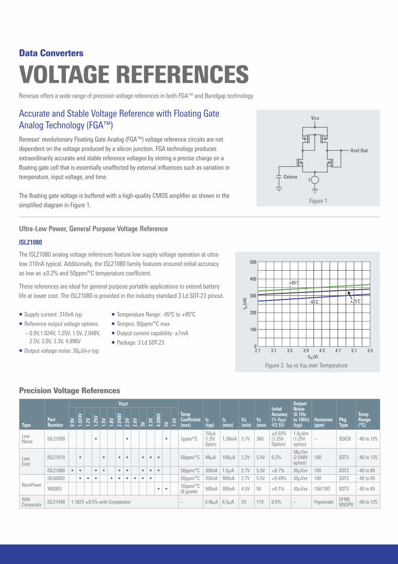
VOLTAGE REFERENCESData Converters
Ultra-Low Power, General Purpose Voltage Reference
ISL21080
The ISL21080 analog voltage references feature low supply voltage operation at ultra-low 310nA typical. Additionally, the ISL21080 family features ensured initial accuracy as low as ±0.2% and 50ppm/°C temperature coefficient.
These references are ideal for general purpose portable applications to extend battery life at lower cost. The ISL21080 is provided in the industry standard 3 Ld SOT-23 pinout.
Renesas offers a wide range of precision voltage references in both FGA™ and Bandgap technology
Accurate and Stable Voltage Reference with Floating Gate Analog Technology (FGA™)Renesas' revolutionary Floating Gate Analog (FGA™) voltage reference circuits are not dependent on the voltage produced by a silicon junction. FGA technology produces extraordinarily accurate and stable reference voltages by storing a precise charge on a floating gate cell that is essentially unaffected by external influences such as variation in temperature, input voltage, and time.
The floating gate voltage is buffered with a high-quality CMOS amplifier as shown in the simplified diagram in Figure 1.
¡ Supply current: 310nA typ
¡ Reference output voltage options:
– 0.9V,1.024V, 1.25V, 1.5V, 2.048V, 2.5V, 3.0V, 3.3V, 4.096V
¡ Output voltage noise: 30μVP-P typ
¡ Temperature Range: -45ºC to +85ºC
¡ Tempco: 50ppm/°C max
¡ Output current capability: ±7mA
¡ Package: 3 Ld SOT-23
Vcc
Cstore
Vref Out
I
500
400+85˚C
-40˚C +25˚C300
200
100
02.7 3.1 3.5 3.9
VIN (V)
I IN (n
A)
4.3 4.7 5.1 5.5
Figure 1
Precision Voltage References
TypePart Number
VOUT
Temp Coefficient (max)
IS (typ)
IS (max)
VS (min)
VS (max)
Initial Accuracy (% VOUT @2.5V)
Output Noise (0.1Hz to 10Hz) (typ)
Hysteresis (ppm)
Pkg Type
Temp Range (°C)0.
9V
1.02
4V
1.2V
1.25
V
1.5V
1.8V
2.04
8V
2.5V
2.6V
3V 3.3V
4.09
6V
5V 7.5V
Low Noise ISL21090 • • • 7ppm/°C
750µA (1.25V Option)
1.28mA 3.7V 36V±0.03% (1.25V Option)
1.0µVPP (1.25V option)
– SOIC8 -40 to 125
Low Cost
ISL21010 • • • • • • • 50ppm/°C 48µA 100µA 2.2V 5.5V 0.2%58µVPP (2.048V option)
100 SOT3 -40 to 125
ISL21080 • • • • • • • • • 50ppm/°C 300nA 1.5µA 2.7V 5.5V <0.7% 30µVPP 100 SOT3 -40 to 85
NanoPowerISL60002 • • • • • • • • • 20ppm/°C 350nA 900nA 2.7V 5.5V <0.49% 30µVPP 100 SOT3 -40 to 85
X60003 • • 10ppm/°C (B grade) 500nA 900nA 4.5V 9V <0.1% 30µVPP 150/100 SOT3 -40 to 85
With Comparator ISL21440 1.182V ±0.5% with Comparator – 0.46µA 6.5µA 2V 11V 0.5% – Programmable DFN8,
MSOP8 -40 to 125
Figure 2. IIN vs VIN over Temperature

22-23
A VOUT
RF1
RF2
RG
VIN
SPST SPDT DPST DPDT MUX 1:n
Out
DecodeLogic
1
2
n
A1 A2 A3
Single, Dual, and Quad Channel Switchesand 4, 8, and 16 Channel Multiplexers
INA
BridgeSensor
ADC MUC
MU
XAdditionalSensor Inputs
ExcitationVoltage
REF
Inverting Amplifier Gain is varied using an Analog Switch Data Acquisition of multiple Sensors using a Multiplexer
ANALOG SWITCHESSwitches & Multiplexers
Renesas' broad portfolio of analog switches and multiplexers (MUX) provide excellent performance across a wide input voltage range. Products include 40V operation down to low voltage USB switching. The following figures and tables only show a fraction of the most commonly preferred analog switches and multiplexers. This portfolio includes single, dual and quad channels of single-pole single-throw and single-pole dual-throw switches, as well as single and dual dual-pole single-throw and dual-pole dual-throw switches, both available in normal-open (NO) and normal-closed (NC) configurations. For selective switching of multiple signal inputs, the input configurations of our multiplexers range from single and dual 4:1 and 8:1 and 16:1.
Data acquisition is the process of sampling signals that measure real-world physical conditions and converting the resulting samples into digital numeric values. Data acquisition circuitry includes sensors that convert physical parameters to electrical signals, signal conditioning circuitry, and analog to digital converters.Data acquisition applications require analog switch and multiplexer products with low charge injection and parasitic capacitance to minimize switching errors and settling time in the input multiplexer and sample and hold circuits. Renesas offers high performance for these parameters, enabling high sampling rates and accuracy. In addition, Renesas also offers switches with low on-resistance that are suitable for mode switch, filtering, and programmable gain control applications.
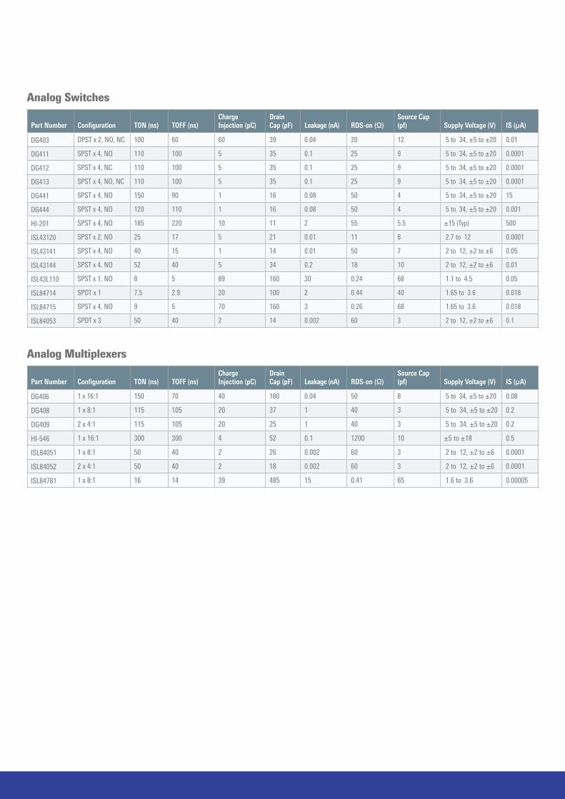
Analog Switches
Analog Multiplexers
Part Number Configuration TON (ns) TOFF (ns)Charge Injection (pC)
Drain Cap (pF) Leakage (nA) RDS-on (Ω)
Source Cap (pf) Supply Voltage (V) IS (µA)
DG406 1 x 16:1 150 70 40 180 0.04 50 8 5 to 34, ±5 to ±20 0.08
DG408 1 x 8:1 115 105 20 37 1 40 3 5 to 34, ±5 to ±20 0.2
DG409 2 x 4:1 115 105 20 25 1 40 3 5 to 34, ±5 to ±20 0.2
HI-546 1 x 16:1 300 300 4 52 0.1 1200 10 ±5 to ±18 0.5
ISL84051 1 x 8:1 50 40 2 26 0.002 60 3 2 to 12, ±2 to ±6 0.0001
ISL84052 2 x 4:1 50 40 2 18 0.002 60 3 2 to 12, ±2 to ±6 0.0001
ISL84781 1 x 8:1 16 14 39 485 15 0.41 65 1.6 to 3.6 0.00005
Part Number Configuration TON (ns) TOFF (ns)Charge Injection (pC)
Drain Cap (pF) Leakage (nA) RDS-on (Ω)
Source Cap (pf) Supply Voltage (V) IS (µA)
DG403 DPST x 2, NO, NC 100 60 60 39 0.04 20 12 5 to 34, ±5 to ±20 0.01
DG411 SPST x 4, NO 110 100 5 35 0.1 25 9 5 to 34, ±5 to ±20 0.0001
DG412 SPST x 4, NC 110 100 5 35 0.1 25 9 5 to 34, ±5 to ±20 0.0001
DG413 SPST x 4, NO, NC 110 100 5 35 0.1 25 9 5 to 34, ±5 to ±20 0.0001
DG441 SPST x 4, NO 150 90 1 16 0.08 50 4 5 to 34, ±5 to ±20 15
DG444 SPST x 4, NO 120 110 1 16 0.08 50 4 5 to 34, ±5 to ±20 0.001
HI-201 SPST x 4, NO 185 220 10 11 2 55 5.5 ±15 (Typ) 500
ISL43120 SPST x 2, NO 25 17 5 21 0.01 11 8 2.7 to 12 0.0001
ISL43141 SPST x 4, NO 40 15 1 14 0.01 50 7 2 to 12, ±2 to ±6 0.05
ISL43144 SPST x 4, NO 52 40 5 34 0.2 18 10 2 to 12, ±2 to ±6 0.01
ISL43L110 SPST x 1, NO 8 5 89 160 30 0.24 68 1.1 to 4.5 0.05
ISL84714 SPDT x 1 7.5 2.9 20 100 2 0.44 40 1.65 to 3.6 0.018
ISL84715 SPST x 4, NO 9 5 70 160 3 0.26 68 1.65 to 3.6 0.018
ISL84053 SPDT x 3 50 40 2 14 0.002 60 3 2 to 12, ±2 to ±6 0.1

24-25
MEMO
www.renesas.com
Notice1. Descriptions of circuits, software and other related information in this document are provided only to illustrate the operation of semiconductor products and application examples. You are fully responsible for the incorporation or any other use of the circuits, software, and information in the
design of your product or system. Renesas Electronics disclaims any and all liability for any losses and damages incurred by you or third parties arising from the use of these circuits, software, or information.2. Renesas Electronics hereby expressly disclaims any warranties against and liability for infringement or any other claims involving patents, copyrights, or other intellectual property rights of third parties, by or arising from the use of Renesas Electronics products or technical information described
in this document, including but not limited to, the product data, drawings, charts, programs, algorithms, and application examples.3. No license, express, implied or otherwise, is granted hereby under any patents, copyrights or other intellectual property rights of Renesas Electronics or others.4. You shall be responsible for determining what licenses are required from any third parties, and obtaining such licenses for the lawful import, export, manufacture, sales, utilization, distribution or other disposal of any products incorporating Renesas Electronics products, if required.5. You shall not alter, modify, copy, or reverse engineer any Renesas Electronics product, whether in whole or in part. Renesas Electronics disclaims any and all liability for any losses or damages incurred by you or third parties arising from such alteration, modification, copying or reverse
engineering.6. Renesas Electronics products are classified according to the following two quality grades: “Standard” and “High Quality”. The intended applications for each Renesas Electronics product depends on the product’s quality grade, as indicated below. "Standard": Computers; office equipment; communications equipment; test and measurement equipment; audio and visual equipment; home electronic appliances; machine tools; personal electronic equipment; industrial robots; etc. "High Quality": Transportation equipment (automobiles, trains, ships, etc.); traffic control (traffic lights); large-scale communication equipment; key financial terminal systems; safety control equipment; etc. Unless expressly designated as a high reliability product or a product for harsh environments in a Renesas Electronics data sheet or other Renesas Electronics document, Renesas Electronics products are not intended or authorized for use in products or systems that may pose a direct threat to
human life or bodily injury (artificial life support devices or systems; surgical implantations; etc.), or may cause serious property damage (space system; undersea repeaters; nuclear power control systems; aircraft control systems; key plant systems; military equipment; etc.). Renesas Electronics disclaims any and all liability for any damages or losses incurred by you or any third parties arising from the use of any Renesas Electronics product that is inconsistent with any Renesas Electronics data sheet, user’s manual or other Renesas Electronics document.
7. No semiconductor product is absolutely secure. Notwithstanding any security measures or features that may be implemented in Renesas Electronics hardware or software products, Renesas Electronics shall have absolutely no liability arising out of any vulnerability or security breach, including but not limited to any unauthorized access to or use of a Renesas Electronics product or a system that uses a Renesas Electronics product. RENESAS ELECTRONICS DOES NOT WARRANT OR GUARANTEE THAT RENESAS ELECTRONICS PRODUCTS, OR ANY SYSTEMS CREATED USING RENESAS ELECTRONICS PRODUCTS WILL BE INVULNERABLE OR FREE FROM CORRUPTION, ATTACK, VIRUSES, INTERFERENCE, HACKING, DATA LOSS OR THEFT, OR OTHER SECURITY INTRUSION (“Vulnerability Issues”). RENESAS ELECTRONICS DISCLAIMS ANY AND ALL RESPONSIBILITY OR LIABILITY ARISING FROM OR RELATED TO ANY VULNERABILITY ISSUES. FURTHERMORE, TO THE EXTENT PERMITTED BY APPLICABLE LAW, RENESAS ELECTRONICS DISCLAIMS ANY AND ALL WARRANTIES, EXPRESS OR IMPLIED, WITH RESPECT TO THIS DOCUMENT AND ANY RELATED OR ACCOMPANYING SOFTWARE OR HARDWARE, INCLUDING BUT NOT LIMITED TO THE IMPLIED WARRANTIES OF MERCHANTABILITY, OR FITNESS FOR A PARTICULAR PURPOSE.
8. When using Renesas Electronics products, refer to the latest product information (data sheets, user’s manuals, application notes, “General Notes for Handling and Using Semiconductor Devices” in the reliability handbook, etc.), and ensure that usage conditions are within the ranges specified by Renesas Electronics with respect to maximum ratings, operating power supply voltage range, heat dissipation characteristics, installation, etc. Renesas Electronics disclaims any and all liability for any malfunctions, failure or accident arising out of the use of Renesas Electronics products outside of such specified ranges.
9. Although Renesas Electronics endeavors to improve the quality and reliability of Renesas Electronics products, semiconductor products have specific characteristics, such as the occurrence of failure at a certain rate and malfunctions under certain use conditions. Unless designated as a high reliability product or a product for harsh environments in a Renesas Electronics data sheet or other Renesas Electronics document, Renesas Electronics products are not subject to radiation resistance design. You are responsible for implementing safety measures to guard against the possibility of bodily injury, injury or damage caused by fire, and/or danger to the public in the event of a failure or malfunction of Renesas Electronics products, such as safety design for hardware and software, including but not limited to redundancy, fire control and malfunction prevention, appropriate treatment for aging degradation or any other appropriate measures. Because the evaluation of microcomputer software alone is very difficult and impractical, you are responsible for evaluating the safety of the final products or systems manufactured by you.
10. Please contact a Renesas Electronics sales office for details as to environmental matters such as the environmental compatibility of each Renesas Electronics product. You are responsible for carefully and sufficiently investigating applicable laws and regulations that regulate the inclusion or use of controlled substances, including without limitation, the EU RoHS Directive, and using Renesas Electronics products in compliance with all these applicable laws and regulations. Renesas Electronics disclaims any and all liability for damages or losses occurring as a result of your noncompliance with applicable laws and regulations.
11. Renesas Electronics products and technologies shall not be used for or incorporated into any products or systems whose manufacture, use, or sale is prohibited under any applicable domestic or foreign laws or regulations. You shall comply with any applicable export control laws and regulations promulgated and administered by the governments of any countries asserting jurisdiction over the parties or transactions.
12. It is the responsibility of the buyer or distributor of Renesas Electronics products, or any other party who distributes, disposes of, or otherwise sells or transfers the product to a third party, to notify such third party in advance of the contents and conditions set forth in this document.13. This document shall not be reprinted, reproduced or duplicated in any form, in whole or in part, without prior written consent of Renesas Electronics.14. Please contact a Renesas Electronics sales office if you have any questions regarding the information contained in this document or Renesas Electronics products.(Note 1) “Renesas Electronics” as used in this document means Renesas Electronics Corporation and also includes its directly or indirectly controlled subsidiaries.(Note 2) “Renesas Electronics product(s)” means any product developed or manufactured by or for Renesas Electronics.
SALES OFFICESRefer to "http://www.renesas.com/" for the latest and detailed information.
Renesas Electronics CorporationTOYOSU FORESIA, 3-2-24 Toyosu, Koto-ku, Tokyo 135-0061, Japan
Renesas Electronics America Inc. Milpitas Campus1001 Murphy Ranch Road, Milpitas, CA 95035, U.S.A.Tel: +1-408-432-8888, Fax: +1-408-434-5351
Renesas Electronics America Inc. San Jose Campus6024 Silver Creek Valley Road, San Jose, CA 95138, USATel: +1-408-284-8200, Fax: +1-408-284-2775
Renesas Electronics Canada Limited9251 Yonge Street, Suite 8309 Richmond Hill, Ontario Canada L4C 9T3Tel: +1-905-237-2004
Renesas Electronics Europe GmbHArcadiastrasse 10, 40472 Düsseldorf, GermanyTel: +49-211-6503-0, Fax: +49-211-6503-1327
Renesas Electronics (China) Co., Ltd.Room 101-T01, Floor 1, Building 7, Yard No. 7, 8th Street, Shangdi, Haidian District, Beijing 100085, ChinaTel: +86-10-8235-1155, Fax: +86-10-8235-7679
Renesas Electronics (Shanghai) Co., Ltd.Unit 301, Tower A, Central Towers, 555 Langao Road, Putuo District, Shanghai 200333, ChinaTel: +86-21-2226-0888, Fax: +86-21-2226-0999
Renesas Electronics Hong Kong LimitedUnit 1601-1611, 16/F., Tower 2, Grand Century Place, 193 Prince Edward Road West, Mongkok, Kowloon, Hong KongTel: +852-2265-6688, Fax: +852 2886-9022
Renesas Electronics Taiwan Co., Ltd.13F, No. 363, Fu Shing North Road, Taipei 10543, TaiwanTel: +886-2-8175-9600, Fax: +886 2-8175-9670
Renesas Electronics Singapore Pte. Ltd.80 Bendemeer Road, #06-02 Singapore 339949Tel: +65-6213-0200, Fax: +65-6213-0300
Renesas Electronics Malaysia Sdn.Bhd.Unit No 3A-1 Level 3A Tower 8 UOA Business Park, No 1 Jalan Pengaturcara U1/51A, Seksyen U1, 40150 Shah Alam, Selangor, MalaysiaTel: +60-3-5022-1288, Fax: +60-3-5022-1290
Renesas Electronics India Pvt. Ltd.No.777C, 100 Feet Road, HAL 2nd Stage, Indiranagar, Bangalore 560 038, IndiaTel: +91-80-67208700
Renesas Electronics Korea Co., Ltd.17F, KAMCO Yangjae Tower, 262, Gangnam-daero, Gangnam-gu, Seoul, 06265 KoreaTel: +82-2-558-3737, Fax: +82-2-558-5338
(Rev.5.0-1 October 2020)
© 2021 Renesas Electronics Corporation.All rights reserved.
Document No. R07CL0009EJ0400


![· Transducer Interfacing Handbook. ... Dan Sheingold [dan.sheingold@analog.com] ANALOG ICs POWER DIGITAL TVs At midnight on February 17, 2009, most commercial analog TV broadcasts—long](https://img.pdfslide.us/doc/110x75/5c8e7ab609d3f270788d041e/-transducer-interfacing-handbook-dan-sheingold-dansheingold-analog.jpg)