Embed Size (px)
Citation preview
Available online at www.sciencedirect.com
www.elsevier.com/locate/actamat
ScienceDirect
Acta Materialia 63 (2014) 191–201
Relation between thermolectric properties and phase equilibriain the ZnO–In2O3 binary system
Xin Liang ⇑, David R. Clarke
School of Engineering and Applied Sciences, Harvard University, Cambridge, MA 02138, USA
Received 24 July 2013; accepted 15 October 2013Available online 9 November 2013
Abstract
The electrical conductivities, Seebeck coefficients and thermal conductivities across the ZnO–In2O3 binary system are reported andrelated to the phase compositions and microstructures present at 1150 and 1250 �C. The ZnO–In2O3 binary system is of particular inter-est as it contains a variety of different types of phases, superlattice (modular) phases, solid solutions, two-phase regions and crystallo-graphic features. Throughout much of the phase diagram, the thermal conductivities are less than 2 W m�1 K�1, being limited by bothsolid solution disorder and thermal resistance due to the presence of InO/ZnO interfaces. Across the phase diagram, irrespective of theactual phases, the materials behave at high temperatures (800 �C) as free-electron conductors with the Seebeck coefficient and electronconductivity satisfying the Jonker’s relationship. In the two-phase regions of the phase diagram, the values of the power factor and figureof merit (ZT) are consistent with a simple law of mixtures, weighted according to the volume fractions of the two phases. Although thelargest values of electrical conductivity and Seebeck coefficient occur over a range of composition centered at 40 m/o InO1.5, the max-imum ZT and power factors are observed at k = 4 (33 m/o InO1.5). In contrast to the other modular phases at 1250 �C and below, thisphase is hexagonal rather than rhombohedral.Published by Elsevier Ltd. on behalf of Acta Materialia Inc.
Keywords: Thermoelectrics; Oxide; Microstructure; Superlattice; Two-phase materials
1. Introduction
Studies of the thermoelectric properties of materials areusually restricted to a single composition or compound ofinterest and report on the effect of variables, such as dop-ing concentration [1–8], processing or grain size [9]. Whilesuch studies are essential once a promising material hasbeen identified and provide invaluable information, theydo not include the effect of compositional changes withthe exception of simple solid solutions, for instance sili-con–germanium [10]. In contrast, in this work we investi-gate the thermoelectric properties over the fullcompositional range of the ZnO–In2O3 binary system inorder to explore systematic variations with composition.
1359-6454/$36.00 Published by Elsevier Ltd. on behalf of Acta Materialia Inc
http://dx.doi.org/10.1016/j.actamat.2013.10.027
⇑ Corresponding author. Tel.: +1 617 496 4295.E-mail address: [email protected] (X. Liang).
This oxide material system is of interest as the basis forhigh-temperature thermoelectrics [11–15] and because itexhibits a range of possible phases and microstructures[16]. These range from the pure compounds, simple solidsolutions, two-phase regions and modular or naturalsuperlattice (SL) compounds [17], as well as solid solutionphases containing planar interfaces. This unusual varietyprovides an opportunity to quantify the effects of pointdefect scattering and interface scattering as well as phasecontent on the thermal and electrical conductivity, allwithin the same system. Investigation of the two-phasecompositions also enables us to compare with the mean-field predictions of the thermoelectric properties of two-phase polycrystalline materials.
The thermal-to-electrical efficiency of thermoelectrics, g,is usually given in terms of a non-dimensional figure ofmerit, ZT:
.
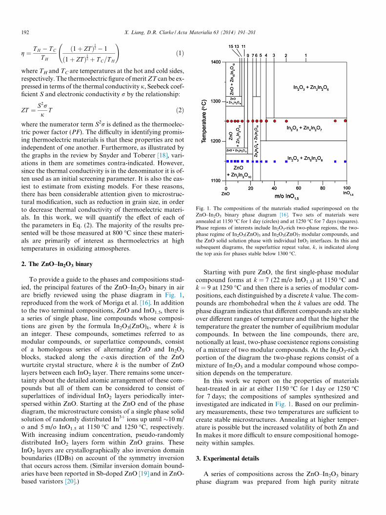
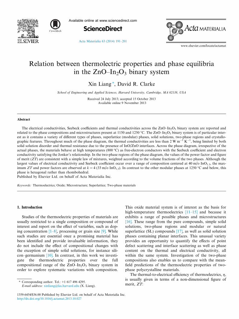
Fig. 1. The compositions of the materials studied superimposed on theZnO–In2O3 binary phase diagram [16]. Two sets of materials wereannealed at 1150 �C for 1 day (circles) and at 1250 �C for 7 days (squares).Phase regions of interests include In2O3-rich two-phase regions, the two-phase regime of In2O3(ZnO)5 and In2O3(ZnO)7 modular compounds, andthe ZnO solid solution phase with individual InO2 interfaces. In this andsubsequent diagrams, the superlattice repeat value, k, is indicated alongthe top axis for phases stable below 1300 �C.
192 X. Liang, D.R. Clarke / Acta Materialia 63 (2014) 191–201
g ¼ T H � T C
T H
ð1þ ZT Þ12 � 1
ð1þ ZT Þ12 þ T C=T H
!ð1Þ
where TH and TC are temperatures at the hot and cold sides,respectively. The thermoelectric figure of merit ZT can be ex-pressed in terms of the thermal conductivity j, Seebeck coef-ficient S and electronic conductivity r by the relationship:
ZT ¼ S2rj
T ð2Þ
where the numerator term S2r is defined as the thermoelec-tric power factor (PF). The difficulty in identifying promis-ing thermoelectric materials is that these properties are notindependent of one another. Furthermore, as illustrated bythe graphs in the review by Snyder and Toberer [18], vari-ations in them are sometimes contra-indicated. However,since the thermal conductivity is in the denominator it is of-ten used as an initial screening parameter. It is also the eas-iest to estimate from existing models. For these reasons,there has been considerable attention given to microstruc-tural modification, such as reduction in grain size, in orderto decrease thermal conductivity of thermoelectric materi-als. In this work, we will quantify the effect of each ofthe parameters in Eq. (2). The majority of the results pre-sented will be those measured at 800 �C since these materi-als are primarily of interest as thermoelectrics at hightemperatures in oxidizing atmospheres.
2. The ZnO–In2O3 binary
To provide a guide to the phases and compositions stud-ied, the principal features of the ZnO–In2O3 binary in airare briefly reviewed using the phase diagram in Fig. 1,reproduced from the work of Moriga et al. [16]. In additionto the two terminal compositions, ZnO and InO1.5, there isa series of single phase, line compounds whose composi-tions are given by the formula In2O3(ZnO)k, where k isan integer. These compounds, sometimes referred to asmodular compounds, or superlattice compounds, consistof a homologous series of alternating ZnO and In2O3
blocks, stacked along the c-axis direction of the ZnOwurtzite crystal structure, where k is the number of ZnOlayers between each InO2 layer. There remains some uncer-tainty about the detailed atomic arrangement of these com-pounds but all of them can be considered to consist ofsuperlattices of individual InO2 layers periodically inter-spersed within ZnO. Starting at the ZnO end of the phasediagram, the microstructure consists of a single phase solidsolution of randomly distributed In3+ ions up until �10 m/o and 5 m/o InO1.5 at 1150 �C and 1250 �C, respectively.With increasing indium concentration, pseudo-randomlydistributed InO2 layers form within ZnO grains. TheseInO2 layers are crystallographically also inversion domainboundaries (IDBs) on account of the symmetry inversionthat occurs across them. (Similar inversion domain bound-aries have been reported in Sb-doped ZnO [19] and in ZnO-based varistors [20].)
Starting with pure ZnO, the first single-phase modularcompound forms at k = 7 (22 m/o InO1.5) at 1150 �C andk = 9 at 1250 �C and then there is a series of modular com-positions, each distinguished by a discrete k value. The com-pounds are rhombohedral when the k values are odd. Thephase diagram indicates that different compounds are stableover different ranges of temperature and that the higher thetemperature the greater the number of equilibrium modularcompounds. In between the line compounds, there are,notionally at least, two-phase coexistence regions consistingof a mixture of two modular compounds. At the In2O3-richportion of the diagram the two-phase regions consist of amixture of In2O3 and a modular compound whose compo-sition depends on the temperature.
In this work we report on the properties of materialsheat-treated in air at either 1150 �C for 1 day or 1250 �Cfor 7 days; the compositions of samples synthesized andinvestigated are indicated in Fig. 1. Based on our prelimin-ary measurements, these two temperatures are sufficient tocreate stable microstructures. Annealing at higher temper-ature is possible but the increased volatility of both Zn andIn makes it more difficult to ensure compositional homoge-neity within samples.
3. Experimental details
A series of compositions across the ZnO–In2O3 binaryphase diagram was prepared from high purity nitrate
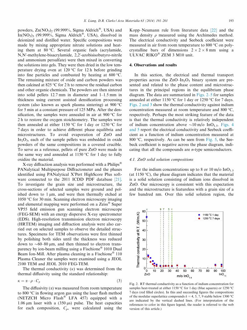
Fig. 2. RT thermal conductivity as a function of indium concentration forsamples heat-treated at either 1150 �C for 1 day (blue squares) or 1250 �C7 days (red filled circles). In this and succeeding figures the compositionsof the modular superlattice compounds k = 4, 5, 7, 9 stable below 1300 �Care indicated by the vertical dashed lines. (For interpretation of thereferences to color in this figure legend, the reader is referred to the webversion of this article.)
X. Liang, D.R. Clarke / Acta Materialia 63 (2014) 191–201 193
powders, Zn(NO3)2 (99.999%, Sigma Aldrich�, USA) andIn(NO3)3 (99.999%, Sigma Aldrich�, USA), dissolved indeionized and distilled water. Specific compositions weremade by mixing appropriate nitrate solutions and heat-ing them at 80 �C. Several organic fuels (acrylamide,N,N0-methylene-bisacrylamide, 2,20-azobisisobutyro-nitrileand ammonium persulfate) were then mixed in convertingthe solutions into gels. They were then dried in the low tem-perature drying oven at 120 �C for 12 h before grindinginto fine particles and combusted by heating at 600 �C.The remaining mixture of oxide and carbon powders wasthen calcined at 825 �C for 2 h to remove the residual carbonand other organic chemicals. The powders are then sinteredinto solid pellets 12.7 mm in diameter and 1–1.5 mm inthickness using current assisted densification processingsystem (also known as spark plasma sintering) at 900 �Cfor 5 min at a constant pressure of 125 MPa. After the den-sification, the samples were annealed in air at 900 �C for2 h to restore the oxygen stoichiometry. The samples werethen annealed at either 1150 �C for 1 day or 1250 �C for7 days in order to achieve different phase equilibria andmicrostructures. To avoid evaporation of ZnO andIn2O3, each of the sample pellets was embedded in oxidepowders of the same compositions in a covered crucible.To serve as a reference, pellets of pure ZnO were made inthe same way and annealed at 1150 �C for 1 day to fullyoxidize the material.
X-ray diffraction analysis was performed with a Philips�
PANalytical Multipurpose Diffractometer and the phasesidentified using PANalytical X’Pert HighScore Plus soft-ware connected to the 2011 ICDD PDF database [21].To investigate the grain size and microstructure, thecross-sections of selected samples were ground and pol-ished down to 1 lm, and were then thermally etched at1050 �C for 30 min. Scanning electron microscopy imagingand elemental mapping were performed on a Zeiss� SuperVP55 field emission gun scanning electron microscope(FEG-SEM) with an energy dispersive X-ray spectrometer(EDS). High-resolution transmission electron microscopy(HRTEM) imaging and diffraction analysis were also car-ried out on selected samples to observe the detailed struc-tures. Specimens for TEM observations were first thinnedby polishing both sides until the thickness was reduceddown to �60–80 lm, and then thinned to electron trans-parency by ion-beam milling using a Fischione� 1010 DualBeam Ion-Mill. After plasma cleaning in a Fischione� 110Plasma Cleaner the samples were examined using a JEOL2100 TEM and JEOL 2010 FEG-TEM.
The thermal conductivity (j) was determined from thethermal diffusivity using the standard relationship:
j ¼ a � q � Cp ð3ÞThe diffusivity (a) was measured from room temperature
to 800 �C in flowing argon gas using the laser flash method(NETZCH Micro Flash� LFA 457) equipped with a1.06 lm laser with a (350 ls) pulse. The heat capacitiesfor each composition, Cp, were calculated using the
Kopp–Neumann rule from literature data [22] and themass density q measured using the Archimedes method.The electrical conductivity and Seebeck coefficient weremeasured in air from room temperature to 800 �C on poly-crystalline bars of dimensions 2 � 2 � 8 mm using aULVAC RIKO� ZEM 3 M10 unit.
4. Observations and results
In this section, the electrical and thermal transportproperties across the ZnO–In2O3 binary system are pre-sented and related to the phase content and microstruc-tures in the principal regions in the equilibrium phasediagram. The data are summarized in Figs. 2–5 for samplesannealed at either 1150 �C for 1 day or 1250 �C for 7 days.Figs. 2 and 3 show the thermal conductivity against indiumconcentration measured at room temperature and 800 �C,respectively. Perhaps the most striking feature of the datais that the thermal conductivity is relatively independentof indium concentration above �10 m/o InO1.5. Figs. 4and 5 report the electrical conductivity and Seebeck coeffi-cient as a function of indium concentration measured at800 �C, respectively. As can be seen from Fig. 5, the See-beck coefficient is negative across the phase diagram, indi-cating that all the compounds are n-type semiconductors.
4.1. ZnO solid solution compositions
For the indium concentrations up to 8 or 10 m/o InO1.5
(at 1150 �C), the phase diagram indicates that the materialis a solid solution consisting of indium ions dissolved inZnO. Our microscopy is consistent with this expectationand the microstructure is featureless with a grain size of afew hundred nm. Over this solid solution region, the
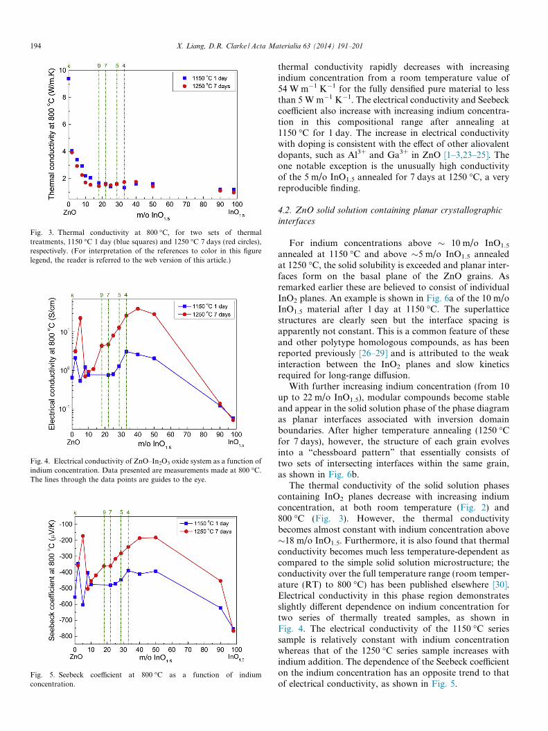
Fig. 3. Thermal conductivity at 800 �C, for two sets of thermaltreatments, 1150 �C 1 day (blue squares) and 1250 �C 7 days (red circles),respectively. (For interpretation of the references to color in this figurelegend, the reader is referred to the web version of this article.)
Fig. 4. Electrical conductivity of ZnO–In2O3 oxide system as a function ofindium concentration. Data presented are measurements made at 800 �C.The lines through the data points are guides to the eye.
Fig. 5. Seebeck coefficient at 800 �C as a function of indiumconcentration.
194 X. Liang, D.R. Clarke / Acta Materialia 63 (2014) 191–201
thermal conductivity rapidly decreases with increasingindium concentration from a room temperature value of54 W m�1 K�1 for the fully densified pure material to lessthan 5 W m�1 K�1. The electrical conductivity and Seebeckcoefficient also increase with increasing indium concentra-tion in this compositional range after annealing at1150 �C for 1 day. The increase in electrical conductivitywith doping is consistent with the effect of other aliovalentdopants, such as Al3+ and Ga3+ in ZnO [1–3,23–25]. Theone notable exception is the unusually high conductivityof the 5 m/o InO1.5 annealed for 7 days at 1250 �C, a veryreproducible finding.
4.2. ZnO solid solution containing planar crystallographicinterfaces
For indium concentrations above � 10 m/o InO1.5
annealed at 1150 �C and above �5 m/o InO1.5 annealedat 1250 �C, the solid solubility is exceeded and planar inter-faces form on the basal plane of the ZnO grains. Asremarked earlier these are believed to consist of individualInO2 planes. An example is shown in Fig. 6a of the 10 m/oInO1.5 material after 1 day at 1150 �C. The superlatticestructures are clearly seen but the interface spacing isapparently not constant. This is a common feature of theseand other polytype homologous compounds, as has beenreported previously [26–29] and is attributed to the weakinteraction between the InO2 planes and slow kineticsrequired for long-range diffusion.
With further increasing indium concentration (from 10up to 22 m/o InO1.5), modular compounds become stableand appear in the solid solution phase of the phase diagramas planar interfaces associated with inversion domainboundaries. After higher temperature annealing (1250 �Cfor 7 days), however, the structure of each grain evolvesinto a “chessboard pattern” that essentially consists oftwo sets of intersecting interfaces within the same grain,as shown in Fig. 6b.
The thermal conductivity of the solid solution phasescontaining InO2 planes decrease with increasing indiumconcentration, at both room temperature (Fig. 2) and800 �C (Fig. 3). However, the thermal conductivitybecomes almost constant with indium concentration above�18 m/o InO1.5. Furthermore, it is also found that thermalconductivity becomes much less temperature-dependent ascompared to the simple solid solution microstructure; theconductivity over the full temperature range (room temper-ature (RT) to 800 �C) has been published elsewhere [30].Electrical conductivity in this phase region demonstratesslightly different dependence on indium concentration fortwo series of thermally treated samples, as shown inFig. 4. The electrical conductivity of the 1150 �C seriessample is relatively constant with indium concentrationwhereas that of the 1250 �C series sample increases withindium addition. The dependence of the Seebeck coefficienton the indium concentration has an opposite trend to thatof electrical conductivity, as shown in Fig. 5.
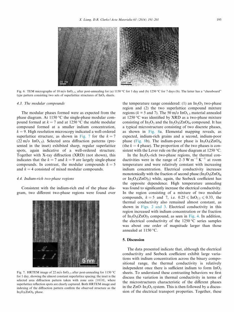
Fig. 6. TEM micrographs of 10 m/o InO1.5, after post-annealing for (a) 1150 �C for 1 day and (b) 1250 �C for 7 days (b). The latter has a “chessboard”
type pattern consisting two sets of superlattice structures of InO2 sheets.
X. Liang, D.R. Clarke / Acta Materialia 63 (2014) 191–201 195
4.3. The modular compounds
The modular phases formed were as expected from thephase diagram. At 1150 �C the single-phase modular com-pound formed at k = 7 and at 1250 �C the stable modularcompound formed at a smaller indium concentration,k = 9. High resolution microscopy indicated a well-orderedsuperlattice structure, as shown in Fig. 7 for the k = 7(22 m/o InO1.5). Selected area diffraction patterns (pre-sented in the inset) exhibited sharp, regular superlatticespots, again indicative of a well-ordered structure.Together with X-ray diffraction (XRD) (not shown), thisindicates that the k = 7 and k = 9 are largely single-phasecompounds. In contrast, the modular compounds k = 5and k = 4 consisted of mixed modular compounds.
4.4. Indium-rich two-phase regions
Consistent with the indium-rich end of the phase dia-gram, two different two-phase regions were found over
Fig. 7. HRTEM image of 22 m/o InO1.5 after post-annealing for 1150 �Cfor 1 day, showing the almost constant superlattice spacing; the inset is theselected area diffraction pattern taken with zone axis h10�10i, wheresuperlattice reflection spots are clearly captured. Both HRTEM image andindexing of the diffraction pattern confirm the observed structure as theIn2O3(ZnO)k phase.
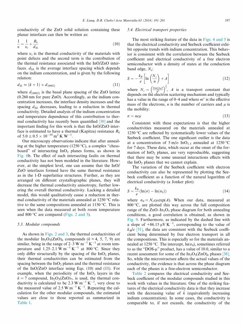
the temperature range considered: (1) an In2O3 two-phaseregion and (2) the two superlattice compound mixtureregions (k = 5 and 7). The 50 m/o InO1.5 material annealedat 1250 �C was identified by XRD as a two-phase mixtureconsisting of In2O3 and the In2O3(ZnO)4 compound. It hasa typical microstructure consisting of two discrete phases,as shown in Fig. 8a. Elemental mapping reveals, asexpected, indium-rich grains and a second, indium-poorphase (Fig. 8b). The indium-poor phase is In2O3(ZnO)4
(the k = 4 phase). The proportion of the two phases is con-sistent with the Lever rule on the phase diagram at 1250 �C.
In the In2O3-rich two-phase regions, the thermal con-ductivities were in the range of 2–3 W m�1 K�1 at roomtemperature and were relatively constant with increasingindium concentration. Electrical conductivity increasesmonotonically with the fraction of second phase (In2O3(ZnO)4
or In2O3(ZnO)5) while, again, the Seebeck coefficient hasthe opposite dependence. High temperature annealingwas found to significantly increase the electrical conductivity.In the region consisting of a mixture of two modularcompounds, k = 5 and 7, i.e. 0:25 6 InO1:5 6 0:33, thethermal conductivity also remained almost constant, asshown in Figs. 2 and 3. Electrical conductivity in thisregion increased with indium concentration or the fractionof In2O3(ZnO)5 compound, as seen in Fig. 4. In addition,the electrical conductivity of the 1250 �C series sampleswas about one order of magnitude larger than thoseannealed at 1150 �C.
5. Discussion
The data presented indicate that, although the electricalconductivity and Seebeck coefficient exhibit large varia-tions with indium concentration across the binary compo-sitional range, the thermal conductivity is relativelyindependent once there is sufficient indium to form InO2
sheets. To understand these contrasting behaviors we firstdiscuss the variation in thermal conductivity in terms ofthe microstructures characteristic of the different phasesin the ZnO–In2O3 system. This is then followed by a discus-sion of the electrical transport properties. Together, these
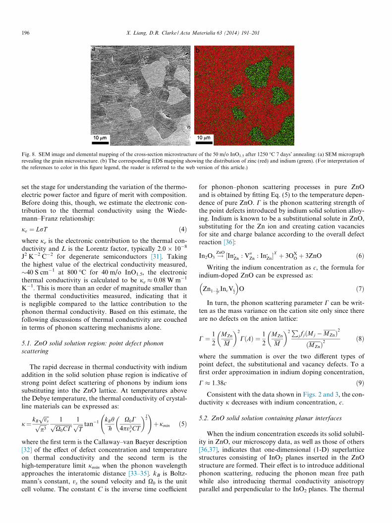
Fig. 8. SEM image and elemental mapping of the cross-section microstructure of the 50 m/o InO1.5 after 1250 �C 7 days’ annealing: (a) SEM micrographrevealing the grain microstructure. (b) The corresponding EDS mapping showing the distribution of zinc (red) and indium (green). (For interpretation ofthe references to color in this figure legend, the reader is referred to the web version of this article.)
196 X. Liang, D.R. Clarke / Acta Materialia 63 (2014) 191–201
set the stage for understanding the variation of the thermo-electric power factor and figure of merit with composition.Before doing this, though, we estimate the electronic con-tribution to the thermal conductivity using the Wiede-mann–Franz relationship:
je ¼ LrT ð4Þwhere je is the electronic contribution to the thermal con-ductivity and L is the Lorentz factor, typically 2.0 � 10�8
J2 K�2 C�2 for degenerate semiconductors [31]. Takingthe highest value of the electrical conductivity measured,�40 S cm�1 at 800 �C for 40 m/o InO1.5, the electronicthermal conductivity is calculated to be je � 0.08 W m�1
K�1. This is more than an order of magnitude smaller thanthe thermal conductivities measured, indicating that itis negligible compared to the lattice contribution to thephonon thermal conductivity. Based on this estimate, thefollowing discussions of thermal conductivity are couchedin terms of phonon scattering mechanisms alone.
5.1. ZnO solid solution region: point defect phonon
scattering
The rapid decrease in thermal conductivity with indiumaddition in the solid solution phase region is indicative ofstrong point defect scattering of phonons by indium ionssubstituting into the ZnO lattice. At temperatures abovethe Debye temperature, the thermal conductivity of crystal-line materials can be expressed as:
j¼ kBffiffiffiffivspffiffiffiffiffip3p 1ffiffiffiffiffiffiffiffiffiffiffiffi
X0CCp 1ffiffiffiffi
Tp tan�1 kBh
�hX0C
4pv3s CT
� �12
!þjmin ð5Þ
where the first term is the Callaway–van Baeyer description[32] of the effect of defect concentration and temperatureon thermal conductivity and the second term is thehigh-temperature limit jmin when the phonon wavelengthapproaches the interatomic distance [33–35]. kB is Boltz-mann’s constant, vs the sound velocity and X0 is the unitcell volume. The constant C is the inverse time coefficient
for phonon–phonon scattering processes in pure ZnOand is obtained by fitting Eq. (5) to the temperature depen-dence of pure ZnO. C is the phonon scattering strength ofthe point defects introduced by indium solid solution alloy-ing. Indium is known to be a substitutional solute in ZnO,substituting for the Zn ion and creating cation vacanciesfor site and charge balance according to the overall defectreaction [36]:
In2O3 !ZnO ½In�Zn : V00Zn : In�Zn�
X þ 3OXO þ 3ZnO ð6Þ
Writing the indium concentration as c, the formula forindium-doped ZnO can be expressed as:
Zn1�32cIncVc
2
� �O ð7Þ
In turn, the phonon scattering parameter C can be writ-ten as the mass variance on the cation site only since thereare no defects on the anion lattice:
C ¼ 1
2
MZn
M
� �2
CðAÞ ¼ 1
2
MZn
M
� �2P
jfjðMj �MZnÞ2
ðMZnÞ2
ð8Þ
where the summation is over the two different types ofpoint defect, the substitutional and vacancy defects. To afirst order approximation in indium doping concentration,
C � 1:38c ð9ÞConsistent with the data shown in Figs. 2 and 3, the con-
ductivity j decreases with indium concentration, c.
5.2. ZnO solid solution containing planar interfaces
When the indium concentration exceeds its solid solubil-ity in ZnO, our microscopy data, as well as those of others[36,37], indicates that one-dimensional (1-D) superlatticestructures consisting of InO2 planes inserted in the ZnOstructure are formed. Their effect is to introduce additionalphonon scattering, reducing the phonon mean free pathwhile also introducing thermal conductivity anisotropyparallel and perpendicular to the InO2 planes. The thermal
X. Liang, D.R. Clarke / Acta Materialia 63 (2014) 191–201 197
conductivity of the ZnO solid solution containing theseplanar interfaces can then be written as:
1
j¼ 1
jiþ Rk
dSLð10Þ
where ji is the thermal conductivity of the materials withpoint defects and the second term is the contribution ofthe thermal resistance associated with the InO/ZnO inter-faces. dSL is the average interface spacing which dependson the indium concentration, and is given by the followingrelation:
dSL � ðk þ 1Þ � df0002g ð11Þ
where d{0002} is the basal plane spacing of the ZnO lattice(0.260 nm for pure ZnO). Accordingly, as the indium con-centration increases, the interface density increases and thespacing dSL decreases, leading to a reduction in thermalconductivity. Detailed analysis of the indium concentrationand temperature dependence of this contribution to ther-mal conductivity has recently been quantified [30] and theimportant finding for this work is that the InO/ZnO inter-face is estimated to have a thermal (Kapitza) resistance Rk
of 5.0 ± 0.5 � 10�10 m2 K W�1.Our microscopy observations indicate that after anneal-
ing at the higher temperature (1250 �C), a complex “chess-board” of intersecting InO2 planes forms, as shown inFig. 6b. The effect of such intersecting faults on thermalconductivity has not been modeled in the literature. How-ever, at the simplest level, one can assume that the InO/ZnO interfaces formed have the same thermal resistanceas in the 1-D superlattice structures. Further, as they arearranged on different crystallographic planes, they willdecrease the thermal conductivity anisotropy, further low-ering the overall thermal conductivity. Lacking a detailedmodel, this would qualitatively cause a reduction in ther-mal conductivity of the materials annealed at 1250 �C rela-tive to the same compositions annealed at 1150 �C. This isseen when the data measured at both room temperatureand 800 �C are compared (Figs. 2 and 3).
5.3. Modular compounds
As shown in Figs. 2 and 3, the thermal conductivities ofthe modular In2O3(ZnO)k compounds (k = 4, 5, 7, 9) aresimilar, being in the range of 2–3 W m�1 K�1 at room tem-perature and 1.25–2.1 W m�1 K�1 at 800 �C. Since theyonly differ structurally by the spacing of the InO2 planes,their thermal conductivities can be estimated from thespacing between the InO2 planes and the thermal resistanceof the InO/ZnO interface using Eqs. (10) and (11). Forexample, when the periodicity of the InO2 layers in thek = 7 compound, In2O3(ZnO)7, is used, the thermal con-ductivity is calculated to be 2.3 W m�1 K�1, very close tothe measured value of 2.5 W m�1 K�1. Repeating the cal-culation for the other modular compounds, the estimatedvalues are close to those reported as summarized inTable 1.
5.4. Electrical transport properties
The most striking feature of the data in Figs. 4 and 5 isthat the electrical conductivity and Seebeck coefficient exhi-bit opposite trends with indium concentration. This behav-ior is consistent with the correlation between the Seebeckcoefficient and electrical conductivity of a free electronsemiconductor with a density of states at the conductionband edge, Nc:
S ¼ � kB
eln
Nc
n
� �þ A
� �ð12Þ
where Nc ¼ 2pm�e kBT�h2
� �32
, A is a transport constant thatdepends on the electron scattering mechanism and typicallyhas a value in the range of 0–4 and where m� is the effectivemass of the electrons, n is the number of carriers and l isthe mobility:
r ¼ nel ð13ÞConsistent with these expectations is that the higher
conductivities measured on the materials annealed at1250 �C are reflected by systematically lower values of theSeebeck coefficient. The one significant outlier is the dataat a concentration of 5 m/o InO1.5 annealed at 1250 �Cfor 7 days. These data, which occur at the onset of the for-mation of InO2 planes, are very reproducible, suggestingthat there may be some unusual interactions effects withthe InO2 planes that we cannot explain.
The variation of the Seebeck coefficient with electronconductivity can also be represented by plotting the See-beck coefficient as a function of the natural logarithm ofelectrical conductivity (a Jonker plot):
S ¼ kB
eðlnðrÞ � lnðr0ÞÞ ð14Þ
where r0 = Ncelexp(A). When our data, measured at800 �C, are plotted this way across the full compositionrange of the ZnO–In2O3 phase diagram for both annealingconditions, a good correlation is obtained, as shown inFig. 9. Furthermore, as indicated by the dashed line witha slope of +86.15 lV K�1, corresponding to the value ofkB/e [31], the data are consistent with the Seebeck coeffi-cient being determined by free electron transport in allthe compositions. This is especially so for the materials an-nealed at 1250 �C. The intercept, ln(r0), sometimes referredto as the “DOS-l” product, has a value of 10.0, similar to arecent assessment for some of the In2O3(ZnO)k phases [38].So, while the microstructure affects the actual values of theconductivity, the evidence is that across the phase diagrameach of the phases is a free-electron semiconductor.
Table 2 compares the electrical conductivity and See-beck coefficient of the modular compounds studied in thiswork with values in the literature. One of the striking fea-tures of the electrical conductivity data is that they increasewith the decreasing value of k (equivalently increasingindium concentration). In some cases, the conductivity iscomparable to, if not exceeds, the conductivity of the
Table 1Calculated RT thermal conductivity of In2O3(ZnO)k modular compounds based on InO/ZnO interface scattering (according to Eqs. (10) and (11)),together with the room temperature measurements in the present work (annealed at 1150 �C) and values reported in the literature.
k Calculated values (RT) Measured, present work (RT) Literature (RT)
4 1.74 2.26 3.50 [44]5 1.95 2.80 2.60 [14]; 3.45 [44]7 2.31 2.49 3.95 [44]9 2.6 2.65 2.65 [14]; 4.65 [44]
Fig. 9. Jonker plot (Seebeck coefficient against natural logarithm ofelectrical conductivity) of ZnO–In2O3 materials measured at 800 �C. Thebest fit of the data with a slope of +86.15 lV K�1 is shown as the dashedline.
198 X. Liang, D.R. Clarke / Acta Materialia 63 (2014) 191–201
doped ZnO. Also of interest is that the thermoelectricproperties of these modular compounds monotonicallyincreases with decreasing order of superlattice, i.e. the kvalue. Clearly seen in Figs. 10 and 11, both power factorand ZT increase almost linearly from k = 9 to 4. Thismay suggest that the low k compounds In2O3(ZnO)k aremore electrically conducting, which is consistent with thefindings in the literature that low k compound has largecarrier concentration and mobility [16].
Apart from the variation in electrical conductivity withcomposition and the phase content, the other significantfeature of the conductivity data is the consistently higherconductivities of the materials annealed for the longer timeat higher temperature. This is attributed to the annealingout of point defects and local disorder at the higher temper-ature that reduce electron scattering. Indeed, in many ofthe previous studies that report higher electrical conductiv-ities [27,39,40] the materials were annealed at higher tem-peratures and/or longer times. The effect on thermal
Table 2Electrical conductivity and Seebeck coefficient of In2O3(ZnO)k modular comp
k Electrical conductivity (S cm�1)
Present work Literature
4 26.4 148 [44]5 12.8 203 [12]; 98 [44]; 200 [51]7 4.7 146 [12]; 70 [44]9 4.3 98 [12]; 65 [44]
conductivity is less striking but is nevertheless detectableat concentrations below which the modular compoundsform. (At higher indium concentrations, the InO/ZnOinterfaces are assumed to be more effective in phonon scat-tering and so the effect of annealing is less marked.).
5.5. Two-phase thermoelectrics in the indium-rich regions
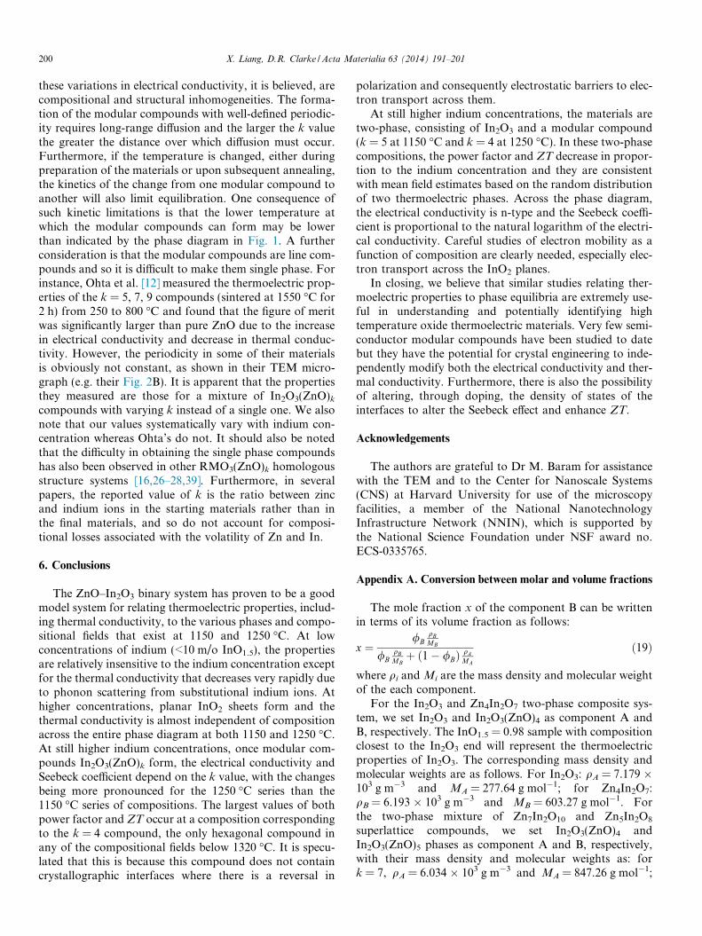
The relative insensitivity of the thermal conductivity toindium concentrations greater than �10 m/o InO1.5, meansthat the thermoelectric figure of merit ZT and the thermo-electric power factor S2r exhibit similar dependence onindium concentration. These trends are shown in Figs. 10and 11. The data indicate that the compounds k = 5 (at1150 �C) and k = 4 (at 1250 �C) have the largest values ofboth the thermoelectric power factor and ZT.
For compositions containing more indium than thesecompounds, the phase diagram, our XRD and our SEMand EDS analyses all indicate that the materials are two-phase. (There are also other two-phase regions consistingof mixtures of other modular compounds, albeit with anarrower range of composition, for instance between Zn7-
In2O10 and Zn5In2O8 compounds.) A striking feature ofthe data is that the power factor and figure of merit varyalmost linearly with concentration between the two phases,suggesting that the thermoelectric properties obey theequivalent of the Lever rule, with the value being aweighted average of the volume fractions of the two phases.It is therefore of interest to compare our data with themean field model presented by Bergman et al. [41,42] forthe thermoelectric properties of a composite consisting ofa randomly distributed mixture of two thermoelectricphases.
According to Bergman’s model, the thermoelectricpower factor of a random composite can be written interms of the volume fraction, /, and properties of thetwo phases, A and B, as:
ounds measured at 800 �C, together with values reported in the literature.
Seebeck coefficient (lV K�1)
Present work Literature
�241.2 �175 [44]�281.7 �24 [12]; �193 [44]; �60 [51]�360.5 �42 [12]; �198 [44]�360.9 �82 [12]; �207 [44]
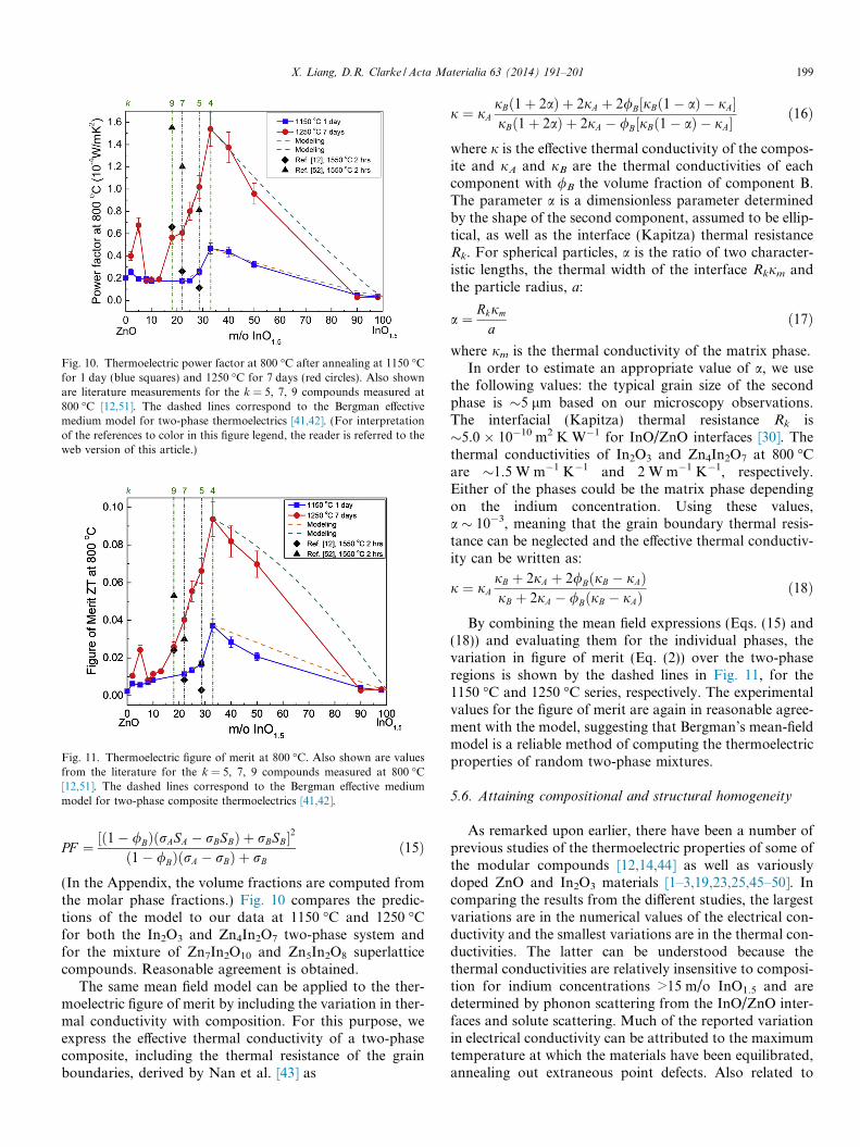
Fig. 10. Thermoelectric power factor at 800 �C after annealing at 1150 �Cfor 1 day (blue squares) and 1250 �C for 7 days (red circles). Also shownare literature measurements for the k = 5, 7, 9 compounds measured at800 �C [12,51]. The dashed lines correspond to the Bergman effectivemedium model for two-phase thermoelectrics [41,42]. (For interpretationof the references to color in this figure legend, the reader is referred to theweb version of this article.)
Fig. 11. Thermoelectric figure of merit at 800 �C. Also shown are valuesfrom the literature for the k = 5, 7, 9 compounds measured at 800 �C[12,51]. The dashed lines correspond to the Bergman effective mediummodel for two-phase composite thermoelectrics [41,42].
X. Liang, D.R. Clarke / Acta Materialia 63 (2014) 191–201 199
PF ¼ ½ð1� /BÞðrASA � rBSBÞ þ rBSB�2
ð1� /BÞðrA � rBÞ þ rBð15Þ
(In the Appendix, the volume fractions are computed fromthe molar phase fractions.) Fig. 10 compares the predic-tions of the model to our data at 1150 �C and 1250 �Cfor both the In2O3 and Zn4In2O7 two-phase system andfor the mixture of Zn7In2O10 and Zn5In2O8 superlatticecompounds. Reasonable agreement is obtained.
The same mean field model can be applied to the ther-moelectric figure of merit by including the variation in ther-mal conductivity with composition. For this purpose, weexpress the effective thermal conductivity of a two-phasecomposite, including the thermal resistance of the grainboundaries, derived by Nan et al. [43] as
j ¼ jAjBð1þ 2aÞ þ 2jA þ 2/B½jBð1� aÞ � jA�jBð1þ 2aÞ þ 2jA � /B½jBð1� aÞ � jA�
ð16Þ
where j is the effective thermal conductivity of the compos-ite and jA and jB are the thermal conductivities of eachcomponent with /B the volume fraction of component B.The parameter a is a dimensionless parameter determinedby the shape of the second component, assumed to be ellip-tical, as well as the interface (Kapitza) thermal resistanceRk. For spherical particles, a is the ratio of two character-istic lengths, the thermal width of the interface Rkjm andthe particle radius, a:
a ¼ Rkjm
að17Þ
where jm is the thermal conductivity of the matrix phase.In order to estimate an appropriate value of a, we use
the following values: the typical grain size of the secondphase is �5 lm based on our microscopy observations.The interfacial (Kapitza) thermal resistance Rk is�5.0 � 10�10 m2 K W�1 for InO/ZnO interfaces [30]. Thethermal conductivities of In2O3 and Zn4In2O7 at 800 �Care �1.5 W m�1 K�1 and 2 W m�1 K�1, respectively.Either of the phases could be the matrix phase dependingon the indium concentration. Using these values,a � 10�3, meaning that the grain boundary thermal resis-tance can be neglected and the effective thermal conductiv-ity can be written as:
j ¼ jAjB þ 2jA þ 2/BðjB � jAÞjB þ 2jA � /BðjB � jAÞ
ð18Þ
By combining the mean field expressions (Eqs. (15) and(18)) and evaluating them for the individual phases, thevariation in figure of merit (Eq. (2)) over the two-phaseregions is shown by the dashed lines in Fig. 11, for the1150 �C and 1250 �C series, respectively. The experimentalvalues for the figure of merit are again in reasonable agree-ment with the model, suggesting that Bergman’s mean-fieldmodel is a reliable method of computing the thermoelectricproperties of random two-phase mixtures.
5.6. Attaining compositional and structural homogeneity
As remarked upon earlier, there have been a number ofprevious studies of the thermoelectric properties of some ofthe modular compounds [12,14,44] as well as variouslydoped ZnO and In2O3 materials [1–3,19,23,25,45–50]. Incomparing the results from the different studies, the largestvariations are in the numerical values of the electrical con-ductivity and the smallest variations are in the thermal con-ductivities. The latter can be understood because thethermal conductivities are relatively insensitive to composi-tion for indium concentrations >15 m/o InO1.5 and aredetermined by phonon scattering from the InO/ZnO inter-faces and solute scattering. Much of the reported variationin electrical conductivity can be attributed to the maximumtemperature at which the materials have been equilibrated,annealing out extraneous point defects. Also related to
200 X. Liang, D.R. Clarke / Acta Materialia 63 (2014) 191–201
these variations in electrical conductivity, it is believed, arecompositional and structural inhomogeneities. The forma-tion of the modular compounds with well-defined periodic-ity requires long-range diffusion and the larger the k valuethe greater the distance over which diffusion must occur.Furthermore, if the temperature is changed, either duringpreparation of the materials or upon subsequent annealing,the kinetics of the change from one modular compound toanother will also limit equilibration. One consequence ofsuch kinetic limitations is that the lower temperature atwhich the modular compounds can form may be lowerthan indicated by the phase diagram in Fig. 1. A furtherconsideration is that the modular compounds are line com-pounds and so it is difficult to make them single phase. Forinstance, Ohta et al. [12] measured the thermoelectric prop-erties of the k = 5, 7, 9 compounds (sintered at 1550 �C for2 h) from 250 to 800 �C and found that the figure of meritwas significantly larger than pure ZnO due to the increasein electrical conductivity and decrease in thermal conduc-tivity. However, the periodicity in some of their materialsis obviously not constant, as shown in their TEM micro-graph (e.g. their Fig. 2B). It is apparent that the propertiesthey measured are those for a mixture of In2O3(ZnO)k
compounds with varying k instead of a single one. We alsonote that our values systematically vary with indium con-centration whereas Ohta’s do not. It should also be notedthat the difficulty in obtaining the single phase compoundshas also been observed in other RMO3(ZnO)k homologousstructure systems [16,26–28,39]. Furthermore, in severalpapers, the reported value of k is the ratio between zincand indium ions in the starting materials rather than inthe final materials, and so do not account for composi-tional losses associated with the volatility of Zn and In.
6. Conclusions
The ZnO–In2O3 binary system has proven to be a goodmodel system for relating thermoelectric properties, includ-ing thermal conductivity, to the various phases and compo-sitional fields that exist at 1150 and 1250 �C. At lowconcentrations of indium (<10 m/o InO1.5), the propertiesare relatively insensitive to the indium concentration exceptfor the thermal conductivity that decreases very rapidly dueto phonon scattering from substitutional indium ions. Athigher concentrations, planar InO2 sheets form and thethermal conductivity is almost independent of compositionacross the entire phase diagram at both 1150 and 1250 �C.At still higher indium concentrations, once modular com-pounds In2O3(ZnO)k form, the electrical conductivity andSeebeck coefficient depend on the k value, with the changesbeing more pronounced for the 1250 �C series than the1150 �C series of compositions. The largest values of bothpower factor and ZT occur at a composition correspondingto the k = 4 compound, the only hexagonal compound inany of the compositional fields below 1320 �C. It is specu-lated that this is because this compound does not containcrystallographic interfaces where there is a reversal in
polarization and consequently electrostatic barriers to elec-tron transport across them.
At still higher indium concentrations, the materials aretwo-phase, consisting of In2O3 and a modular compound(k = 5 at 1150 �C and k = 4 at 1250 �C). In these two-phasecompositions, the power factor and ZT decrease in propor-tion to the indium concentration and they are consistentwith mean field estimates based on the random distributionof two thermoelectric phases. Across the phase diagram,the electrical conductivity is n-type and the Seebeck coeffi-cient is proportional to the natural logarithm of the electri-cal conductivity. Careful studies of electron mobility as afunction of composition are clearly needed, especially elec-tron transport across the InO2 planes.
In closing, we believe that similar studies relating ther-moelectric properties to phase equilibria are extremely use-ful in understanding and potentially identifying hightemperature oxide thermoelectric materials. Very few semi-conductor modular compounds have been studied to datebut they have the potential for crystal engineering to inde-pendently modify both the electrical conductivity and ther-mal conductivity. Furthermore, there is also the possibilityof altering, through doping, the density of states of theinterfaces to alter the Seebeck effect and enhance ZT.
Acknowledgements
The authors are grateful to Dr M. Baram for assistancewith the TEM and to the Center for Nanoscale Systems(CNS) at Harvard University for use of the microscopyfacilities, a member of the National NanotechnologyInfrastructure Network (NNIN), which is supported bythe National Science Foundation under NSF award no.ECS-0335765.
Appendix A. Conversion between molar and volume fractions
The mole fraction x of the component B can be writtenin terms of its volume fraction as follows:
x ¼/B
qBMB
/BqBMBþ ð1� /BÞ qA
MA
ð19Þ
where qi and Mi are the mass density and molecular weightof the each component.
For the In2O3 and Zn4In2O7 two-phase composite sys-tem, we set In2O3 and In2O3(ZnO)4 as component A andB, respectively. The InO1.5 = 0.98 sample with compositionclosest to the In2O3 end will represent the thermoelectricproperties of In2O3. The corresponding mass density andmolecular weights are as follows. For In2O3: qA = 7.179 �103 g m�3 and MA = 277.64 g mol�1; for Zn4In2O7:qB = 6.193 � 103 g m�3 and MB = 603.27 g mol�1. Forthe two-phase mixture of Zn7In2O10 and Zn5In2O8
superlattice compounds, we set In2O3(ZnO)4 andIn2O3(ZnO)5 phases as component A and B, respectively,with their mass density and molecular weights as: fork = 7, qA = 6.034 � 103 g m�3 and MA = 847.26 g mol�1;
X. Liang, D.R. Clarke / Acta Materialia 63 (2014) 191–201 201
for k = 5, qB = 6.126 � 103 g m�3 and MB = 684.50 gmol�1. The mass densities of In2O3(ZnO)4, In2O3(ZnO)7
and In2O3(ZnO)5 were calculated based on the latticeparameter reported in the literature [16].
For the two-phase composite consisting of In2O3 andIn2O3(ZnO)4, the indium concentration can be furtherexpressed in terms of mole fraction of component B as,
½In� ¼ 2xþ 2ð1� xÞ4xþ 2xþ 2ð1� xÞ ð20Þ
Similarly for the two-phase mixture of In2O3(ZnO)7 andIn2O3(ZnO)5 superlattice compounds,
½In� ¼ 2xþ 2ð1� xÞ2xþ 2ð1� xÞ þ 5xþ 7ð1� xÞ ð21Þ
The above set of equations enables the two-phase com-posite thermoelectric power factor, which is originallyexpressed as a function of second-phase volume fraction,to be expressed and modeled as a function of indiumconcentration.
References
[1] Ohtaki M, Tsubota T, Eguchi K, Arai H. J Appl Phys 1996;79:1816.[2] Tsubota T, Ohtaki M, Eguchi K, Arai H. J Mater Chem 1997;7:85.[3] Cai KF, Muller E, Drasar C, Mrotzek A. Mater Sci Eng B – Solid
State Mater Adv Technol 2003;104:45.[4] Park K, Choi JW, Kim SJ, Kim GH, Cho YS. J Alloy Compd
2009;485:532.[5] White MA, Ochsenbein ST, Gamelin DR. Chem Mater 2008;20:7107.[6] Park K, Seong JK, Kim GH. J Alloy Compd 2009;473:423.[7] Colder H, Guilmeau E, Harnois C, Marinel S, Retoux R, Savary E. J
Eur Ceram Soc 2011;31:2957.[8] Park K, Ko KY. J Alloy Compd 2007;430:200.[9] Kishimoto K, Koyanagi T. J Appl Phys 2002;92:2544.
[10] Slack GA, Hussain MA. J Appl Phys 1991;70:2694.[11] Koumoto K, Terasaki I, Funahashi R. MRS Bull 2006;31:206.[12] Ohta H, Seo WS, Koumoto K. J Am Ceram Soc 1996;79:2193.[13] Masuda Y, Ohta M, Seo WS, Pitschke W, Koumoto K. J Solid State
Chem 2000;150:221.[14] Hirano S, Isobe S, Tani T, Kitamura N, Matsubara C, Koumoto K.
Jpn J Appl Phys Part 1 – Reg Pap Short Notes Rev Pap 2002;41:6430.[15] Hopper EM, Zhu QM, Song JH, Peng HW, Freeman AJ, Mason TO.
J Appl Phys 2011;109:6.[16] Moriga T, Edwards DD, Mason TO, Palmer GB, Poeppelmeier KR,
Schindler JL, et al. J Am Ceram Soc 1998;81:1310.[17] Veblen DR. Am Mineral 1991;76:801.[18] Snyder GJ, Toberer ES. Nat Mater 2008;7:105.
[19] Park K, Seong JK, Nahm S. J Alloy Compd 2008;455:331.[20] McCoy MA, Grimes RW, Lee WE. J Mater Res 1996;11:2009.[21] ICDD. PDF-4+ 2011 (Database). Newtown Square, PA, USA: Inter-
national Centre for Diffraction Data; 2011.[22] Barin I. Thermochemical data of pure substances. Weinheim: VCH;
1989.[23] Qu XR, Wang W, Lv SC, Jia DC. Solid State Commun 2011;151:332.[24] Bhosle V, Tiwari A, Narayan J. J Appl Phys 2006;100.[25] Yamaguchi H, Chonan Y, Oda M, Komiyama T, Aoyama T,
Sugiyama S. J Electron Mater 2011;40:723.[26] Nakamura M, Kimizuka N, Mohri T. J Solid State Chem
1991;93:298.[27] Nakamura M, Kimizuka N, Mohri T. J Solid State Chem 1990;86:16.[28] Kimizuka N, Isobe M, Nakamura M, Mohri T. J Solid State Chem
1993;103:394.[29] Uchida N, Bando Y, Nakamura M, Kimizuka N. J Electron Microsc
1994;43:146.[30] Liang X, Baram M, Clarke DR. Appl Phys Lett 2013.[31] Tritt TM. In: Clarke DR, Fratzl P, editors. Annual review of
materials research, vol. 41; 2011. p. 433.[32] Callaway J, von Baeyer HC. Phys Rev 1960;120:1149.[33] Clarke DR. Surf Coat Technol 2003;163–164:67.[34] Roufosse MC, Klemens PG. J Geophys Res 1974;79:703.[35] Cahill DG, Pohl RO. Annu Rev Phys Chem 1988;39:93.[36] McCoy MA, Grimes RW, Lee WE. Philos Mag A – Phys Condens
Matter Struct Def Mech Prop 1997;76:1187.[37] Harvey SP, Poeppelmeier KR, Mason TO. J Am Ceram Soc
2008;91:3683.[38] Hopper EM, Zhu QM, Song JH, Peng HW, Freeman AJ, Mason TO.
J Appl Phys 2011;109.[39] Kimizuka N, Isobe M, Nakamura M. J Solid State Chem
1995;116:170.[40] Nakamura M, Kimizuka N, Mohri T, Isobe M. J Solid State Chem
1993;105:535.[41] Bergman DJ, Fel LG. J Appl Phys 1999;85:8205.[42] Bergman DJ, Levy O. J Appl Phys 1991;70:6821.[43] Nan CW, Birringer R, Clarke DR, Gleiter H. J Appl Phys
1997;81:6692.[44] Kaga H, Asahi R, Tani T. Jpn J Appl Phys Part 1 – Reg Pap Short
Notes Rev Pap 2004;43:3540.[45] Ohtaki M, Ogura D, Eguchi K, Arai H. J Mater Chem 1994;4:653.[46] Berardan D, Guilmeau E, Maignan A, Raveau B. Solid State
Commun 2008;146:97.[47] Liu Y, Lin Y-H, Lan J, Xu W, Zhang B-P, Nan C-W, et al. J Am
Ceram Soc 2010;93:2938.[48] Cheng B, Fang H, Lan JL, Liu Y, Lin YH, Nan CW. J Am Ceram
Soc 2011;94:2279.[49] Liu Y, Lin YH, Lan JL, Zhang BP, Xu W, Nan CW, et al. J Electron
Mater 2011;40:1083.[50] Park K, Seong JK, Kwon Y, Nahm S, Cho WS. Mater Res Bull
2008;43:54.[51] Kazeoka M, Hiramatsu H, Seo WS, Koumoto K. J Mater Res
1998;13:523.