Embed Size (px)
Citation preview
FN9111Rev.7.00
Jul 7, 2017
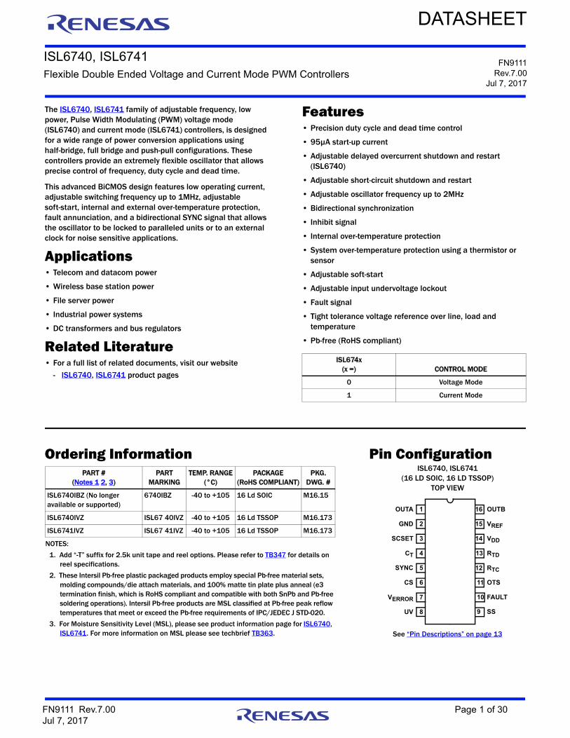
ISL6740, ISL6741Flexible Double Ended Voltage and Current Mode PWM Controllers
DATASHEET
The ISL6740, ISL6741 family of adjustable frequency, low power, Pulse Width Modulating (PWM) voltage mode (ISL6740) and current mode (ISL6741) controllers, is designed for a wide range of power conversion applications using half-bridge, full bridge and push-pull configurations. These controllers provide an extremely flexible oscillator that allows precise control of frequency, duty cycle and dead time.
This advanced BiCMOS design features low operating current, adjustable switching frequency up to 1MHz, adjustable soft-start, internal and external over-temperature protection, fault annunciation, and a bidirectional SYNC signal that allows the oscillator to be locked to paralleled units or to an external clock for noise sensitive applications.
Applications• Telecom and datacom power
• Wireless base station power
• File server power
• Industrial power systems
• DC transformers and bus regulators
Related Literature• For a full list of related documents, visit our website
- ISL6740, ISL6741 product pages
Features• Precision duty cycle and dead time control
• 95µA start-up current
• Adjustable delayed overcurrent shutdown and restart (ISL6740)
• Adjustable short-circuit shutdown and restart
• Adjustable oscillator frequency up to 2MHz
• Bidirectional synchronization
• Inhibit signal
• Internal over-temperature protection
• System over-temperature protection using a thermistor or sensor
• Adjustable soft-start
• Adjustable input undervoltage lockout
• Fault signal
• Tight tolerance voltage reference over line, load and temperature
• Pb-free (RoHS compliant)
ISL674x(x =) CONTROL MODE
0 Voltage Mode
1 Current Mode
Ordering Information Pin ConfigurationISL6740, ISL6741
(16 LD SOIC, 16 LD TSSOP)TOP VIEW
See “Pin Descriptions” on page 13
PART #(Notes 1 2, 3)
PARTMARKING
TEMP. RANGE(°C)
PACKAGE(RoHS COMPLIANT)
PKG.DWG. #
ISL6740IBZ (No longer available or supported)
6740IBZ -40 to +105 16 Ld SOIC M16.15
ISL6740IVZ ISL67 40IVZ -40 to +105 16 Ld TSSOP M16.173
ISL6741IVZ ISL67 41IVZ -40 to +105 16 Ld TSSOP M16.173
NOTES:
1. Add “-T” suffix for 2.5k unit tape and reel options. Please refer to TB347 for details on reel specifications.
2. These Intersil Pb-free plastic packaged products employ special Pb-free material sets, molding compounds/die attach materials, and 100% matte tin plate plus anneal (e3 termination finish, which is RoHS compliant and compatible with both SnPb and Pb-free soldering operations). Intersil Pb-free products are MSL classified at Pb-free peak reflow temperatures that meet or exceed the Pb-free requirements of IPC/JEDEC J STD-020.
3. For Moisture Sensitivity Level (MSL), please see product information page for ISL6740, ISL6741. For more information on MSL please see techbrief TB363.
OUTA
GND
SCSET
CT
SYNC
CS
VERROR
OUTB
VREF
VDD
RTD
RTC
OTS
FAULT
1
2
3
4
5
6
7
16
15
14
13
12
11
10
8 9UV SS
FN9111 Rev.7.00 Page 1 of 30Jul 7, 2017
ISL6740, ISL6741
Table of ContentsFunctional Block Diagrams . . . . . . . . . . . . . . . . . . . . . . . . . . . . . . . . . . . . . . . . . . . . . . . . . . . . . . . . . . . . . . . . . . . . . . . . . . . . . . . . . . . 3
Typical Application (ISL6740EVAL1) - 48V Input DC Transformer, 12V at 8A Output. . . . . . . . . . . . . . . . . . . . . . . . . . . . . . . . . . . . 5ISL6740EVAL1 Component List. . . . . . . . . . . . . . . . . . . . . . . . . . . . . . . . . . . . . . . . . . . . . . . . . . . . . . . . . . . . . . . . . . . . . . . . . . . . . . . . . . . . . .6
Typical Application (ISL6740EVAL2Z) - 36V to 75V Input, Regulated 12V at 8A Output . . . . . . . . . . . . . . . . . . . . . . . . . . . . . . . . . 7ISL6740EVAL2Z Component List . . . . . . . . . . . . . . . . . . . . . . . . . . . . . . . . . . . . . . . . . . . . . . . . . . . . . . . . . . . . . . . . . . . . . . . . . . . . . . . . . . . .8
Typical Application (ISL6741) - 48V to 5V Push-Pull DC/DC Converter . . . . . . . . . . . . . . . . . . . . . . . . . . . . . . . . . . . . . . . . . . . . . . . 9
Absolute Maximum Ratings . . . . . . . . . . . . . . . . . . . . . . . . . . . . . . . . . . . . . . . . . . . . . . . . . . . . . . . . . . . . . . . . . . . . . . . . . . . . . . . . . . 10
Thermal Information . . . . . . . . . . . . . . . . . . . . . . . . . . . . . . . . . . . . . . . . . . . . . . . . . . . . . . . . . . . . . . . . . . . . . . . . . . . . . . . . . . . . . . . . 10
Operating Conditions . . . . . . . . . . . . . . . . . . . . . . . . . . . . . . . . . . . . . . . . . . . . . . . . . . . . . . . . . . . . . . . . . . . . . . . . . . . . . . . . . . . . . . . 10
Electrical Specifications . . . . . . . . . . . . . . . . . . . . . . . . . . . . . . . . . . . . . . . . . . . . . . . . . . . . . . . . . . . . . . . . . . . . . . . . . . . . . . . . . . . . 10
Typical Performance Curves . . . . . . . . . . . . . . . . . . . . . . . . . . . . . . . . . . . . . . . . . . . . . . . . . . . . . . . . . . . . . . . . . . . . . . . . . . . . . . . . . 13
Pin Descriptions. . . . . . . . . . . . . . . . . . . . . . . . . . . . . . . . . . . . . . . . . . . . . . . . . . . . . . . . . . . . . . . . . . . . . . . . . . . . . . . . . . . . . . . . . . . . 13
Functional Description . . . . . . . . . . . . . . . . . . . . . . . . . . . . . . . . . . . . . . . . . . . . . . . . . . . . . . . . . . . . . . . . . . . . . . . . . . . . . . . . . . . . . . 14Features . . . . . . . . . . . . . . . . . . . . . . . . . . . . . . . . . . . . . . . . . . . . . . . . . . . . . . . . . . . . . . . . . . . . . . . . . . . . . . . . . . . . . . . . . . . . . . . . . . . . . . . 14Oscillator . . . . . . . . . . . . . . . . . . . . . . . . . . . . . . . . . . . . . . . . . . . . . . . . . . . . . . . . . . . . . . . . . . . . . . . . . . . . . . . . . . . . . . . . . . . . . . . . . . . . . . . 14Implementing Synchronization . . . . . . . . . . . . . . . . . . . . . . . . . . . . . . . . . . . . . . . . . . . . . . . . . . . . . . . . . . . . . . . . . . . . . . . . . . . . . . . . . . . . 15Soft-Start Operation. . . . . . . . . . . . . . . . . . . . . . . . . . . . . . . . . . . . . . . . . . . . . . . . . . . . . . . . . . . . . . . . . . . . . . . . . . . . . . . . . . . . . . . . . . . . . . 15Gate Drive . . . . . . . . . . . . . . . . . . . . . . . . . . . . . . . . . . . . . . . . . . . . . . . . . . . . . . . . . . . . . . . . . . . . . . . . . . . . . . . . . . . . . . . . . . . . . . . . . . . . . . 15Undervoltage Monitor and Inhibit . . . . . . . . . . . . . . . . . . . . . . . . . . . . . . . . . . . . . . . . . . . . . . . . . . . . . . . . . . . . . . . . . . . . . . . . . . . . . . . . . . 15Overcurrent Operation. . . . . . . . . . . . . . . . . . . . . . . . . . . . . . . . . . . . . . . . . . . . . . . . . . . . . . . . . . . . . . . . . . . . . . . . . . . . . . . . . . . . . . . . . . . . 16Short Circuit Operation . . . . . . . . . . . . . . . . . . . . . . . . . . . . . . . . . . . . . . . . . . . . . . . . . . . . . . . . . . . . . . . . . . . . . . . . . . . . . . . . . . . . . . . . . . . 16Fault Conditions . . . . . . . . . . . . . . . . . . . . . . . . . . . . . . . . . . . . . . . . . . . . . . . . . . . . . . . . . . . . . . . . . . . . . . . . . . . . . . . . . . . . . . . . . . . . . . . . . 16Thermal Protection . . . . . . . . . . . . . . . . . . . . . . . . . . . . . . . . . . . . . . . . . . . . . . . . . . . . . . . . . . . . . . . . . . . . . . . . . . . . . . . . . . . . . . . . . . . . . . 16Ground Plane Requirements . . . . . . . . . . . . . . . . . . . . . . . . . . . . . . . . . . . . . . . . . . . . . . . . . . . . . . . . . . . . . . . . . . . . . . . . . . . . . . . . . . . . . . 17Typical Application . . . . . . . . . . . . . . . . . . . . . . . . . . . . . . . . . . . . . . . . . . . . . . . . . . . . . . . . . . . . . . . . . . . . . . . . . . . . . . . . . . . . . . . . . . . . . . . 17Circuit Element Descriptions . . . . . . . . . . . . . . . . . . . . . . . . . . . . . . . . . . . . . . . . . . . . . . . . . . . . . . . . . . . . . . . . . . . . . . . . . . . . . . . . . . . . . . 17Design Criteria . . . . . . . . . . . . . . . . . . . . . . . . . . . . . . . . . . . . . . . . . . . . . . . . . . . . . . . . . . . . . . . . . . . . . . . . . . . . . . . . . . . . . . . . . . . . . . . . . . 17Transformer Design. . . . . . . . . . . . . . . . . . . . . . . . . . . . . . . . . . . . . . . . . . . . . . . . . . . . . . . . . . . . . . . . . . . . . . . . . . . . . . . . . . . . . . . . . . . . . . 17MOSFET Selection . . . . . . . . . . . . . . . . . . . . . . . . . . . . . . . . . . . . . . . . . . . . . . . . . . . . . . . . . . . . . . . . . . . . . . . . . . . . . . . . . . . . . . . . . . . . . . . 20Oscillator Component Selection . . . . . . . . . . . . . . . . . . . . . . . . . . . . . . . . . . . . . . . . . . . . . . . . . . . . . . . . . . . . . . . . . . . . . . . . . . . . . . . . . . . 20Output Filter Design. . . . . . . . . . . . . . . . . . . . . . . . . . . . . . . . . . . . . . . . . . . . . . . . . . . . . . . . . . . . . . . . . . . . . . . . . . . . . . . . . . . . . . . . . . . . . . 21Overcurrent Component Selection . . . . . . . . . . . . . . . . . . . . . . . . . . . . . . . . . . . . . . . . . . . . . . . . . . . . . . . . . . . . . . . . . . . . . . . . . . . . . . . . . 21Performance. . . . . . . . . . . . . . . . . . . . . . . . . . . . . . . . . . . . . . . . . . . . . . . . . . . . . . . . . . . . . . . . . . . . . . . . . . . . . . . . . . . . . . . . . . . . . . . . . . . . 22Waveforms . . . . . . . . . . . . . . . . . . . . . . . . . . . . . . . . . . . . . . . . . . . . . . . . . . . . . . . . . . . . . . . . . . . . . . . . . . . . . . . . . . . . . . . . . . . . . . . . . . . . . 22
Adding Line Only Regulation - Feed Forward. . . . . . . . . . . . . . . . . . . . . . . . . . . . . . . . . . . . . . . . . . . . . . . . . . . . . . . . . . . . . . . . . . . . 23
Adding Regulation - Closed Loop Feedback . . . . . . . . . . . . . . . . . . . . . . . . . . . . . . . . . . . . . . . . . . . . . . . . . . . . . . . . . . . . . . . . . . . . 24Performance. . . . . . . . . . . . . . . . . . . . . . . . . . . . . . . . . . . . . . . . . . . . . . . . . . . . . . . . . . . . . . . . . . . . . . . . . . . . . . . . . . . . . . . . . . . . . . . . . . . . 27References . . . . . . . . . . . . . . . . . . . . . . . . . . . . . . . . . . . . . . . . . . . . . . . . . . . . . . . . . . . . . . . . . . . . . . . . . . . . . . . . . . . . . . . . . . . . . . . . . . . . . 27
Revision History. . . . . . . . . . . . . . . . . . . . . . . . . . . . . . . . . . . . . . . . . . . . . . . . . . . . . . . . . . . . . . . . . . . . . . . . . . . . . . . . . . . . . . . . . . . . 28
About Intersil . . . . . . . . . . . . . . . . . . . . . . . . . . . . . . . . . . . . . . . . . . . . . . . . . . . . . . . . . . . . . . . . . . . . . . . . . . . . . . . . . . . . . . . . . . . . . . 28
Package Outline Drawing . . . . . . . . . . . . . . . . . . . . . . . . . . . . . . . . . . . . . . . . . . . . . . . . . . . . . . . . . . . . . . . . . . . . . . . . . . . . . . . . . . . . 29
Small Outline Plastic Packages (SOIC). . . . . . . . . . . . . . . . . . . . . . . . . . . . . . . . . . . . . . . . . . . . . . . . . . . . . . . . . . . . . . . . . . . . . . . . . 30
FN9111 Rev.7.00 Page 2 of 30Jul 7, 2017
FN
9111
Re
v.7.0
0P
age 3 of 3
0Jul 7, 2017
ISL6
740
, ISL6
741
OUTA
OUTB
VREF
SS
ON
ATCH
4.25V
0.27VSS LOW
FAULT LATCHSET DOMINANT
FL
VREFVREF UV 4.65V
FAULT
OC S/D
OC S/D
SC S/D
SS HI +-
+-
+-
Q
Q
S
R
Q
Q
70µA
15µA
+-BG
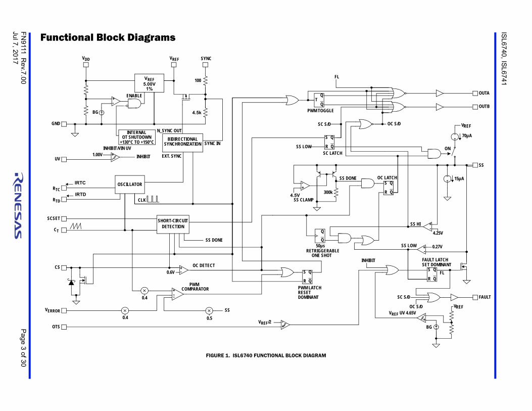
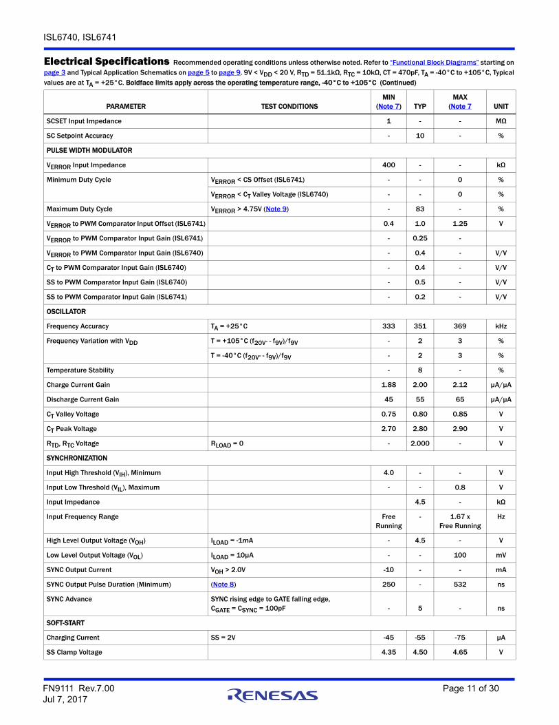
Functional Block Diagrams
FIGURE 1. ISL6740 FUNCTIONAL BLOCK DIAGRAM
VREF5.00V
1%
GND
VDD VREF SYNC
ENABLE
UV
SCSET
RTD
1.00V
CT
IRTD
EXT. SYNC
CLK
INHIBIT/VIN UV
INHIBIT
FL
0.4
CS
VERROR0.5
SS
PWMCOMPARATOR
N_SYNC OUT
0.6V
0.4
OC DETECT
PWM LATCHRESETDOMINANT
OC L
4.5VSS CLAMP
OTS
PWM TOGGLE
VREF/2
INHIBIT
SS DONE
SS LOWSC LATCH
SC S/D
300k
100
4.5k
BIDIRECTIONALSYNCHRONIZATION SYNC IN
OSCILLATOR
SHORT-CIRCUITDETECTION
+-
+-
RTCIRTC
+--
S
R
S
R
Q
Q
S
R
Q
Q
SS DONE
+-
+-
+-BG
TQ
Q
Q
Q50µs
RETRIGGERABLEONE SHOT
+-
INTERNALOT SHUTDOWN
+130°C TO +150°C
FN
9111
Re
v.7.0
0P
age 4 of 3
0Jul 7, 2017
ISL6
740
, ISL6
741
OUTA
OUTB
VREF
SS
ON
0.27VSS LOW
FAULT LATCHSET DOMINANT
FL
VREFF UV 4.65V
FAULTSC S/D
+-
+-
S
R
Q
Q
70µA
15µA
+-BG
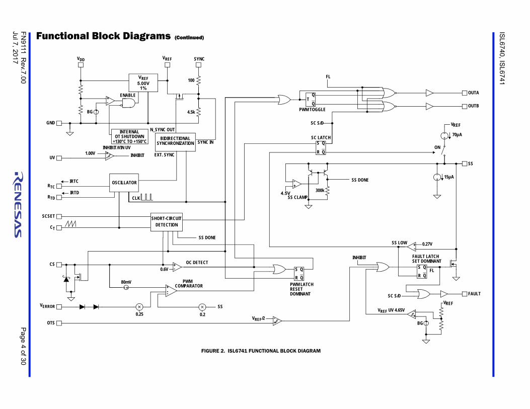
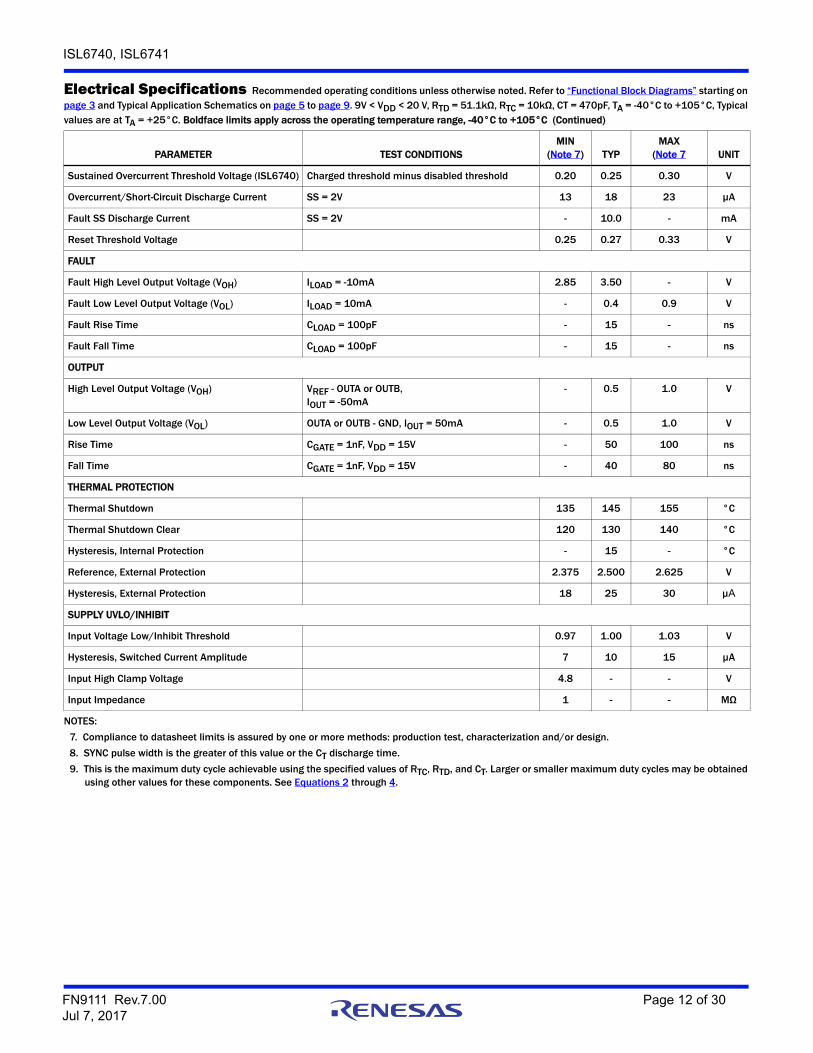
FIGURE 2. ISL6741 FUNCTIONAL BLOCK DIAGRAM
Functional Block Diagrams (Continued)
GND
VDD VREF SYNC
ENABLE
UV
SCSET
RTD
1.00V
CT
IRTD
EXT. SYNC
CLK
INHIBIT/VIN UVINHIBIT
FL
80mV
0.25
CS
VERROR
0.2SS
PWMCOMPARATOR
N_SYNC OUT
0.6VOC DETECT
PWM LATCHRESETDOMINANT
4.5V
VRE
SS CLAMP
OTS
PWM TOGGLE
VREF/2
INHIBIT
SS DONE
SC LATCH
SC S/D
300k
100
4.5k
SYNC IN
OSCILLATOR
SHORT-CIRCUITDETECTION
+-
+-
RTCIRTC
+- +--
S
R
Q
Q
S
R
Q
Q
SS DONE
+-
+-
+-BG
TQ
Q
+-
BIDIRECTIONALSYNCHRONIZATION
INTERNALOT SHUTDOWN
+130°C TO +150°C
VREF5.00V
1%
FN
9111
Re
v.7.0
0P
age 5 of 3
0Jul 7, 2017
ISL6
740
, ISL6
741
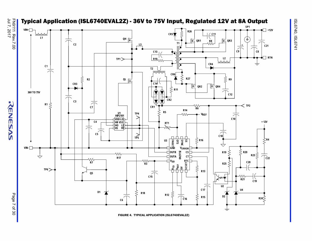
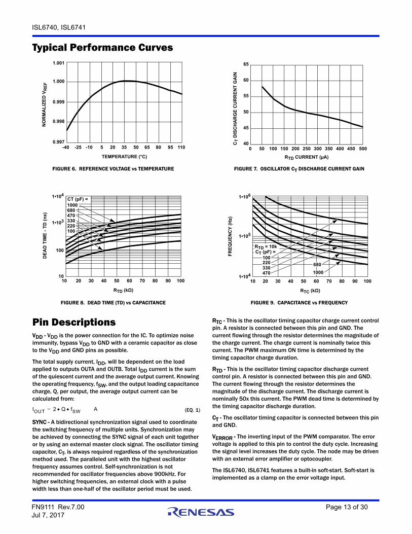
8A Output
+12V
RTN
C10
C18
C8
L2
C9
QR4
QR3
R9
C12
TP2
SP1
Typical Application (ISL6740EVAL1) - 48V Input DC Transformer, 12V atVIN+
VIN-
HIP2101VDDHBHOHS
LO
LIHI
VSS
VREF
CR2R6
R14
RT1
R19
R13
R15C16
C17R18
C6
R17
R2
R7
Q5
C4
C5
QL
QHC2
C3
C1
R1
R5
L1
U1
U3
CR1
T1
T2
R12D1
QR1
QR2
L3
C13
R10
C14 R11
R3
C15
R8
C11
CR3
TP6
TP4
TP5
TP1
C7
ISL6740
GND
RTD
VDD
VREF
SYNC
UV SCSE
T
RTCCTCS
VERROR
FAULTOTS SS
OUTBOUTA
U1
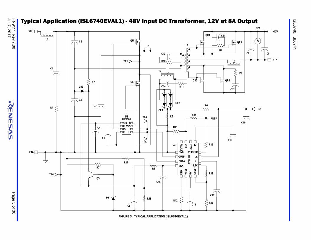
FIGURE 3. TYPICAL APPLICATION (ISL6740EVAL1)
ISL6740, ISL6741
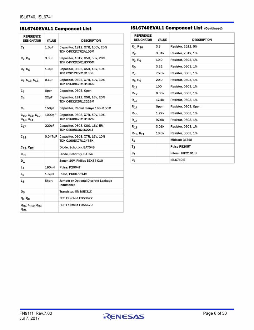
ISL6740EVAL1 Component List REFERENCEDESIGNATOR VALUE DESCRIPTION
C1 1.0µF Capacitor, 1812, X7R, 100V, 20%TDK C4532X7R2A105M
C2, C3 3.3µF Capacitor, 1812, X5R, 50V, 20%TDK C4532X5R1H335M
C4, C6 1.0µF Capacitor, 0805, X5R, 16V, 10%TDK C2012X5R1C105K
C5, C15, C16 0.1µF Capacitor, 0603, X7R, 50V, 10%TDK C1608X7R1H104K
C7 Open Capacitor, 0603, Open
C8 22µF Capacitor, 1812, X5R, 16V, 20%TDK C4532X5R1C226M
C9 150µF Capacitor, Radial, Sanyo 16SH150M
C10, C11, C12, C13, C14
1000pF Capacitor, 0603, X7R, 50V, 10%TDK C1608X7R1H102K
C17 220pF Capacitor, 0603, COG, 16V, 5%TDK C1608COG1C221J
C18 0.047µF Capacitor, 0603, X7R, 16V, 10%TDK C1608X7R1C473K
CR1, CR2 Diode, Schottky, BAT54S
CR3 Diode, Schottky, BAT54
D1 Zener, 10V, Philips BZX84-C10
L1 190nH Pulse, P2004T
L2 1.5µH Pulse, PG0077.142
L3 Short Jumper or Optional Discrete Leakage Inductance
Q5 Transistor, ON MJD31C
QL, QH FET, Fairchild FDS3672
QR1, QR2, QR3, QR4
FET, Fairchild FDS5670
R1, R10 3.3 Resistor, 2512, 5%
R2 3.01k Resistor, 2512, 1%
R3, R6 10.0 Resistor, 0603, 1%
R5 3.32 Resistor, 0603, 1%
R7 75.0k Resistor, 0805, 1%
R8, R9 20.0 Resistor, 0805, 1%
R11 100 Resistor, 0603, 1%
R12 8.06k Resistor, 0603, 1%
R13 17.4k Resistor, 0603, 1%
R14 Open Resistor, 0603, Open
R15 1.27k Resistor, 0603, 1%
R17 97.6k Resistor, 0603, 1%
R18 3.01k Resistor, 0603, 1%
R19, RT1 10.0k Resistor, 0603, 1%
T1 Midcom 31718
T2 Pulse P8205T
U1 Intersil HIP2101IB
U3 ISL6740IB
ISL6740EVAL1 Component List (Continued)
REFERENCEDESIGNATOR VALUE DESCRIPTION
FN9111 Rev.7.00 Page 6 of 30Jul 7, 2017
FN
9111
Re
v.7.0
0P
age 7 of 3
0Jul 7, 2017
ISL6
740
, ISL6
741
at 8A Output+12V
RTN
C10
C8C9
QR3
R9
C12
TP2
SP1
R23
R24
R21
C20
C19
U4
+ 12V
R20
R4
C22
C21+
Typical Application (ISL6740EVAL2Z) - 36V to 75V Input, Regulated 12VVIN+
VIN-
HIP2101VDDHBHOHS
LO
LIHI
VSS
VREF
CR2
R6R14
RT1
R16
R13
R15C16
C17
C18
R18
C6
R17
R2
R7
Q5
C4
C5
QL
QH
C2
C3
C1
R1
R5
L1
36V TO 75V
U1
U3
CR1
L2
T1
T2
R12D1
QR1
QR2
L3
C13
R10
C14
R11
R3
C15
QR4
R8
C11
CR3
TP6
TP4
TP5
TP1
C7
U2
R19
ISL6740
GND
R TD
VDD
V REF
SYNC
UV SCSE
TRTCCTCS
VERROR
FAULTOTS SS
OUTBOUTA
CR5R26
D2
R25
CR6R27
CR4
FIGURE 4. TYPICAL APPLICATION (ISL6740EVAL2Z)
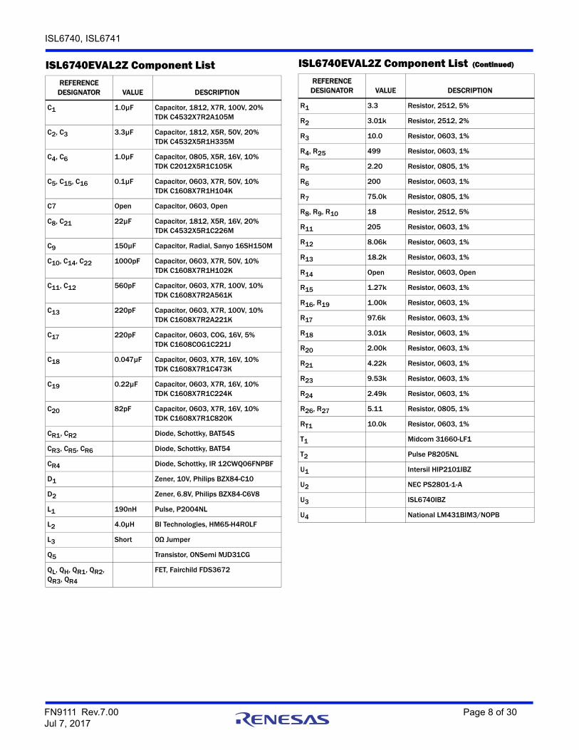
ISL6740, ISL6741
ISL6740EVAL2Z Component List REFERENCE DESIGNATOR VALUE DESCRIPTION
C1 1.0µF Capacitor, 1812, X7R, 100V, 20%TDK C4532X7R2A105M
C2, C3 3.3µF Capacitor, 1812, X5R, 50V, 20%TDK C4532X5R1H335M
C4, C6 1.0µF Capacitor, 0805, X5R, 16V, 10%TDK C2012X5R1C105K
C5, C15, C16 0.1µF Capacitor, 0603, X7R, 50V, 10%TDK C1608X7R1H104K
C7 Open Capacitor, 0603, Open
C8, C21 22µF Capacitor, 1812, X5R, 16V, 20%TDK C4532X5R1C226M
C9 150µF Capacitor, Radial, Sanyo 16SH150M
C10, C14, C22 1000pF Capacitor, 0603, X7R, 50V, 10%TDK C1608X7R1H102K
C11, C12 560pF Capacitor, 0603, X7R, 100V, 10%TDK C1608X7R2A561K
C13 220pF Capacitor, 0603, X7R, 100V, 10%TDK C1608X7R2A221K
C17 220pF Capacitor, 0603, COG, 16V, 5%TDK C1608COG1C221J
C18 0.047µF Capacitor, 0603, X7R, 16V, 10%TDK C1608X7R1C473K
C19 0.22µF Capacitor, 0603, X7R, 16V, 10%TDK C1608X7R1C224K
C20 82pF Capacitor, 0603, X7R, 16V, 10%TDK C1608X7R1C820K
CR1, CR2 Diode, Schottky, BAT54S
CR3, CR5, CR6 Diode, Schottky, BAT54
CR4 Diode, Schottky, IR 12CWQ06FNPBF
D1 Zener, 10V, Philips BZX84-C10
D2 Zener, 6.8V, Philips BZX84-C6V8
L1 190nH Pulse, P2004NL
L2 4.0µH BI Technologies, HM65-H4R0LF
L3 Short 0Ω Jumper
Q5 Transistor, ONSemi MJD31CG
QL, QH, QR1, QR2, QR3, QR4
FET, Fairchild FDS3672
R1 3.3 Resistor, 2512, 5%
R2 3.01k Resistor, 2512, 2%
R3 10.0 Resistor, 0603, 1%
R4, R25 499 Resistor, 0603, 1%
R5 2.20 Resistor, 0805, 1%
R6 200 Resistor, 0603, 1%
R7 75.0k Resistor, 0805, 1%
R8, R9, R10 18 Resistor, 2512, 5%
R11 205 Resistor, 0603, 1%
R12 8.06k Resistor, 0603, 1%
R13 18.2k Resistor, 0603, 1%
R14 Open Resistor, 0603, Open
R15 1.27k Resistor, 0603, 1%
R16, R19 1.00k Resistor, 0603, 1%
R17 97.6k Resistor, 0603, 1%
R18 3.01k Resistor, 0603, 1%
R20 2.00k Resistor, 0603, 1%
R21 4.22k Resistor, 0603, 1%
R23 9.53k Resistor, 0603, 1%
R24 2.49k Resistor, 0603, 1%
R26, R27 5.11 Resistor, 0805, 1%
RT1 10.0k Resistor, 0603, 1%
T1 Midcom 31660-LF1
T2 Pulse P8205NL
U1 Intersil HIP2101IBZ
U2 NEC PS2801-1-A
U3 ISL6740IBZ
U4 National LM431BIM3/NOPB
ISL6740EVAL2Z Component List (Continued)
REFERENCE DESIGNATOR VALUE DESCRIPTION
FN9111 Rev.7.00 Page 8 of 30Jul 7, 2017
FN
9111
Re
v.7.0
0P
age 9 of 3
0Jul 7, 2017
ISL6
740
, ISL6
741
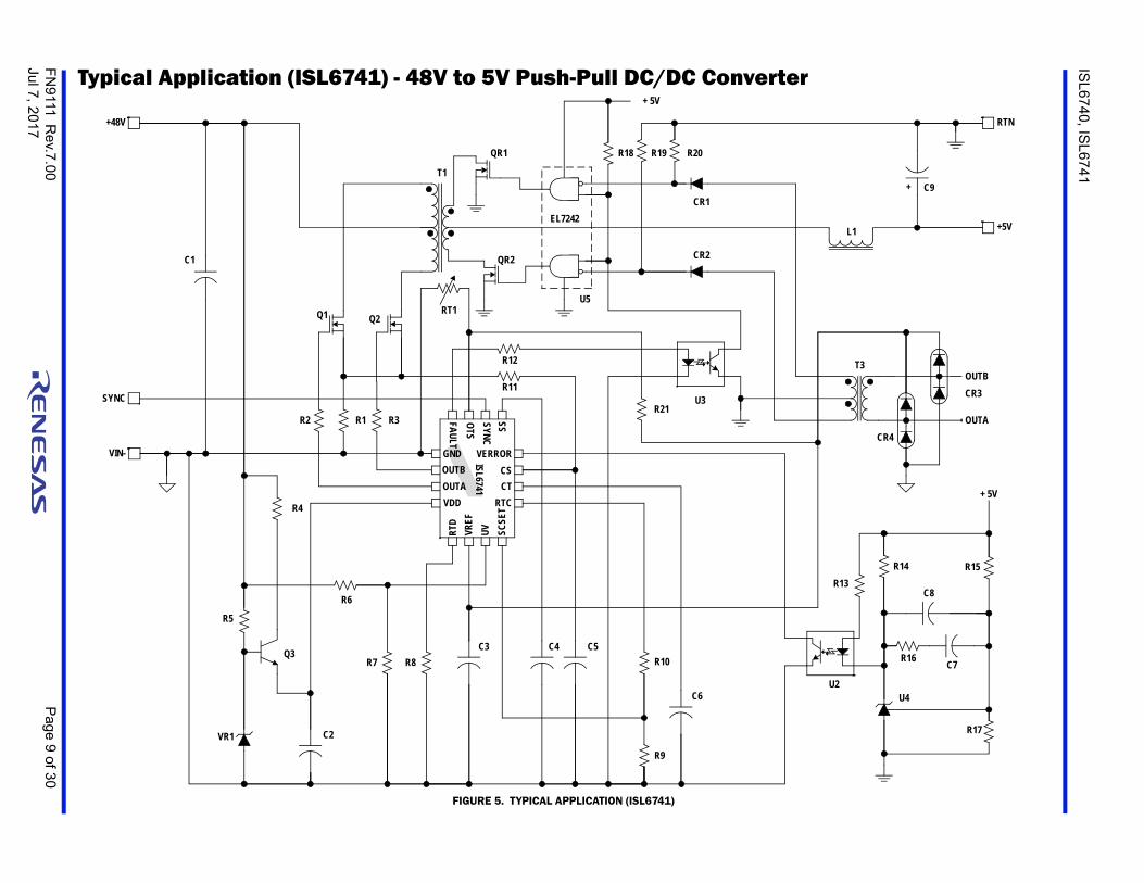
+5V
RTN
C9
L1
R15
R17
R16
C8
C7
U2U4
+ 5V
R13R14
T3
OUTA
OUTB
CR4
CR3
+
Typical Application (ISL6741) - 48V to 5V Push-Pull DC/DC Converter
+48V
VIN-
R10
R9
C5
C6
R7
C2
R6
R4
R5
Q3
Q1 Q2
C1
T1
VR1
QR1
QR2
C3
ISL6741
GNDRT
D
VDD
VREF
SYNC
UV SCSE
TRTCCTCS
VERROR
FAULTOTS SS
OUTBOUTA
U5
R19 R20
+ 5V
R18
U3
CR1
CR2
EL7242
SYNC
R2 R3R1
R8C4
R11
R12
RT1
R21
FIGURE 5. TYPICAL APPLICATION (ISL6741)
ISL6740, ISL6741
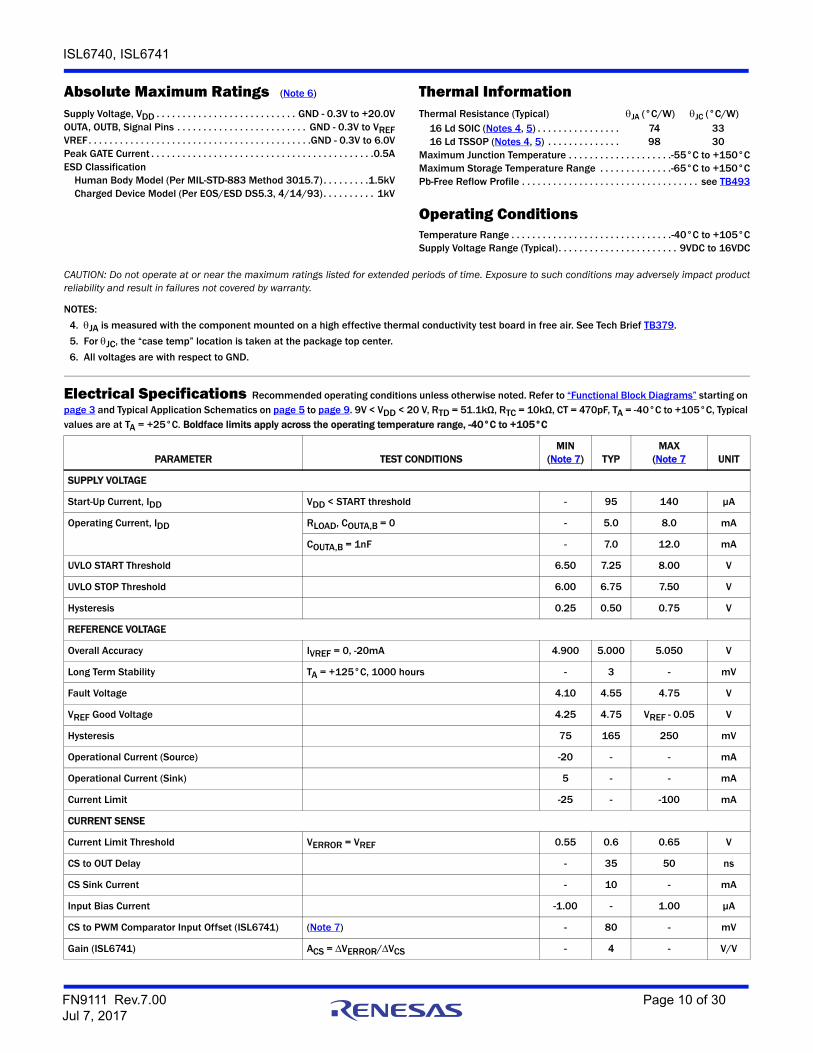
Absolute Maximum Ratings (Note 6) Thermal InformationSupply Voltage, VDD . . . . . . . . . . . . . . . . . . . . . . . . . . . GND - 0.3V to +20.0VOUTA, OUTB, Signal Pins . . . . . . . . . . . . . . . . . . . . . . . . . GND - 0.3V to VREFVREF . . . . . . . . . . . . . . . . . . . . . . . . . . . . . . . . . . . . . . . . . . .GND - 0.3V to 6.0VPeak GATE Current . . . . . . . . . . . . . . . . . . . . . . . . . . . . . . . . . . . . . . . . . . .0.5AESD Classification
Human Body Model (Per MIL-STD-883 Method 3015.7) . . . . . . . . .1.5kVCharged Device Model (Per EOS/ESD DS5.3, 4/14/93). . . . . . . . . . 1kV
Thermal Resistance (Typical) JA (°C/W) JC (°C/W)16 Ld SOIC (Notes 4, 5) . . . . . . . . . . . . . . . . 74 3316 Ld TSSOP (Notes 4, 5) . . . . . . . . . . . . . . 98 30
Maximum Junction Temperature . . . . . . . . . . . . . . . . . . . .-55°C to +150°CMaximum Storage Temperature Range . . . . . . . . . . . . . .-65°C to +150°CPb-Free Reflow Profile . . . . . . . . . . . . . . . . . . . . . . . . . . . . . . . . . . see TB493
Operating ConditionsTemperature Range . . . . . . . . . . . . . . . . . . . . . . . . . . . . . . .-40°C to +105°CSupply Voltage Range (Typical). . . . . . . . . . . . . . . . . . . . . . . 9VDC to 16VDC
CAUTION: Do not operate at or near the maximum ratings listed for extended periods of time. Exposure to such conditions may adversely impact productreliability and result in failures not covered by warranty.
NOTES:
4. JA is measured with the component mounted on a high effective thermal conductivity test board in free air. See Tech Brief TB379.
5. For JC, the “case temp” location is taken at the package top center.
6. All voltages are with respect to GND.
Electrical Specifications Recommended operating conditions unless otherwise noted. Refer to “Functional Block Diagrams” starting on page 3 and Typical Application Schematics on page 5 to page 9. 9V < VDD < 20 V, RTD = 51.1kΩ, RTC = 10kΩ, CT = 470pF, TA = -40°C to +105°C, Typical values are at TA = +25°C. Boldface limits apply across the operating temperature range, -40°C to +105°C
PARAMETER TEST CONDITIONSMIN
(Note 7) TYPMAX
(Note 7 UNIT
SUPPLY VOLTAGE
Start-Up Current, IDD VDD < START threshold - 95 140 µA
Operating Current, IDD RLOAD, COUTA,B = 0 - 5.0 8.0 mA
COUTA,B = 1nF - 7.0 12.0 mA
UVLO START Threshold 6.50 7.25 8.00 V
UVLO STOP Threshold 6.00 6.75 7.50 V
Hysteresis 0.25 0.50 0.75 V
REFERENCE VOLTAGE
Overall Accuracy IVREF = 0, -20mA 4.900 5.000 5.050 V
Long Term Stability TA = +125°C, 1000 hours - 3 - mV
Fault Voltage 4.10 4.55 4.75 V
VREF Good Voltage 4.25 4.75 VREF - 0.05 V
Hysteresis 75 165 250 mV
Operational Current (Source) -20 - - mA
Operational Current (Sink) 5 - - mA
Current Limit -25 - -100 mA
CURRENT SENSE
Current Limit Threshold VERROR = VREF 0.55 0.6 0.65 V
CS to OUT Delay - 35 50 ns
CS Sink Current - 10 - mA
Input Bias Current -1.00 - 1.00 µA
CS to PWM Comparator Input Offset (ISL6741) (Note 7) - 80 - mV
Gain (ISL6741) ACS = VERROR/VCS - 4 - V/V
FN9111 Rev.7.00 Page 10 of 30Jul 7, 2017
ISL6740, ISL6741
SCSET Input Impedance 1 - - MΩ
SC Setpoint Accuracy - 10 - %
PULSE WIDTH MODULATOR
VERROR Input Impedance 400 - - kΩ
Minimum Duty Cycle VERROR < CS Offset (ISL6741) - - 0 %
VERROR < CT Valley Voltage (ISL6740) - - 0 %
Maximum Duty Cycle VERROR > 4.75V (Note 9) - 83 - %
VERROR to PWM Comparator Input Offset (ISL6741) 0.4 1.0 1.25 V
VERROR to PWM Comparator Input Gain (ISL6741) - 0.25 -
VERROR to PWM Comparator Input Gain (ISL6740) - 0.4 - V/V
CT to PWM Comparator Input Gain (ISL6740) - 0.4 - V/V
SS to PWM Comparator Input Gain (ISL6740) - 0.5 - V/V
SS to PWM Comparator Input Gain (ISL6741) - 0.2 - V/V
OSCILLATOR
Frequency Accuracy TA = +25°C 333 351 369 kHz
Frequency Variation with VDD T = +105°C (f20V- - f9V)/f9V - 2 3 %
T = -40°C (f20V- - f9V)/f9V - 2 3 %
Temperature Stability - 8 - %
Charge Current Gain 1.88 2.00 2.12 µA/µA
Discharge Current Gain 45 55 65 µA/µA
CT Valley Voltage 0.75 0.80 0.85 V
CT Peak Voltage 2.70 2.80 2.90 V
RTD, RTC Voltage RLOAD = 0 - 2.000 - V
SYNCHRONIZATION
Input High Threshold (VIH), Minimum 4.0 - - V
Input Low Threshold (VIL), Maximum - - 0.8 V
Input Impedance 4.5 - kΩ
Input Frequency Range FreeRunning
- 1.67 xFree Running
Hz
High Level Output Voltage (VOH) ILOAD = -1mA - 4.5 - V
Low Level Output Voltage (VOL) ILOAD = 10µA - - 100 mV
SYNC Output Current VOH > 2.0V -10 - - mA
SYNC Output Pulse Duration (Minimum) (Note 8) 250 - 532 ns
SYNC Advance SYNC rising edge to GATE falling edge,CGATE = CSYNC = 100pF - 5 - ns
SOFT-START
Charging Current SS = 2V -45 -55 -75 µA
SS Clamp Voltage 4.35 4.50 4.65 V
Electrical Specifications Recommended operating conditions unless otherwise noted. Refer to “Functional Block Diagrams” starting on page 3 and Typical Application Schematics on page 5 to page 9. 9V < VDD < 20 V, RTD = 51.1kΩ, RTC = 10kΩ, CT = 470pF, TA = -40°C to +105°C, Typical values are at TA = +25°C. Boldface limits apply across the operating temperature range, -40°C to +105°C (Continued)
PARAMETER TEST CONDITIONSMIN
(Note 7) TYPMAX
(Note 7 UNIT
FN9111 Rev.7.00 Page 11 of 30Jul 7, 2017
ISL6740, ISL6741
Sustained Overcurrent Threshold Voltage (ISL6740) Charged threshold minus disabled threshold 0.20 0.25 0.30 V
Overcurrent/Short-Circuit Discharge Current SS = 2V 13 18 23 µA
Fault SS Discharge Current SS = 2V - 10.0 - mA
Reset Threshold Voltage 0.25 0.27 0.33 V
FAULT
Fault High Level Output Voltage (VOH) ILOAD = -10mA 2.85 3.50 - V
Fault Low Level Output Voltage (VOL) ILOAD = 10mA - 0.4 0.9 V
Fault Rise Time CLOAD = 100pF - 15 - ns
Fault Fall Time CLOAD = 100pF - 15 - ns
OUTPUT
High Level Output Voltage (VOH) VREF - OUTA or OUTB,IOUT = -50mA
- 0.5 1.0 V
Low Level Output Voltage (VOL) OUTA or OUTB - GND, IOUT = 50mA - 0.5 1.0 V
Rise Time CGATE = 1nF, VDD = 15V - 50 100 ns
Fall Time CGATE = 1nF, VDD = 15V - 40 80 ns
THERMAL PROTECTION
Thermal Shutdown 135 145 155 °C
Thermal Shutdown Clear 120 130 140 °C
Hysteresis, Internal Protection - 15 - °C
Reference, External Protection 2.375 2.500 2.625 V
Hysteresis, External Protection 18 25 30 µA
SUPPLY UVLO/INHIBIT
Input Voltage Low/Inhibit Threshold 0.97 1.00 1.03 V
Hysteresis, Switched Current Amplitude 7 10 15 µA
Input High Clamp Voltage 4.8 - - V
Input Impedance 1 - - MΩ
NOTES:
7. Compliance to datasheet limits is assured by one or more methods: production test, characterization and/or design.
8. SYNC pulse width is the greater of this value or the CT discharge time.
9. This is the maximum duty cycle achievable using the specified values of RTC, RTD, and CT. Larger or smaller maximum duty cycles may be obtained using other values for these components. See Equations 2 through 4.
Electrical Specifications Recommended operating conditions unless otherwise noted. Refer to “Functional Block Diagrams” starting on page 3 and Typical Application Schematics on page 5 to page 9. 9V < VDD < 20 V, RTD = 51.1kΩ, RTC = 10kΩ, CT = 470pF, TA = -40°C to +105°C, Typical values are at TA = +25°C. Boldface limits apply across the operating temperature range, -40°C to +105°C (Continued)
PARAMETER TEST CONDITIONSMIN
(Note 7) TYPMAX
(Note 7 UNIT
FN9111 Rev.7.00 Page 12 of 30Jul 7, 2017
ISL6740, ISL6741
Pin DescriptionsVDD - VDD is the power connection for the IC. To optimize noise immunity, bypass VDD to GND with a ceramic capacitor as close to the VDD and GND pins as possible.
The total supply current, IDD, will be dependent on the load applied to outputs OUTA and OUTB. Total IDD current is the sum of the quiescent current and the average output current. Knowing the operating frequency, fSW, and the output loading capacitance charge, Q, per output, the average output current can be calculated from:
SYNC - A bidirectional synchronization signal used to coordinate the switching frequency of multiple units. Synchronization may be achieved by connecting the SYNC signal of each unit together or by using an external master clock signal. The oscillator timing capacitor, CT, is always required regardless of the synchronization method used. The paralleled unit with the highest oscillator frequency assumes control. Self-synchronization is not recommended for oscillator frequencies above 900kHz. For higher switching frequencies, an external clock with a pulse width less than one-half of the oscillator period must be used.
RTC - This is the oscillator timing capacitor charge current control pin. A resistor is connected between this pin and GND. The current flowing through the resistor determines the magnitude of the charge current. The charge current is nominally twice this current. The PWM maximum ON time is determined by the timing capacitor charge duration.
RTD - This is the oscillator timing capacitor discharge current control pin. A resistor is connected between this pin and GND. The current flowing through the resistor determines the magnitude of the discharge current. The discharge current is nominally 50x this current. The PWM dead time is determined by the timing capacitor discharge duration.
CT - The oscillator timing capacitor is connected between this pin and GND.
VERROR - The inverting input of the PWM comparator. The error voltage is applied to this pin to control the duty cycle. Increasing the signal level increases the duty cycle. The node may be driven with an external error amplifier or optocoupler.
The ISL6740, ISL6741 features a built-in soft-start. Soft-start is implemented as a clamp on the error voltage input.
Typical Performance Curves
FIGURE 6. REFERENCE VOLTAGE vs TEMPERATURE FIGURE 7. OSCILLATOR CT DISCHARGE CURRENT GAIN
FIGURE 8. DEAD TIME (TD) vs CAPACITANCE FIGURE 9. CAPACITANCE vs FREQUENCY
1.001
1.000
0.999
0.998
0.997-40 -25 -10 5 20 35 50 65 80 95 110
TEMPERATURE (°C)
NO
RM
AL
IZE
D V
RE
F
65
60
55
50
45
400 50 100 150 200 250 300 350 400 450 500
RTD CURRENT (µA)
CT D
ISC
HA
RG
E C
UR
RE
NT
GA
IN
1•104
1•103
100
1010 20 30 40 50 60 70 80 90 100
RTD (kΩ)
DE
AD
TIM
E -
TD
(n
s)
470330220100
CT (pF) =
6801000
1•106
1•104
60 70 80 90 100
RTC (kΩ)
FR
EQ
UE
NC
Y (
Hz)
10 20 30 40 50
680
1000330470
220100
CT (pF) =RTD = 10k
1•105
IOUT 2 Q fSW= A (EQ. 1)
FN9111 Rev.7.00 Page 13 of 30Jul 7, 2017
ISL6740, ISL6741
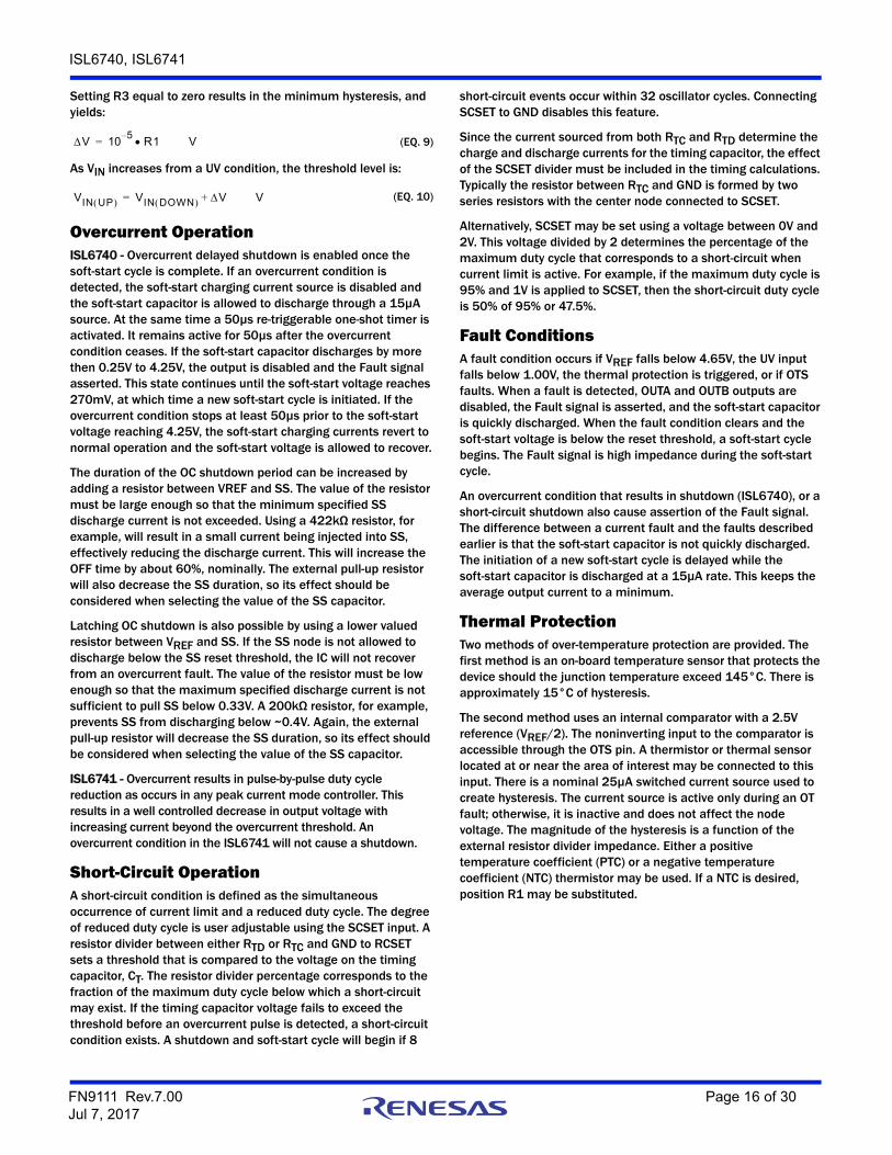
OTS - The noninverting input to the over-temperature shutdown comparator. The signal input at this pin is compared to an internal threshold of VREF/2. If the voltage at this pin exceeds the threshold, the Fault signal is asserted and the outputs are disabled until the condition clears. There is a nominal 25µA switched current source used for hysteresis. The amount of hysteresis is adjustable by varying the source impedance of the signal into this pin.
OTS may be used to monitor parameters other than temperature, such as voltage. Any signal for which a high out-of-bounds monitor is desired may utilize the OTS comparator.
FAULT - The Fault signal is asserted high whenever the outputs, OUTA and OUTB, are disabled. This occurs during an over-temperature fault, an input UV fault, a VREF UV fault, or during an overcurrent (ISL6740) or short-circuit shutdown fault. Fault can be used to disable synchronous rectifiers whenever the outputs are disabled.
Fault is a three-state output and is high impedance during the soft-start cycle. Adding a pull-up resistor to VREF or a pull-down resistor to ground determines the state of Fault during soft-start. This feature allows the designer to use the Fault signal to enable or disable output synchronous rectifiers during soft-start.
UV - Undervoltage monitor input pin. A resistor divider between the input source voltage and GND sets the undervoltage lock out threshold. The signal is compared to an internal 1.00V reference to detect an undervoltage or inhibit condition.
CS - This is the input to the current sense comparator(s). The IC has the PWM comparator for peak current mode control (ISL6741) and an overcurrent protection comparator. The overcurrent comparator threshold is set at 0.600V nominal.
The CS pin is shorted to GND at the end of each switching cycle. Depending on the current sensing source impedance, a series input resistor may be required due to the delay between the internal clock and the external power switch. This delay may allow an overlap such that the CS signal may be discharged while the current signal is still active. If the current sense source is low impedance, it will cause increased power dissipation.
ISL6740 - Exceeding the overcurrent threshold will start a delayed shutdown sequence. Once an overcurrent condition is detected, the soft-start charge current source is disabled. The soft-start capacitor begins discharging through a 25µA current source, and if it discharges to less than 4.25V (sustained overcurrent threshold), a shutdown condition occurs and the OUTA and OUTB outputs are forced low. When the soft-start voltage reaches 0.27V (reset threshold) a soft-start cycle begins.
An overcurrent condition must be absent for 50µs before the delayed shutdown control resets. If the overcurrent condition ceases, and an additional 50µs period elapses before the shutdown threshold is reached, no shutdown occurs. The SS charging current is re-enabled and the soft-start voltage is allowed to recover.
ISL6741 - The ISL6741 current mode controller does not shut down due to an overcurrent condition. The pulse-by-pulse current limit characteristic of peak current mode control limits the output current to acceptable levels.
GND - Reference and power ground for all functions on this device. Due to high peak currents and high frequency operation, a low impedance layout is necessary. Ground planes and short traces are highly recommended.
OUTA and OUTB - Alternate half cycle output stages. Each output is capable of 0.5A peak currents for driving logic level power MOSFETs or MOSFET drivers. Each output provides very low impedance to overshoot and undershoot.
VREF - The 5.00V reference voltage output. +1%/-2% tolerance over line, load and operating temperature. Bypass to GND with a 0.047µF to 2.2µF ceramic capacitor. Capacitors outside of this range may cause oscillation.
SS - Connect the soft-start timing capacitor between this pin and GND to control the duration of soft-start. The value of the capacitor determines the rate of increase of the duty cycle during start-up, controls the overcurrent shutdown delay (ISL6740), and the overcurrent and short-circuit hiccup restart period.
SCSET - Sets the duty cycle threshold that corresponds to a short-circuit condition. A resistive divider between RTC and GND or RTD and GND, or a voltage between 0V and 2V may be used to adjust the SCSET threshold. If using a resistor divider from either RTC or RTD, the impedance to GND affects the oscillator timing and should be considered when determining the oscillator timing components. Connecting SCSET to GND disables short-circuit shutdown and hiccup.
Functional DescriptionFeaturesThe ISL6740, ISL6741 PWMs are an excellent choice for low cost bridge and push-pull topologies for applications requiring accurate duty cycle and dead time control. With its many protection and control features, a highly flexible design with minimal external components is possible. Among its many features are current mode control (ISL6741), adjustable soft-start, overcurrent protection, thermal protection, bidirectional synchronization, fault indication and adjustable frequency.
OscillatorThe ISL6740, ISL6741 have an oscillator with a programmable frequency range to 2MHz, which can be programmed with two resistors and capacitor. The use of three timing elements, RTC, RTD, and CT allow great flexibility and precision when setting the oscillator frequency.
The switching period may be considered the sum of the timing capacitor charge and discharge durations. The charge duration is determined by RTC and CT. The discharge duration is determined by RTD and CT.
tC 0.5 RTC CT S (EQ. 2)
tD 0.02 RTD CT S (EQ. 3)
tSW tC tD+1
fSW----------= = S (EQ. 4)
FN9111 Rev.7.00 Page 14 of 30Jul 7, 2017
ISL6740, ISL6741
where tC and tD are the charge and discharge times, respectively, tSW is the oscillator free running period, and f is the oscillator frequency. One output switching cycle requires two oscillator cycles. The actual times will be slightly longer than calculated due to internal propagation delays of approximately 10ns/transition. This delay adds directly to the switching duration, but also causes overshoot of the timing capacitor peak and valley voltage thresholds, effectively increasing the peak-to-peak voltage on the timing capacitor. Additionally, if very low charge and discharge currents are used, there will be increased error due to the input impedance at the CT pin.
The maximum duty cycle, D, and percent Dead Time, (TD), can be calculated from:
Implementing SynchronizationThe oscillator can be synchronized to an external clock applied to the SYNC pin or by connecting the SYNC pins of multiple ICs together. If an external master clock signal is used, the free running frequency of the oscillator should be ~10% slower than the desired synchronous frequency. The external master clock signal should have a pulse width greater than 20ns. The SYNC circuitry will not respond to an external signal during the first 60% of the oscillator switching cycle. Self-synchronization is not recommended for oscillator frequencies above 900kHz. For higher switching frequencies, an external clock with a pulse width less than one-half of the oscillator period must be used.
The SYNC input is edge triggered and its duration does not affect oscillator operation. However, the dead time is affected by the SYNC frequency. A higher frequency signal applied to the SYNC input will shorten the dead time. The shortened dead time is the result of the timing capacitor charge cycle being prematurely terminated by the external SYNC pulse. Consequently, the timing capacitor is not fully charged when the discharge cycle begins. This effect is only a concern when an external master clock is used, or if units with different operating frequencies are paralleled.
Soft-Start OperationThe ISL6740, ISL6741 feature a soft-start using an external capacitor in conjunction with an internal current source. Soft-start reduces stresses and surge currents during start-up.
Upon start-up, the soft-start circuitry clamps the error voltage input (VERROR pin) indirectly to a value equal to the soft-start voltage. The soft-start clamp does not actually clamp the error voltage input as is done in many implementations. Rather the PWM comparator has two inverting inputs such that the lower voltage is in control.
The output pulse width increases as the soft-start capacitor voltage increases. This has the effect of increasing the duty cycle from zero to the regulation pulse width during the soft-start period. When the soft-start voltage exceeds the error voltage, soft-start is completed. Soft-start occurs during start-up, after recovery from a Fault condition or overcurrent/short-circuit shutdown. The soft-start voltage is clamped to 4.5V.
The Fault signal output is high impedance during the soft-start cycle. A pull-up resistor to VREF or a pull-down resistor to ground should be added to achieve the desired state of Fault during soft-start.
Gate DriveThe ISL6740, ISL6741 are capable of sourcing and sinking 0.5A peak current, but are primarily intended to be used in conjunction with a MOSFET driver due to the 5V drive level. To limit the peak current through the IC, an external resistor may be placed between the totem-pole output of the IC (OUTA or OUTB pin) and the gate of the MOSFET. This small series resistor also damps any oscillations caused by the resonant tank of the parasitic inductances in the traces of the board and the FET’s input capacitance.
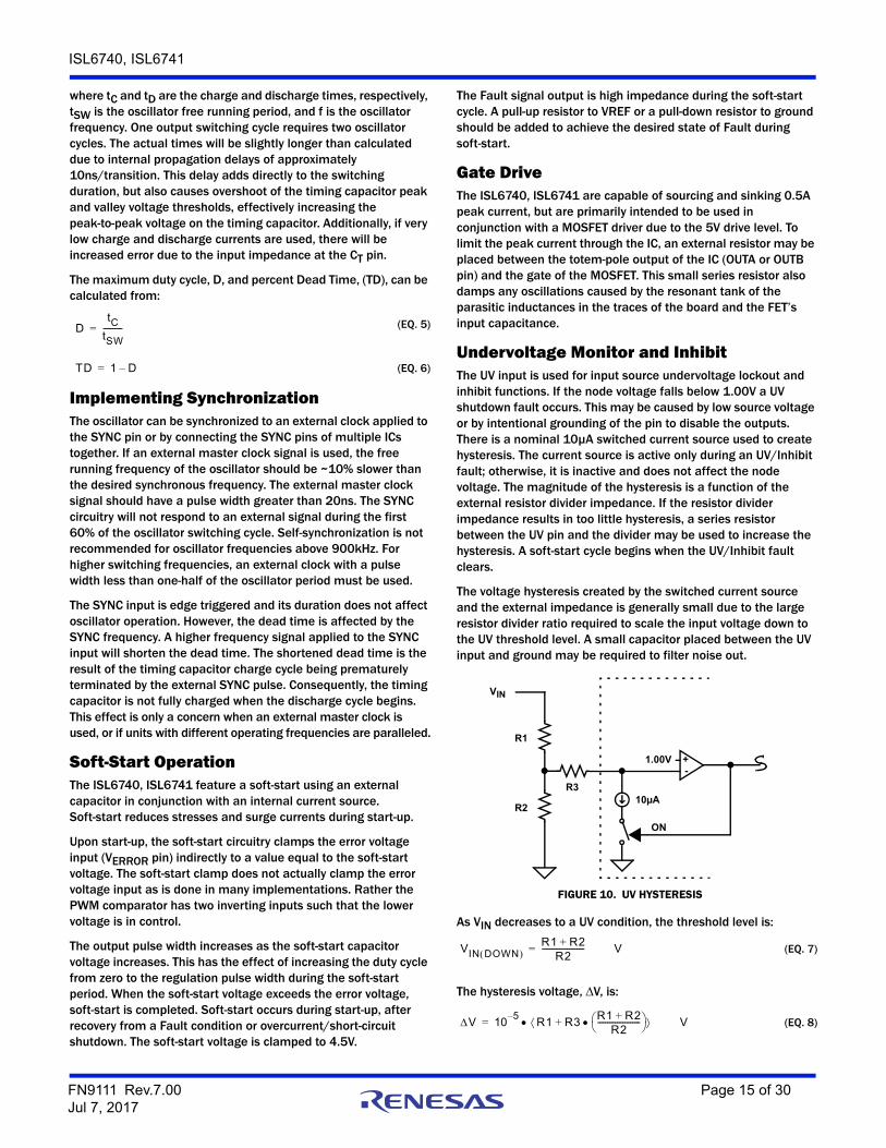
Undervoltage Monitor and InhibitThe UV input is used for input source undervoltage lockout and inhibit functions. If the node voltage falls below 1.00V a UV shutdown fault occurs. This may be caused by low source voltage or by intentional grounding of the pin to disable the outputs. There is a nominal 10µA switched current source used to create hysteresis. The current source is active only during an UV/Inhibit fault; otherwise, it is inactive and does not affect the node voltage. The magnitude of the hysteresis is a function of the external resistor divider impedance. If the resistor divider impedance results in too little hysteresis, a series resistor between the UV pin and the divider may be used to increase the hysteresis. A soft-start cycle begins when the UV/Inhibit fault clears.
The voltage hysteresis created by the switched current source and the external impedance is generally small due to the large resistor divider ratio required to scale the input voltage down to the UV threshold level. A small capacitor placed between the UV input and ground may be required to filter noise out.
As VIN decreases to a UV condition, the threshold level is:
The hysteresis voltage, V, is:
DtC
tSW----------= (EQ. 5)
TD 1 D–= (EQ. 6)
FIGURE 10. UV HYSTERESIS
VIN
R1
R2
R3
1.00V
10µA
ON
+-
VIN DOWN R1 R2+
R2----------------------= V (EQ. 7)
V 105–
R1 R3R1 R2+
R2---------------------- + = V (EQ. 8)
FN9111 Rev.7.00 Page 15 of 30Jul 7, 2017
ISL6740, ISL6741
Setting R3 equal to zero results in the minimum hysteresis, and yields:
As VIN increases from a UV condition, the threshold level is:
Overcurrent OperationISL6740 - Overcurrent delayed shutdown is enabled once the soft-start cycle is complete. If an overcurrent condition is detected, the soft-start charging current source is disabled and the soft-start capacitor is allowed to discharge through a 15µA source. At the same time a 50µs re-triggerable one-shot timer is activated. It remains active for 50µs after the overcurrent condition ceases. If the soft-start capacitor discharges by more then 0.25V to 4.25V, the output is disabled and the Fault signal asserted. This state continues until the soft-start voltage reaches 270mV, at which time a new soft-start cycle is initiated. If the overcurrent condition stops at least 50µs prior to the soft-start voltage reaching 4.25V, the soft-start charging currents revert to normal operation and the soft-start voltage is allowed to recover.
The duration of the OC shutdown period can be increased by adding a resistor between VREF and SS. The value of the resistor must be large enough so that the minimum specified SS discharge current is not exceeded. Using a 422kΩ resistor, for example, will result in a small current being injected into SS, effectively reducing the discharge current. This will increase the OFF time by about 60%, nominally. The external pull-up resistor will also decrease the SS duration, so its effect should be considered when selecting the value of the SS capacitor.
Latching OC shutdown is also possible by using a lower valued resistor between VREF and SS. If the SS node is not allowed to discharge below the SS reset threshold, the IC will not recover from an overcurrent fault. The value of the resistor must be low enough so that the maximum specified discharge current is not sufficient to pull SS below 0.33V. A 200kΩ resistor, for example, prevents SS from discharging below ~0.4V. Again, the external pull-up resistor will decrease the SS duration, so its effect should be considered when selecting the value of the SS capacitor.
ISL6741 - Overcurrent results in pulse-by-pulse duty cycle reduction as occurs in any peak current mode controller. This results in a well controlled decrease in output voltage with increasing current beyond the overcurrent threshold. An overcurrent condition in the ISL6741 will not cause a shutdown.
Short-Circuit OperationA short-circuit condition is defined as the simultaneous occurrence of current limit and a reduced duty cycle. The degree of reduced duty cycle is user adjustable using the SCSET input. A resistor divider between either RTD or RTC and GND to RCSET sets a threshold that is compared to the voltage on the timing capacitor, CT. The resistor divider percentage corresponds to the fraction of the maximum duty cycle below which a short-circuit may exist. If the timing capacitor voltage fails to exceed the threshold before an overcurrent pulse is detected, a short-circuit condition exists. A shutdown and soft-start cycle will begin if 8
short-circuit events occur within 32 oscillator cycles. Connecting SCSET to GND disables this feature.
Since the current sourced from both RTC and RTD determine the charge and discharge currents for the timing capacitor, the effect of the SCSET divider must be included in the timing calculations. Typically the resistor between RTC and GND is formed by two series resistors with the center node connected to SCSET.
Alternatively, SCSET may be set using a voltage between 0V and 2V. This voltage divided by 2 determines the percentage of the maximum duty cycle that corresponds to a short-circuit when current limit is active. For example, if the maximum duty cycle is 95% and 1V is applied to SCSET, then the short-circuit duty cycle is 50% of 95% or 47.5%.
Fault ConditionsA fault condition occurs if VREF falls below 4.65V, the UV input falls below 1.00V, the thermal protection is triggered, or if OTS faults. When a fault is detected, OUTA and OUTB outputs are disabled, the Fault signal is asserted, and the soft-start capacitor is quickly discharged. When the fault condition clears and the soft-start voltage is below the reset threshold, a soft-start cycle begins. The Fault signal is high impedance during the soft-start cycle.
An overcurrent condition that results in shutdown (ISL6740), or a short-circuit shutdown also cause assertion of the Fault signal. The difference between a current fault and the faults described earlier is that the soft-start capacitor is not quickly discharged. The initiation of a new soft-start cycle is delayed while the soft-start capacitor is discharged at a 15µA rate. This keeps the average output current to a minimum.
Thermal ProtectionTwo methods of over-temperature protection are provided. The first method is an on-board temperature sensor that protects the device should the junction temperature exceed 145°C. There is approximately 15°C of hysteresis.
The second method uses an internal comparator with a 2.5V reference (VREF/2). The noninverting input to the comparator is accessible through the OTS pin. A thermistor or thermal sensor located at or near the area of interest may be connected to this input. There is a nominal 25µA switched current source used to create hysteresis. The current source is active only during an OT fault; otherwise, it is inactive and does not affect the node voltage. The magnitude of the hysteresis is a function of the external resistor divider impedance. Either a positive temperature coefficient (PTC) or a negative temperature coefficient (NTC) thermistor may be used. If a NTC is desired, position R1 may be substituted.
V 105–
R1= V (EQ. 9)
VIN UP VIN DOWN V+= V (EQ. 10)
FN9111 Rev.7.00 Page 16 of 30Jul 7, 2017
ISL6740, ISL6741
If a PTC is desired, then position R2 may be substituted. The threshold with increasing temperature is set by making the fixed resistance equal in value to the thermistor resistance at the desired trip temperature.
VTH= 2.5V and R1 = R2 (HOT)
To determine the value of the hysteresis resistor, R3, select the value of thermistor resistance that corresponds to the desired reset temperature.
If the hysteresis resistor, R3, is not desired, the value of the thermistor resistance at the reset temperature can be determined from:
The OTS comparator may also be used to monitor signals other than suggested above. It may also be used to monitor any voltage signal for which an excess requires a response as described above. Input or output voltage monitoring are examples of this.
Ground Plane RequirementsCareful layout is essential for satisfactory operation of the device. A good ground plane must be employed. VDD should be bypassed directly to GND with good high frequency capacitance.
Typical ApplicationThe Typical Application Schematic on page 5 features the ISL6740 in an unregulated half-bridge DC/DC converter configuration, often referred to as a DC transformer or bus regulator. The ISL6740EVAL1 demonstration unit implements this design and is available for evaluation.
The input voltage range is 48 ±10% VDC. The output is a nominal 12V when the input voltage is at 48V. Since this is an unregulated topology, the output voltage will vary proportionately with input voltage. The load regulation is a function of resistance between the source and the converter output. The output is rated at 8A.
Circuit Element DescriptionsThe converter design may be broken down into the following functional blocks:
Input Filtering: L1, C1, R1
Half-Bridge Capacitors: C2, C3
Isolation Transformer: T1
Primary Snubber: C13, R10
Start Bias Regulator: CR3, R2, R7, C6, Q5, D1
Supply Bypass Components: R3, C15, C4, C5
Main MOSFET Power Switch: QH, QL
Current Sense Network: T2, CR1, CR2, R5, R6, R11, C10, C14
Control Circuit: U3, RT1, R14, R19, R13, R15, R17, R18, C16, C18, C17
Output Rectification and Filtering: QR1, QR2, QR3, QR4, L2, C9, C8
Secondary Snubber: R8, R9, C11, C12
FET Driver: U1
ZVS Resonant Delay (Optional): L3, C7
Design CriteriaThe following design requirements were selected:
Switching Frequency, fSW: 235kHz
VIN: 48 ±10% V
VOUT: 12V (nominal) at IOUT = 8A
POUT: 100W
Efficiency: 95%
Ripple: 1%
Transformer DesignThe design of a transformer for a half-bridge application is a straight forward affair, although iterative. It is a process of many compromises, and even experienced designers will produce different designs when presented with identical requirements. The iterative design process is not presented here for clarity.
The abbreviated design process follows:
• Select a core geometry suitable for the application. Constraints of height, footprint, mounting preference, and operating environment will affect the choice.
• Determine the turns ratio.
• Select suitable core material(s).
• Select maximum flux density desired for operation.
• Select core size. Core size will be dictated by the capability of the core structure to store the required energy, the number of turns that have to be wound, and the wire gauge needed. Often the window area (the space used for the windings) and power loss determine the final core size.
• Determine maximum desired flux density. Depending on the frequency of operation, the core material selected, and the
FIGURE 11. OTS HYSTERESIS
VREF
R1
R2
R3 VREF/2
25µA
ON
+-
VREF
R310
5R1 R2– R1 R2–
R1 R2+---------------------------------------------------------------------- = (EQ. 11)
R12.5 R2
2.5 105–
R2–----------------------------------------= NTC (EQ. 12)
R22.5 R1
2.5 105–
R1+-----------------------------------------= PTC (EQ. 13)
FN9111 Rev.7.00 Page 17 of 30Jul 7, 2017
ISL6740, ISL6741
operating environment, the allowed flux density must be determined. The decision of what flux density to allow is often difficult to determine initially. Usually the highest flux density that produces an acceptable design is used, but often the winding geometry dictates a larger core than is indicated based on flux density alone.
• Determine the number of primary turns.
• Select the wire gauge for each winding.
• Determine winding order and insulation requirements.
• Verify the design.
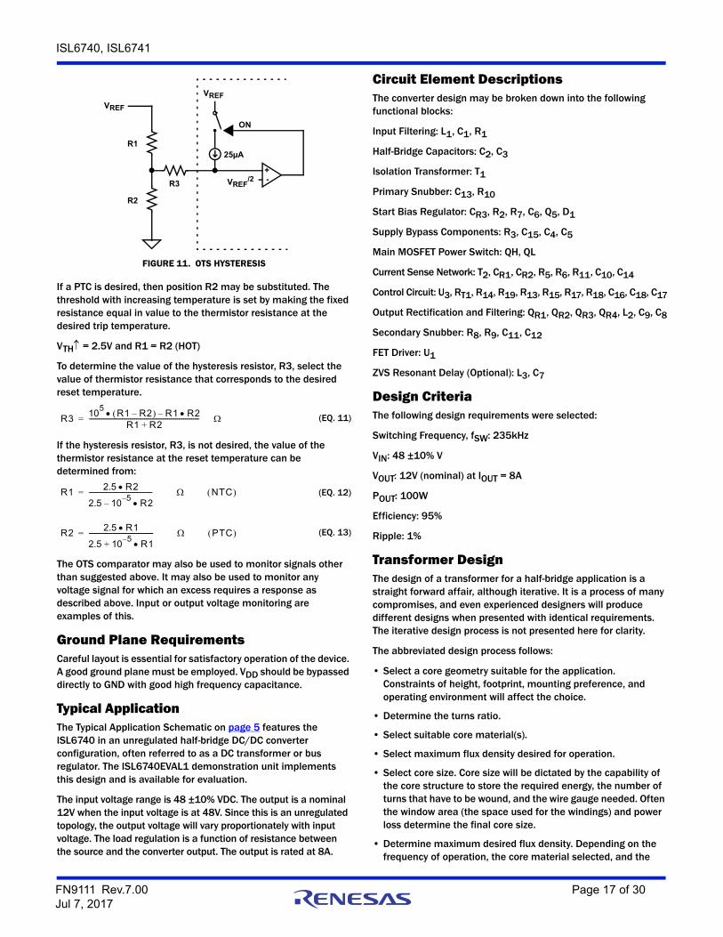
For this application we have selected a planar structure to achieve a low profile design. A PQ style core was selected because of its round center leg cross section, but there are many suitable core styles available.
Since the converter is operating open loop at nearly 100% duty cycle, the turns ratio, N, is simply the ratio of the input voltage to the output voltage divided by 2.
The factor of 2 divisor is due to the half-bridge topology. Only half of the input voltage is applied to the primary of the transformer.
A PC44HPQ20/6 “E-Core” plus a PC44PQ20/3 “I-Core” from TDK were selected for the transformer core. The ferrite material is PC44.
The core parameter of concern for flux density is the effective core cross sectional area, Ae. For the PQ core pieces selected:
Ae = 0.62cm2 or 6.2e -5m2
Using Faraday’s Law, V = N d/dt, the number of primary turns can be determined once the maximum flux density is set. An acceptable Bmax is ultimately determined by the allowable power dissipation in the ferrite material and is influenced by the lossiness of the core, core geometry, operating ambient temperature, and air flow. The TDK datasheet for PC44 material indicates a core loss factor of ~400mW/cm3 with a ±2000 gauss 100kHz sinusoidal excitation. The application uses a 235kHz square wave excitation, so no direct comparison between the application and the data can be made. Interpolation of the data is required. The core volume is approximately 1.6cm3, so the estimated core loss is:
1.28W of dissipation is significant for a core of this size. Reducing the flux density to 1200 gauss will reduce the dissipation by about the same percentage, or 40%. Ultimately, evaluation of the transformer’s performance in the application will determine what is acceptable.
From Faraday’s Law and using 1200 gauss peak flux density (B = 2400 gauss or 0.24 tesla.)
Rounding up yields 4 turns for the primary winding. The peak flux density using 4 turns is ~1100 gauss. From Equation 16, the number of secondary turns is 2.
The volts/turn for this design ranges from 5.4V at VIN = 43V to 6.6V at VIN = 53V. Therefore, the synchronous rectifier (SR) windings may be set at 1 turn each with proper FET selection. Selecting 2 turns for the synchronous rectifier windings would also be acceptable, but the gate drive losses would increase.
The next step is to determine the equivalent wire gauge for the planar structure. Since each secondary winding conducts for only 50% of the period, the RMS current is:
Where D is the duty cycle. Since an FR-4 PWB planar winding structure was selected, the width of the copper traces is limited by the window area width, and the number of layers is limited by the window area height. The PQ core selected has a usable window area width of 0.165 inches. Allowing one turn per layer and 0.020 inches clearance at the edges allows a maximum trace width of 0.125 inches. Using 100 circular mils (c.m.)/A as a guideline for current density, and from Equation 17, 707c.m. are required for each of the secondary windings (a circular mil is the area of a circle 0.001 inches in diameter). Converting c.m. to square mils yields 555mils2 (0.785 sq. mils/c.m.). Dividing by the trace width results in a copper thickness of 4.44 mils (0.112mm). Using 1.3 mils/oz. of copper requires a copper weight of 3.4oz. For reasons of cost, 3oz. copper was selected.
One layer of each secondary winding also contains the synchronous rectifier winding. For this layer the secondary trace width is reduced by 0.025 inches to 0.100 inches (0.015 inches for the SR winding trace width and 0.010 inches spacing between the SR winding and the secondary winding).
The choice of copper weight may be validated by calculating the DC copper losses of the secondary winding as follows. Ignoring the terminal and lead-in resistance, the resistance of each layer of the secondary may be approximated using Equation 18.
Where:
R = Winding resistance = Resistivity of copper = 669e-9Ω-inches at 20°Ct = Thickness of the copper (3oz.) = 3.9e-3 inchesr2 = Outside radius of the copper trace = 0.324 or 0.299 inchesr1 = Inside radius of the copper trace = 0.199 inches
FIGURE 12. TRANSFORMER SCHEMATIC
nP
nSR
nS
nS
nSR
NVIN
VOUT 2------------------------- 48
12 2--------------- 2= = = (EQ. 14)
PlossmW
cm3
----------- cm3 fact
fmeas--------------- 0.4 1.6
200kHz100kHz--------------------- 1.28= = W
(EQ. 15)
NVIN TON
2 Ae B------------------------------ 53 2 10
6–
2 6.2 105–
0.24----------------------------------------------------- 3.56= = = turns
(EQ. 16)
IRMS IOUT D 10 0.5 7.07= = = A (EQ. 17)
R2
tr2r1-----
ln
------------------------= (EQ. 18)
FN9111 Rev.7.00 Page 18 of 30Jul 7, 2017
ISL6740, ISL6741
The winding without the SR winding on the same layer has a DC resistance of 2.21mΩ. The winding that shares the layer with the SR winding has a DC resistance of 2.65mΩ. With the secondary configured as a 4 turn center tapped winding (2 turns each side of the tap), the total DC power loss for the secondary at +20°C is 486mW.
The primary windings have an RMS current of approximately 5A (IOUT x NS/NP at ~ 100% duty cycle). The primary is configured as 2 layers, 2 turns per layer to minimize the winding stack height. Allowing 0.020 inches edge clearance and 0.010 inches between turns yields a trace width of 0.0575 inches. Ignoring the terminal and lead-in resistance, and using Equation 18, the inner trace has a resistance of 4.25mΩ, and the outer trace has a resistance of 5.52mΩ. The resistance of the primary then is 19.5mΩ at +20°C. The total DC power loss for the secondary at +20°C is 489mW.
Improved efficiency and thermal performance could be achieved by selecting heavier copper weight for the windings. Evaluation in the application will determine its need.
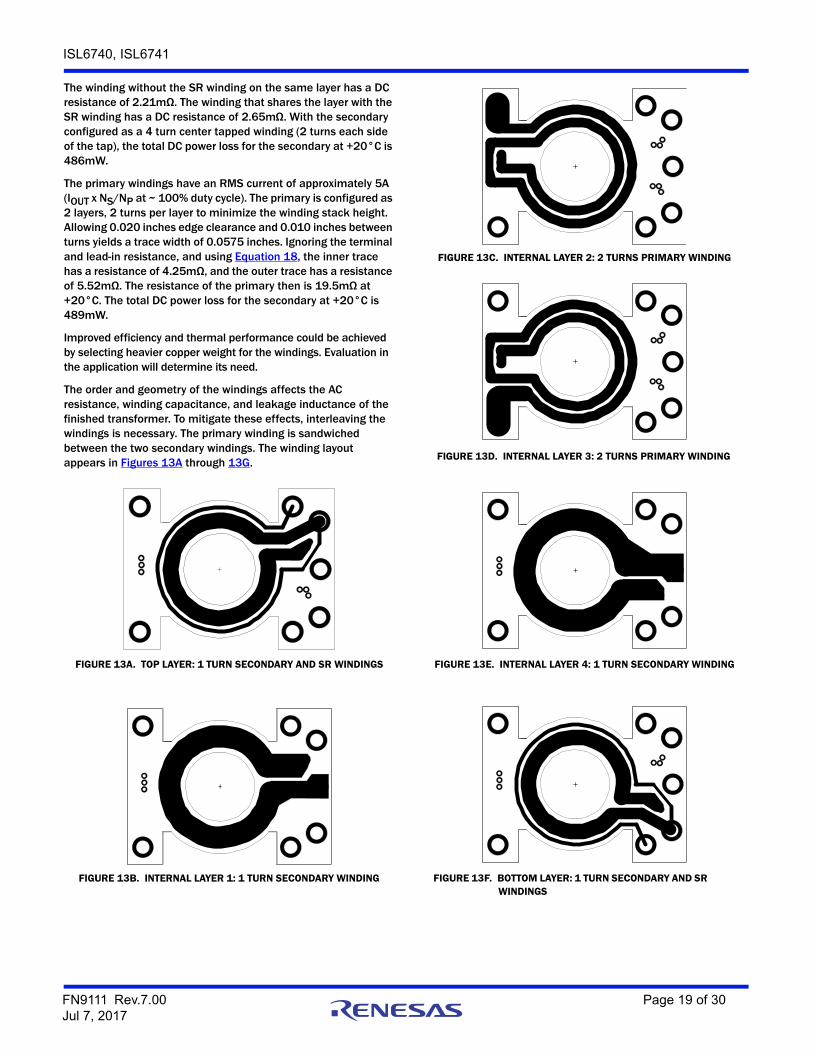
The order and geometry of the windings affects the AC resistance, winding capacitance, and leakage inductance of the finished transformer. To mitigate these effects, interleaving the windings is necessary. The primary winding is sandwiched between the two secondary windings. The winding layout appears in Figures 13A through 13G.
FIGURE 13A. TOP LAYER: 1 TURN SECONDARY AND SR WINDINGS
FIGURE 13B. INTERNAL LAYER 1: 1 TURN SECONDARY WINDING
FIGURE 13C. INTERNAL LAYER 2: 2 TURNS PRIMARY WINDING
FIGURE 13D. INTERNAL LAYER 3: 2 TURNS PRIMARY WINDING
FIGURE 13E. INTERNAL LAYER 4: 1 TURN SECONDARY WINDING
FIGURE 13F. BOTTOM LAYER: 1 TURN SECONDARY AND SR WINDINGS
FN9111 Rev.7.00 Page 19 of 30Jul 7, 2017
ISL6740, ISL6741
MOSFET SelectionThe criteria for selection of the primary side half-bridge FETs and the secondary side synchronous rectifier FETs is largely based on the current and voltage rating of the device. However, the FET drain-source capacitance and gate charge cannot be ignored.
The Zero Voltage Switch (ZVS) transition timing is dependent on the transformer’s leakage inductance and the capacitance at the node between the upper FET source and the lower FET drain. The node capacitance is comprised of the drain-source capacitance of the FETs and the transformer parasitic capacitance. The leakage inductance and capacitance form an LC resonant tank circuit which determines the duration of the transition. The amount of energy stored in the LC tank circuit determines the transition voltage amplitude. If the leakage inductance energy is too low, ZVS operation is not possible and near or partial ZVS operation occurs. As the leakage energy increases, the voltage amplitude increases until it is clamped by the FET body diode to ground or VIN, depending on which FET conducts. When the leakage energy exceeds the minimum required for ZVS operation, the voltage is clamped until the energy is transferred. This behavior increases the time window for ZVS operation. This behavior is not without consequences, however. The transition time and the period of time during which the voltage is clamped reduces the effective duty cycle.
The gate charge affects the switching speed of the FETs. Higher gate charge translates into higher drive requirements and/or slower switching speeds. The energy required to drive the gates is dissipated as heat.
The maximum input voltage, VIN, plus transient voltage, determines the voltage rating required. With a maximum input voltage of 53V for this application, and if we allow a 10% adder for transients, a voltage rating of 60V or higher will suffice.
The RMS current through each primary side FET can be determined from Equation 17, substituting 5A of primary current for IOUT. The result is 3.5A RMS. Fairchild FDS3672 FETs, rated at 100V and 7.5A (rDS(ON) = 22mΩ), were selected for the half-bridge switches.
The synchronous rectifier FETs must withstand approximately one half of the input voltage assuming no switching transients are present. This suggests a device capable of withstanding at least 30V is required. Empirical testing in the circuit revealed
switching transients of 20V were present across the device indicating a rating of at least 60V is required.
The RMS current rating of 7.07A for each SR FET requires a low rDS(ON) to minimize conduction losses, which is difficult to find in a 60V device. It was decided to use two devices in parallel to simplify the thermal design. Two Fairchild FDS5670 devices are used in parallel for a total of four SR FETs. The FDS5670 is rated at 60V and 10A (rDS(ON) = 14mΩ).
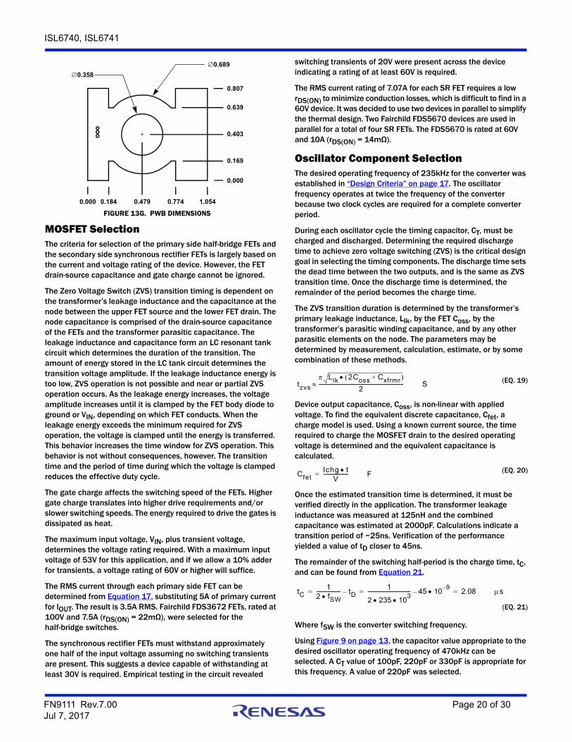
Oscillator Component SelectionThe desired operating frequency of 235kHz for the converter was established in “Design Criteria” on page 17. The oscillator frequency operates at twice the frequency of the converter because two clock cycles are required for a complete converter period.
During each oscillator cycle the timing capacitor, CT, must be charged and discharged. Determining the required discharge time to achieve zero voltage switching (ZVS) is the critical design goal in selecting the timing components. The discharge time sets the dead time between the two outputs, and is the same as ZVS transition time. Once the discharge time is determined, the remainder of the period becomes the charge time.
The ZVS transition duration is determined by the transformer’s primary leakage inductance, Llk, by the FET Coss, by the transformer’s parasitic winding capacitance, and by any other parasitic elements on the node. The parameters may be determined by measurement, calculation, estimate, or by some combination of these methods.
Device output capacitance, Coss, is non-linear with applied voltage. To find the equivalent discrete capacitance, Cfet, a charge model is used. Using a known current source, the time required to charge the MOSFET drain to the desired operating voltage is determined and the equivalent capacitance is calculated.
Once the estimated transition time is determined, it must be verified directly in the application. The transformer leakage inductance was measured at 125nH and the combined capacitance was estimated at 2000pF. Calculations indicate a transition period of ~25ns. Verification of the performance yielded a value of tD closer to 45ns.
The remainder of the switching half-period is the charge time, tC, and can be found from Equation 21.
Where fSW is the converter switching frequency.
Using Figure 9 on page 13, the capacitor value appropriate to the desired oscillator operating frequency of 470kHz can be selected. A CT value of 100pF, 220pF or 330pF is appropriate for this frequency. A value of 220pF was selected.
FIGURE 13G. PWB DIMENSIONS
0.689
0.807
0.639
0.403
0.169
0.000
1.0540.7740.4790.1840.000
0.358
tzvs
Llk 2Coss Cxfrmr+
2-------------------------------------------------------------------- S (EQ. 19)
CfetIchg t
V--------------------= F (EQ. 20)
tC1
2 fSW------------------- tD–
1
2 235 103
---------------------------------- 45 109–– 2.08= = = s
(EQ. 21)
FN9111 Rev.7.00 Page 20 of 30Jul 7, 2017
ISL6740, ISL6741
To obtain the proper value for RTD, Equation 3 on page 14 is used. Since there is a 10ns propagation delay in the oscillator circuit, it must be included in the calculation. The value of RTD selected is 8.06kΩ.
A similar procedure is used to determine the value of RTC using Equation 2 on page 14. The value of RTC selected is the series combination of 17.4kΩ and 1.27kΩ. See section “Overcurrent Component Selection” on page 21 for further explanation.
Output Filter DesignThe output filter inductor and capacitor selection is simple and straightforward. Under steady state operating conditions the voltage across the inductor is very small due to the large duty cycle. Voltage is applied across the inductor only during the switch transition time, about 45ns in this application. Ignoring the voltage drop across the SR FETs, the voltage across the inductor during the ON time with VIN = 48V is:
Where:
VL is the inductor voltageVS is the voltage across the secondary windingVOUT is the output voltage
If we allow a current ramp, I, of 5% of the rated output current, the minimum inductance required is:
An inductor value of 1.4µH, rated for 18A was selected.
With a maximum input voltage of 53V, the maximum output voltage is about 13V. The closest higher voltage rated capacitor is 16V. Under steady state operating conditions the ripple current in the capacitor is small, so it would seem appropriate to have a low ripple current rated capacitor. However, a high rated ripple current capacitor was selected based on the nature of the intended load, multiple buck regulators. To minimize the output impedance of the filter, a Sanyo OSCON 16SH150M capacitor in parallel with a 22µF ceramic capacitor were selected.
Overcurrent Component SelectionThere are two circuit areas to consider when selecting the components for overcurrent protection, current limit and short-circuit shutdown. The current limit threshold is fixed at 0.6V while the short-circuit threshold is set to a fraction of the duty cycle the designer wishes to define as a short-circuit.
The current level that corresponds to the overcurrent threshold must be chosen to allow for the dynamic behavior of an open loop converter. In particular, the low inductor ripple current under steady state operation increases significantly as the duty cycle decreases.
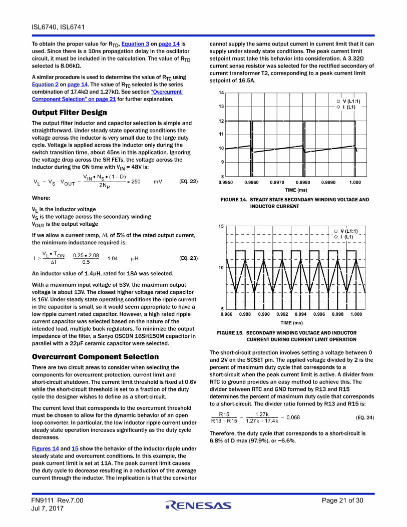
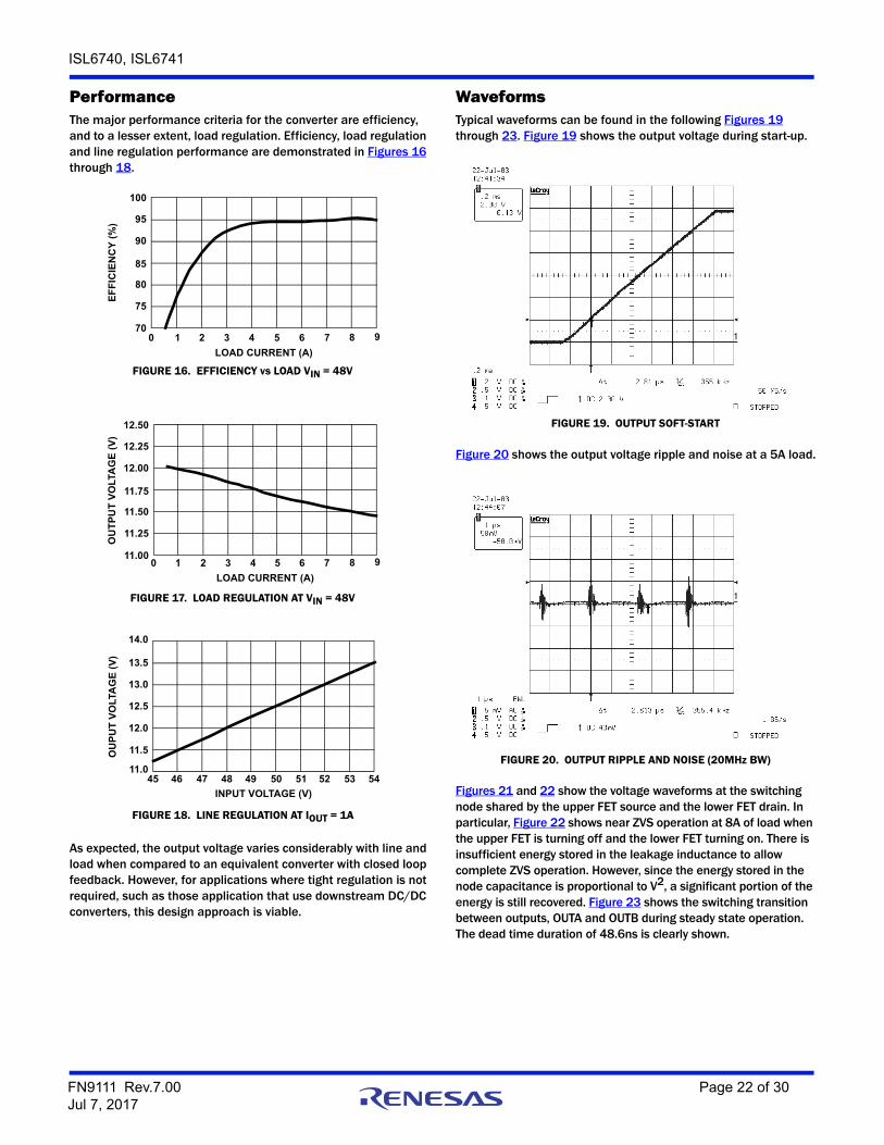
Figures 14 and 15 show the behavior of the inductor ripple under steady state and overcurrent conditions. In this example, the peak current limit is set at 11A. The peak current limit causes the duty cycle to decrease resulting in a reduction of the average current through the inductor. The implication is that the converter
cannot supply the same output current in current limit that it can supply under steady state conditions. The peak current limit setpoint must take this behavior into consideration. A 3.32Ω current sense resistor was selected for the rectified secondary of current transformer T2, corresponding to a peak current limit setpoint of 16.5A.
The short-circuit protection involves setting a voltage between 0 and 2V on the SCSET pin. The applied voltage divided by 2 is the percent of maximum duty cycle that corresponds to a short-circuit when the peak current limit is active. A divider from RTC to ground provides an easy method to achieve this. The divider between RTC and GND formed by R13 and R15 determines the percent of maximum duty cycle that corresponds to a short-circuit. The divider ratio formed by R13 and R15 is:
Therefore, the duty cycle that corresponds to a short-circuit is 6.8% of D max (97.9%), or ~6.6%.
VL VS VOUT–VIN NS 1 D–
2NP------------------------------------------------ 250= = mV (EQ. 22)
LVL TON
I------------------------- 0.25 2.08
0.5----------------------------- 1.04= = H (EQ. 23)
FIGURE 14. STEADY STATE SECONDARY WINDING VOLTAGE AND INDUCTOR CURRENT
14
13
12
11
10
9
80.9950 0.9960 0.9970 0.9980 0.9990 1.000
TIME (ms)
V (L1:1)I (L1)
FIGURE 15. SECONDARY WINDING VOLTAGE AND INDUCTOR CURRENT DURING CURRENT LIMIT OPERATION
0.986 0.988 0.990 0.992 0.994 1.000
TIME (ms)
0.996 0.998
15
10
5
V (L1:1)I (L1)
R15R13 R15+----------------------------- 1.27k
1.27k 17.4k+------------------------------------ 0.068= = (EQ. 24)
FN9111 Rev.7.00 Page 21 of 30Jul 7, 2017
ISL6740, ISL6741
PerformanceThe major performance criteria for the converter are efficiency, and to a lesser extent, load regulation. Efficiency, load regulation and line regulation performance are demonstrated in Figures 16 through 18.
As expected, the output voltage varies considerably with line and load when compared to an equivalent converter with closed loop feedback. However, for applications where tight regulation is not required, such as those application that use downstream DC/DC converters, this design approach is viable.
WaveformsTypical waveforms can be found in the following Figures 19 through 23. Figure 19 shows the output voltage during start-up.
Figure 20 shows the output voltage ripple and noise at a 5A load.
Figures 21 and 22 show the voltage waveforms at the switching node shared by the upper FET source and the lower FET drain. In particular, Figure 22 shows near ZVS operation at 8A of load when the upper FET is turning off and the lower FET turning on. There is insufficient energy stored in the leakage inductance to allow complete ZVS operation. However, since the energy stored in the node capacitance is proportional to V2, a significant portion of the energy is still recovered. Figure 23 shows the switching transition between outputs, OUTA and OUTB during steady state operation. The dead time duration of 48.6ns is clearly shown.
FIGURE 16. EFFICIENCY vs LOAD VIN = 48V
LOAD CURRENT (A)
EF
FIC
IEN
CY
(%
)
100
95
90
85
80
75
700 1 2 3 4 5 6 7 8 9
FIGURE 17. LOAD REGULATION AT VIN = 48V
LOAD CURRENT (A)
OU
TP
UT
VO
LTA
GE
(V
)
12.50
12.25
12.00
11.75
11.50
11.25
11.000 1 2 3 4 5 6 7 8 9
FIGURE 18. LINE REGULATION AT IOUT = 1A
INPUT VOLTAGE (V)
45 46 47 48 49 50 51 52 53 54
14.0
13.5
13.0
12.5
12.0
11.5
11.0
OU
PU
T V
OLT
AG
E (
V)
FIGURE 19. OUTPUT SOFT-START
FIGURE 20. OUTPUT RIPPLE AND NOISE (20MHz BW)
FN9111 Rev.7.00 Page 22 of 30Jul 7, 2017
ISL6740, ISL6741
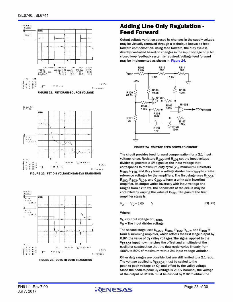
Adding Line Only Regulation - Feed ForwardOutput voltage variation caused by changes in the supply voltage may be virtually removed through a technique known as feed forward compensation. Using feed forward, the duty cycle is directly controlled based on changes in the input voltage only. No closed loop feedback system is required. Voltage feed forward may be implemented as shown in Figure 24.
The circuit provides feed forward compensation for a 2:1 input voltage range. Resistors R100 and R101 set the input voltage divider to generate a 1V signal at the input voltage that corresponds to maximum duty cycle (VIN minimum). Resistors R109, R110, and R111 form a voltage divider from VREF to create reference voltages for the amplifiers. The first stage uses U100A, R102, R103, R104, and C100 to form a unity gain inverting amplifier. Its output varies inversely with input voltage and ranges from 1V to 2V. The bandwidth of the circuit may be controlled by varying the value of C100. The gain of the first amplifier stage is:
Where:
VA = Output voltage of U100AVD = The input divider voltage
The second stage uses U100B, R105, R106, R107, and R108 to form a summing amplifier, which offsets the first stage output by 0.8V (the value of CT valley voltage). The signal applied to the VERROR input now matches the offset and amplitude of the oscillator sawtooth so that the duty cycle varies linearly from 100% to 50% of maximum with a 2:1 input voltage variation.
Other duty ranges are possible, but are still limited to a 2:1 ratio. The voltage applied to VERROR must be scaled to the peak-to-peak voltage on CT, and offset by the valley voltage. Since the peak-to-peak CT voltage is 2.00V nominal, the voltage at the output of U100A must be divided by 2.0V to obtain the
FIGURE 21. FET DRAIN-SOURCE VOLTAGE
FIGURE 22. FET D-S VOLTAGE NEAR-ZVS TRANSITION
FIGURE 23. OUTA TO OUTB TRANSITION
FIGURE 24. VOLTAGE FEED FORWARD CIRCUIT
+-
+-
1.5V 0.8V
R102100k
R1012k
R10069.8k
+VIN
VREF
R1093.48k
R110698
R111806
R104100k
R106100k
R105100k
R107100k
R108100k
R10349.9k
C1001nF
TO VERROR
U100A
U100B
VA VD 3.00+–= V (EQ. 25)
FN9111 Rev.7.00 Page 23 of 30Jul 7, 2017
ISL6740, ISL6741
desired duty cycle. For example, if an 80% duty cycle was required at the minimum operating voltage, the output of U100A must be 1.60V (80% of 2.00V). From (Equation 25), the divider voltage must be set to 1.4V for the input voltage that corresponds to the 80% duty cycle.
It should be noted that the synchronous rectifiers (SRs), being driven from the transformer secondary, are only gated on during the ON time of the primary FETs. Conduction continues through the body diodes during the OFF time when operating in continuous inductor current mode. This mode of operation usually results in significant conduction and switching losses in the SR FETs. These losses may be reduced considerably by either adding Schottky diodes in parallel to the SR FETs or by driving the SR FETs directly with a control signal.
Adding Regulation - Closed Loop FeedbackThe second Typical Application schematic on page 7 adds closed loop feedback with isolation. The ISL6740EVAL2Z demonstration platform implements this design and is available for evaluation. The input voltage range was increased to 36V to 75V, which necessitates a few modifications to the open loop design. The output inductor value was increased to 4.0µH, Schottky rectifier CR4 was added to minimize SR FET body diode conduction, the turns ratio of the main transformer was changed to 4:3, and the synchronous rectifier gate drives were modified. The design process is essentially the same as it was for the unregulated version, so only the feedback control loop design will be discussed.
The major components of the feedback control loop are a programmable shunt regulator and an optocoupler. The opto-coupler is used to transfer the error signal across the isolation barrier. The optocoupler offers a convenient means to cross the isolation barrier, but it adds complexity to the feedback control loop. It adds a pole at about 10kHz and a significant amount of gain variation due the Current Transfer Ratio (CTR). The CTR of the optocoupler varies with initial tolerance, temperature, forward current and age.
A block diagram of the feedback control loop follows in Figure 25.
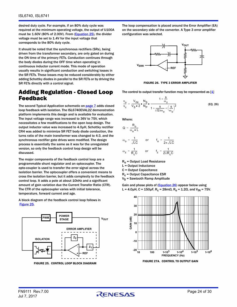
The loop compensation is placed around the Error Amplifier (EA) on the secondary side of the converter. A Type 3 error amplifier configuration was selected.
The control to output transfer function may be represented as [1]
Where:
Ro = Output Load ResistanceL = Output InductanceC = Output CapacitanceRc = Output Capacitance ESRVS = Sawtooth Ramp Amplitude
Gain and phase plots of (Equation 26) appear below usingL = 4.0µH, C = 150µF, Rc = 28mΩ, Ro = 1.2Ω, and VIN = 75V.
FIGURE 25. CONTROL LOOP BLOCK DIAGRAM
PWMPOWERSTAGE
Z1
Z2
REF+
-
ISOLATION
ERROR AMPLIFIER
VOUT
FIGURE 26. TYPE 3 ERROR AMPLIFIER
REF+
-
VOUT
VERR
vovc------
VINVS 2----------------
NSNP--------
1sz------+
1s
Q o----------------- s
o------- 2
+ +
-------------------------------------------------= (EQ. 26)
QRo
o L----------------=
o1
LC------------= or fo
1
2 LC-------------------=
z1
RcC-----------= or fz
12RcC-------------------=
FIGURE 27A. CONTROL TO OUTPUT GAIN
10 100 1•106-20
-10
0
10
20
30
40
FREQUENCY (Hz)
GA
IN (
dB
)
1•1051•1041•103
FN9111 Rev.7.00 Page 24 of 30Jul 7, 2017
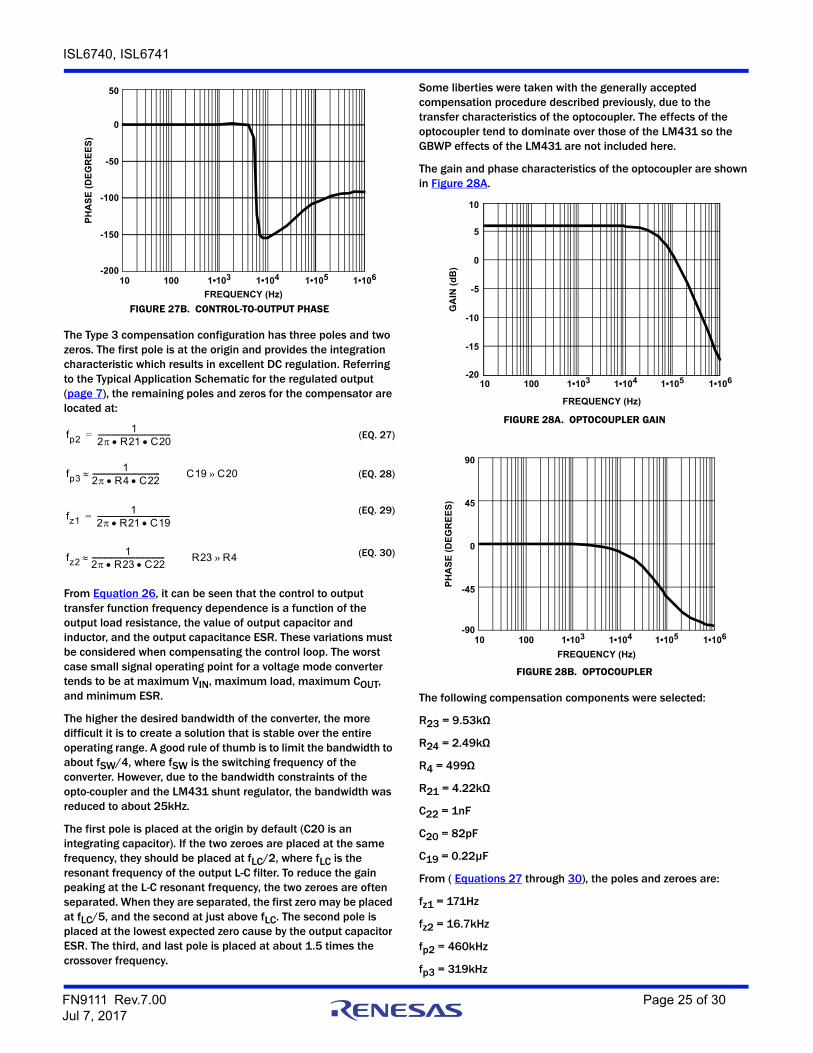
ISL6740, ISL6741
The Type 3 compensation configuration has three poles and two zeros. The first pole is at the origin and provides the integration characteristic which results in excellent DC regulation. Referring to the Typical Application Schematic for the regulated output (page 7), the remaining poles and zeros for the compensator are located at:
From Equation 26, it can be seen that the control to output transfer function frequency dependence is a function of the output load resistance, the value of output capacitor and inductor, and the output capacitance ESR. These variations must be considered when compensating the control loop. The worst case small signal operating point for a voltage mode converter tends to be at maximum VIN, maximum load, maximum COUT, and minimum ESR.
The higher the desired bandwidth of the converter, the more difficult it is to create a solution that is stable over the entire operating range. A good rule of thumb is to limit the bandwidth to about fSW/4, where fSW is the switching frequency of the converter. However, due to the bandwidth constraints of the opto-coupler and the LM431 shunt regulator, the bandwidth was reduced to about 25kHz.
The first pole is placed at the origin by default (C20 is an integrating capacitor). If the two zeroes are placed at the same frequency, they should be placed at fLC/2, where fLC is the resonant frequency of the output L-C filter. To reduce the gain peaking at the L-C resonant frequency, the two zeroes are often separated. When they are separated, the first zero may be placed at fLC/5, and the second at just above fLC. The second pole is placed at the lowest expected zero cause by the output capacitor ESR. The third, and last pole is placed at about 1.5 times the crossover frequency.
Some liberties were taken with the generally accepted compensation procedure described previously, due to the transfer characteristics of the optocoupler. The effects of the optocoupler tend to dominate over those of the LM431 so the GBWP effects of the LM431 are not included here.
The gain and phase characteristics of the optocoupler are shown in Figure 28A.
The following compensation components were selected:
R23 = 9.53kΩ
R24 = 2.49kΩ
R4 = 499Ω
R21 = 4.22kΩ
C22 = 1nF
C20 = 82pF
C19 = 0.22µF
From ( Equations 27 through 30), the poles and zeroes are:
fz1 = 171Hz
fz2 = 16.7kHz
fp2 = 460kHz
fp3 = 319kHz
FIGURE 27B. CONTROL-TO-OUTPUT PHASE
10 100 1•106-200
-150
-100
-50
0
50
FREQUENCY (Hz)
PH
AS
E (
DE
GR
EE
S)
1•1051•1041•103
fp21
2 R21 C20-----------------------------------------= (EQ. 27)
fp31
2 R4 C22-------------------------------------- C19 C20» (EQ. 28)
fz11
2 R21 C19-----------------------------------------=
(EQ. 29)
fz21
2 R23 C22----------------------------------------- R23 R4» (EQ. 30)
FIGURE 28A. OPTOCOUPLER GAIN
-20
-15
-10
-5
0
5
10
FREQUENCY (Hz)
GA
IN (
dB
)
10 100 1•1061•1051•1041•103
FIGURE 28B. OPTOCOUPLER
-90
-45
0
45
90
FREQUENCY (Hz)
PH
AS
E (
DE
GR
EE
S)
10 100 1•1061•1051•1041•103
FN9111 Rev.7.00 Page 25 of 30Jul 7, 2017
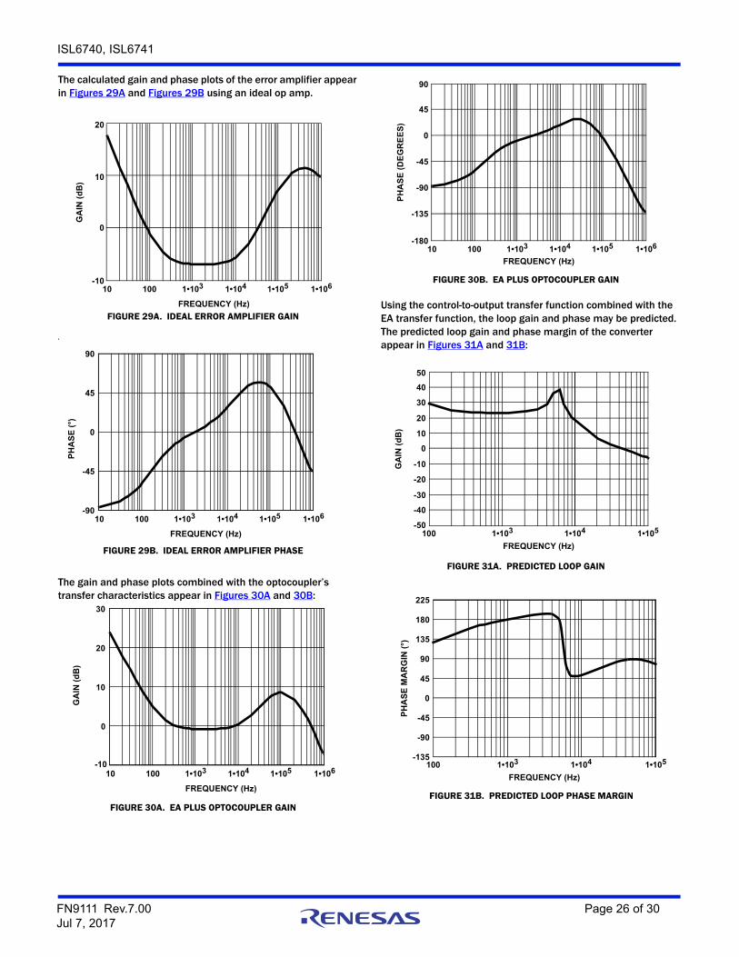
ISL6740, ISL6741
The calculated gain and phase plots of the error amplifier appear in Figures 29A and Figures 29B using an ideal op amp.
The gain and phase plots combined with the optocoupler’s transfer characteristics appear in Figures 30A and 30B:
Using the control-to-output transfer function combined with the EA transfer function, the loop gain and phase may be predicted. The predicted loop gain and phase margin of the converter appear in Figures 31A and 31B:
FIGURE 29A. IDEAL ERROR AMPLIFIER GAIN
-10
0
10
20
FREQUENCY (Hz)
GA
IN (
dB
)
10 100 1•1061•1051•1041•103
FIGURE 29B. IDEAL ERROR AMPLIFIER PHASE
-90
-45
0
45
90
FREQUENCY (Hz)
PH
AS
E (
°)
10 100 1•1061•1051•1041•103
FIGURE 30A. EA PLUS OPTOCOUPLER GAIN
-10
0
10
20
30
FREQUENCY (Hz)
GA
IN (
dB
)
10 100 1•1061•1051•1041•103
FIGURE 30B. EA PLUS OPTOCOUPLER GAIN
-180
-135
-90
-45
0
45
90
FREQUENCY (Hz)
PH
AS
E (
DE
GR
EE
S)
10 100 1•1061•1051•1041•103
FIGURE 31A. PREDICTED LOOP GAIN
-50
-40
-30
-20
-10
0
10
20
30
40
50
FREQUENCY (Hz)
GA
IN (
dB
)
100 1•1051•1041•103
FIGURE 31B. PREDICTED LOOP PHASE MARGIN
-135
-90
-45
0
45
90
135
180
225
FREQUENCY (Hz)
PH
AS
E M
AR
GIN
(°)
100 1•1051•1041•103
FN9111 Rev.7.00 Page 26 of 30Jul 7, 2017
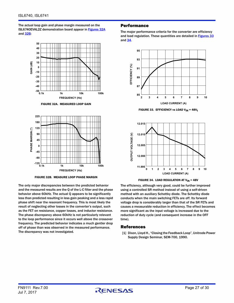
ISL6740, ISL6741
The actual loop gain and phase margin measured on the ISL6740EVAL2Z demonstration board appear in Figures 32A and 32B:
The only major discrepancies between the predicted behavior and the measured results are the Q of the L-C filter and the phase behavior above 60kHz. The actual Q appears to be significantly less than predicted resulting in less gain peaking and a less rapid phase shift near the resonant frequency. This is most likely the result of neglecting other losses in the converter’s output, such as the FET on resistance, copper losses, and inductor resistance. The phase discrepancy above 60kHz is not particularly relevant to the loop performance since it occurs well above the crossover frequency. The predicted behavior indicates a much gentler drop off of phase than was observed in the measured performance. The discrepancy was not investigated.
PerformanceThe major performance criteria for the converter are efficiency and load regulation. These quantities are detailed in Figures 33 and 34.
The efficiency, although very good, could be further improved using a controlled SR method instead of using a self-driven method with an auxiliary Schottky diode. The Schottky diode conducts when the main switching FETs are off. Its forward voltage drop is considerably larger than that of the SR FETs and causes a measurable reduction in efficiency. The effect becomes more significant as the input voltage is increased due to the reduction of duty cycle (and consequent increase in the OFF time).
References[1] Dixon, Lloyd H., “Closing the Feedback Loop”, Unitrode Power
Supply Design Seminar, SEM-700, 1990.
FIGURE 32A. MEASURED LOOP GAIN
0.1k 1k 10k 100k-50
-40
-30
-20
-10
0
10
20
30
40
50
FREQUENCY (Hz)
GA
IN (
dB
)
FIGURE 32B. MEASURE LOOP PHASE MARGIN
0.1k 1k 10k 100k-135
-90
-45
0
45
90
135
180
225
FREQUENCY (Hz)
PH
AS
E M
AR
GIN
(°)
FIGURE 33. EFFICIENCY vs LOAD VIN = 48Vt
2 3 4 5 6 7 8 9 1085
87
89
91
93
95
LOAD CURRENT (A)
EF
FIC
IEN
CY
(%
)
FIGURE 34. LOAD REGULATION AT VIN = 48V
0 1 2 3 4 5 6 7 8 9 1011.995
12.000
12.005
12.010
12.015
LOAD CURRENT (A)
OU
TP
UT
VO
LTA
GE
(V
)
FN9111 Rev.7.00 Page 27 of 30Jul 7, 2017
ISL6740, ISL6741
About IntersilIntersil Corporation is a leading provider of innovative power management and precision analog solutions. The company's products address some of the largest markets within the industrial and infrastructure, mobile computing, and high-end consumer markets.
For the most updated datasheet, application notes, related documentation, and related parts, see the respective product information page found at www.intersil.com.
For a listing of definitions and abbreviations of common terms used in our documents, visit www.intersil.com/glossary.
You can report errors or suggestions for improving this datasheet by visiting www.intersil.com/ask.
Reliability reports are also available from our website at www.intersil.com/support.
Revision History The revision history provided is for informational purposes only and is believed to be accurate, but not warranted. Please visit our website to make sure you have the latest revision.
DATE REVISION CHANGE
July 7, 2016 FN9111.7 • Added Table of Contents on page 2.• Typical Application diagram for ISL6740EVAL2Z on page 7: Corrected polarity of CR5 and CR6 and changed resistor R19 label (between VREF and VERROR) to R16.
• Moved Component List tables after their respective Typical Application diagrams.• Added Revision History and About Intersil sections.
FN9111 Rev.7.00 Page 28 of 30Jul 7, 2017
ISL6740, ISL6741
FN9111 Rev.7.00 Page 29 of 30Jul 7, 2017
Package Outline DrawingM16.17316 LEAD THIN SHRINK SMALL OUTLINE PACKAGE (TSSOP)
Rev 2, 5/10
0.09-0.20
SEE DETAIL "X"
DETAIL "X"
TYPICAL RECOMMENDED LAND PATTERN
TOP VIEW
SIDE VIEW
END VIEW
Dimension does not include mold flash, protrusions or gate burrs.
Mold flash, protrusions or gate burrs shall not exceed 0.15 per side.
Dimension does not include interlead flash or protrusion. Interlead
flash or protrusion shall not exceed 0.25 per side.
Dimensions are measured at datum plane H.
Dimensioning and tolerancing per ASME Y14.5M-1994.
Dimension does not include dambar protrusion. Allowable protrusion
shall be 0.08mm total in excess of dimension at maximum material
condition. Minimum space between protrusion and adjacent lead
is 0.07mm.
Dimension in ( ) are for reference only.
Conforms to JEDEC MO-153.
6.
3.
5.
4.
2.
1.
NOTES:
7.
(0.65 TYP)
(5.65)
(0.35 TYP)
0.90 +0.15/-0.10
0.60 ±0.150.15 MAX
0.05 MIN
PLANEGAUGE
0°-8°
0.25
1.00 REF
(1.45)
16
2
1
3
8
B
1 3
9
A
PIN #1I.D. MARK
5.00 ±0.10
6.40
4.40 ±0.10
0.65
1.20 MAX
SEATINGPLANE
0.25 +0.05/-0.06 5
C
H
0.20 C B A
0.10 C
- 0.05
0.10 C B AM
For the most recent package outline drawing, see M16.173.
FN9111 Rev.7.00 Page 30 of 30Jul 7, 2017
ISL6740, ISL6741
Intersil products are manufactured, assembled and tested utilizing ISO9001 quality systems as notedin the quality certifications found at www.intersil.com/en/support/qualandreliability.html
Intersil products are sold by description only. Intersil may modify the circuit design and/or specifications of products at any time without notice, provided that such modification does not, in Intersil's sole judgment, affect the form, fit or function of the product. Accordingly, the reader is cautioned to verify that datasheets are current before placing orders. Information furnished by Intersil is believed to be accurate and reliable. However, no responsibility is assumed by Intersil or its subsidiaries for its use; nor for any infringements of patents or other rights of third parties which may result from its use. No license is granted by implication or otherwise under any patent or patent rights of Intersil or its subsidiaries.
For information regarding Intersil Corporation and its products, see www.intersil.com
For additional products, see www.intersil.com/en/products.html
© Copyright Intersil Americas LLC 2003-2017. All Rights Reserved.All trademarks and registered trademarks are the property of their respective owners.
Small Outline Plastic Packages (SOIC)
NOTES:
1. Symbols are defined in the “MO Series Symbol List” in Section 2.2 of Publication Number 95.
2. Dimensioning and tolerancing per ANSI Y14.5M-1982.
3. Dimension “D” does not include mold flash, protrusions or gate burrs. Mold flash, protrusion and gate burrs shall not exceed 0.15mm (0.006 inch) per side.
4. Dimension “E” does not include interlead flash or protrusions. Interlead flash and protrusions shall not exceed 0.25mm (0.010 inch) per side.
5. The chamfer on the body is optional. If it is not present, a visual index feature must be located within the crosshatched area.
6. “L” is the length of terminal for soldering to a substrate.
7. “N” is the number of terminal positions.
8. Terminal numbers are shown for reference only.
9. The lead width “B”, as measured 0.36mm (0.014 inch) or greater above the seating plane, shall not exceed a maximum value of 0.61mm (0.024 inch).
10. Controlling dimension: MILLIMETER. Converted inch dimensions are not necessarily exact.
INDEXAREA
E
D
N
1 2 3
-B-
0.25(0.010) C AM B S
e
-A-
L
B
M
-C-
A1
A
SEATING PLANE
0.10(0.004)
h x 45°
C
H 0.25(0.010) BM M
M16.15 (JEDEC MS-012-AC ISSUE C)
16 LEAD NARROW BODY SMALL OUTLINE PLASTIC PACKAGE
SYMBOL
INCHES MILLIMETERS
NOTESMIN MAX MIN MAX
A 0.0532 0.0688 1.35 1.75 -
A1 0.0040 0.0098 0.10 0.25 -
B 0.013 0.020 0.33 0.51 9
C 0.0075 0.0098 0.19 0.25 -
D 0.3859 0.3937 9.80 10.00 3
E 0.1497 0.1574 3.80 4.00 4
e 0.050 BSC 1.27 BSC -
H 0.2284 0.2440 5.80 6.20 -
h 0.0099 0.0196 0.25 0.50 5
L 0.016 0.050 0.40 1.27 6
N 16 16 7
0° 8° 0° 8° -
Rev. 1 6/05
For the most recent package outline drawing, see M16.15.