Embed Size (px)
Citation preview
REI Datasheet
© 2013 Rochester Electronics, LLC. All Rights Reserved 10232013
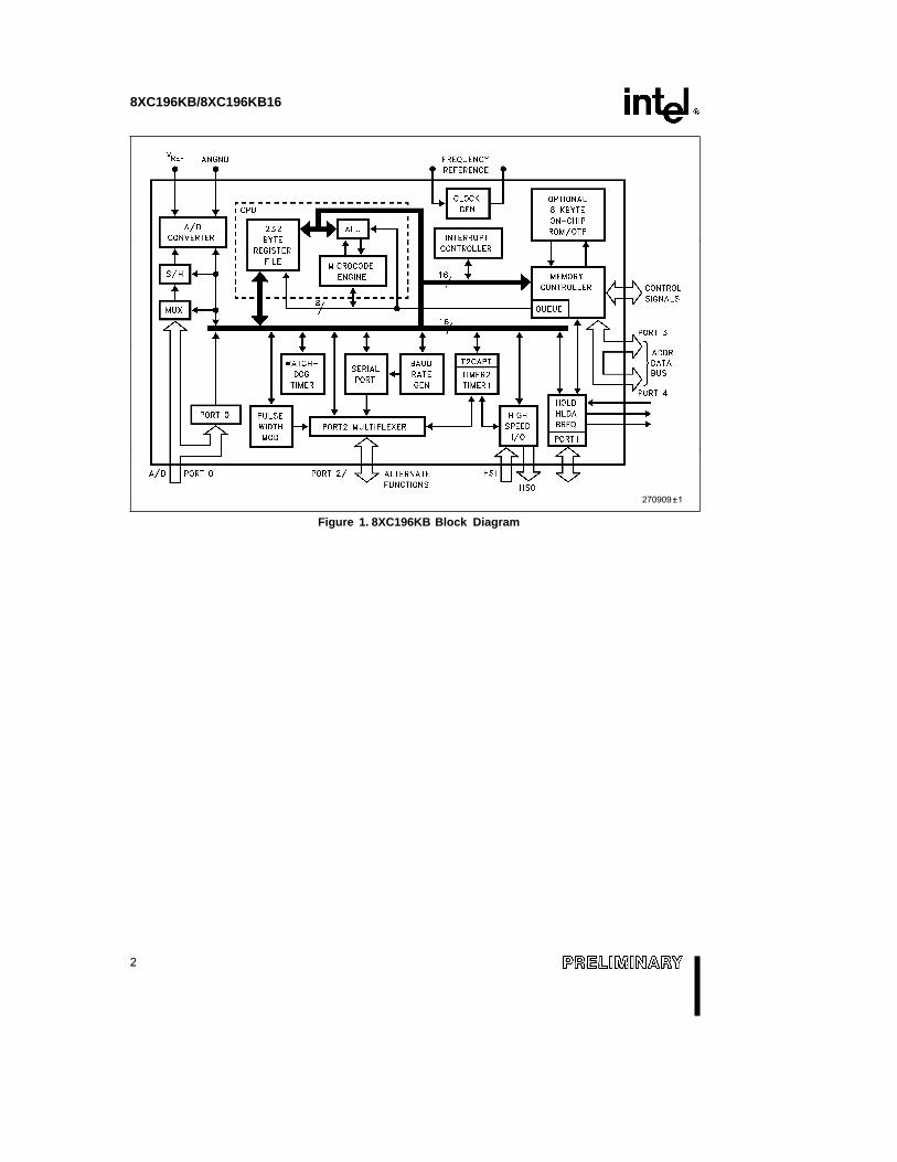
The 8XC196KB is a 16-bit microcontroller is a high performance member of the MCS 96 microcontroller family. The 8XC196KB has the same peripheral set as the 8096BH and has a true superset of the 8096BH instructions. Intel’s CHMOS process provides a high performance processor along with low power consumption. To further reduce power requirements, the processor can be placed into Idle or Powerdown Mode.
Four high-speed capture inputs are provided to record times when events occur. Six high-speed outputs are available for pulse or waveform generation. The high-speed output can also generate four software timers or start an A/D conversion. Events can be based on the timer or up/down counter. Also provided on-chip are an A/D converter, serial port, watchdog timer, and a pulse-width-modulated output signal.
80C196KB, 87C196KBCommercial/Express CHMOS Microcontroller
The original manufacturer’s datasheet accompanying this document reflects the performance and specifications of the Rochester manufactured version of this device. Rochester Electronics guarantees the performance of its semiconductor products to the original OEM specifications. ‘Typical’ values are for reference purposes only. Certain minimum or maximum ratings may be based on product characterization, design, simulation, or sample testing.
To learn more, please visit www.rocelec.com
Quality Overview
••• • •• •
ISO-9001AS9120certificationQualifiedManufacturersList(QML)MIL-PRF-38535 Class Q MilitaryClassVSpaceLevelQualifiedSuppliersListofDistributors(QSLD)RochesterisacriticalsuppliertoDLAandmeetsallindustryandDLAstandards.
RochesterElectronics,LLCiscommittedtosupplyingproducts that satisfy customer expectations for quality and are equal to those originally supplied by industry manufacturers.
Rochester Electronics Manufactured Components
Rochester branded components aremanufactured using either die/wafers purchased from the original suppliers orRochesterwafersrecreatedfromtheoriginal IP. All recreations are done with the approval of the OCM.
Parts are tested using original factory testprogramsorRochesterdevelopedtest solutions to guarantee product meets or exceeds the OCM data sheet.
*Other brands and names are the property of their respective owners.Information in this document is provided in connection with Intel products. Intel assumes no liability whatsoever, including infringement of any patent orcopyright, for sale and use of Intel products except as provided in Intel's Terms and Conditions of Sale for such products. Intel retains the right to makechanges to these specifications at any time, without notice. Microcomputer Products may have minor variations to this specification known as errata.
July 2004COPYRIGHT © INTEL CORPORATION,2004 Order Number: 270909-007
8XC196KB/8XC196KB16COMMERCIAL/EXPRESS CHMOS MICROCONTROLLER
Y 8 Kbytes of On-Chip ROM/OTPAvailable
Y 232 Byte Register FileY Register-to-Register ArchitectureY 28 Interrupt Sources/16 VectorsY 1.75 ms 16 x 16 Multiply (16 MHz)Y 3.0 ms 32/16 Divide (16 MHz)Y Powerdown and Idle ModesY Five 8-Bit I/O PortsY 16-Bit Watchdog TimerY 12 MHz and 16 MHz AvailableY Dedicated 15-Bit Baud Rate Generator
Y Dynamically Configurable 8-Bit or16-Bit Buswidth
Y Full Duplex Serial PortY High Speed I/O SubsystemY 16-Bit TimerY 16-Bit Up/Down Counter with CaptureY Pulse-Width-Modulated OutputY Four 16-Bit Software TimersY 10-Bit A/D Converter with Sample/HoldY HOLD/HLDA Bus ProtocolY Extended Temperature Available
The 8XC196KB is a 16-bit microcontroller available in three different memory varieties: ROMless (80C196KB),8K ROM (83C196KB) and 8K OTP (One Time Programmable-87C196KB). The 8XC196KB is a high perform-ance member of the MCSÉ 96 microcontroller family. The 8XC196KB has the same peripheral set as the8096BH and has a true superset of the 8096BH instructions. Intel's CHMOS process provides a high perform-ance processor along with low power consumption. To further reduce power requirements, the processor canbe placed into Idle or Powerdown Mode.
Bit, byte, word and some 32-bit operations are available on the 80C196KB. With a 16 MHz oscillator a 16-bitaddition takes 0.50 ms, and the instruction times average 0.37 ms to 1.1 ms in typical applications.
Four high-speed capture inputs are provided to record times when events occur. Six high-speed outputs areavailable for pulse or waveform generation. The high-speed output can also generate four software timers orstart an A/D conversion. Events can be based on the timer or up/down counter. Also provided on-chip are anA/D converter, serial port, watchdog timer and a pulse-width-modulated output signal.
The 8XC196KB has a maximum guaranteed frequency of 12 MHz. The 8XC196KB16 has a maximum guaran-teed frequency of 16 MHz. All references to the 80C196KB also refer to the 80C196KB16; 83C196KB, Rxxx;87C196KB and 87C196KB16 unless otherwise noted. The ROM device does not have a speed indicator at theend of the device name. Instead it has a ROM code number.
With the commercial (standard) temperature option, operational characteristics are guaranteed over the tem-perature range of 0§C to a70§C. With the extended temperature range option, operational characteristics areguaranteed over the temperature range of b40§C to a85§C.
*Other brands and names are the property of their respective owners.
8XC196KB/8XC196KB16
270909±1
Figure 1. 8XC196KB Block Diagram
2
8XC196KB/8XC196KB16
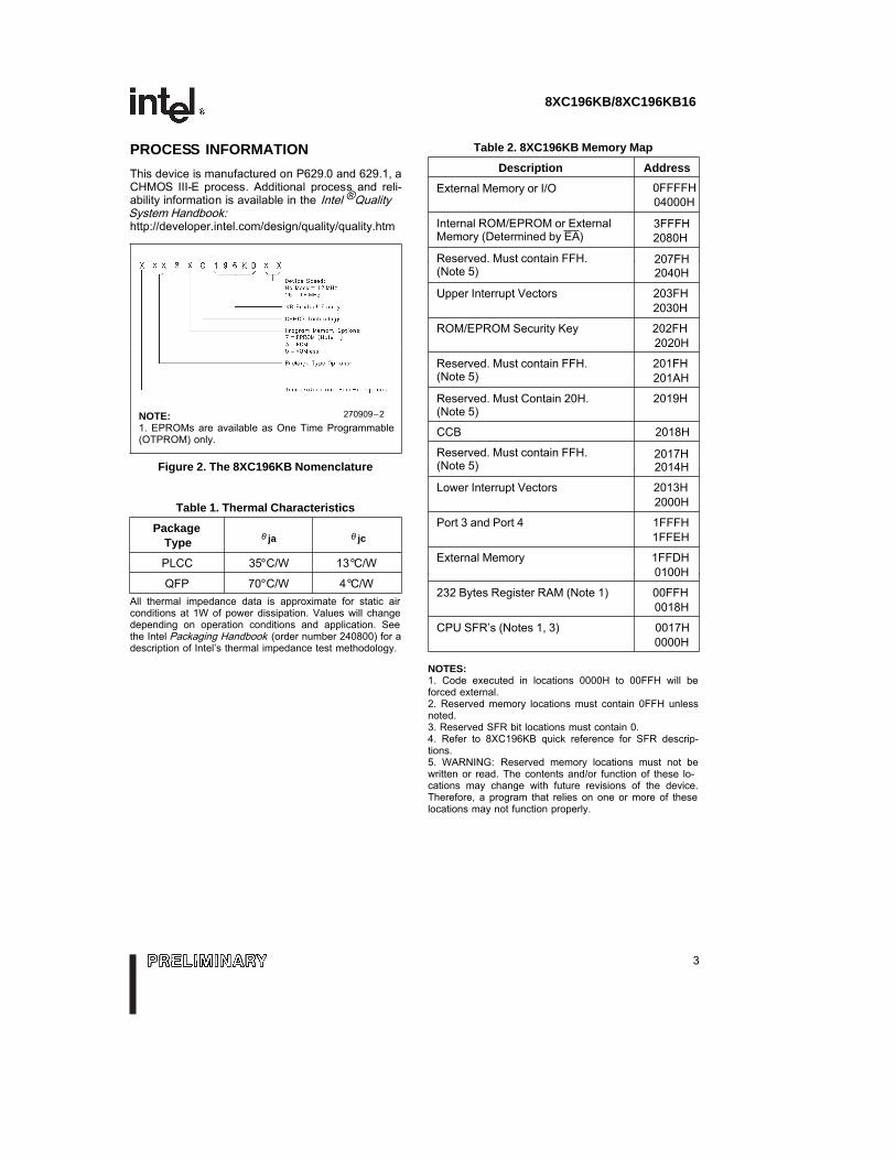
PROCESS INFORMATIONThis device is manufactured on P629. 0 and 629.1, aCHMOS III-E process. Additional process and reli-ability information is available in the Intel ® QualitySystem Handbook:http://developer.intel.com/design/quality/quality.htm
270909–2NOTE:1. EPROMs are available as One Time Programmable(OTPROM) only.
Figure 2. The 8XC196KB Nomenclature
Table 1. Thermal Characteristics
Packageθ ja θ jcType
PLCC 35°C/W 13°C/W
QFP 70°C/W 4°C/WAll thermal impedance data is approximate for static airconditions at 1W of power dissipation. Values will changedepending on operation conditions and application. Seethe Intel Packaging Handbook (order number 240800) for adescription of Intel’s thermal impedance test methodology.
Table 2. 8XC196KB Memory Map
Description Address
External Memory or I/O04000H
Internal ROM/EPROM or ExternalMemory (Determined by EA) 2080H
Reserved. Must contain FFH.(Note 5) 2040H
Upper Interrupt Vectors 203FH2030H
ROM/EPROM Security Key 202FH2020H
Reserved. Must contain FFH.(Note 5) 201AH
Reserved. Must Contain 20H.(Note 5)
CCB 2018H
Reserved. Must contain FFH.(Note 5) 2014H
Lower Interrupt Vectors 2013H2000H
Port 3 and Port 4 1FFFH1FFEH
External Memory 1FFDH0100H
232 Bytes Register RAM (Note 1) 00FFH0018H
CPU SFR’s (Notes 1, 3) 0017H0000H
NOTES:1. Code executed in locations 0000H to 00FFH will beforced external.2. Reserved memory locations must contain 0FFH unlessnoted.3. Reserved SFR bit locations must contain 0.4. Refer to 8XC196KB quick reference for SFR descrip-tions.5. WARNING: Reserved memory locations must not bewritten or read. The contents and/or function of these lo-cations may change with future revisions of the device.Therefore, a program that relies on one or more of theselocations may not function properly.
3
207FH
201FH
2019H
2017H
0FFFFH
3FFFH
8XC196KB/8XC196KB16
270909–3
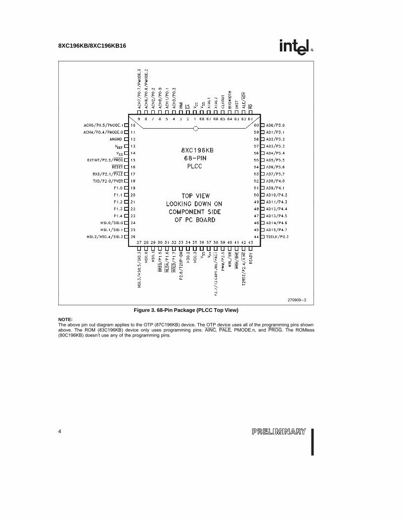
Figure 3. 68-Pin Package (PLCC Top View)
NOTE:The above pin out diagram applies to the OTP (87C196KB) device. The OTP device uses all of the programming pins shownabove. The ROM (83C196KB) device only uses programming pins: AINC, PALE, PMODE.n, and PROG. The ROMless(80C196KB) doesn’t use any of the programming pins.
4
8XC196KB/8XC196KB16
270909–4
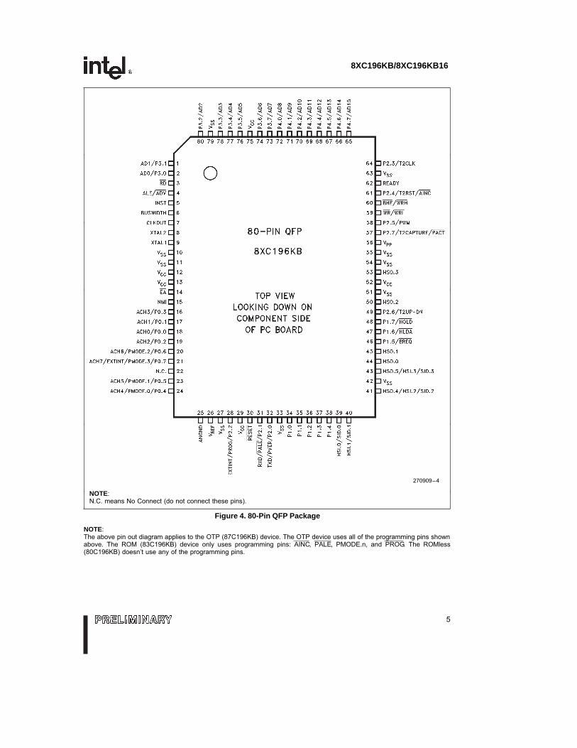
NOTE:N.C. means No Connect (do not connect these pins).
Figure 4. 80-Pin QFP Package
NOTE:The above pin out diagram applies to the OTP (87C196KB) device. The OTP device uses all of the programming pins shownabove. The ROM (83C196KB) device only uses programming pins: AINC, PALE, PMODE.n, and PROG. The ROMless(80C196KB) doesn’t use any of the programming pins.
5
8XC196KB/8XC196KB16
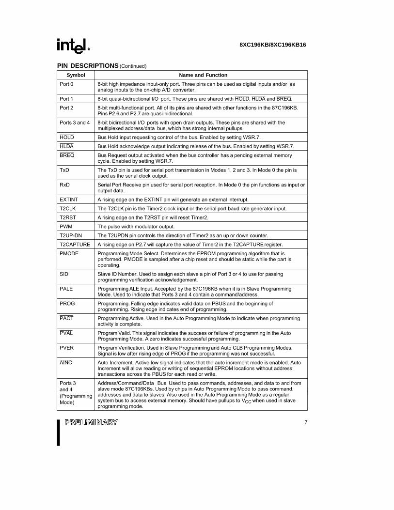
PIN DESCRIPTIONSSymbol Name and Function
VCC Main supply voltage (5V).
VSS Digital circuit ground (0V). There are multiple VSS pins, all of them must be connected.
VREF Reference voltage for the A/D converter (5V). VREF is also the supply voltage to the analogportion of the A/D converter and the logic used to read Port 0. Must be connected for A/Dand Port 0 to function.
ANGND Reference ground for the A/D converter. Must be held at nominally the same potential asVSS. Connect VSS and ANGND at chip to avoid noise problems.
VPP Programming voltage. Also timing pin for the return from power down circuit.
XTAL1 Input of the oscillator inverter and of the internal clock generator.
XTAL2 Output of the oscillator inverter.
CLKOUT Output of the internal clock generator. The frequency of CLKOUT is (/2 the oscillatorfrequency. It has a 50% duty cycle.
RESET Reset input to and open-drain output from the chip. Input low for at least 4 state times to resetthe chip. The subsequent low-to-high transition re-synchronizes CLKOUT and commences a10-state-time RESET sequence.
BUSWIDTH Input for buswidth selection. If CCR bit 1 is a one, this pin selects the bus width for the buscycle in progress. If BUSWIDTH is a 1, a 16-bit bus cycle occurs. If BUSWIDTH is a 0 an 8-bitcycle occurs. If CCR bit 1 is a 0, the bus is always an 8-bit bus.
NMI A positive transition causes a vector through 203EH.
INST Output high during an external memory read indicates the read is an instruction fetch andoutput low indicates a data fetch. INST is valid throughout the bus cycle. INST is activatedonly during external memory accesses.
EA Input for memory select (External Access). EA equal to a TTL-high causes memory accessesto locations 2000H through 3FFFH to be directed to on-chip ROM/OTPR OM. EA equal to aTTL-low causes accesses to these locations to be directed to off-chip memory.
ALE/ADV Address Latch Enable or Address Valid output, as selected by CCR. Both pin options providea latch to demultiplex the address from the address/data bus. When the pin is ADV, it goesinactive high at the end of the bus cycle. ALE/ADV is activated only during external memoryaccesses.
RD Read signal output to external memory. RD is activated only during external memory reads.
WR/WRL Write and Write Low output to external memory, as selected by the CCR. WR will go low forevery external write, while WRL will go low only for external writes where an even byte isbeing written. WR/WRL is activated only during external memory writes.
BHE/WRH Bus High Enable or Write High output to external memory, as selected by the CCR. BHE willgo low for external writes to the high byte of the data bus. WRH will go low for external writeswhere an odd byte is being addressed. BHE/WRH is activated only during external memorywrites.
READY Ready input to lengthen external memory cycles. If the pin is low prior to the falling edge ofCLKOUT, the memory controller goes into a wait mode until the next positive transition inCLKOUT occurs with READY high. When the external memory is not being used, READY hasno effect. Internal control of the number of wait states inserted into a bus cycle (held notready) is available in the CCR.
HSI Inputs to High Speed Input Unit. Four HSI pins are available: HSI.0, HSI.1, HSI.2 and HSI.3.Two of them (HSI.2 and HSI.3) are shared with the HSO Unit.
HSO Outputs from High Speed Output Unit. Six HSO pins are available: HSO.0, HSO.1, HSO.2,HSO.3, HSO.4 and HSO.5. Two of them (HSO.4 and HSO.5) are shared with the HSI Unit.
6
8XC196KB/8XC196KB16
PIN DESCRIPTIONS (Continued)
Symbol Name and Function
Port 0 8-bit high impedance input-only port. Three pins can be used as digital inputs and/or asanalog inputs to the on-chip A/D converter.
Port 1 8-bit quasi-bidirectional I/O port. These pins are shared with HOLD, HLDA and BREQ.
Port 2 8-bit multi-functional port. All of its pins are shared with other functions in the 87C196KB.Pins P2.6 and P2.7 are quasi-bidirectional.
Ports 3 and 4 8-bit bidirectional I/O ports with open drain outputs. These pins are shared with themultiplexed address/data bus, which has strong internal pullups.
HOLD Bus Hold input requesting control of the bus. Enabled by setting WSR.7.
HLDA Bus Hold acknowledge output indicating release of the bus. Enabled by setting WSR.7.
BREQ Bus Request output activated when the bus controller has a pending external memorycycle. Enabled by setting WSR.7.
TxD The TxD pin is used for serial port transmission in Modes 1, 2 and 3. In Mode 0 the pin isused as the serial clock output.
RxD Serial Port Receive pin used for serial port reception. In Mode 0 the pin functions as input oroutput data.
EXTINT A rising edge on the EXTINT pin will generate an external interrupt.
T2CLK The T2CLK pin is the Timer2 clock input or the serial port baud rate generator input.
T2RST A rising edge on the T2RST pin will reset Timer2.
PWM The pulse width modulator output.
T2UP-DN The T2UPDN pin controls the direction of Timer2 as an up or down counter.
T2CAPTURE A rising edge on P2.7 will capture the value of Timer2 in the T2CAPTURE register.
PMODE Programming Mode Select. Determines the EPROM programming algorithm that isperformed. PMODE is sampled after a chip reset and should be static while the part isoperating.
SID Slave ID Number. Used to assign each slave a pin of Port 3 or 4 to use for passingprogramming verification acknowledgement.
PALE Programming ALE Input. Accepted by the 87C196KB when it is in Slave ProgrammingMode. Used to indicate that Ports 3 and 4 contain a command/address.
PROG Programming. Falling edge indicates valid data on PBUS and the beginning ofprogramming. Rising edge indicates end of programming.
PACT Programming Active. Used in the Auto Programming Mode to indicate when programmingactivity is complete.
PVAL Program Valid. This signal indicates the success or failure of programming in the AutoProgramming Mode. A zero indicates successful programming.
PVER Program Verification. Used in Slave Programming and Auto CLB Programming Modes.Signal is low after rising edge of PROG if the programming was not successful.
AINC Auto Increment. Active low signal indicates that the auto increment mode is enabled. AutoIncrement will allow reading or writing of sequential EPROM locations without addresstransactions across the PBUS for each read or write.
Ports 3 Address/Command/Data Bus. Used to pass commands, addresses, and data to and fromslave mode 87C196KBs. Used by chips in Auto Programming Mode to pass command,and 4addresses and data to slaves. Also used in the Auto Programming Mode as a regular(Programmingsystem bus to access external memory. Should have pullups to VCC when used in slaveMode)programming mode.
7
8XC196KB/8XC196KB16
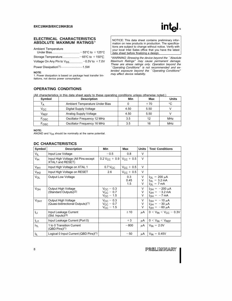
ELECTRICAL CHARACTERISTICSABSOLUTE MAXIMUM RATINGS*
Ambient TemperatureUnder Bias.................................b55§C to a125§C
Storage Temperature....................b65§C to a150§CVoltage On Any Pin to VSS................b0.5V to a7.0V
Power Dissipation(1)..........................1.5W
NOTE:1. Power dissipation is based on package heat transfer lim-itations, not device power consumption.
NOTICE: This data sheet contains preliminary infor-mation on new products in production. The specifica-tions are subject to change without notice. Verify withyour local Intel Sales office that you have the latestdata sheet before finalizing a design.
*WARNING: Stressing the device beyond the ``AbsoluteMaximum Ratings'' may cause permanent damage.These are stress ratings only. Operation beyond the``Operating Conditions'' is not recommended and ex-tended exposure beyond the ``Operating Conditions''may affect device reliability.
OPERATING CONDITIONS(All characteristics in this data sheet apply to these operating conditions unless otherwise noted.)
Symbol Description Min Max UnitsTA Ambient Temperature Under Bias 0 a70 §CVCC Digital Supply Voltage 4.50 5.50 VVREF Analog Supply Voltage 4.50 5.50 VFOSC Oscillator Frequency 12 MHz 3.5 12 MHzFOSC Oscillator Frequency 16 MHz 3.5 16 MHz
NOTE:ANGND and VSS should be nominally at the same potential.
DC CHARACTERISTICSSymbol Description Min Max Units Test ConditionsVIL Input Low Voltage b0.5 0.8 VVIH Input High Voltage (All Pins except 0.2 VCC a 0.9 VCC a 0.5 V
XTAL1 and RESET)VIH1 Input High Voltage on XTAL 1 0.7 VCC VCC a 0.5 VVIH2 Input High Voltage on RESET 2.6 VCC a 0.5 VVOL Output Low Voltage 0.3 V IOL e 200 mA
0.45 V IOL e 3.2 mA1.5 V IOL e 7 mA
VOH Output High Voltage VCC b 0.3 V IOH e b200 mA(Standard Outputs)(2) VCC b 0.7 V IOH e b3.2 mA
VCC b 1.5 V IOH e b7 mAVOH1 Output High Voltage VCC b 0.3 V IOH e b10 mA
(Quasi-bidirectional Outputs)(1) VCC b 0.7 V IOH e b30 mAVCC b 1.5 V IOH e b60 mA
ILI Input Leakage Current g10 mA 0 k VIN k VCC b 0.3V(Std. Inputs)(3)
ILI1 Input Leakage Current (Port 0) a3 mA 0 k VIN k VREFITL 1 to 0 Transition Current b800 mA VIN e 2.0V
(QBD Pins)(1)
IIL Logical 0 Input Current (QBD Pins)(1) b50 mA VIN e 0.45V
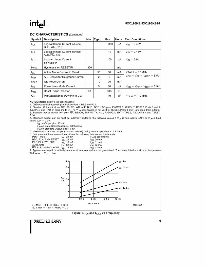
8
8XC196KB/8XC196KB16
DC CHARACTERISTICS (Continued)
Symbol Description Min Typ(7) Max Units Test Conditions
IIL1 Logical 0 Input Current in Reset b850 mA VIN e 0.45VBHE, WR, P2.0
IIL2 Logical 0 Input Current in Reset b7 mA VIN e 0.45VALE, RD, INST
IIH1 Logical 1 Input Current 100 mA VIN e 2.0Von NMI Pin
Hyst. Hysteresis on RESET Pin 300 mV
ICC Active Mode Current in Reset 50 60 mA XTAL1 e 16 MHz
IREF A/D Converter Reference Current 2 5 mA VCC e VPP e VREF e 5.5V
IIDLE Idle Mode Current 10 25 mA
IPD Powerdown Mode Current 5 30 mA VCC e VPP e VREF e 5.5V
RRST Reset Pullup Resistor 6K 50K X
CS Pin Capacitance (Any Pin to VSS) 10 pF FTEST e 1.0 MHz
NOTES: (Notes apply to all specifications)1. QBD (Quasi-bidirectional) pins include Port 1, P2.6 and P2.7.2. Standard Outputs include AD0±15, RD, WR, ALE, BHE, INST, HSO pins, PWM/P2.5, CLKOUT, RESET, Ports 3 and 4,TXD/P2.0 and RXD (in serial mode 0). The VOH specification is not valid for RESET. Ports 3 and 4 are open-drain outputs.3. Standard Inputs include HSI pins, EA, READY, BUSWIDTH, NMI, RXD/P2.1, EXTINT/P2.2, T2CLK/P2.3 and T2RST/P2.4.4. Maximum current per pin must be externally limited to the following values if VOL is held above 0.45V or VOH is heldbelow VCC b 0.7V:
IOL on Output pins: 10 mAIOH on quasi-bidirectional pins: self limitingIOH on Standard Output pins: 10 mA
5. Maximum current per bus pin (data and control) during normal operation is g3.2 mA.6. During normal (non-transient) conditions the following total current limits apply:
Port 1, P2.6 IOL: 29 mA IOH is self limitingHSO, P2.0, RXD, RESET IOL: 29 mA IOH: 26 mAP2.5, P2.7, WR, BHE IOL: 13 mA IOH: 11 mAAD0±AD15 IOL: 52 mA IOH: 52 mARD, ALE, INST±CLKOUT IOL: 13 mA IOH: 13 mA
7. Typicals are based on a limited number of samples and are not guaranteed. The values listed are at room temperatureand VREF e VCC e 5V.
ICC Max e 3.88 c FREQ a 8.43 270909±5IIDLE Max e 1.65 c FREQ a 2.2
Figure 6. ICC and IIDLE vs Frequency
9
8XC196KB/8XC196KB16
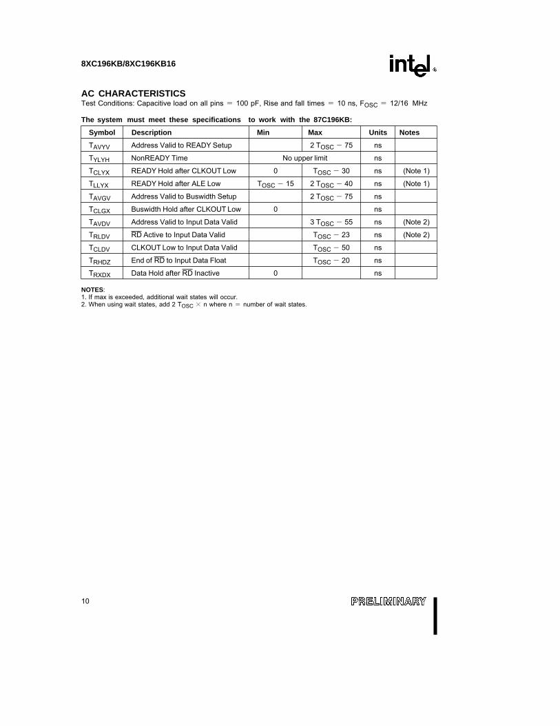
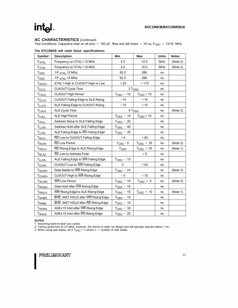
AC CHARACTERISTICSTest Conditions: Capacitive load on all pins e 100 pF, Rise and fall times e 10 ns, FOSC e 12/16 MHz
The system must meet these specifications to work with the 87C196KB:
Symbol Description Min Max Units Notes
TAVYV Address Valid to READY Setup 2 TOSC b 75 ns
TYLYH NonREADY Time No upper limit ns
TCLYX READY Hold after CLKOUT Low 0 TOSC b 30 ns (Note 1)
TLLYX READY Hold after ALE Low TOSC b 15 2 TOSC b 40 ns (Note 1)
TAVGV Address Valid to Buswidth Setup 2 TOSC b 75 ns
TCLGX Buswidth Hold after CLKOUT Low 0 ns
TAVDV Address Valid to Input Data Valid 3 TOSC b 55 ns (Note 2)
TRLDV RD Active to Input Data Valid TOSC b 23 ns (Note 2)
TCLDV CLKOUT Low to Input Data Valid TOSC b 50 ns
TRHDZ End of RD to Input Data Float TOSC b 20 ns
TRXDX Data Hold after RD Inactive 0 ns
NOTES:1. If max is exceeded, additional wait states will occur.2. When using wait states, add 2 TOSC c n where n e number of wait states.
10
8XC196KB/8XC196KB16
AC CHARACTERISTICS (Continued)Test Conditions: Capacitive load on all pins e 100 pF, Rise and fall times e 10 ns, FOSC e 12/16 MHz
The 87C196KB will meet these specifications:
Symbol Description Min Max Units Notes
FXTAL Frequency on XTAL1 12 MHz 3.5 12.0 MHz (Note 2)
FXTAL Frequency on XTAL1 16 MHz 3.5 16.0 MHz (Note 2)
TOSC 1/F XTAL 12 MHz 83.3 286 ns
TOSC 1/F XTAL 16 MHz 62.5 286 ns
TXHCH XTAL1 High to CLKOUT High or Low a20 a110 ns
TCLCL CLKOUT Cycle Time 2 TOSC ns
TCHCL CLKOUT High Period TOSC b 10 TOSCa10 ns
TCLLH CLKOUT Falling Edge to ALE Rising b10 a10 ns
TLLCH ALE Falling Edge to CLKOUT Rising b15 a15 ns
TLHLH ALE Cycle Time 4 TOSC ns (Note 3)
TLHLL ALE High Period TOSC b 10 TOSCa10 ns
TAVLL Address Setup to ALE Falling Edge TOSC b 20 ns
TLLAX Address Hold after ALE Falling Edge TOSC b 40 ns
TLLRL ALE Falling Edge to RD Falling Edge TOSC b 35 ns
TRLCL RD Low to CLKOUT Falling Edge a4 a25 ns
TRLRH RD Low Period TOSCb5 TOSC a 25 ns (Note 3)
TRHLH RD Rising Edge to ALE Rising Edge TOSC TOSC a 25 ns (Note 1)
TRLAZ RD Low to Address Float a5 ns
TLLWL ALE Falling Edge to WR Falling Edge TOSC b 10 ns
TCLWL CLKOUT Low to WR Falling Edge 0 a25 ns
TQVWH Data Stable to WR Rising Edge TOSC b 23 ns (Note 3)
TCHWH CLKOUT High to WR Rising Edge b5 a15 ns
TWLWH WR Low Period TOSC b 15 TOSC a 5 ns (Note 3)
TWHQX Data Hold after WR Rising Edge TOSC b 15 ns
TWHLH WR Rising Edge to ALE Rising Edge TOSC b 15 TOSC a 10 ns (Note 1)
TWHBX BHE, INST HOLD after WR Rising Edge TOSC b 15 ns
TRHBX BHE, INST HOLD after RD Rising Edge TOSC b 10 ns
TWHAX AD8±15 hold after WR Rising Edge TOSC b 30 ns
TRHAX AD8±15 hold after RD Rising Edge TOSC b 25 ns
NOTES:1. Assuming back-to-back bus cycles.2. Testing performed at 3.5 MHz, however, the device is static by design and will typically operate below 1 Hz.3. When using wait states, all 2 TOSCa n where n e number of wait states.
11
8XC196KB/8XC196KB16
System Bus Timings
270909±6
12
8XC196KB/8XC196KB16
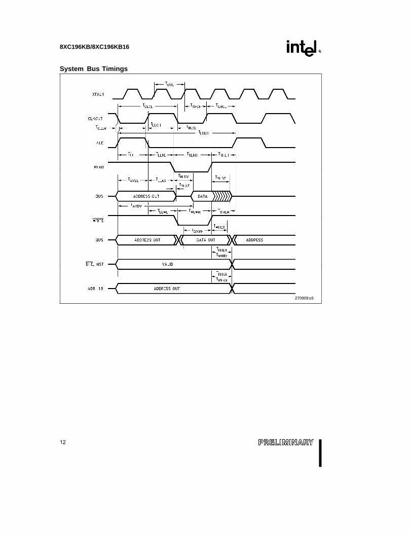
READY Timings (One Wait State)
270909±7
Buswidth Bus Timings
270909±8
13
8XC196KB/8XC196KB16
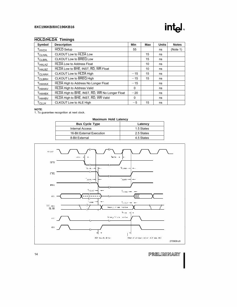
HOLD/HLDA TimingsSymbol Description Min Max Units NotesTHVCH HOLD Setup 55 ns (Note 1)TCLHAL CLKOUT Low to HLDA Low 15 nsTCLBRL CLKOUT Low to BREQ Low 15 nsTHALAZ HLDA Low to Address Float 10 nsTHALBZ HLDA Low to BHE, INST, RD, WR Float 10 nsTCLHAH CLKOUT Low to HLDA High b15 15 nsTCLBRH CLKOUT Low to BREQ High b15 15 nsTHAHAX HLDA High to Address No Longer Float b15 nsTHAHAV HLDA High to Address Valid 0 nsTHAHBX HLDA High to BHE, INST, RD, WR No Longer Float b20 nsTHAHBV HLDA High to BHE, INST, RD, WR Valid 0 nsTCLLH CLKOUT Low to ALE High b5 15 ns
NOTE:1. To guarantee recognition at next clock.
Maximum Hold LatencyBus Cycle Type Latency
Internal Access 1.5 States16-Bit External Execution 2.5 States8-Bit External 4.5 States
270909±9
14
8XC196KB/8XC196KB16
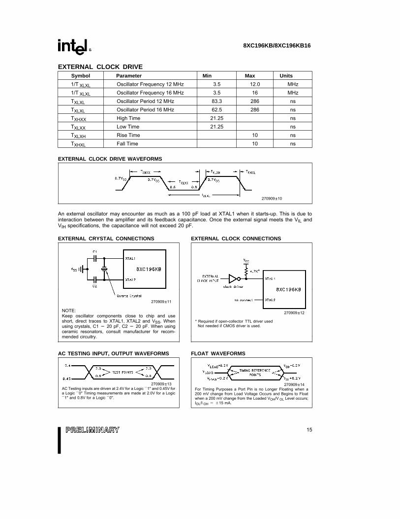
EXTERNAL CLOCK DRIVESymbol Parameter Min Max Units1/T XLXL Oscillator Frequency 12 MHz 3.5 12.0 MHz1/T XLXL Oscillator Frequency 16 MHz 3.5 16 MHzTXLXL Oscillator Period 12 MHz 83.3 286 nsTXLXL Oscillator Period 16 MHz 62.5 286 nsTXHXX High Time 21.25 nsTXLXX Low Time 21.25 nsTXLXH Rise Time 10 nsTXHXL Fall Time 10 ns
EXTERNAL CLOCK DRIVE WAVEFORMS
270909±10
An external oscillator may encounter as much as a 100 pF load at XTAL1 when it starts-up. This is due tointeraction between the amplifier and its feedback capacitance. Once the external signal meets the VIL andVIH specifications, the capacitance will not exceed 20 pF.
EXTERNAL CRYSTAL CONNECTIONS
270909±11
NOTE:Keep oscillator components close to chip and useshort, direct traces to XTAL1, XTAL2 and VSS. Whenusing crystals, C1 e 20 pF, C2 e 20 pF. When usingceramic resonators, consult manufacturer for recom-mended circuitry.
EXTERNAL CLOCK CONNECTIONS
270909±12
* Required if open-collector TTL driver usedNot needed if CMOS driver is used.
AC TESTING INPUT, OUTPUT WAVEFORMS
270909±13AC Testing inputs are driven at 2.4V for a Logic ``1'' and 0.45V fora Logic ``0'' Timing measurements are made at 2.0V for a Logic``1'' and 0.8V for a Logic ``0''.
FLOAT WAVEFORMS
270909±14For Timing Purposes a Port Pin is no Longer Floating when a200 mV change from Load Voltage Occurs and Begins to Floatwhen a 200 mV change from the Loaded VOH/V OL Level occurs;IOL/I OH e g15 mA.
15
8XC196KB/8XC196KB16
EXPLANATION OF AC SYMBOLS
Each symbol is two pairs of letters prefixed by ``T'' for time. The characters in a pair indicate a signal and itscondition, respectively. Symbols represent the time between the two signal/condition points.
Conditions:
Signals:H - HighL - LowV - ValidX - No Longer ValidZ - Floating
A - AddressB - BHEBR - BREQC - CLKOUTD - DATA IN
G - BuswidthH - HOLDHA - HLDAL - ALE/ADVQ - DATA OUT
R - RDW - WR/WRH /WRLX - XTAL1Y - READY
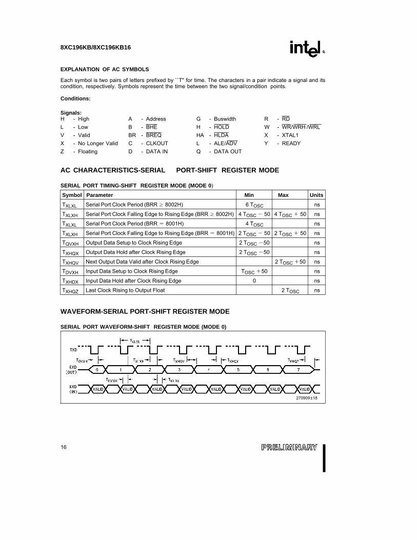
AC CHARACTERISTICS-SERIAL PORT-SHIFT REGISTER MODE
SERIAL PORT TIMING-SHIFT REGISTER MODE (MODE 0)
Symbol Parameter Min Max Units
TXLXL Serial Port Clock Period (BRR t 8002H) 6 TOSC ns
TXLXH Serial Port Clock Falling Edge to Rising Edge (BRR t 8002H) 4 TOSC b 50 4 TOSC a 50 ns
TXLXL Serial Port Clock Period (BRR e 8001H) 4 TOSC ns
TXLXH Serial Port Clock Falling Edge to Rising Edge (BRR e 8001H) 2 TOSC b 50 2 TOSC a 50 ns
TQVXH Output Data Setup to Clock Rising Edge 2 TOSC b50 ns
TXHQX Output Data Hold after Clock Rising Edge 2 TOSC b50 ns
TXHQV Next Output Data Valid after Clock Rising Edge 2 TOSC a50 ns
TDVXH Input Data Setup to Clock Rising Edge TOSC a50 ns
TXHDX Input Data Hold after Clock Rising Edge 0 ns
TXHQZ Last Clock Rising to Output Float 2 TOSC ns
WAVEFORM-SERIAL PORT-SHIFT REGISTER MODE
SERIAL PORT WAVEFORM-SHIFT REGISTER MODE (MODE 0)
270909±18
16
8XC196KB/8XC196KB16
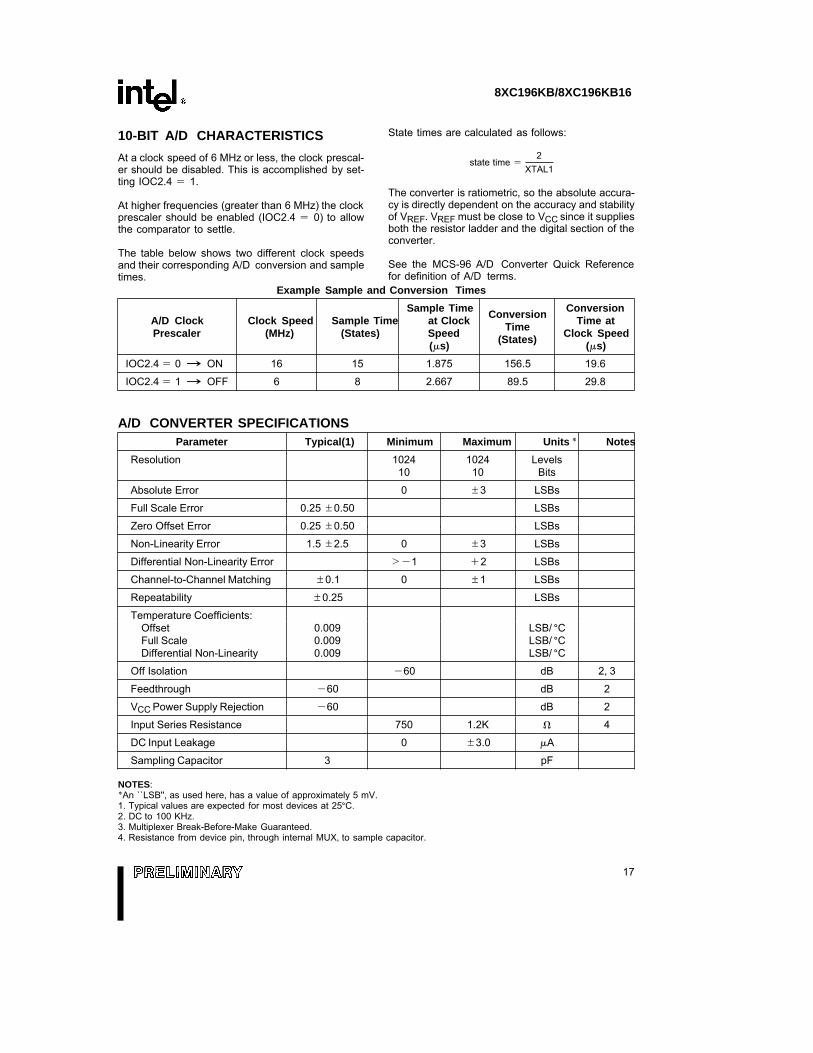
10-BIT A/D CHARACTERISTICSAt a clock speed of 6 MHz or less, the clock prescal-er should be disabled. This is accomplished by set-ting IOC2.4 e 1.
At higher frequencies (greater than 6 MHz) the clockprescaler should be enabled (IOC2.4 e 0) to allowthe comparator to settle.
The table below shows two different clock speedsand their corresponding A/D conversion and sampletimes.
State times are calculated as follows:
state time e
2XTAL1
The converter is ratiometric, so the absolute accura-cy is directly dependent on the accuracy and stabilityof VREF. VREF must be close to VCC since it suppliesboth the resistor ladder and the digital section of theconverter.
See the MCS-96 A/D Converter Quick Referencefor definition of A/D terms.
Example Sample and Conversion TimesSample Time Conversion Conversion
A/D Clock Clock Speed Sample Time at Clock Time Time atPrescaler (MHz) (States) Speed (States) Clock Speed
(ms) (ms)IOC2.4 e 0 x ON 16 15 1.875 156.5 19.6
IOC2.4 e 1 x OFF 6 8 2.667 89.5 29.8
A/D CONVERTER SPECIFICATIONSParameter Typical(1) Minimum Maximum Units * Notes
Resolution 1024 1024 Levels10 10 Bits
Absolute Error 0 g3 LSBs
Full Scale Error 0.25 g0.50 LSBs
Zero Offset Error 0.25 g0.50 LSBs
Non-Linearity Error 1.5 g2.5 0 g3 LSBs
Differential Non-Linearity Error lb1 a2 LSBs
Channel-to-Channel Matching g0.1 0 g1 LSBs
Repeatability g0.25 LSBs
Temperature Coefficients:Offset 0.009 LSB/ §CFull Scale 0.009 LSB/ §CDifferential Non-Linearity 0.009 LSB/ §C
Off Isolation b60 dB 2, 3
Feedthrough b60 dB 2
VCC Power Supply Rejection b60 dB 2
Input Series Resistance 750 1.2K X 4
DC Input Leakage 0 g3.0 mA
Sampling Capacitor 3 pF
NOTES:*An ``LSB'', as used here, has a value of approximately 5 mV.1. Typical values are expected for most devices at 25§C.2. DC to 100 KHz.3. Multiplexer Break-Before-Make Guaranteed.4. Resistance from device pin, through internal MUX, to sample capacitor.
17
8XC196KB/8XC196KB16
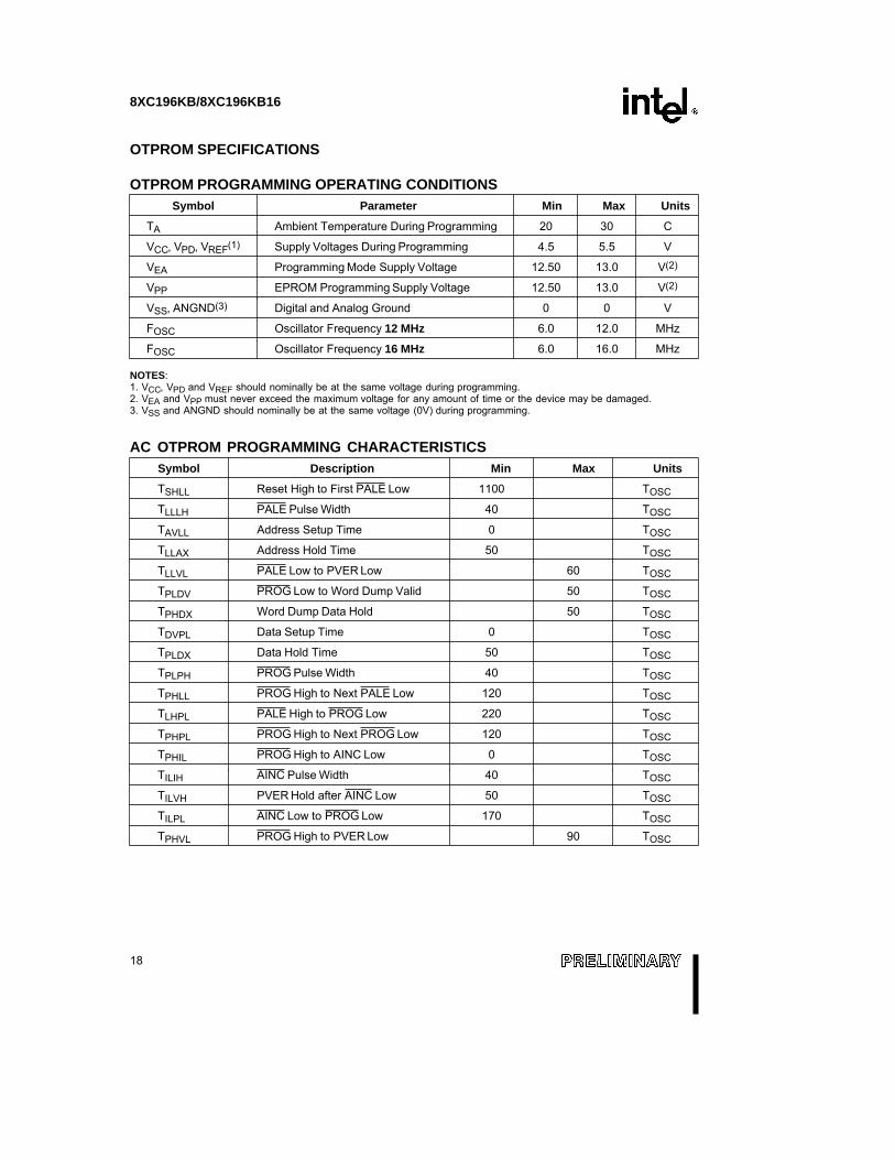
OTPROM SPECIFICATIONS
OTPROM PROGRAMMING OPERATING CONDITIONSSymbol Parameter Min Max Units
TA Ambient Temperature During Programming 20 30 C
VCC, VPD, VREF(1) Supply Voltages During Programming 4.5 5.5 V
VEA Programming Mode Supply Voltage 12.50 13.0 V(2)
VPP EPROM Programming Supply Voltage 12.50 13.0 V(2)
VSS, ANGND(3) Digital and Analog Ground 0 0 V
FOSC Oscillator Frequency 12 MHz 6.0 12.0 MHz
FOSC Oscillator Frequency 16 MHz 6.0 16.0 MHz
NOTES:1. VCC, VPD and VREF should nominally be at the same voltage during programming.2. VEA and VPP must never exceed the maximum voltage for any amount of time or the device may be damaged.3. VSS and ANGND should nominally be at the same voltage (0V) during programming.
AC OTPROM PROGRAMMING CHARACTERISTICSSymbol Description Min Max Units
TSHLL Reset High to First PALE Low 1100 TOSC
TLLLH PALE Pulse Width 40 TOSC
TAVLL Address Setup Time 0 TOSC
TLLAX Address Hold Time 50 TOSC
TLLVL PALE Low to PVER Low 60 TOSC
TPLDV PROG Low to Word Dump Valid 50 TOSC
TPHDX Word Dump Data Hold 50 TOSC
TDVPL Data Setup Time 0 TOSC
TPLDX Data Hold Time 50 TOSC
TPLPH PROG Pulse Width 40 TOSC
TPHLL PROG High to Next PALE Low 120 TOSC
TLHPL PALE High to PROG Low 220 TOSC
TPHPL PROG High to Next PROG Low 120 TOSC
TPHIL PROG High to AINC Low 0 TOSC
TILIH AINC Pulse Width 40 TOSC
TILVH PVER Hold after AINC Low 50 TOSC
TILPL AINC Low to PROG Low 170 TOSC
TPHVL PROG High to PVER Low 90 TOSC
18
8XC196KB/8XC196KB16
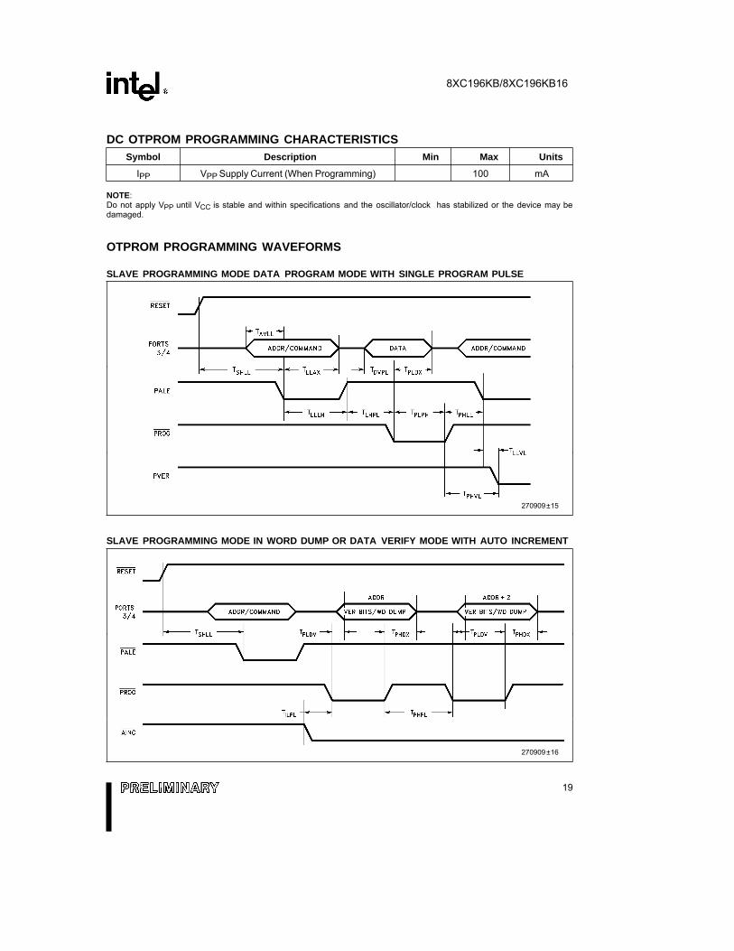
DC OTPROM PROGRAMMING CHARACTERISTICSSymbol Description Min Max Units
IPP VPP Supply Current (When Programming) 100 mA
NOTE:Do not apply VPP until VCC is stable and within specifications and the oscillator/clock has stabilized or the device may bedamaged.
OTPROM PROGRAMMING WAVEFORMS
SLAVE PROGRAMMING MODE DATA PROGRAM MODE WITH SINGLE PROGRAM PULSE
270909±15
SLAVE PROGRAMMING MODE IN WORD DUMP OR DATA VERIFY MODE WITH AUTO INCREMENT
270909±16
19
8XC196KB/8XC196KB16
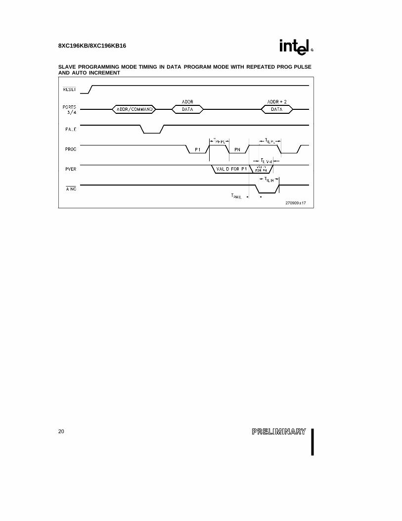
SLAVE PROGRAMMING MODE TIMING IN DATA PROGRAM MODE WITH REPEATED PROG PULSEAND AUTO INCREMENT
270909±17
20
8XC196KB/8XC196KB16
FUNCTIONAL DEVIATIONSDevices marked with an ‘‘E’’, ‘‘F’’ or ‘‘G’’ have thefollowing errata.
1. Missed Interrupt on P0.7, EXTINT
Interrupts occurring on P0.7 could be missed sincethe INT_PEND EXTINT bit may not be set. Seetechbit MC0893.
2. HSI_ MODE Divide-by-Eight
REVISION HISTORYThis data sheet (270909-006) is valid for deviceswith an ‘‘E’’, ‘‘F’’ or ‘‘G’’ at the end of the top sidetracking number. Data sheets are changed as newdevice information becomes available. Verify withyour local Intel sales office that you have the latestversion before finalizing a design or ordering devic-es.
The following differences exist between datasheet 270909-006 and 270909-005.1. Removed ‘‘Word Addressable Only’’ from Port 3
and 4 in Table 2.2. Removed ICC1, active mode current at 3.5 MHz.
This specification is not longer required.3. Removed TLLYV and TLLGV from waveform dia-
grams.4. The HSI errata and CMPL with R0 were removed
as this is now considered normal operation.5. The HSI_ MODE divide-by-eight errata was add-
ed to the known errata section.
The following differences exist between this datasheet (270909-005) and (270909-004).1. ITL MAX was – 650 μA (270909-004). Now ITL
MAX is – 800 μA (270909-005).2. IIL2 was named IIL1 (270909-004). Now IIL2 is
correctly named (270909-005).3. IIL1 was omitted (270909-004). IIL1 MAX was
added. IIL1 MAX is – 850 μA (270909-005).4. TLLYV and TLLGV (270909-004) were removed.
These timings are not required in high-speed sys-tem designs.
5. An errata was added to the known errata section.There is a possibility to miss an external interrupton P0.7 EXTINT.
The following differences exist between this datasheet (270909-004) and (270909-003).1. The ROM (80C196KB), and ROMless
(83C196KB) were combined with this data sheetresulting in no specification differences.
2. The description of the prescalar bit for the A/Dhas been enhanced.
3. THAHBVMIN was – 15 ns (270909-003). NowTHAHBVMIN is – 20 ns (270909-004).
4. TXHQZMAX was 1 TOSC (270909-003). NowTXHQZMAX is 2 TOSC (270909-004). This shouldhave no impact on designs using synchronousserial mode 0.
5. The change indicators for the 80C196KB are‘‘E’’, ‘‘F’’ and ‘‘G’’. Previously there was only onechange indicator ‘‘E’’. The change indicator isused for tracking purposes. The change indicatoris the last character in the FPO number. The FPOnumber is the second line on the top side of thedevice.
21
The following differences exist between this datasheet (270909-007) and (270909-006).1. Package prefix variables have changed. These variables are now indicated by “x”.
8XC196KB/8XC196KB16
The following differences exist between (-003) andversion (-002).1. The 12 MHz and 16 MHz devices were com-
bined in this data sheet. The 87C196KB 12 MHzonly data sheet (272035-001) is now obsolete.
2. Changes were made to the format of the datasheet and the SFR descriptions were removed.
3. The -002 version of this data sheet was valid fordevices marked with a ``B'' or a ``D'' at the endof the top side tracking number.
4. The OSCILLATOR errata was removed.5. An errata was not documented in the -002 data
sheet for devices marked with a ``B'' or a ``D''.This is the DIVIDE DURING HOLD/READY er-rata. When HOLD or READY is active and DIV/DIVB is the last instruction in the queue, the di-vide result may be incorrect.
6. TXCH was changed from Min e 40 ns to Min e
20 ns.7. TRLCL was changed from Min e 5 ns to Min e
4 ns.9. IIL1 was changed from Max e b6 mA to Max e
b7 mA.10. THAHBV was changed from Min e b10 ns to
Min e b15 ns.
Differences between the -002 and -001 data sheets.1. The -001 version of this data sheet was valid for
devices marked with a ``C'' at the end of the topside tracking number.
2. Added 64L SDIP and 80L QFP packages.3. Added IIH1.4. Changed TCHWH Min from b 10 ns to b 5 ns.5. Changed TCHWH Max from a 10 ns to a 15 ns.6. Changed TWLWH Min from TOSC b 20 ns to
TOSC b 15 ns.7. Changed TWHQX Min from TOSC b 10 ns to
TOSC b 15 ns.8. Changed TWHLH Min from TOSC b 10 ns to
TOSC b 15 ns.9. Changed TWHLH Max from TOSC a 15 ns to
TOSC a 10 ns.10. Changed TWHBX Min from TOSC b 10 ns to
TOSC b 15 ns.11. Changed THVCH Min from 85 ns to 55 ns.12. Remove THVCH Max.13. Changed TCLHAL Min from b 10 ns to b 15 ns.14. Changed TCLHAL Max from 20 ns to 15 ns.15. Changed TCLBRL Min from b 10 ns to b 15 ns.16. Changed TCLBRL Max from 20 ns to 15 ns.17. Changed THAHAX Min from b 10 ns to b 15 ns.18. Added HSI description to Functional Deviations.19. Added Oscillator description to Functional Devi-
ations.
22