Embed Size (px)
Citation preview
2
Registers • Registers are clocked sequential circuits
• A register is a group of flip-flops
– Each flip-flop capable of storing one bit of information
– An n-bit register
• consists of n flip-flops
• capable of storing n bits of information
– besides flip-flops, a register usually contains combinational logic to perform some simple tasks
– In summary
• flip-flops to hold information
• combinational logic to control the state transition
3
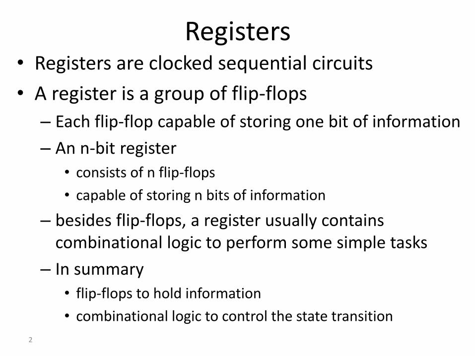
Counters • A counter is essentially a register that goes through a
predetermined sequence of states • “Counting sequence”
Register FF0 FF1 FFn-1
Combinational logic
4
Uses of Registers and Counters • Registers are useful for storing and manipulating
information
– internal registers in microprocessors to manipulate data
• Counters are extensively used in control logic
– PC (program counter) in microprocessors
5
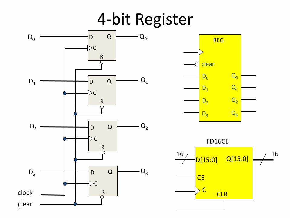
4-bit Register REG
Q3
Q2
Q1
Q0
D3
D2
D1
D0
clear
D Q
clock
C
R
D Q
C
R
D Q
C
R
D Q
C
R
clear
D0
D1
D2
D3
Q0
Q1
Q2
Q3
FD16CE
16 16 D[15:0] Q[15:0]
CE
C CLR
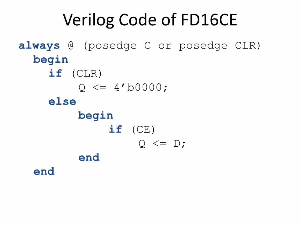
Verilog Code of FD16CE
always @ (posedge C or posedge CLR)
begin
if (CLR)
Q <= 4’b0000;
else
begin
if (CE)
Q <= D;
end
end
7
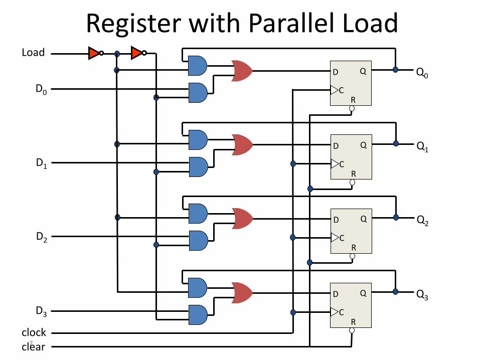
Register with Parallel Load Load
D Q
C R
Q0
D Q
C R
Q1
D Q
C R
Q2
D Q
C R
Q3
clock
clear
D1
D2
D3
D0
8
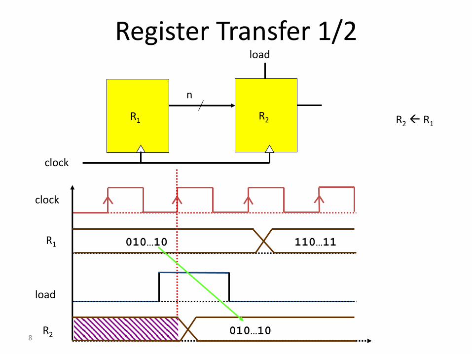
Register Transfer 1/2
R1 R2
n
load
clock
load
clock
R2 R1
R1 010…10 110…11
010…10 R2
9
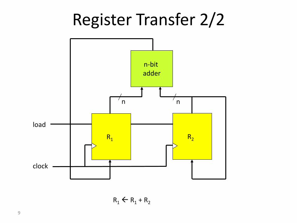
Register Transfer 2/2
R1 R1 + R2
clock
R1 R2
n
n-bit adder
n
load
10
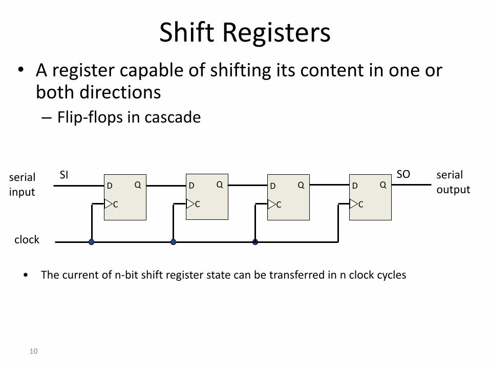
Shift Registers • A register capable of shifting its content in one or
both directions – Flip-flops in cascade
serial input
serial output D Q
C
SI D Q
C
D Q
C
D Q
C
SO
clock
• The current of n-bit shift register state can be transferred in n clock cycles
11
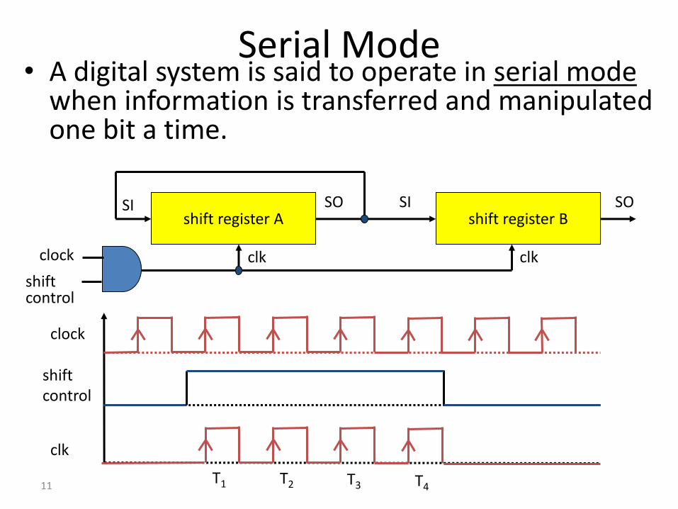
Serial Mode • A digital system is said to operate in serial mode
when information is transferred and manipulated one bit a time.
shift register A shift register B SO SI SI SO
clk clk clock
shift control
clock
shift control
clk
T1 T2 T3 T4
12
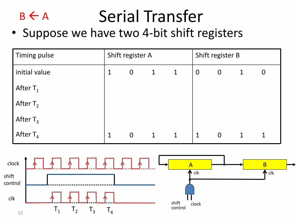
Serial Transfer • Suppose we have two 4-bit shift registers
1 1 0 1 1 1 0 1 After T4
After T3
After T2
After T1
0 1 0 0 1 1 0 1 initial value
Shift register B Shift register A Timing pulse
B A
clock
shift control
clk
T1 T2 T3 T4
A B clk clk
clock shift control
13
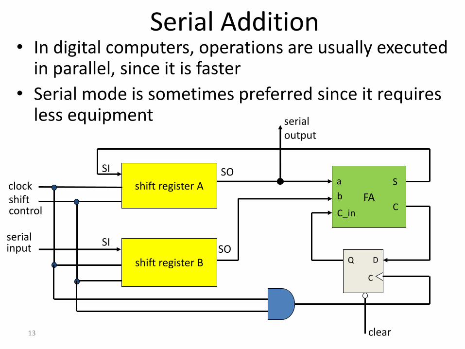
Serial Addition • In digital computers, operations are usually executed
in parallel, since it is faster
• Serial mode is sometimes preferred since it requires less equipment
shift register A
shift register B
SI
FA
a
b
C_in
S
C
D Q
C
SO
SO
SI serial input
clock shift control
clear
serial output
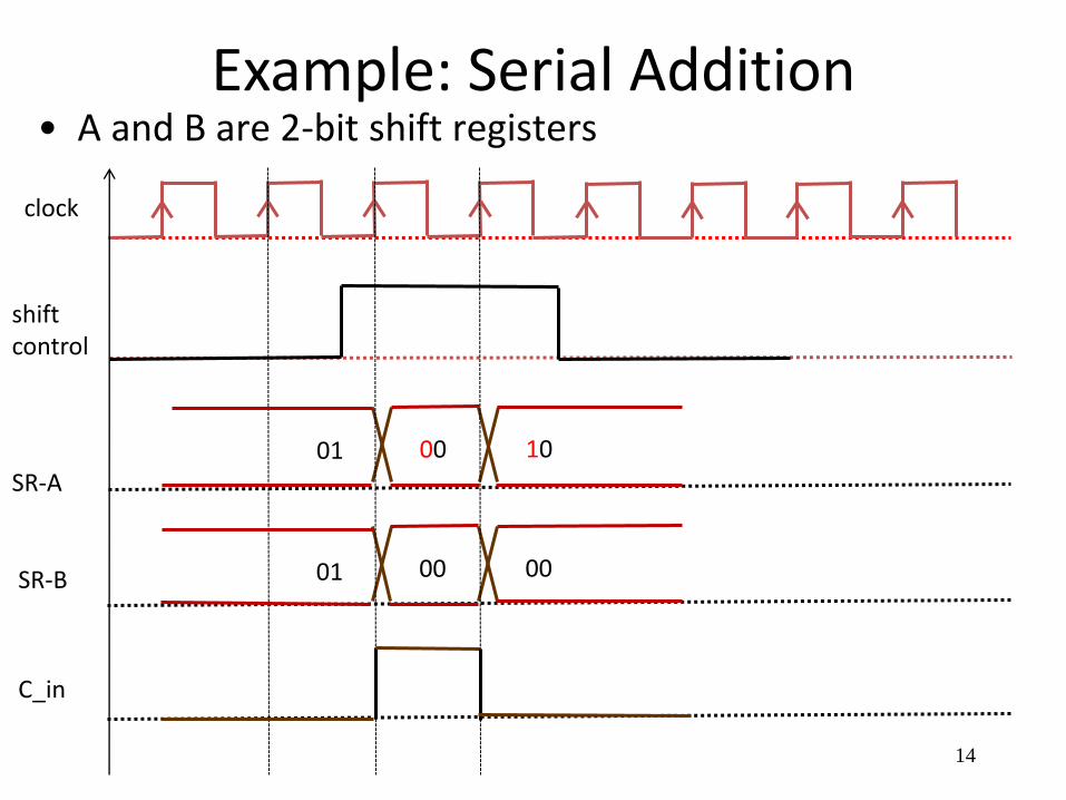
Example: Serial Addition
14
• A and B are 2-bit shift registers
clock
00 10
00 00
shift control
SR-A
SR-B
C_in
01
01
15
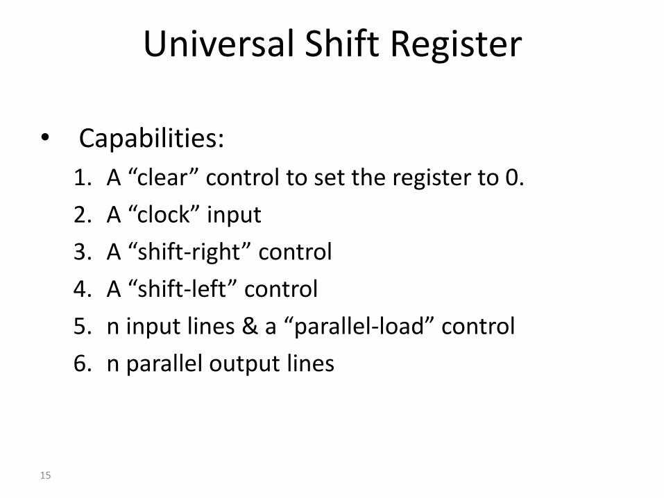
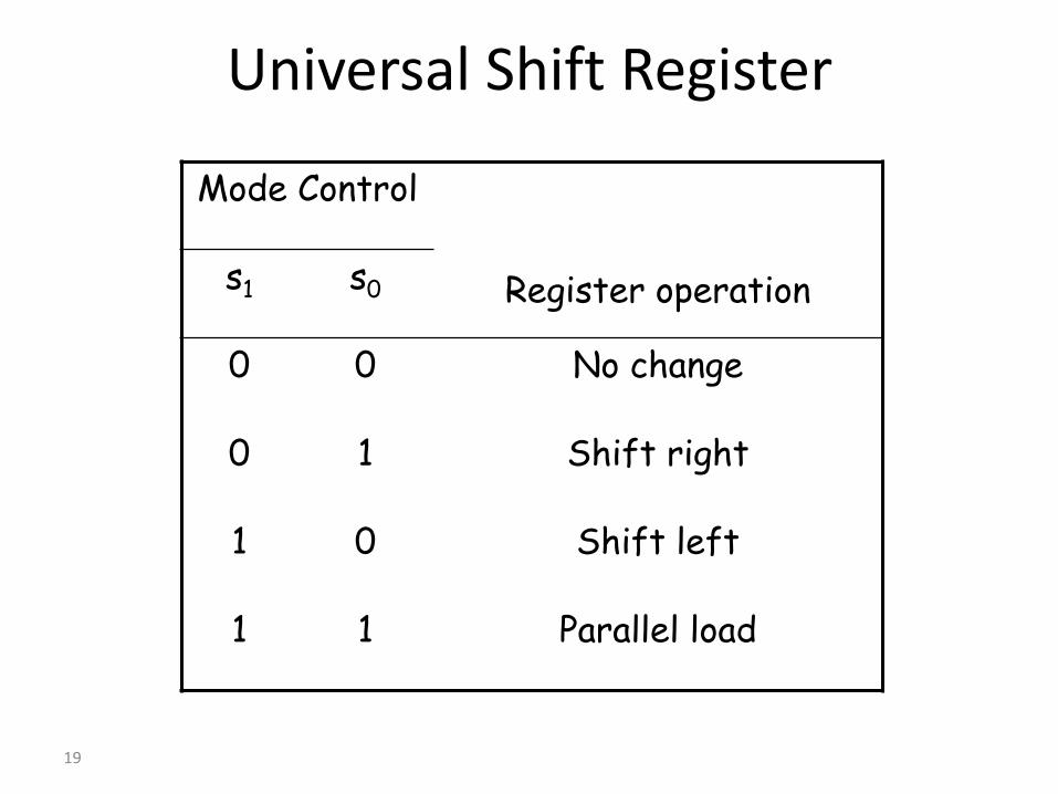
Universal Shift Register
• Capabilities:
1. A “clear” control to set the register to 0.
2. A “clock” input
3. A “shift-right” control
4. A “shift-left” control
5. n input lines & a “parallel-load” control
6. n parallel output lines
16
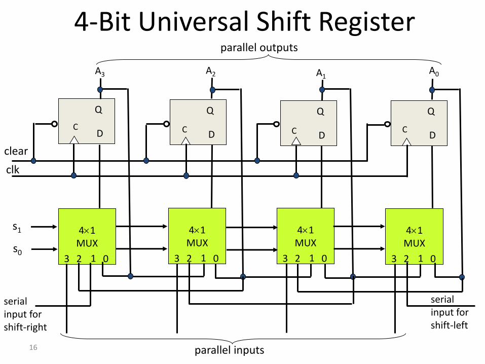
4-Bit Universal Shift Register
D
Q
C D
Q
C D
Q
C D
Q
C
A0 A1 A2 A3
parallel outputs
clear
clk
41 MUX
0 1 2 3
41 MUX
0 1 2 3
41 MUX
0 1 2 3
41 MUX
0 1 2 3
s1
s0
serial input for shift-right
serial input for shift-left
parallel inputs
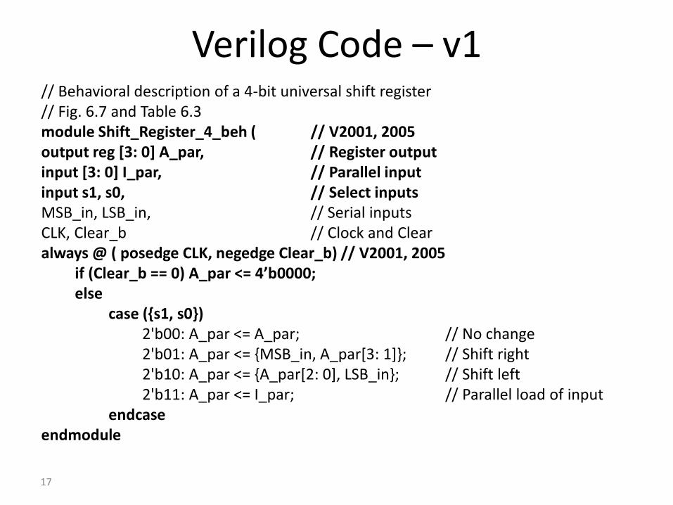
Verilog Code – v1 // Behavioral description of a 4-bit universal shift register // Fig. 6.7 and Table 6.3 module Shift_Register_4_beh ( // V2001, 2005 output reg [3: 0] A_par, // Register output input [3: 0] I_par, // Parallel input input s1, s0, // Select inputs MSB_in, LSB_in, // Serial inputs CLK, Clear_b // Clock and Clear always @ ( posedge CLK, negedge Clear_b) // V2001, 2005
if (Clear_b == 0) A_par <= 4’b0000; else
case ({s1, s0}) 2'b00: A_par <= A_par; // No change 2'b01: A_par <= {MSB_in, A_par[3: 1]}; // Shift right 2'b10: A_par <= {A_par[2: 0], LSB_in}; // Shift left 2'b11: A_par <= I_par; // Parallel load of input
endcase endmodule
17
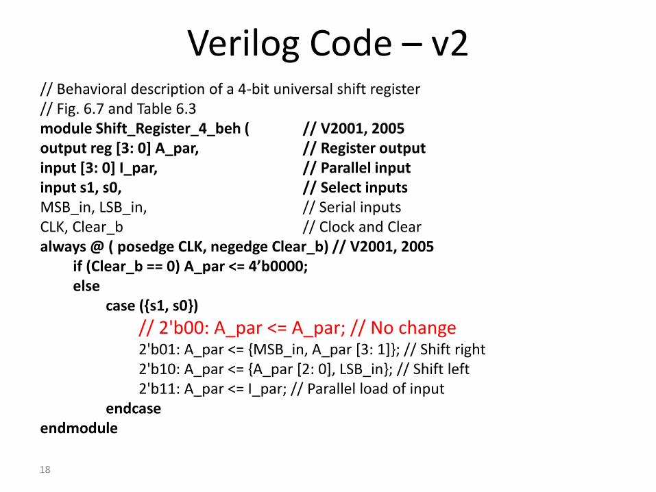
Verilog Code – v2 // Behavioral description of a 4-bit universal shift register // Fig. 6.7 and Table 6.3 module Shift_Register_4_beh ( // V2001, 2005 output reg [3: 0] A_par, // Register output input [3: 0] I_par, // Parallel input input s1, s0, // Select inputs MSB_in, LSB_in, // Serial inputs CLK, Clear_b // Clock and Clear always @ ( posedge CLK, negedge Clear_b) // V2001, 2005
if (Clear_b == 0) A_par <= 4’b0000; else
case ({s1, s0})
// 2'b00: A_par <= A_par; // No change 2'b01: A_par <= {MSB_in, A_par [3: 1]}; // Shift right 2'b10: A_par <= {A_par [2: 0], LSB_in}; // Shift left 2'b11: A_par <= I_par; // Parallel load of input
endcase endmodule
18
19
Universal Shift Register
Mode Control
Register operation s1 s0
0 0 No change
0 1 Shift right
1 0 Shift left
1 1 Parallel load
20
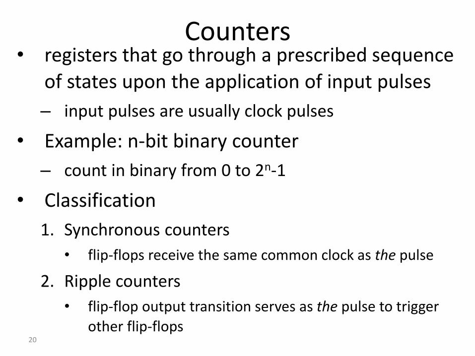
Counters • registers that go through a prescribed sequence
of states upon the application of input pulses
– input pulses are usually clock pulses
• Example: n-bit binary counter
– count in binary from 0 to 2n-1
• Classification
1. Synchronous counters
• flip-flops receive the same common clock as the pulse
2. Ripple counters
• flip-flop output transition serves as the pulse to trigger
other flip-flops
21
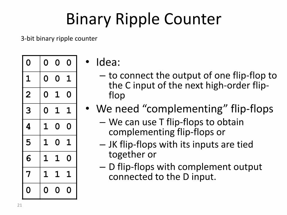
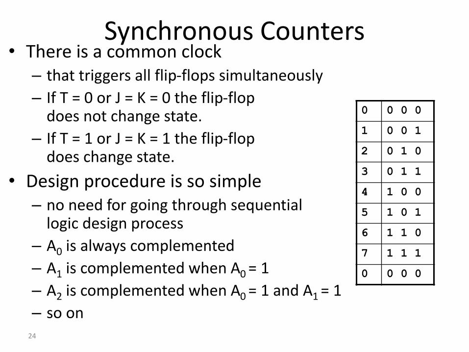
Binary Ripple Counter
0 0 0 0
1 0 0 1
2 0 1 0
3 0 1 1
4 1 0 0
5 1 0 1
6 1 1 0
7 1 1 1
0 0 0 0
3-bit binary ripple counter
• Idea: – to connect the output of one flip-flop to
the C input of the next high-order flip-flop
• We need “complementing” flip-flops – We can use T flip-flops to obtain
complementing flip-flops or – JK flip-flops with its inputs are tied
together or – D flip-flops with complement output
connected to the D input.
22
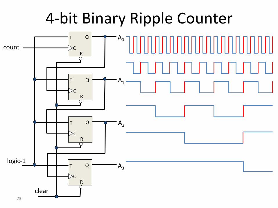
4-bit Binary Ripple Counter T Q
C R
A0
T Q
C R
A1
T Q
C R
A2
T Q
C R
A3
clear
count
logic-1
D Q
C R
A0
D Q
C R
A1
D Q
C R
A2
D Q
C R
A3
clear
count
0 0 0 0 0
1 0 0 0 1
2 0 0 1 0
3 0 0 1 1
4 0 1 0 0
5 0 1 0 1
6 0 1 1 0
7 0 1 1 1
8 1 0 0 0
9 1 0 0 1
10 1 0 1 0
11 1 0 1 1
12 1 1 0 0
13 1 1 0 1
14 1 1 1 0
15 1 1 1 1
0 0 0 0 0
23
4-bit Binary Ripple Counter T Q
C R
A0
T Q
C R
A1
T Q
C R
A2
T Q
C R
A3
clear
count
logic-1
24
Synchronous Counters • There is a common clock
– that triggers all flip-flops simultaneously
– If T = 0 or J = K = 0 the flip-flop does not change state.
– If T = 1 or J = K = 1 the flip-flop does change state.
• Design procedure is so simple – no need for going through sequential
logic design process
– A0 is always complemented
– A1 is complemented when A0 = 1
– A2 is complemented when A0 = 1 and A1 = 1
– so on
0 0 0 0
1 0 0 1
2 0 1 0
3 0 1 1
4 1 0 0
5 1 0 1
6 1 1 0
7 1 1 1
0 0 0 0
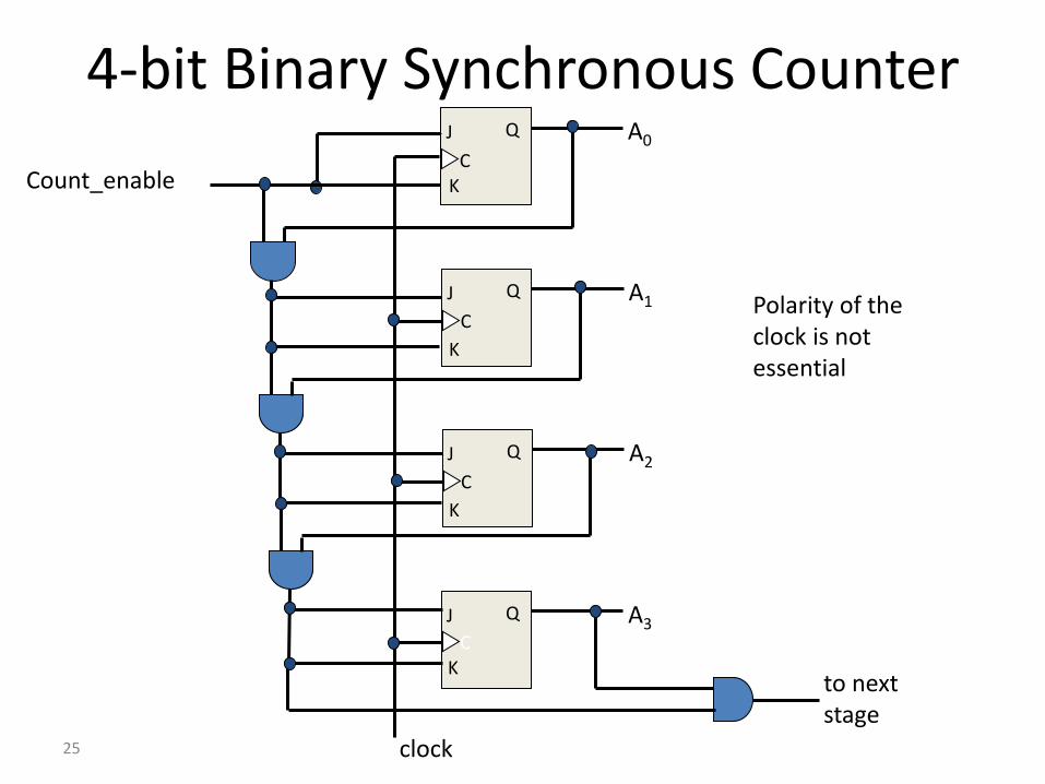
25
4-bit Binary Synchronous Counter J Q
C
A0
J Q
C
A1
J Q
C
A2
J Q
C
A3
K
K
K
K
clock
Count_enable
to next stage
Polarity of the clock is not essential
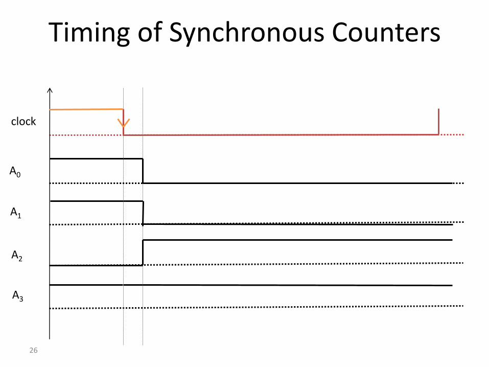
Timing of Synchronous Counters
26
A0
clock
A3
A1
A2
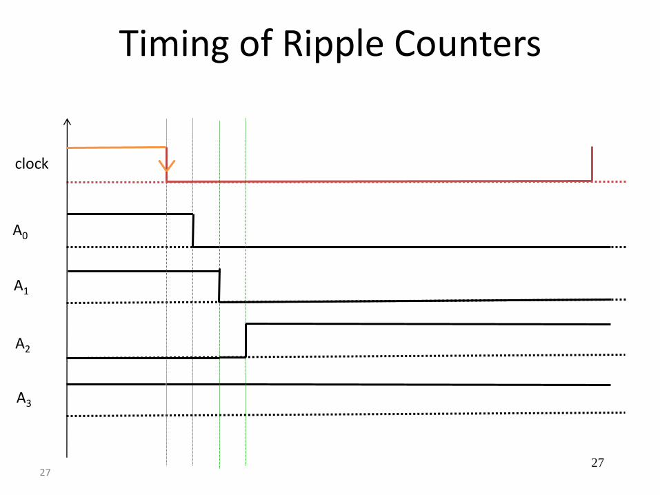
Timing of Ripple Counters
27 27
A0
clock
A3
A1
A2
28
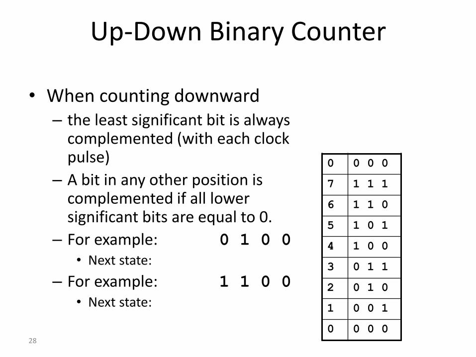
Up-Down Binary Counter
• When counting downward – the least significant bit is always
complemented (with each clock pulse)
– A bit in any other position is complemented if all lower significant bits are equal to 0.
– For example: 0 1 0 0
• Next state:
– For example: 1 1 0 0
• Next state:
0 0 0 0
7 1 1 1
6 1 1 0
5 1 0 1
4 1 0 0
3 0 1 1
2 0 1 0
1 0 0 1
0 0 0 0
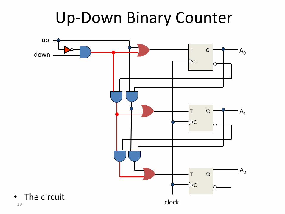
29
Up-Down Binary Counter
• The circuit
T Q
C
A0
T Q
C
A1
T Q
C
A2
C clock
up
down
30
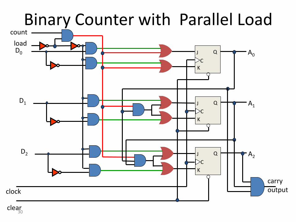
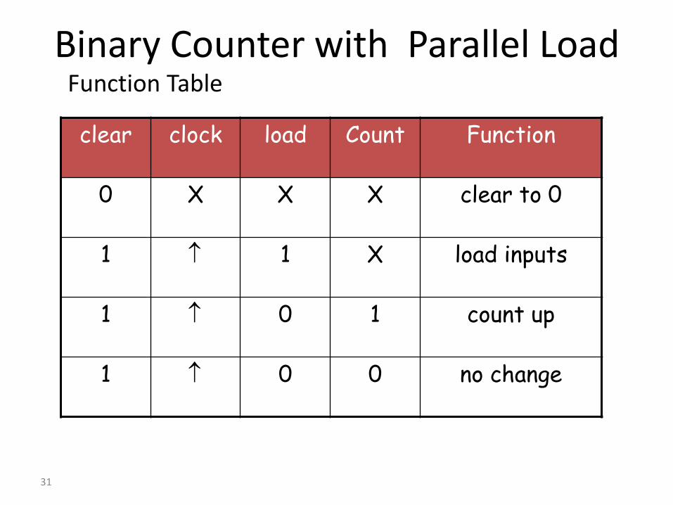
Binary Counter with Parallel Load
J Q
C
A0
J Q
C
A1
J Q
C
A2
K
K
K
clock
clear
count
load D0
D1
D2
carry output
31
Binary Counter with Parallel Load
clear clock load Count Function
0 X X X clear to 0
1 1 X load inputs
1 0 1 count up
1 0 0 no change
Function Table
32
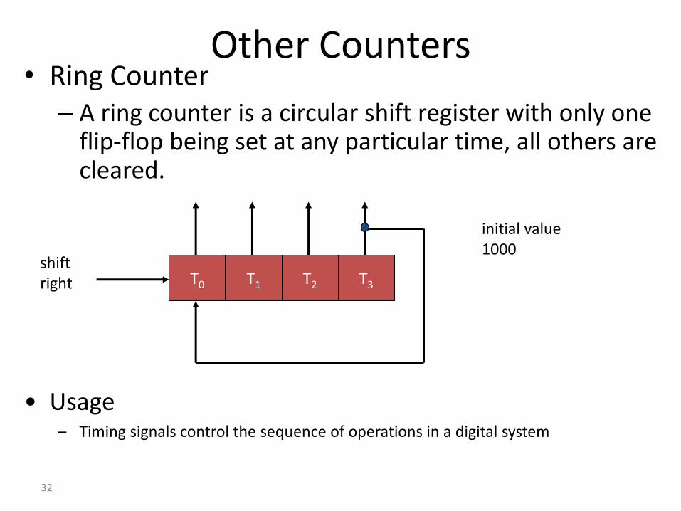
Other Counters • Ring Counter
– A ring counter is a circular shift register with only one flip-flop being set at any particular time, all others are cleared.
shift right T0 T1 T2 T3
initial value 1000
• Usage – Timing signals control the sequence of operations in a digital system
33
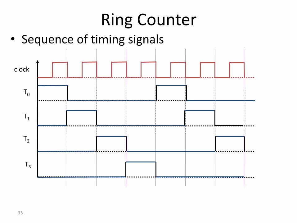
Ring Counter • Sequence of timing signals
clock
T0
T1
T2
T3
34
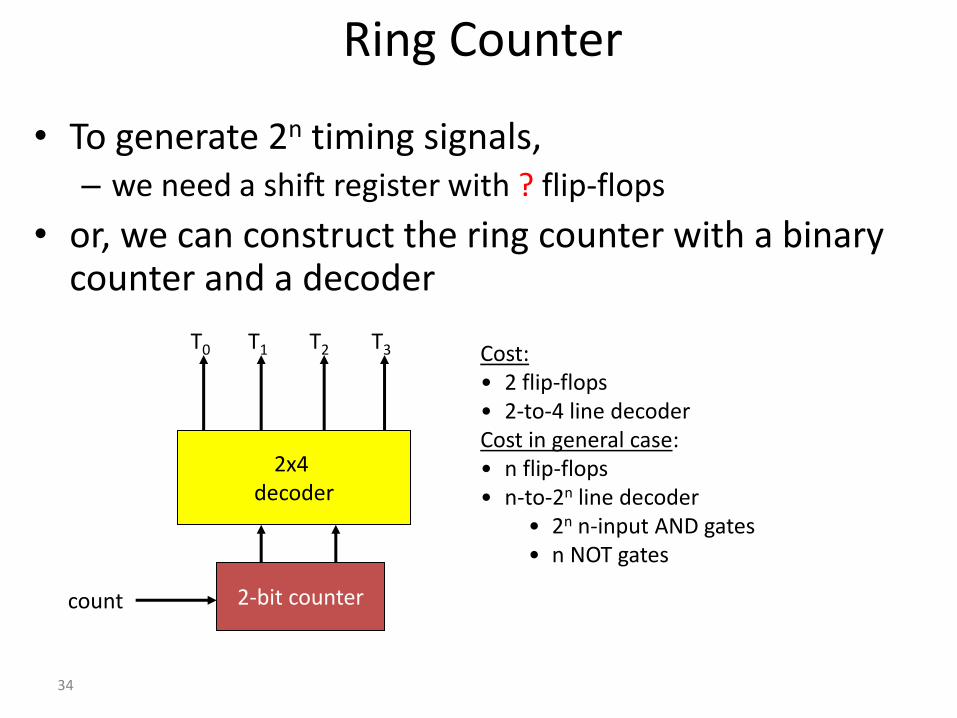
Ring Counter
• To generate 2n timing signals, – we need a shift register with ? flip-flops
• or, we can construct the ring counter with a binary counter and a decoder
2x4 decoder
T0 T1 T2 T3
2-bit counter count
Cost: • 2 flip-flops • 2-to-4 line decoder Cost in general case: • n flip-flops • n-to-2n line decoder
• 2n n-input AND gates • n NOT gates
35
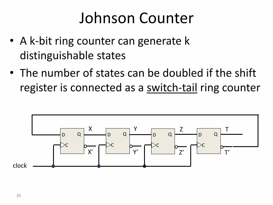
Johnson Counter
• A k-bit ring counter can generate k distinguishable states
• The number of states can be doubled if the shift register is connected as a switch-tail ring counter
clock
D Q
C
D Q
C
D Q
C
D Q
C
X
X’
Y
Y’
Z
Z’
T
T’
36
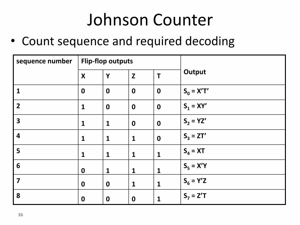
Johnson Counter • Count sequence and required decoding
S7 = Z’T
S6 = Y’Z
S5 = X’Y
S4 = XT
S3 = ZT’
S2 = YZ’
S1 = XY’
S0 = X’T’ 0 0 0 0
8
7
6
5
4
3
2
1
T Z Y X
Output
Flip-flop outputs sequence number
0 0 0 1
0 0 1 1
0 1 1 1
1 1 1 1
1 1 1 0
1 1 0 0
1 0 0 0
37
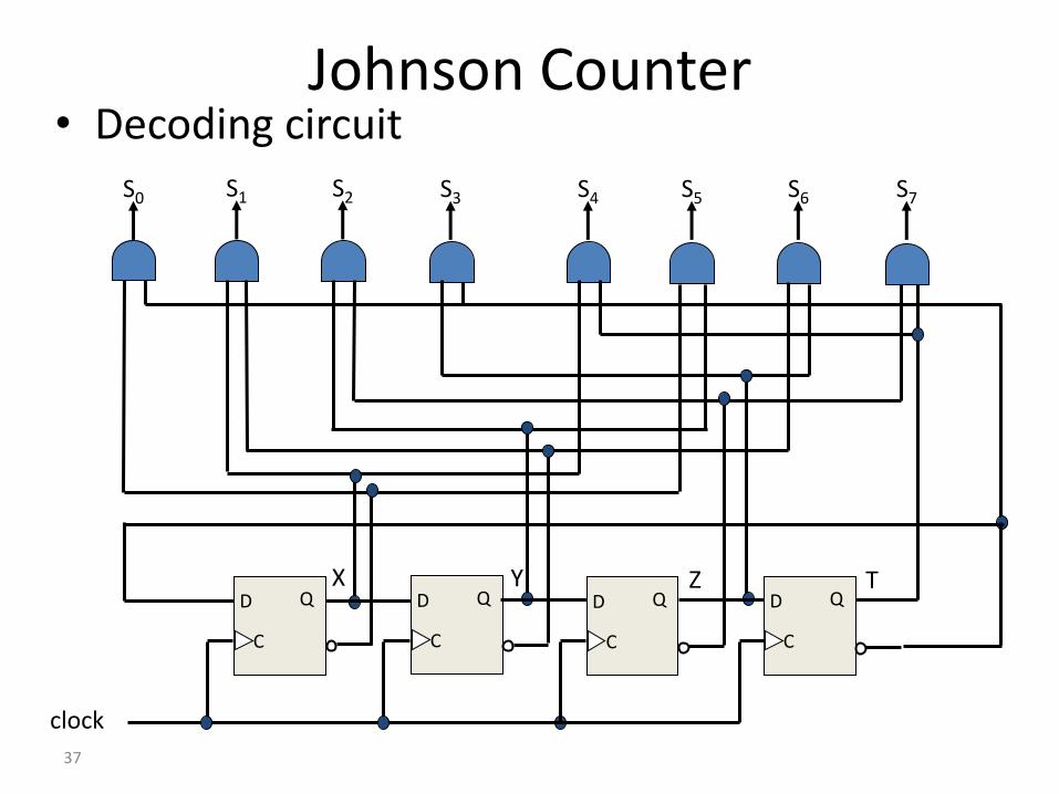
Johnson Counter • Decoding circuit
S0 S1 S2 S3 S4 S5 S6 S7
clock
D Q
C
D Q
C
D Q
C
D Q
C
X Y Z T
38
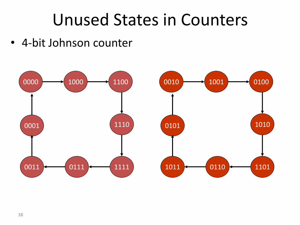
Unused States in Counters • 4-bit Johnson counter
0000 1000 1100
1110
1111 0111 0011
0001
0010 1001 0100
1010
1101 0110 1011
0101
39
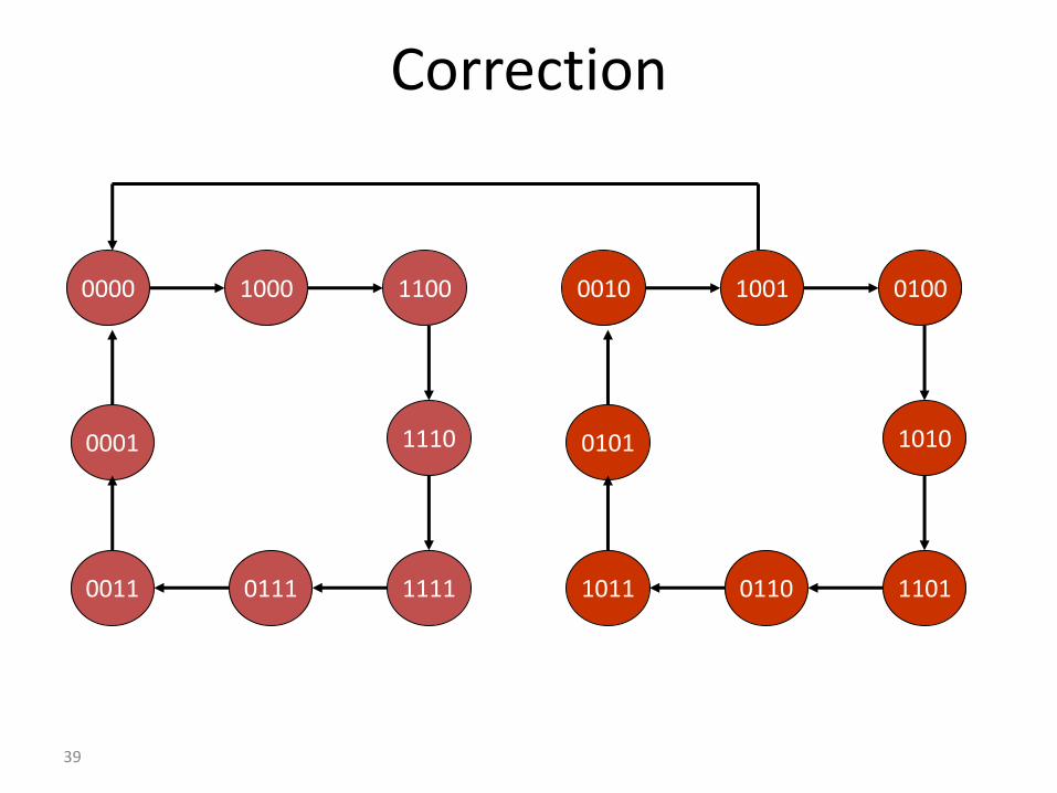
Correction
0000 1000 1100
1110
1111 0111 0011
0001
0010 1001 0100
1010
1101 0110 1011
0101
40
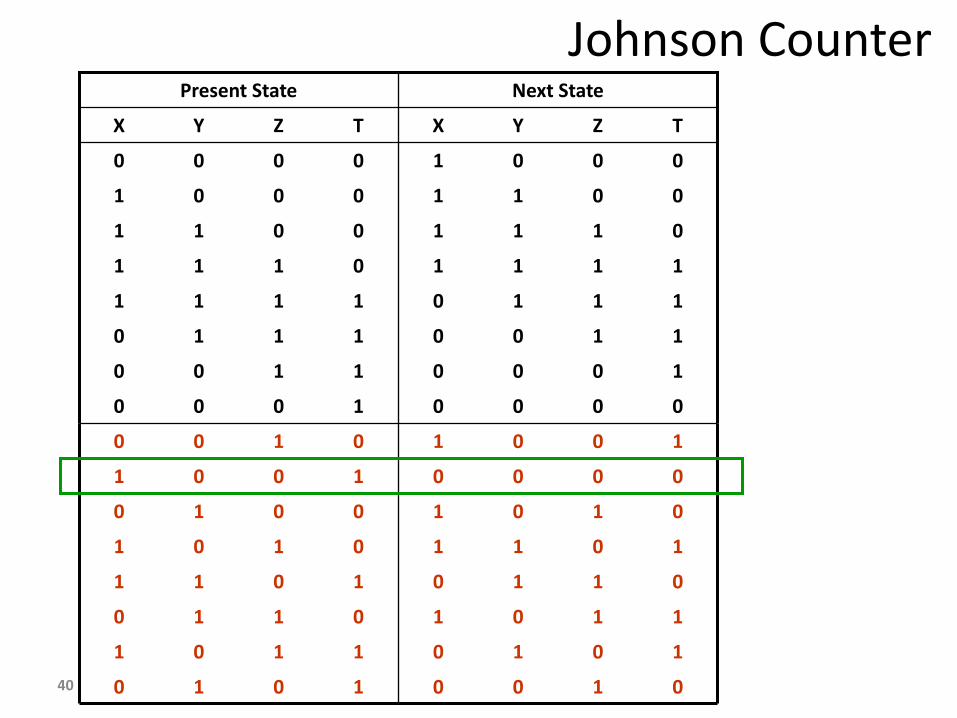
Johnson Counter
0 1 0 0 1 0 1 0
1 0 1 0 1 1 0 1
1 1 0 1 0 1 1 0
0 1 1 0 1 0 1 1
1 0 1 1 0 1 0 1
0 1 0 1 0 0 1 0
0 0 0 0 1 0 0 1
1 0 0 1 0 1 0 0
Next State Present State
0 0 0 0 1 0 0 0
1 0 0 0 1 1 0 0
1 1 0 0 1 1 1 0
1 1 1 0 1 1 1 1
1 1 1 1 0 1 1 1
0 1 1 1 0 0 1 1
0 0 1 1 0 0 0 1
0 0 0 1 0 0 0 0
T Z Y X T Z Y X
41
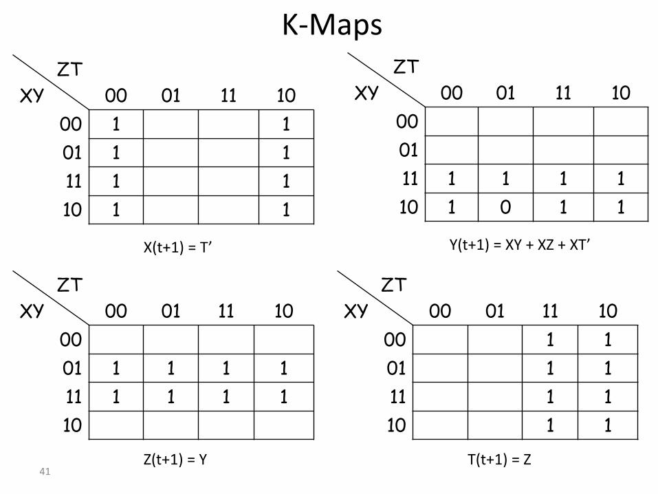
K-Maps ZT
XY
00
01
11
10
00 1 1
01 1 1
11 1 1
10 1 1
X(t+1) = T’
ZT
XY
00
01
11
10
00
01
11 1 1 1 1
10 1 0 1 1
Y(t+1) = XY + XZ + XT’
ZT
XY
00
01
11
10
00
01 1 1 1 1
11 1 1 1 1
10
Z(t+1) = Y
ZT
XY
00
01
11
10
00 1 1
01 1 1
11 1 1
10 1 1
T(t+1) = Z
42
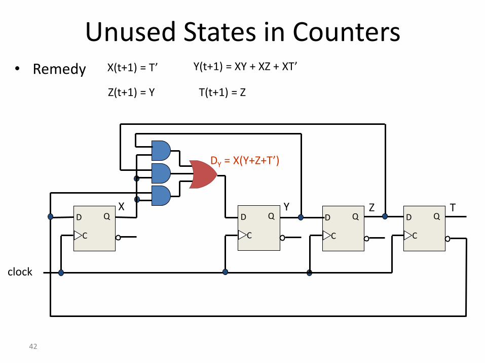
Unused States in Counters • Remedy
DY = X(Y+Z+T’)
X(t+1) = T’ Y(t+1) = XY + XZ + XT’
Z(t+1) = Y T(t+1) = Z
clock
Z T D Q
C
D Q
C
D Q
C
D Q
C
X Y