Embed Size (px)
Citation preview
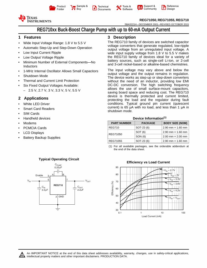
Load Current (mA)
Effic
iency (
%)
90
80
70
60
50
40
301 10 1000.1
V = VIN OUT
V = 2.7VIN
V = 4.2VIN
V = 3.6VIN
V = 3.3VIN
V = 3VIN
VIN
Enable
VOUT
GND
REG710C
IN
2.2mF
COUT
2.2mF
CPUMP
0.22mF
4 63
5 1
2
Product
Folder
Sample &Buy
Technical
Documents
Tools &
Software
Support &Community
ReferenceDesign
REG71050, REG71055, REG710SBAS221H –DECEMBER 2001–REVISED OCTOBER 2015
REG710xx Buck-Boost Charge Pump with up to 60-mA Output Current1 Features 3 Description
The REG710 family of devices are switched capacitor1• Wide Input Voltage Range: 1.8 V to 5.5 V
voltage converters that generate regulated, low-ripple• Automatic Step-Up and Step-Down Operation output voltage from an unregulated input voltage. A• Low Input Current Ripple wide input supply voltage from 1.8 V to 5.5 V makes
the REG710 family of devices ideal for a variety of• Low Output Voltage Ripplebattery sources, such as single-cell Li-Ion, or 2-cell• Minimum Number of External Components—No and 3-cell nickel-based or alkaline-based chemistries.InductorsThe input voltage may vary above and below the• 1-MHz Internal Oscillator Allows Small Capacitorsoutput voltage and the output remains in regulation.• Shutdown Mode The device works as step-up or step-down converters
• Thermal and Current Limit Protection without the need of an inductor, providing low EMIDC-DC conversion. The high switching frequency• Six Fixed Output Voltages Available:allows the use of small surface-mount capacitors,– 2.5 V, 2.7 V, 3 V, 3.3 V, 5 V, 5.5 V saving board space and reducing cost. The REG710device is thermally protected and current limited,2 Applications protecting the load and the regulator during faultconditions. Typical ground pin current (quiescent• White LED Drivercurrent) is 65 μA with no load, and less than 1 μA in• Smart Card Readers shutdown mode.
• SIM Cards• Handheld devices Device Information(1)
PART NUMBER PACKAGE BODY SIZE (NOM)• ModemsREG710 SOT-23 (6) 2.90 mm × 1.60 mm• PCMCIA Cards
SOT (6) 2.90 mm × 1.60 mm• LCD Displays REG71050SON (6) 2.00 mm × 2.00 mm• Battery Backup Supplies
REG71055 SOT-23 (6) 2.90 mm × 1.60 mm
(1) For all available packages, see the orderable addendum atthe end of the data sheet.
spacingTypical Operating Circuit
Efficiency vs Load Current
1
An IMPORTANT NOTICE at the end of this data sheet addresses availability, warranty, changes, use in safety-critical applications,intellectual property matters and other important disclaimers. PRODUCTION DATA.
REG71050, REG71055, REG710SBAS221H –DECEMBER 2001–REVISED OCTOBER 2015 www.ti.com
Table of Contents8.4 Device Functional Modes.......................................... 81 Features .................................................................. 1
9 Application and Implementation ........................ 102 Applications ........................................................... 19.1 Application Information............................................ 103 Description ............................................................. 19.2 Typical Applications ................................................ 104 Revision History..................................................... 29.3 System Examples ................................................... 145 Device Comparison Table ..................................... 3
10 Power Supply Recommendations ..................... 176 Pin Configuration and Functions ......................... 311 Layout................................................................... 177 Specifications......................................................... 3
11.1 Layout Guidelines ................................................. 177.1 Absolute Maximum Ratings ...................................... 311.2 Layout Example .................................................... 177.2 ESD Ratings.............................................................. 4
12 Device and Documentation Support ................. 187.3 Recommended Operating Conditions....................... 412.1 Device Support...................................................... 187.4 Thermal Information .................................................. 412.2 Related Links ........................................................ 187.5 Electrical Characteristics........................................... 412.3 Community Resources.......................................... 187.6 Typical Characteristics .............................................. 612.4 Trademarks ........................................................... 188 Detailed Description .............................................. 712.5 Electrostatic Discharge Caution............................ 188.1 Overview ................................................................... 712.6 Glossary ................................................................ 188.2 Functional Block Diagram ......................................... 8
13 Mechanical, Packaging, and Orderable8.3 Feature Description................................................... 8Information ........................................................... 18
4 Revision HistoryNOTE: Page numbers for previous revisions may differ from page numbers in the current version.
Changes from Revision G (January 2009) to Revision H Page
• Added ESD Ratings table, Feature Description section, Device Functional Modes, Application and Implementationsection, Power Supply Recommendations section, Layout section, Device and Documentation Support section, andMechanical, Packaging, and Orderable Information section ................................................................................................. 1
2 Submit Documentation Feedback Copyright © 2001–2015, Texas Instruments Incorporated
Product Folder Links: REG71050 REG71055 REG710
VIN
CPUMP-
VOUTCPUMP+
GND
Enable
1
2
3
6
5
4
ThermalExposed
Pad
VOUT
GND
Enable
1
2
3
6
5
4
CPUMP+
VIN
CPUMP-
REG71050, REG71055, REG710www.ti.com SBAS221H –DECEMBER 2001–REVISED OCTOBER 2015
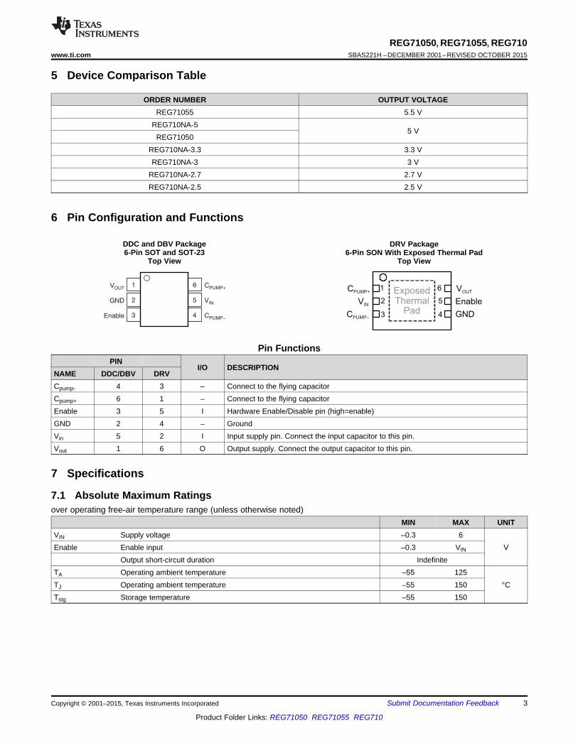
5 Device Comparison Table
ORDER NUMBER OUTPUT VOLTAGEREG71055 5.5 V
REG710NA-55 V
REG71050REG710NA-3.3 3.3 VREG710NA-3 3 V
REG710NA-2.7 2.7 VREG710NA-2.5 2.5 V
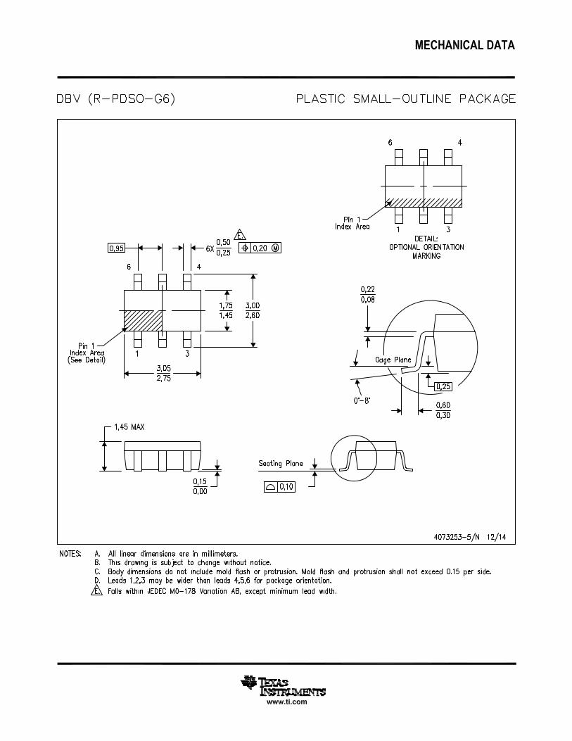
6 Pin Configuration and Functions
DDC and DBV Package DRV Package6-Pin SOT and SOT-23 6-Pin SON With Exposed Thermal Pad
Top View Top View
Pin FunctionsPIN
I/O DESCRIPTIONNAME DDC/DBV DRVCpump- 4 3 – Connect to the flying capacitorCpump+ 6 1 – Connect to the flying capacitorEnable 3 5 I Hardware Enable/Disable pin (high=enable)GND 2 4 – GroundVin 5 2 I Input supply pin. Connect the input capacitor to this pin.Vout 1 6 O Output supply. Connect the output capacitor to this pin.
7 Specifications
7.1 Absolute Maximum Ratingsover operating free-air temperature range (unless otherwise noted)
MIN MAX UNITVIN Supply voltage –0.3 6Enable Enable input –0.3 VIN V
Output short-circuit duration IndefiniteTA Operating ambient temperature –55 125TJ Operating ambient temperature –55 150 °CTstg Storage temperature –55 150
Copyright © 2001–2015, Texas Instruments Incorporated Submit Documentation Feedback 3
Product Folder Links: REG71050 REG71055 REG710
REG71050, REG71055, REG710SBAS221H –DECEMBER 2001–REVISED OCTOBER 2015 www.ti.com
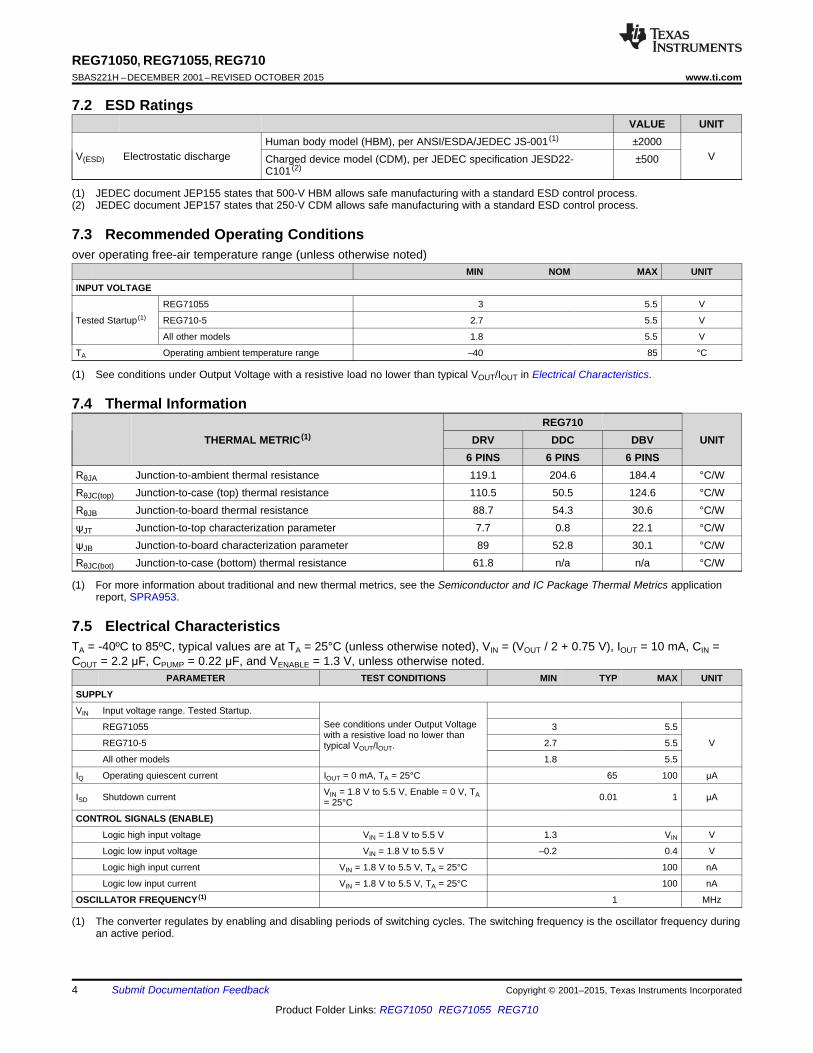
7.2 ESD RatingsVALUE UNIT
Human body model (HBM), per ANSI/ESDA/JEDEC JS-001 (1) ±2000V(ESD) Electrostatic discharge VCharged device model (CDM), per JEDEC specification JESD22- ±500
C101 (2)
(1) JEDEC document JEP155 states that 500-V HBM allows safe manufacturing with a standard ESD control process.(2) JEDEC document JEP157 states that 250-V CDM allows safe manufacturing with a standard ESD control process.
7.3 Recommended Operating Conditionsover operating free-air temperature range (unless otherwise noted)
MIN NOM MAX UNIT
INPUT VOLTAGE
REG71055 3 5.5 V
Tested Startup (1) REG710-5 2.7 5.5 V
All other models 1.8 5.5 V
TA Operating ambient temperature range –40 85 °C
(1) See conditions under Output Voltage with a resistive load no lower than typical VOUT/IOUT in Electrical Characteristics.
7.4 Thermal InformationREG710
THERMAL METRIC (1) DRV DDC DBV UNIT6 PINS 6 PINS 6 PINS
RθJA Junction-to-ambient thermal resistance 119.1 204.6 184.4 °C/WRθJC(top) Junction-to-case (top) thermal resistance 110.5 50.5 124.6 °C/WRθJB Junction-to-board thermal resistance 88.7 54.3 30.6 °C/WψJT Junction-to-top characterization parameter 7.7 0.8 22.1 °C/WψJB Junction-to-board characterization parameter 89 52.8 30.1 °C/WRθJC(bot) Junction-to-case (bottom) thermal resistance 61.8 n/a n/a °C/W
(1) For more information about traditional and new thermal metrics, see the Semiconductor and IC Package Thermal Metrics applicationreport, SPRA953.
7.5 Electrical CharacteristicsTA = -40ºC to 85ºC, typical values are at TA = 25°C (unless otherwise noted), VIN = (VOUT / 2 + 0.75 V), IOUT = 10 mA, CIN =COUT = 2.2 μF, CPUMP = 0.22 μF, and VENABLE = 1.3 V, unless otherwise noted.
PARAMETER TEST CONDITIONS MIN TYP MAX UNIT
SUPPLY
VIN Input voltage range. Tested Startup.See conditions under Output VoltageREG71055 3 5.5with a resistive load no lower than
REG710-5 2.7 5.5 Vtypical VOUT/IOUT.All other models 1.8 5.5
IQ Operating quiescent current IOUT = 0 mA, TA = 25°C 65 100 μA
VIN = 1.8 V to 5.5 V, Enable = 0 V, TAISD Shutdown current 0.01 1 μA= 25°C
CONTROL SIGNALS (ENABLE)
Logic high input voltage VIN = 1.8 V to 5.5 V 1.3 VIN V
Logic low input voltage VIN = 1.8 V to 5.5 V –0.2 0.4 V
Logic high input current VIN = 1.8 V to 5.5 V, TA = 25°C 100 nA
Logic low input current VIN = 1.8 V to 5.5 V, TA = 25°C 100 nA
OSCILLATOR FREQUENCY (1) 1 MHz
(1) The converter regulates by enabling and disabling periods of switching cycles. The switching frequency is the oscillator frequency duringan active period.
4 Submit Documentation Feedback Copyright © 2001–2015, Texas Instruments Incorporated
Product Folder Links: REG71050 REG71055 REG710

REG71050, REG71055, REG710www.ti.com SBAS221H –DECEMBER 2001–REVISED OCTOBER 2015
Electrical Characteristics (continued)TA = -40ºC to 85ºC, typical values are at TA = 25°C (unless otherwise noted), VIN = (VOUT / 2 + 0.75 V), IOUT = 10 mA, CIN =COUT = 2.2 μF, CPUMP = 0.22 μF, and VENABLE = 1.3 V, unless otherwise noted.
PARAMETER TEST CONDITIONS MIN TYP MAX UNIT
OUTPUT
IOUT ≤ 10 mA, 3 V ≤ VIN ≤ 5.5 V 5.2 5.5 5.8 VREG71055
IOUT ≤ 30 mA, 3.25 V ≤ VIN ≤ 5.5 V 5.2 5.5 5.8 V
IOUT ≤ 10 mA, 2.7 V ≤ VIN ≤ 5.5 V 4.7 5 5.3 V
REG710-5, REG71050 IOUT ≤ 30 mA, 3 V ≤ VIN ≤ 5.5 V 4.7 5 5.3 V
IOUT ≤ 60 mA, 3.3 V ≤ VIN ≤ 4.2 V 4.6 5 5.4 V
IOUT ≤ 10 mA, 1.8 V ≤ VIN ≤ 5.5 V 3.1 3.3 3.5 VREG710-3.3
IOUT ≤ 30 mA, 2.2 V ≤ VIN ≤ 5.5 V 3.1 3.3 3.5 V
IOUT ≤ 10 mA, 1.8 V ≤ VIN ≤ 5.5 V 2.82 3 3.18 VREG710-3
IOUT ≤ 30 mA, 2.2 V ≤ VIN ≤ 5.5 V 2.82 3 3.18 V
IOUT ≤ 10 mA, 1.8 V ≤ VIN ≤ 5.5 V 2.54 2.7 2.86 VREG710-2.7
IOUT ≤ 30 mA, 2 V ≤ VIN ≤ 5.5 V 2.54 2.7 2.86 V
IOUT ≤ 10 mA, 1.8 V ≤ VIN ≤ 5.5 V 2.35 2.5 2.65 VREG710-2.5
IOUT ≤ 30 mA, 2 V ≤ VIN ≤ 5.5 V 2.35 2.5 2.65 V
Iout Nominal output current TA = 25°C 30 mA
Isc Short circuit output current TA = 25°C 100 mA
RIPPLE VOLTAGE (2) IOUT = 30 mA, TA = 25°C 35 mVPP
IOUT = 10 mA, VIN = 1.8 V, REG710-EFFICIENCY (3) 90%3.3, TA = 25°C
THERMAL SHUTDOWN
Shutdown temperature 160 °C
Shutdown recovery 140 °C
(2) Effective series resistance (ESR) of capacitors is < 0.1 Ω.(3) See efficiency curves for other VIN/VOUT configurations.
Copyright © 2001–2015, Texas Instruments Incorporated Submit Documentation Feedback 5
Product Folder Links: REG71050 REG71055 REG710
V Drift (ppm/ C)OUT °
Perc
enta
ge o
f U
nits (
%)
25
20
15
10
5
0
<140
-
<116
- <92
-
<68
-
<44
-
<20
- < 4
< 2
8
< 5
2
< 7
6
< 1
00
> 1
00
Junction Temperature ( C)°
Outp
ut V
oltage C
hange (
%)
0.2
0.1
0.0
-0.1
-0.2
-0.3
-0.4
-0.5
-0.6
-20 0 20 40 60 80 100 120 140-40
Temperature ( C)°
Supply
Curr
ent (
A)
m
100
80
60
40
20
0-30 -20 0 10 20 30 40 50 60 70 80 90-40 -10
Temperature ( C)°
Supply
Curr
ent (n
A)
20
18
16
14
12
10
8
6
4
2
0-30 -20 -10 0 10 20 30 40 50 60 70 80 90-40
REG71050, REG71055, REG710SBAS221H –DECEMBER 2001–REVISED OCTOBER 2015 www.ti.com
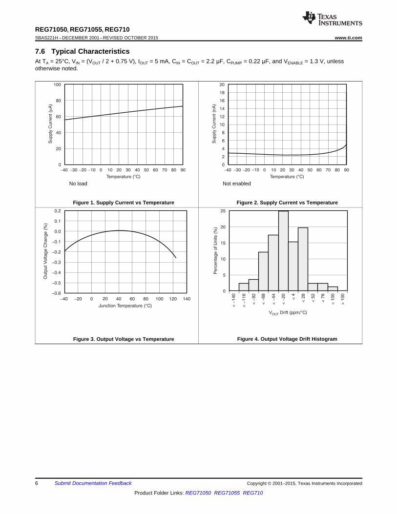
7.6 Typical CharacteristicsAt TA = 25°C, VIN = (VOUT / 2 + 0.75 V), IOUT = 5 mA, CIN = COUT = 2.2 μF, CPUMP = 0.22 μF, and VENABLE = 1.3 V, unlessotherwise noted.
No load Not enabled
Figure 1. Supply Current vs Temperature Figure 2. Supply Current vs Temperature
Figure 4. Output Voltage Drift HistogramFigure 3. Output Voltage vs Temperature
6 Submit Documentation Feedback Copyright © 2001–2015, Texas Instruments Incorporated
Product Folder Links: REG71050 REG71055 REG710
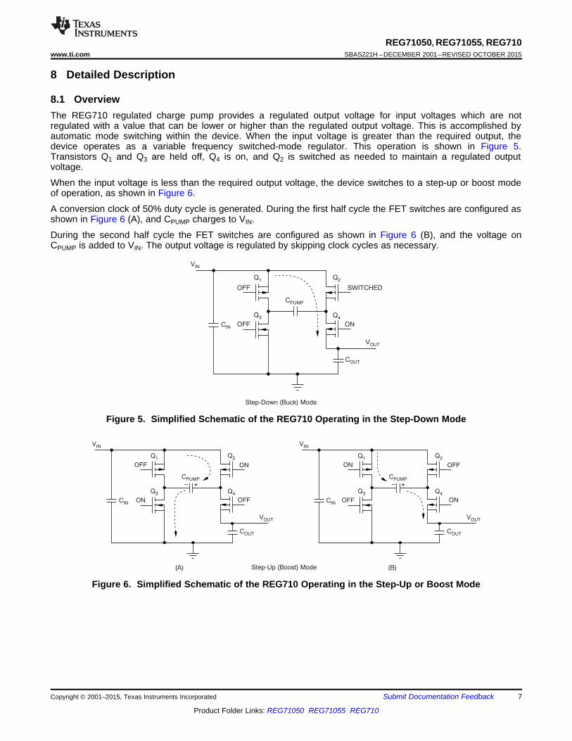
Step-Up (Boost) Mode(A) (B)
OFF
ON
ON
OFF
CPUMP
Q2
Q4
COUT
VOUT
CPUMP
Q2
Q4
COUT
VOUT
OFF
ON
Q1
Q3
ON
OFF
Q1
Q3
CIN
VIN
CIN
VIN
OFF SWITCHED
Step-Down (Buck) Mode
OFF ON
CPUMP
Q1
Q3
Q2
Q4
CIN
COUT
VOUT
VIN
REG71050, REG71055, REG710www.ti.com SBAS221H –DECEMBER 2001–REVISED OCTOBER 2015
8 Detailed Description
8.1 OverviewThe REG710 regulated charge pump provides a regulated output voltage for input voltages which are notregulated with a value that can be lower or higher than the regulated output voltage. This is accomplished byautomatic mode switching within the device. When the input voltage is greater than the required output, thedevice operates as a variable frequency switched-mode regulator. This operation is shown in Figure 5.Transistors Q1 and Q3 are held off, Q4 is on, and Q2 is switched as needed to maintain a regulated outputvoltage.
When the input voltage is less than the required output voltage, the device switches to a step-up or boost modeof operation, as shown in Figure 6.
A conversion clock of 50% duty cycle is generated. During the first half cycle the FET switches are configured asshown in Figure 6 (A), and CPUMP charges to VIN.
During the second half cycle the FET switches are configured as shown in Figure 6 (B), and the voltage onCPUMP is added to VIN. The output voltage is regulated by skipping clock cycles as necessary.
Figure 5. Simplified Schematic of the REG710 Operating in the Step-Down Mode
Figure 6. Simplified Schematic of the REG710 Operating in the Step-Up or Boost Mode
Copyright © 2001–2015, Texas Instruments Incorporated Submit Documentation Feedback 7
Product Folder Links: REG71050 REG71055 REG710

VIN
Enable3
5
4 6
1V
OUT
2 GND
Thermal
Control
&
REG710
CIN
2.2 Fm
COUT
2.2 Fm
CPUMP
0.22 Fm
REG71050, REG71055, REG710SBAS221H –DECEMBER 2001–REVISED OCTOBER 2015 www.ti.com
8.2 Functional Block Diagram
8.3 Feature Description
8.3.1 Shutdown ModeThe EN pin enables the IC when pulled high and places it into energy-saving shutdown mode when pulled low.When in shutdown mode, the output is disconnected from the input and the quiescent current is reduced to 0.01μA typical. This shutdown mode functionality is only valid when VIN is above the minimum recommendedoperating voltage. The EN pin cannot be left floating and must be actively terminated either high or low.
8.3.2 ProtectionThe regulator includes thermal shutdown circuitry protecting the device from damage caused by overloadconditions. The thermal protection circuitry disables the output when the junction temperature reachesapproximately 160°C, allowing the device to cool. When the junction temperature cools to approximately 140°C,the output circuitry is automatically reenabled. Continuously operating the regulator into thermal shutdown candegrade reliability. The regulator also provides current limit to protect itself and the load.
8.4 Device Functional Modes
8.4.1 Peak Current ReductionIn normal operation, the charging of the pump and the output capacitors usually leads to relatively high peakinput currents which can be much higher than the average load current. The regulator incorporates circuitry tolimit the input peak current, lowering the total EMI emission and lowering the output voltage ripple and the inputcurrent ripple. The Input capacitor (CIN) supplies most of the charge required by the input current peaks.
8.4.2 EfficiencyThe efficiency of the charge pump regulator varies with the output voltage version, the applied input voltage, theload current, and the internal operation mode of the device.
The approximate efficiency is given by:
8 Submit Documentation Feedback Copyright © 2001–2015, Texas Instruments Incorporated
Product Folder Links: REG71050 REG71055 REG710
OUT
IN
V100
Vu
OUT INEfficiency (%) = V / (2 V ) 100u u
(step-up operating mode)or
(step-down operating mode)
REG71050, REG71055, REG710www.ti.com SBAS221H –DECEMBER 2001–REVISED OCTOBER 2015
Device Functional Modes (continued)
(1)
Table 1. Operating Mode Change versus VIN
PRODUCT OPERATING MODE CHANGES AT VIN OFREG710-2.5 > 3.2 VREG710-2.7 > 3.4 VREG710-3 > 3.7 V
REG710-3.3 > 4.0 VREG710-5, REG71050, REG71055 Step-up only
Table 1 lists the approximate values of the input voltage at which the device changes internal operating mode.See efficiency curves in Typical Characteristics for various loads and input voltages.
Copyright © 2001–2015, Texas Instruments Incorporated Submit Documentation Feedback 9
Product Folder Links: REG71050 REG71055 REG710

VIN
Enable
VOUT
GND
REG710C
IN
2.2mF
COUT
2.2mF
CPUMP
0.22mF
4 63
5 1
2
REG71050, REG71055, REG710SBAS221H –DECEMBER 2001–REVISED OCTOBER 2015 www.ti.com
9 Application and Implementation
NOTEInformation in the following applications sections is not part of the TI componentspecification, and TI does not warrant its accuracy or completeness. TI’s customers areresponsible for determining suitability of components for their purposes. Customers shouldvalidate and test their design implementation to confirm system functionality.
9.1 Application InformationThe REG710 is a switched capacitor voltage converter that produces a regulated, low-ripple output voltage froman unregulated input voltage range from 1.8 V to 5.5 V. The high switching frequency allows the use of smallsurface-mount capacitors. The following section gives guidance to choose external components to complete thepower supply design. Application curves are included for the typical application shown below.
9.2 Typical Applications
Figure 7. Typical Operating Circuit
9.2.1 Design RequirementsThe REG710 family of switched capacitor voltage converters offers a variety of regulated fixed output voltages.This family supports unregulated input voltages which can have values that are lower or higher than theregulated output voltage. Only input and output capacitors as well as a pump capacitor are required to have afully functional converter. The following design procedure is adequate for the whole VIN, VOUT and load currentrange of REG710.
9.2.2 Detailed Design Procedure
9.2.2.1 Capacitor SelectionFor minimum output voltage ripple, the output capacitor COUT should be a ceramic, surface-mount type. Tantalumcapacitors generally have a higher effective series resistance (ESR) and may contribute to higher output voltageripple. Leaded capacitors also increase ripple due to the higher inductance of the package itself. To achieve bestoperation with low input voltage and high load current, the input and pump capacitors (CIN and CPUMP,respectively) should also be surface-mount ceramic types. In all cases, X7R or X5R dielectric are recommended.See the typical operating circuit shown in Figure 7 for component values.
With light loads or higher input voltage, a smaller 0.1-μF pump capacitor (CPUMP) and smaller 1-μF input andoutput capacitors (CIN and COUT, respectively) can be used. To minimize output voltage ripple, increase theoutput capacitor, COUT, to 10 μF or larger.
The capacitors listed in Table 2 can be used with the REG710. This table is only a representative list ofcompatible parts.
10 Submit Documentation Feedback Copyright © 2001–2015, Texas Instruments Incorporated
Product Folder Links: REG71050 REG71055 REG710

Load Current (mA)
Effic
iency (
%)
90
80
70
60
50
40
301 10 1000.1
V = VIN OUT
VIN = 1.8V
VIN = 2.2V
Load Current (mA)
Effic
iency (
%)
90
80
70
60
50
40
301 10 1000.1
V = VOUTIN
V = 1.8VIN
V = 2.2VIN
V (V)IN
Effic
iency (
%)
90
80
70
60
50
40
302.0 2.5 3.0 3.5 4.0 4.5 5.0 5.51.5
REG710-5, REG71050
REG71055
REG710-3.3
REG710-3
REG710-2.5
REG710-2.7
Load Current (mA)
Effic
iency (
%)
90
80
70
60
50
40
301 10 1000.1
V = VIN OUT
V = 2.7VIN
V = 4.2VIN
V = 3.6VIN
V = 3.3VIN
V = 3VIN
REG71050, REG71055, REG710www.ti.com SBAS221H –DECEMBER 2001–REVISED OCTOBER 2015
Table 2. Suggested CapacitorsRATED
DIELECTRIC PACKAGE WORKINGMANUFACTURER PART NUMBER VALUE TOLERANCE MATERIAL SIZE VOLTAGE
C1206C255K8RAC 2.2 μF ±10% X7R 1206 10 VKemet
C1206C224K8RAC 0.22 μF ±10% X7R 1206 10 VECJ−2YBOJ225K 2.2 μF ±10% X5R 805 6.3 V
Panasonic ECJ−2VBIC224K 0.22 μF ±10% X7R 805 16 VECJ−2VBIC104 0.1 μF ±10% X7R 805 16 V
EMK316BJ225KL 2.2 μF ±10% X7R 1206 16 VTaiyo Yuden
TKM316BJ224KF 0.22 μF ±10% X7R 1206 25 V
9.2.3 Application Curves
REG710-5V,REG71050
Figure 8. Efficiency vs VIN Figure 9. Efficiency vs Load Current
REG710-3.3V REG710-3.3V
Figure 10. Efficiency vs Load Current Figure 11. Efficiency vs Load Current
Copyright © 2001–2015, Texas Instruments Incorporated Submit Documentation Feedback 11
Product Folder Links: REG71050 REG71055 REG710
V (V)IN
Outp
ut R
ipple
(m
V)
PP
90
80
70
60
50
40
30
20
10
01.5 2.0 2.5 3.0 3.5 4.0 4.5 5.0 5.5 6.01.0
REG710-2.7
C = 2.2 FmOUT
REG710-2.7
C = 10 FmOUT
REG710-3.3
C = 2.2 FmOUT
REG710-3.3
C = 10 FmOUT
20mV/div
COUT = 2.2mF
C = 10 F, CmOUT PUMP = 1 Fm
20mV/div
Time (5ms/div)
BW = 20MHz
REG710-3.3V
V = 2.4VIN
RL = 332W
20mV/div VOUT
ILOAD
10mA/div
Time (10 s/div)m
BW = 20MHz
2V/div
3.5V
4.5VVIN
VOUT50mV/div
Time (50 s/div)m
BW = 20MHz
Boost Mode
Buck Mode
REG710-3.3V
R = 1 WL 10
Load Current (mA)
Effic
iency (
%)
80
75
70
65
60
55
50
45
40
35
301 10 1000.1
V = VIN OUT
V = 1.8VIN
V = 2.2VIN
Load Current (mA)
Effic
iency (
%)
80
75
70
65
60
55
50
45
40
35
301 10 1000.1
V = VIN OUT
VIN = 1.8V
V = 2.2VIN
REG71050, REG71055, REG710SBAS221H –DECEMBER 2001–REVISED OCTOBER 2015 www.ti.com
REG710-2.7V REG710-2.5
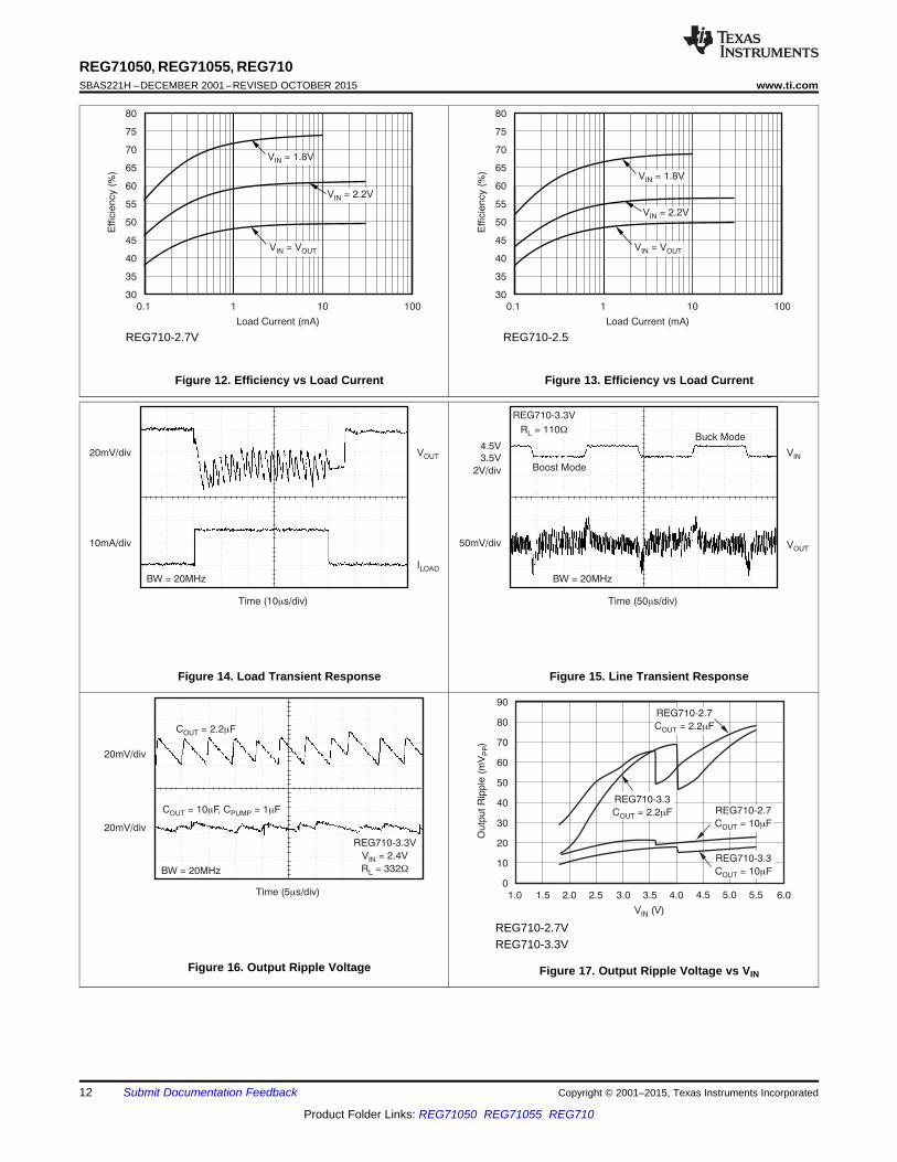
Figure 12. Efficiency vs Load Current Figure 13. Efficiency vs Load Current
Figure 14. Load Transient Response Figure 15. Line Transient Response
REG710-2.7VREG710-3.3V
Figure 16. Output Ripple Voltage Figure 17. Output Ripple Voltage vs VIN
12 Submit Documentation Feedback Copyright © 2001–2015, Texas Instruments Incorporated
Product Folder Links: REG71050 REG71055 REG710
100mA/div IIN
VOUT
2V/div
Time (50 s/div)m
BW = 20MHz
REG710-3.3V
V = 3.0VIN
I = 30mAO
V (V)IN
Outp
ut R
ipple
(m
V)
PP
90
80
70
60
50
40
30
20
10
01.5 2.0 2.5 3.0 3.5 4.0 4.5 5.0 5.5 6.01.0
REG710-3
C = 2.2 FmOUT
REG710-5REG71050
C = 10 FmOUT
REG710-5REG71050
C = 2.2 FmOUT
REG710-3
C = 10 FmOUT
REG710-2.5
C = 2.2 FmOUT
REG710-2.5, C = 10 FmOUT
V (V)IN
Load C
urr
ent (m
A)
250
225
200
175
150
125
100
75
50
25
02.0 2.5 3.0 3.5 4.0 4.5 5.0 5.51.5
REG71050, REG71055, REG710www.ti.com SBAS221H –DECEMBER 2001–REVISED OCTOBER 2015
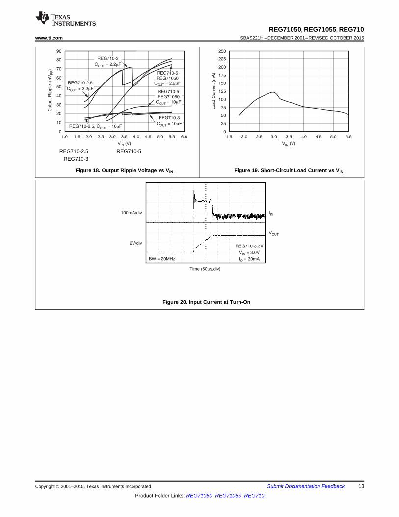
REG710-2.5 REG710-5REG710-3
Figure 18. Output Ripple Voltage vs VIN Figure 19. Short-Circuit Load Current vs VIN
Figure 20. Input Current at Turn-On
Copyright © 2001–2015, Texas Instruments Incorporated Submit Documentation Feedback 13
Product Folder Links: REG71050 REG71055 REG710

2.2 Fm
CIN
VIN
2.2 Fm2.2 Fm
COUT
+
-
0.22 Fm
CP1
REG710-3.3
REG710-3
REG71050
REG710-5
3.3V
3.0V 5.0V
EN GND
VIN
VOUT
0.22 Fm
CP2
EN GND
VIN
VOUT
1.8V
REG71050, REG71055, REG710SBAS221H –DECEMBER 2001–REVISED OCTOBER 2015 www.ti.com
9.3 System Examples
9.3.1 1.8 V to 5.0 V With 10-mA Output CurrentThe REG710 family of charge pumps can be cascaded to reach higher output voltages, as shown in Figure 21.
Figure 21. REG710 Circuit for Step-Up Operation From 1.8 V to 5 V With 10-mA Output Current
This application circuits operates from 1.8 V input voltage and generates 5 V output voltage supporting 10 mAload current.
Higher output voltages can be achieved when two REG710 devices are connected in cascade. When cascadingtwo devices from the REG710 family, the relationship between output current and input voltage must be takeninto account. (see Electrical Characteristics). In this case, REG710 can deliver a maximum of 10 mA. REG710-3.3 or REG710-3 can be used. A second charge pump, REG71050 or REG710-5, steps up the voltage from 3 Vor 3.3 V to 5 V. Connect both Enable pins together.
14 Submit Documentation Feedback Copyright © 2001–2015, Texas Instruments Incorporated
Product Folder Links: REG71050 REG71055 REG710

0.22 Fm
CP1
REG710-3.3
0.22 Fm
CP2
REG710-3.3
4.7 Fm
CIN
VOUT
VIN
VIN
VOUT
GND
VIN
VOUT
GND
4.7 Fm
COUT
+
-
REG71050, REG71055, REG710www.ti.com SBAS221H –DECEMBER 2001–REVISED OCTOBER 2015
System Examples (continued)9.3.2 Doubling the Output Current
Figure 22. REG710 Circuit for Doubling the Output Current
When higher output currents are required, the REG710 family can be paralleled to double the output current.When paralleling two devices the relationship between output current and input voltage must be taken intoaccount (see Electrical Characteristics).
This particular application can deliver 20 mA for an input voltage from 1.8 V to 5.5 V, or 60-mA output for aninput voltage from 2.2 V to 5.5 V. The output voltage is 3.3 V.
Copyright © 2001–2015, Texas Instruments Incorporated Submit Documentation Feedback 15
Product Folder Links: REG71050 REG71055 REG710
LED
LED
I
VVR
5 -
=
CIN
2.2 Fm
CPUMP
0.22 Fm
3.3V to
4.2V COUT
2.2 Fm
R
LEDGND
Enable
REG71050
REG710-5
LED LED
R R
REG71050, REG71055, REG710SBAS221H –DECEMBER 2001–REVISED OCTOBER 2015 www.ti.com
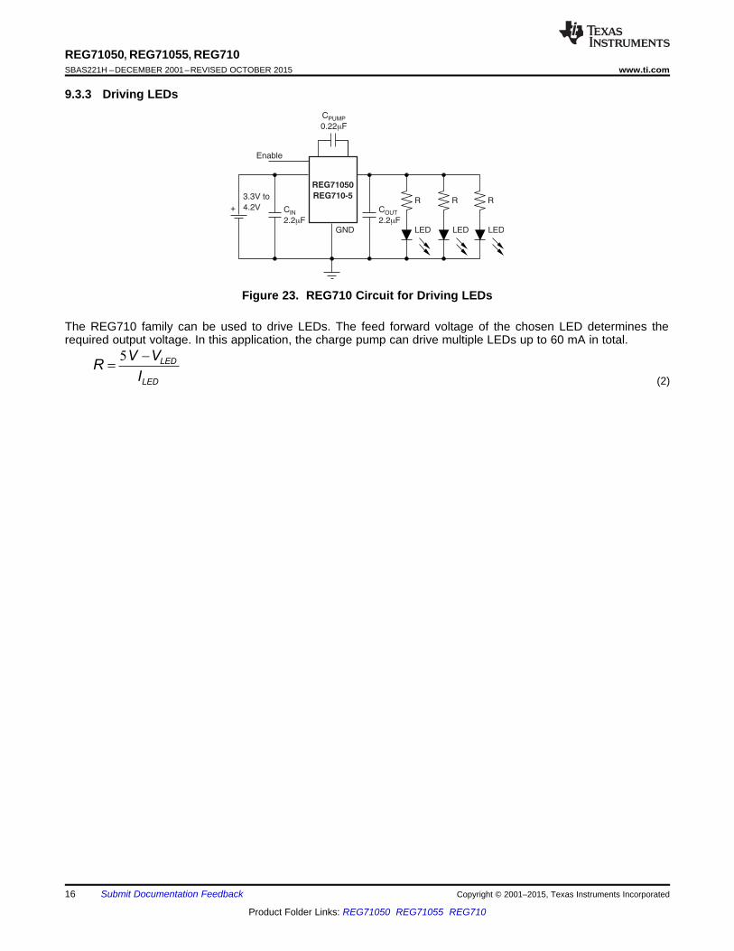
9.3.3 Driving LEDs
Figure 23. REG710 Circuit for Driving LEDs
The REG710 family can be used to drive LEDs. The feed forward voltage of the chosen LED determines therequired output voltage. In this application, the charge pump can drive multiple LEDs up to 60 mA in total.
(2)
16 Submit Documentation Feedback Copyright © 2001–2015, Texas Instruments Incorporated
Product Folder Links: REG71050 REG71055 REG710
1
VENABLEArea: < 0.08 in2
GNDCINCP
COUT
VOUT
VIN
REG71050, REG71055, REG710www.ti.com SBAS221H –DECEMBER 2001–REVISED OCTOBER 2015
10 Power Supply RecommendationsThe input supply to the REG710 must have a current rating according to the supply voltage, output voltage andoutput current of the REG710.
11 Layout
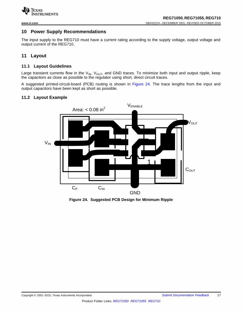
11.1 Layout GuidelinesLarge transient currents flow in the VIN, VOUT, and GND traces. To minimize both input and output ripple, keepthe capacitors as close as possible to the regulator using short, direct circuit traces.
A suggested printed-circuit-board (PCB) routing is shown in Figure 24. The trace lengths from the input andoutput capacitors have been kept as short as possible.
11.2 Layout Example
Figure 24. Suggested PCB Design for Minimum Ripple
Copyright © 2001–2015, Texas Instruments Incorporated Submit Documentation Feedback 17
Product Folder Links: REG71050 REG71055 REG710
REG71050, REG71055, REG710SBAS221H –DECEMBER 2001–REVISED OCTOBER 2015 www.ti.com
12 Device and Documentation Support
12.1 Device Support
12.1.1 Third-Party Products DisclaimerTI'S PUBLICATION OF INFORMATION REGARDING THIRD-PARTY PRODUCTS OR SERVICES DOES NOTCONSTITUTE AN ENDORSEMENT REGARDING THE SUITABILITY OF SUCH PRODUCTS OR SERVICESOR A WARRANTY, REPRESENTATION OR ENDORSEMENT OF SUCH PRODUCTS OR SERVICES, EITHERALONE OR IN COMBINATION WITH ANY TI PRODUCT OR SERVICE.
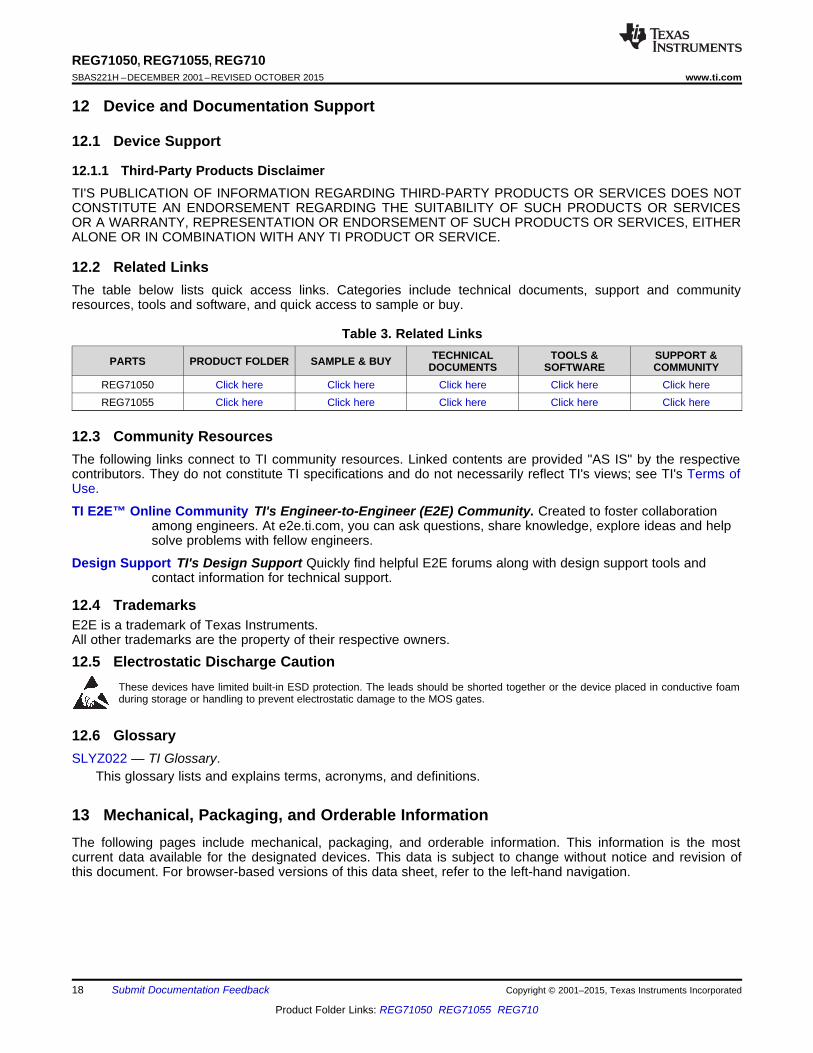
12.2 Related LinksThe table below lists quick access links. Categories include technical documents, support and communityresources, tools and software, and quick access to sample or buy.
Table 3. Related LinksTECHNICAL TOOLS & SUPPORT &PARTS PRODUCT FOLDER SAMPLE & BUY DOCUMENTS SOFTWARE COMMUNITY
REG71050 Click here Click here Click here Click here Click hereREG71055 Click here Click here Click here Click here Click here
12.3 Community ResourcesThe following links connect to TI community resources. Linked contents are provided "AS IS" by the respectivecontributors. They do not constitute TI specifications and do not necessarily reflect TI's views; see TI's Terms ofUse.
TI E2E™ Online Community TI's Engineer-to-Engineer (E2E) Community. Created to foster collaborationamong engineers. At e2e.ti.com, you can ask questions, share knowledge, explore ideas and helpsolve problems with fellow engineers.
Design Support TI's Design Support Quickly find helpful E2E forums along with design support tools andcontact information for technical support.
12.4 TrademarksE2E is a trademark of Texas Instruments.All other trademarks are the property of their respective owners.
12.5 Electrostatic Discharge CautionThese devices have limited built-in ESD protection. The leads should be shorted together or the device placed in conductive foamduring storage or handling to prevent electrostatic damage to the MOS gates.
12.6 GlossarySLYZ022 — TI Glossary.
This glossary lists and explains terms, acronyms, and definitions.
13 Mechanical, Packaging, and Orderable InformationThe following pages include mechanical, packaging, and orderable information. This information is the mostcurrent data available for the designated devices. This data is subject to change without notice and revision ofthis document. For browser-based versions of this data sheet, refer to the left-hand navigation.
18 Submit Documentation Feedback Copyright © 2001–2015, Texas Instruments Incorporated
Product Folder Links: REG71050 REG71055 REG710

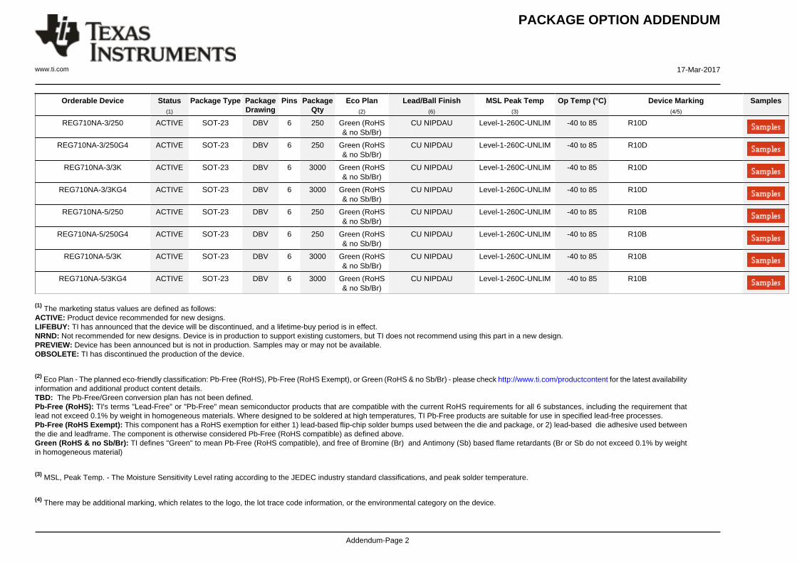
PACKAGE OPTION ADDENDUM
www.ti.com 17-Mar-2017
Addendum-Page 1
PACKAGING INFORMATION
Orderable Device Status(1)
Package Type PackageDrawing
Pins PackageQty
Eco Plan(2)
Lead/Ball Finish(6)
MSL Peak Temp(3)
Op Temp (°C) Device Marking(4/5)
Samples
REG71050DDCR ACTIVE SOT-23-THIN DDC 6 3000 Green (RoHS& no Sb/Br)
CU NIPDAU Level-1-260C-UNLIM -40 to 85 GAAI
REG71050DDCRG4 ACTIVE SOT-23-THIN DDC 6 3000 Green (RoHS& no Sb/Br)
CU NIPDAU Level-1-260C-UNLIM -40 to 85 GAAI
REG71050DDCT ACTIVE SOT-23-THIN DDC 6 250 Green (RoHS& no Sb/Br)
CU NIPDAU Level-1-260C-UNLIM -40 to 85 GAAI
REG71050DDCTG4 ACTIVE SOT-23-THIN DDC 6 250 Green (RoHS& no Sb/Br)
CU NIPDAU Level-1-260C-UNLIM -40 to 85 GAAI
REG71050DRVR ACTIVE WSON DRV 6 3000 Green (RoHS& no Sb/Br)
CU NIPDAU Level-2-260C-1 YEAR -40 to 85 CFF
REG71050DRVRG4 ACTIVE WSON DRV 6 3000 Green (RoHS& no Sb/Br)
CU NIPDAU Level-2-260C-1 YEAR -40 to 85 CFF
REG71050DRVT ACTIVE WSON DRV 6 250 Green (RoHS& no Sb/Br)
CU NIPDAU Level-2-260C-1 YEAR -40 to 85 CFF
REG71055DDCR ACTIVE SOT-23-THIN DDC 6 3000 Green (RoHS& no Sb/Br)
CU NIPDAU Level-1-260C-UNLIM -40 to 85 R10H
REG71055DDCRG4 ACTIVE SOT-23-THIN DDC 6 3000 Green (RoHS& no Sb/Br)
CU NIPDAU Level-1-260C-UNLIM -40 to 85 R10H
REG71055DDCT ACTIVE SOT-23-THIN DDC 6 250 Green (RoHS& no Sb/Br)
CU NIPDAU Level-1-260C-UNLIM -40 to 85 R10H
REG71055DDCTG4 ACTIVE SOT-23-THIN DDC 6 250 Green (RoHS& no Sb/Br)
CU NIPDAU Level-1-260C-UNLIM -40 to 85 R10H
REG710NA-2.5/250 ACTIVE SOT-23 DBV 6 250 Green (RoHS& no Sb/Br)
CU NIPDAU Level-1-260C-UNLIM -40 to 85 R10G
REG710NA-2.5/250G4 ACTIVE SOT-23 DBV 6 250 Green (RoHS& no Sb/Br)
CU NIPDAU Level-1-260C-UNLIM -40 to 85 R10G
REG710NA-2.7/250 ACTIVE SOT-23 DBV 6 250 Green (RoHS& no Sb/Br)
CU NIPDAU Level-1-260C-UNLIM -40 to 85 R10F
REG710NA-3.3/250 ACTIVE SOT-23 DBV 6 250 Green (RoHS& no Sb/Br)
CU NIPDAU Level-1-260C-UNLIM -40 to 85 R10C
REG710NA-3.3/250G4 ACTIVE SOT-23 DBV 6 250 Green (RoHS& no Sb/Br)
CU NIPDAU Level-1-260C-UNLIM -40 to 85 R10C
REG710NA-3.3/3K ACTIVE SOT-23 DBV 6 3000 Green (RoHS& no Sb/Br)
CU NIPDAU Level-1-260C-UNLIM -40 to 85 R10C
PACKAGE OPTION ADDENDUM
www.ti.com 17-Mar-2017
Addendum-Page 2
Orderable Device Status(1)
Package Type PackageDrawing
Pins PackageQty
Eco Plan(2)
Lead/Ball Finish(6)
MSL Peak Temp(3)
Op Temp (°C) Device Marking(4/5)
Samples
REG710NA-3/250 ACTIVE SOT-23 DBV 6 250 Green (RoHS& no Sb/Br)
CU NIPDAU Level-1-260C-UNLIM -40 to 85 R10D
REG710NA-3/250G4 ACTIVE SOT-23 DBV 6 250 Green (RoHS& no Sb/Br)
CU NIPDAU Level-1-260C-UNLIM -40 to 85 R10D
REG710NA-3/3K ACTIVE SOT-23 DBV 6 3000 Green (RoHS& no Sb/Br)
CU NIPDAU Level-1-260C-UNLIM -40 to 85 R10D
REG710NA-3/3KG4 ACTIVE SOT-23 DBV 6 3000 Green (RoHS& no Sb/Br)
CU NIPDAU Level-1-260C-UNLIM -40 to 85 R10D
REG710NA-5/250 ACTIVE SOT-23 DBV 6 250 Green (RoHS& no Sb/Br)
CU NIPDAU Level-1-260C-UNLIM -40 to 85 R10B
REG710NA-5/250G4 ACTIVE SOT-23 DBV 6 250 Green (RoHS& no Sb/Br)
CU NIPDAU Level-1-260C-UNLIM -40 to 85 R10B
REG710NA-5/3K ACTIVE SOT-23 DBV 6 3000 Green (RoHS& no Sb/Br)
CU NIPDAU Level-1-260C-UNLIM -40 to 85 R10B
REG710NA-5/3KG4 ACTIVE SOT-23 DBV 6 3000 Green (RoHS& no Sb/Br)
CU NIPDAU Level-1-260C-UNLIM -40 to 85 R10B
(1) The marketing status values are defined as follows:ACTIVE: Product device recommended for new designs.LIFEBUY: TI has announced that the device will be discontinued, and a lifetime-buy period is in effect.NRND: Not recommended for new designs. Device is in production to support existing customers, but TI does not recommend using this part in a new design.PREVIEW: Device has been announced but is not in production. Samples may or may not be available.OBSOLETE: TI has discontinued the production of the device.
(2) Eco Plan - The planned eco-friendly classification: Pb-Free (RoHS), Pb-Free (RoHS Exempt), or Green (RoHS & no Sb/Br) - please check http://www.ti.com/productcontent for the latest availabilityinformation and additional product content details.TBD: The Pb-Free/Green conversion plan has not been defined.Pb-Free (RoHS): TI's terms "Lead-Free" or "Pb-Free" mean semiconductor products that are compatible with the current RoHS requirements for all 6 substances, including the requirement thatlead not exceed 0.1% by weight in homogeneous materials. Where designed to be soldered at high temperatures, TI Pb-Free products are suitable for use in specified lead-free processes.Pb-Free (RoHS Exempt): This component has a RoHS exemption for either 1) lead-based flip-chip solder bumps used between the die and package, or 2) lead-based die adhesive used betweenthe die and leadframe. The component is otherwise considered Pb-Free (RoHS compatible) as defined above.Green (RoHS & no Sb/Br): TI defines "Green" to mean Pb-Free (RoHS compatible), and free of Bromine (Br) and Antimony (Sb) based flame retardants (Br or Sb do not exceed 0.1% by weightin homogeneous material)
(3) MSL, Peak Temp. - The Moisture Sensitivity Level rating according to the JEDEC industry standard classifications, and peak solder temperature.
(4) There may be additional marking, which relates to the logo, the lot trace code information, or the environmental category on the device.
PACKAGE OPTION ADDENDUM
www.ti.com 17-Mar-2017
Addendum-Page 3
(5) Multiple Device Markings will be inside parentheses. Only one Device Marking contained in parentheses and separated by a "~" will appear on a device. If a line is indented then it is a continuationof the previous line and the two combined represent the entire Device Marking for that device.
(6) Lead/Ball Finish - Orderable Devices may have multiple material finish options. Finish options are separated by a vertical ruled line. Lead/Ball Finish values may wrap to two lines if the finishvalue exceeds the maximum column width.
Important Information and Disclaimer:The information provided on this page represents TI's knowledge and belief as of the date that it is provided. TI bases its knowledge and belief on informationprovided by third parties, and makes no representation or warranty as to the accuracy of such information. Efforts are underway to better integrate information from third parties. TI has taken andcontinues to take reasonable steps to provide representative and accurate information but may not have conducted destructive testing or chemical analysis on incoming materials and chemicals.TI and TI suppliers consider certain information to be proprietary, and thus CAS numbers and other limited information may not be available for release.
In no event shall TI's liability arising out of such information exceed the total purchase price of the TI part(s) at issue in this document sold by TI to Customer on an annual basis.
OTHER QUALIFIED VERSIONS OF REG71055 :
• Automotive: REG71055-Q1
NOTE: Qualified Version Definitions:
• Automotive - Q100 devices qualified for high-reliability automotive applications targeting zero defects
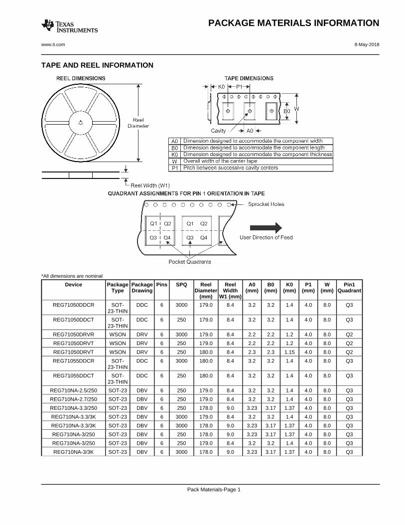
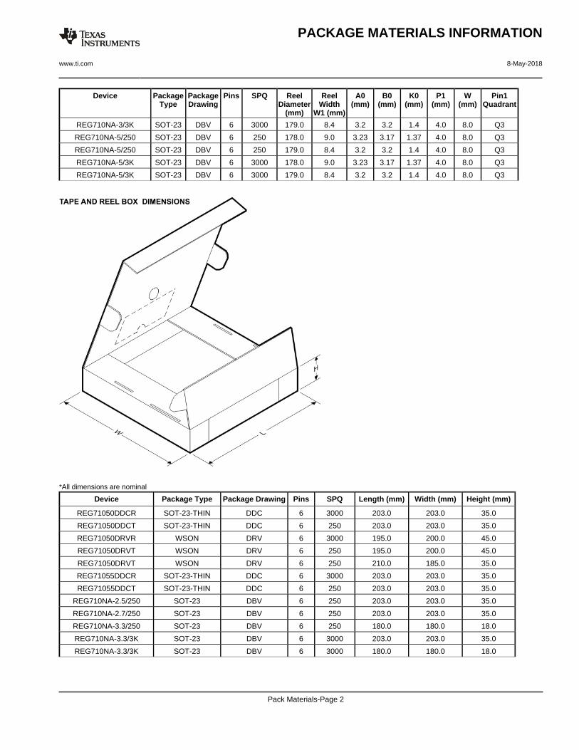
TAPE AND REEL INFORMATION
*All dimensions are nominal
Device PackageType
PackageDrawing
Pins SPQ ReelDiameter
(mm)
ReelWidth
W1 (mm)
A0(mm)
B0(mm)
K0(mm)
P1(mm)
W(mm)
Pin1Quadrant
REG71050DDCR SOT-23-THIN
DDC 6 3000 179.0 8.4 3.2 3.2 1.4 4.0 8.0 Q3
REG71050DDCT SOT-23-THIN
DDC 6 250 179.0 8.4 3.2 3.2 1.4 4.0 8.0 Q3
REG71050DRVR WSON DRV 6 3000 179.0 8.4 2.2 2.2 1.2 4.0 8.0 Q2
REG71050DRVT WSON DRV 6 250 179.0 8.4 2.2 2.2 1.2 4.0 8.0 Q2
REG71050DRVT WSON DRV 6 250 180.0 8.4 2.3 2.3 1.15 4.0 8.0 Q2
REG71055DDCR SOT-23-THIN
DDC 6 3000 180.0 8.4 3.2 3.2 1.4 4.0 8.0 Q3
REG71055DDCT SOT-23-THIN
DDC 6 250 180.0 8.4 3.2 3.2 1.4 4.0 8.0 Q3
REG710NA-2.5/250 SOT-23 DBV 6 250 179.0 8.4 3.2 3.2 1.4 4.0 8.0 Q3
REG710NA-2.7/250 SOT-23 DBV 6 250 179.0 8.4 3.2 3.2 1.4 4.0 8.0 Q3
REG710NA-3.3/250 SOT-23 DBV 6 250 178.0 9.0 3.23 3.17 1.37 4.0 8.0 Q3
REG710NA-3.3/3K SOT-23 DBV 6 3000 179.0 8.4 3.2 3.2 1.4 4.0 8.0 Q3
REG710NA-3.3/3K SOT-23 DBV 6 3000 178.0 9.0 3.23 3.17 1.37 4.0 8.0 Q3
REG710NA-3/250 SOT-23 DBV 6 250 178.0 9.0 3.23 3.17 1.37 4.0 8.0 Q3
REG710NA-3/250 SOT-23 DBV 6 250 179.0 8.4 3.2 3.2 1.4 4.0 8.0 Q3
REG710NA-3/3K SOT-23 DBV 6 3000 178.0 9.0 3.23 3.17 1.37 4.0 8.0 Q3
PACKAGE MATERIALS INFORMATION
www.ti.com 8-May-2018
Pack Materials-Page 1
Device PackageType
PackageDrawing
Pins SPQ ReelDiameter
(mm)
ReelWidth
W1 (mm)
A0(mm)
B0(mm)
K0(mm)
P1(mm)
W(mm)
Pin1Quadrant
REG710NA-3/3K SOT-23 DBV 6 3000 179.0 8.4 3.2 3.2 1.4 4.0 8.0 Q3
REG710NA-5/250 SOT-23 DBV 6 250 178.0 9.0 3.23 3.17 1.37 4.0 8.0 Q3
REG710NA-5/250 SOT-23 DBV 6 250 179.0 8.4 3.2 3.2 1.4 4.0 8.0 Q3
REG710NA-5/3K SOT-23 DBV 6 3000 178.0 9.0 3.23 3.17 1.37 4.0 8.0 Q3
REG710NA-5/3K SOT-23 DBV 6 3000 179.0 8.4 3.2 3.2 1.4 4.0 8.0 Q3
*All dimensions are nominal
Device Package Type Package Drawing Pins SPQ Length (mm) Width (mm) Height (mm)
REG71050DDCR SOT-23-THIN DDC 6 3000 203.0 203.0 35.0
REG71050DDCT SOT-23-THIN DDC 6 250 203.0 203.0 35.0
REG71050DRVR WSON DRV 6 3000 195.0 200.0 45.0
REG71050DRVT WSON DRV 6 250 195.0 200.0 45.0
REG71050DRVT WSON DRV 6 250 210.0 185.0 35.0
REG71055DDCR SOT-23-THIN DDC 6 3000 203.0 203.0 35.0
REG71055DDCT SOT-23-THIN DDC 6 250 203.0 203.0 35.0
REG710NA-2.5/250 SOT-23 DBV 6 250 203.0 203.0 35.0
REG710NA-2.7/250 SOT-23 DBV 6 250 203.0 203.0 35.0
REG710NA-3.3/250 SOT-23 DBV 6 250 180.0 180.0 18.0
REG710NA-3.3/3K SOT-23 DBV 6 3000 203.0 203.0 35.0
REG710NA-3.3/3K SOT-23 DBV 6 3000 180.0 180.0 18.0
PACKAGE MATERIALS INFORMATION
www.ti.com 8-May-2018
Pack Materials-Page 2
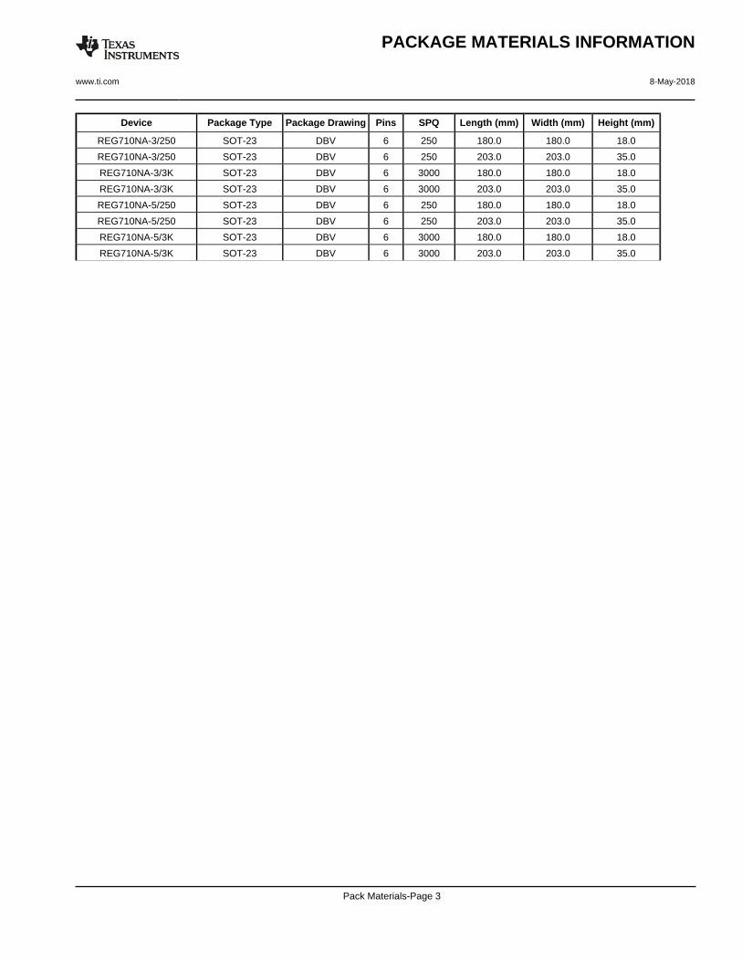
Device Package Type Package Drawing Pins SPQ Length (mm) Width (mm) Height (mm)
REG710NA-3/250 SOT-23 DBV 6 250 180.0 180.0 18.0
REG710NA-3/250 SOT-23 DBV 6 250 203.0 203.0 35.0
REG710NA-3/3K SOT-23 DBV 6 3000 180.0 180.0 18.0
REG710NA-3/3K SOT-23 DBV 6 3000 203.0 203.0 35.0
REG710NA-5/250 SOT-23 DBV 6 250 180.0 180.0 18.0
REG710NA-5/250 SOT-23 DBV 6 250 203.0 203.0 35.0
REG710NA-5/3K SOT-23 DBV 6 3000 180.0 180.0 18.0
REG710NA-5/3K SOT-23 DBV 6 3000 203.0 203.0 35.0
PACKAGE MATERIALS INFORMATION
www.ti.com 8-May-2018
Pack Materials-Page 3

GENERIC PACKAGE VIEW
Images above are just a representation of the package family, actual package may vary.Refer to the product data sheet for package details.
DRV 6 WSON - 0.8 mm max heightPLASTIC SMALL OUTLINE - NO LEAD
4206925/F

www.ti.com
PACKAGE OUTLINE
C
6X 0.350.25
1.6 0.1
6X 0.30.2
2X1.3
1 0.1
4X 0.65
0.80.7
0.050.00
B 2.11.9
A
2.11.9
(0.2) TYP
WSON - 0.8 mm max heightDRV0006APLASTIC SMALL OUTLINE - NO LEAD
4222173/B 04/2018
PIN 1 INDEX AREA
SEATING PLANE
0.08 C
1
34
6
(OPTIONAL)PIN 1 ID
0.1 C A B0.05 C
THERMAL PADEXPOSED
7
NOTES: 1. All linear dimensions are in millimeters. Any dimensions in parenthesis are for reference only. Dimensioning and tolerancing per ASME Y14.5M. 2. This drawing is subject to change without notice. 3. The package thermal pad must be soldered to the printed circuit board for thermal and mechanical performance.
SCALE 5.500
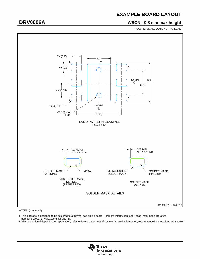
www.ti.com
EXAMPLE BOARD LAYOUT
0.07 MINALL AROUND
0.07 MAXALL AROUND
(1)
4X (0.65)
(1.95)
6X (0.3)
6X (0.45)
(1.6)
(R0.05) TYP
( 0.2) VIATYP
(1.1)
WSON - 0.8 mm max heightDRV0006APLASTIC SMALL OUTLINE - NO LEAD
4222173/B 04/2018
SYMM
1
34
6
SYMM
LAND PATTERN EXAMPLESCALE:25X
7
NOTES: (continued) 4. This package is designed to be soldered to a thermal pad on the board. For more information, see Texas Instruments literature number SLUA271 (www.ti.com/lit/slua271).5. Vias are optional depending on application, refer to device data sheet. If some or all are implemented, recommended via locations are shown.
SOLDER MASKOPENINGSOLDER MASK
METAL UNDER
SOLDER MASKDEFINED
METALSOLDER MASKOPENING
SOLDER MASK DETAILS
NON SOLDER MASKDEFINED
(PREFERRED)

www.ti.com
EXAMPLE STENCIL DESIGN
6X (0.3)
6X (0.45)
4X (0.65)
(0.7)
(1)
(1.95)
(R0.05) TYP
(0.45)
WSON - 0.8 mm max heightDRV0006APLASTIC SMALL OUTLINE - NO LEAD
4222173/B 04/2018
NOTES: (continued) 6. Laser cutting apertures with trapezoidal walls and rounded corners may offer better paste release. IPC-7525 may have alternate design recommendations.
SOLDER PASTE EXAMPLEBASED ON 0.125 mm THICK STENCIL
EXPOSED PAD #7
88% PRINTED SOLDER COVERAGE BY AREA UNDER PACKAGESCALE:30X
SYMM
1
3 4
6
SYMM
METAL7
IMPORTANT NOTICE
Texas Instruments Incorporated (TI) reserves the right to make corrections, enhancements, improvements and other changes to itssemiconductor products and services per JESD46, latest issue, and to discontinue any product or service per JESD48, latest issue. Buyersshould obtain the latest relevant information before placing orders and should verify that such information is current and complete.TI’s published terms of sale for semiconductor products (http://www.ti.com/sc/docs/stdterms.htm) apply to the sale of packaged integratedcircuit products that TI has qualified and released to market. Additional terms may apply to the use or sale of other types of TI products andservices.Reproduction of significant portions of TI information in TI data sheets is permissible only if reproduction is without alteration and isaccompanied by all associated warranties, conditions, limitations, and notices. TI is not responsible or liable for such reproduceddocumentation. Information of third parties may be subject to additional restrictions. Resale of TI products or services with statementsdifferent from or beyond the parameters stated by TI for that product or service voids all express and any implied warranties for theassociated TI product or service and is an unfair and deceptive business practice. TI is not responsible or liable for any such statements.Buyers and others who are developing systems that incorporate TI products (collectively, “Designers”) understand and agree that Designersremain responsible for using their independent analysis, evaluation and judgment in designing their applications and that Designers havefull and exclusive responsibility to assure the safety of Designers' applications and compliance of their applications (and of all TI productsused in or for Designers’ applications) with all applicable regulations, laws and other applicable requirements. Designer represents that, withrespect to their applications, Designer has all the necessary expertise to create and implement safeguards that (1) anticipate dangerousconsequences of failures, (2) monitor failures and their consequences, and (3) lessen the likelihood of failures that might cause harm andtake appropriate actions. Designer agrees that prior to using or distributing any applications that include TI products, Designer willthoroughly test such applications and the functionality of such TI products as used in such applications.TI’s provision of technical, application or other design advice, quality characterization, reliability data or other services or information,including, but not limited to, reference designs and materials relating to evaluation modules, (collectively, “TI Resources”) are intended toassist designers who are developing applications that incorporate TI products; by downloading, accessing or using TI Resources in anyway, Designer (individually or, if Designer is acting on behalf of a company, Designer’s company) agrees to use any particular TI Resourcesolely for this purpose and subject to the terms of this Notice.TI’s provision of TI Resources does not expand or otherwise alter TI’s applicable published warranties or warranty disclaimers for TIproducts, and no additional obligations or liabilities arise from TI providing such TI Resources. TI reserves the right to make corrections,enhancements, improvements and other changes to its TI Resources. TI has not conducted any testing other than that specificallydescribed in the published documentation for a particular TI Resource.Designer is authorized to use, copy and modify any individual TI Resource only in connection with the development of applications thatinclude the TI product(s) identified in such TI Resource. NO OTHER LICENSE, EXPRESS OR IMPLIED, BY ESTOPPEL OR OTHERWISETO ANY OTHER TI INTELLECTUAL PROPERTY RIGHT, AND NO LICENSE TO ANY TECHNOLOGY OR INTELLECTUAL PROPERTYRIGHT OF TI OR ANY THIRD PARTY IS GRANTED HEREIN, including but not limited to any patent right, copyright, mask work right, orother intellectual property right relating to any combination, machine, or process in which TI products or services are used. Informationregarding or referencing third-party products or services does not constitute a license to use such products or services, or a warranty orendorsement thereof. Use of TI Resources may require a license from a third party under the patents or other intellectual property of thethird party, or a license from TI under the patents or other intellectual property of TI.TI RESOURCES ARE PROVIDED “AS IS” AND WITH ALL FAULTS. TI DISCLAIMS ALL OTHER WARRANTIES ORREPRESENTATIONS, EXPRESS OR IMPLIED, REGARDING RESOURCES OR USE THEREOF, INCLUDING BUT NOT LIMITED TOACCURACY OR COMPLETENESS, TITLE, ANY EPIDEMIC FAILURE WARRANTY AND ANY IMPLIED WARRANTIES OFMERCHANTABILITY, FITNESS FOR A PARTICULAR PURPOSE, AND NON-INFRINGEMENT OF ANY THIRD PARTY INTELLECTUALPROPERTY RIGHTS. TI SHALL NOT BE LIABLE FOR AND SHALL NOT DEFEND OR INDEMNIFY DESIGNER AGAINST ANY CLAIM,INCLUDING BUT NOT LIMITED TO ANY INFRINGEMENT CLAIM THAT RELATES TO OR IS BASED ON ANY COMBINATION OFPRODUCTS EVEN IF DESCRIBED IN TI RESOURCES OR OTHERWISE. IN NO EVENT SHALL TI BE LIABLE FOR ANY ACTUAL,DIRECT, SPECIAL, COLLATERAL, INDIRECT, PUNITIVE, INCIDENTAL, CONSEQUENTIAL OR EXEMPLARY DAMAGES INCONNECTION WITH OR ARISING OUT OF TI RESOURCES OR USE THEREOF, AND REGARDLESS OF WHETHER TI HAS BEENADVISED OF THE POSSIBILITY OF SUCH DAMAGES.Unless TI has explicitly designated an individual product as meeting the requirements of a particular industry standard (e.g., ISO/TS 16949and ISO 26262), TI is not responsible for any failure to meet such industry standard requirements.Where TI specifically promotes products as facilitating functional safety or as compliant with industry functional safety standards, suchproducts are intended to help enable customers to design and create their own applications that meet applicable functional safety standardsand requirements. Using products in an application does not by itself establish any safety features in the application. Designers mustensure compliance with safety-related requirements and standards applicable to their applications. Designer may not use any TI products inlife-critical medical equipment unless authorized officers of the parties have executed a special contract specifically governing such use.Life-critical medical equipment is medical equipment where failure of such equipment would cause serious bodily injury or death (e.g., lifesupport, pacemakers, defibrillators, heart pumps, neurostimulators, and implantables). Such equipment includes, without limitation, allmedical devices identified by the U.S. Food and Drug Administration as Class III devices and equivalent classifications outside the U.S.TI may expressly designate certain products as completing a particular qualification (e.g., Q100, Military Grade, or Enhanced Product).Designers agree that it has the necessary expertise to select the product with the appropriate qualification designation for their applicationsand that proper product selection is at Designers’ own risk. Designers are solely responsible for compliance with all legal and regulatoryrequirements in connection with such selection.Designer will fully indemnify TI and its representatives against any damages, costs, losses, and/or liabilities arising out of Designer’s non-compliance with the terms and provisions of this Notice.
Mailing Address: Texas Instruments, Post Office Box 655303, Dallas, Texas 75265Copyright © 2018, Texas Instruments Incorporated