Embed Size (px)
Citation preview

REFERENCE-FREE HIGH-SPEED CMOS PIPELINE
ANALOG-TO-DIGITAL CONVERTERS
MICHAEL FIGUEIREDO
B.Sc. and M.Sc., Universidade Nova de Lisboa, 2007
Submitted in partial fulfillment of the requirements for thedegree of Doctor of Philosophy in Electrical and ComputerEngineering of the Faculdade de Ciencias e Tecnologia ofthe Universidade Nova de Lisboa
Supervisor: Professor Joao Carlos da Palma GoesCo-Supervisor: Professor Guiomar Gaspar de Andrade Evans
March 2012


c© 2012 by Michael Figueiredo, FCT/UNL and UNL.
A Faculdade de Ciencias e Tecnologia e a Universidade Nova
de Lisboa tem o direito, perpetuo e sem limites geograficos,
de arquivar e publicar esta dissertacao atraves de exemplares
impressos reproduzidos em papel ou de forma digital, ou por
qualquer outro meio conhecido ou que venha a ser inventado,
e de a divulgar atraves de repositorios cientıficos e de admitir
a sua copia e distribuicao com objectivos educacionais ou de
investigacao, nao comerciais, desde que seja dado credito ao
autor e editor.


To Sofia and my family.


Acknowledgments
Before the acknowledgements, I would like to state that the order in which everyone
appears has nothing to do with their importance.
I would like to start by thanking Prof. Joao Goes for everything. He was my mentor,
my supervisor, and most importantly my friend, always present throughout my Ph.D.
experience. Prof. Guiomar Evans for her guidance, fun and optimistic attitude, and her
help in all the work developed in this thesis.
Prof. Rui Tavares for all the optimizations carried out for the amplifiers. Prof. Nuno
Paulino for many discussions on MDAC and voltage reference circuits, and assistance in the
many papers we published together. Prof. Luis Oliveira for many discussions on diverse
topics, and the assistance provided in the paper we co-authored together. Prof. Joao Pedro
Oliveira for discussions on parametric amplification, for his help with the verifications of
the padring, and the ordering of PCB components and lab material. Prof. M. Medeiros
Silva for many corrections, suggestions, and commentaries made to our papers, which
naturally improved their quality. Prof. A. Steiger-Garcao for all his help on the paper we
co-authored together, and many useful and insightful discussions on circuit analysis.
Prof. F. Baruqui and Prof. A. Petraglia for their help on the MBTA and MDAC
papers. Particularly, A. Petraglia for being an excellent host when we were on our coop-
eration trip in Rio de Janeiro, Brazil.
I would like to thank all my colleagues and friends at the research lab: Edinei Santin,
Joao Ferreira, B lazej Nowacki, Somayeh Abdollahvand, Joao Pacheco, Joao de Melo, Ivan
Bastos, Carlos Carvalho, Joao Casaleiro, Jose Rui Custodio for many interesting discus-
sions on our work and other off-topic debates about our different cultures. I must especially
emphasize the help of two of them: Edinei Santin for many interesting and sometimes com-
plicated discussions, for all his help on the analysis of the MDACs, the design and layout
of the ADC, and for developing a extremely helpful tool for symbolic analysis of analog
vii

circuits (MSAAC), and Joao Ferreira for his help on the design of the PCB and during
the testing phase of the amplifier.
Colleagues and friends at the telecommunications research lab: Miguel Pereira, Miguel
Luıs, and Francisco Ganhao for all our interesting lunches together.
Designers at S3 Group for guidelines and guidance during the layout phase of the ADC
and ESD protection for the amplifier.
Tomasz Michalak for designing the phase generator for the ADC, and contributing to
the paper we co-authored together. Pawe l Pankiewicz for his masters thesis work, which
extended the proposed 1.5-bit flash quantizer to higher resolutions. Marta Kordasz for
developing a helpful small-signal analysis tool based on Y-Parameters.
Mr. Faustino for all the wirebonding work of all the ADC and amplifier chips. Mr.
Guerreiro for providing some material during the soldering phase of the PCBs.
Portuguese Foundation for Science and Technology for awarding me the grant (BD/
41524/2007) that made all this work possible. I would also like to thank the Department of
Electrical Engineering of the Faculdade de Ciencias e Tecnologia of the Universidade Nova
de Lisboa and CTS-UNINOVA, which, through projects IMPACT (PTDC/EEAELC/
101421/2008), OBiS FRET (PTDC/CTM/099511/2008), and FCT/CAPES (227/09), fi-
nanced the trips to all conferences, workshops, and cooperations, where some of the work
developed in this thesis was presented.
Naturally, I thank my parents and my brother, the rest of my family and Sofia’s parents
for always being around.
I conclude by thanking Sofia (and our best friend, Somi), who was always present for
the good and bad moments, specially for putting up with me during the difficult ones, and
for ultimately sharing my entire Ph.D. experience.
viii

Abstract
More and more signal processing is being transferred to the digital domain to profit from
the technological enhancement of digital circuits. Where technology scaling enhances the
capabilities of digital circuits, it degrades the performance of analog circuits. However,
it is important to note that the impact that technology scaling has on digital circuits is
becoming smaller and smaller, which means that, in nanotechnologies, to enhance energy
and area efficiency, we can not simply depend on the benefits of this scaling. Although, a
share of the efficiency can be obtained from the technology, new circuit architectures and
techniques have to be developed to really push the limits of efficiency.
In data converters, more specifically analog-to-digital converters (ADCs), a decision
can be made: research energy and area efficient analog circuit techniques and architectures
that cope with technological scaling issues, or design algorithms that use digital circuitry
to assist the poor analog technological performance. The former option is the premise for
the work developed in this thesis.
The work reported in this thesis explores various design techniques with the purpose of
enhancing the power and area efficiency of building blocks mainly to be used in multiplying
digital-to-analog converter based ADCs. Therefore, novel analog techniques are developed
for the three main blocks of an MDAC-based stage, namely, the flash quantizer, the
amplifier, and the switched capacitor network of the MDAC. These techniques include
self-biasing and inverter-based design for the flash quantizer and amplifier. Regarding
the MDAC, it combines three techniques: unity feedback factor, insensitivity to capacitor
mismatch, and current-mode reference shifting.
In the second part of this work, the designed amplifier is implemented and experimen-
tally characterized demonstrating its practical feasibility and performance.
The final part of this work explores the design and implementation of a medium-low
resolution high speed pipeline ADC incorporating all the developed circuits. Experimental
ix

results validate the feasibility of the techniques and demonstrate the attractiveness in terms
of power dissipation and reduced area.
Keywords: ADC, amplifier, current-mode, feedback factor, flash quantizer, inverter-
based, MDAC, pipeline, reference buffer, reference voltage, self-biasing, switched-capacitor.
x

Sumario
O escalonamento da tecnologia melhora as capacidades de circuitos digitais, mas degrada
o desempenho de circuitos analogicos. A transferencia de processamento de sinais para
o domınio digital e cada vez maior para tirar proveito destes avancos tecnologicos nos
circuitos digitais. No entanto, e importante notar que o impacto que o escalonamento da
tecnologia esta a ter nos circuitos digitais e cada vez menor, o que significa que, em nanotec-
nologias, para melhorar a eficiencia energetica e a area dos circuitos, nao se pode depender
apenas dos benefıcios da tecnologia. Embora, uma parte significativa da eficiencia pode
ser obtida a partir da tecnologia, novas tecnicas e arquitecturas de circuitos tem de ser
desenvolvidas para conseguir atingir e ultrapassar os actuais limites de eficiencia.
Em conversores de dados, mais especificamente conversores analogico-digital (ADCs),
uma decisao importante deve ser tomada: pesquisar tecnicas e arquitecturas de circuitos
analogicos que melhoram a eficiencia energetica e de area, e que lidam com as questoes de
escalonamento tecnologico ou implementar algoritmos que aproveitam os circuitos digitais
para mitigar o mau desempenho dos circuitos analogicos. A primeira opcao e a escolhida
para o trabalho desenvolvido nesta tese.
O trabalho apresentado nesta tese explora varias tecnicas com o objetivo de aumentar
a eficiencia de energia e de area de blocos a ser usados em ADCs baseados em conversores
digital-analogico multiplicativos (MDACs). Assim, novas tecnicas analogicas sao desen-
volvidas para os tres blocos principais de um andar baseado em MDAC: o quantizador
paralelo, o amplificador e o circuito de condensadores comutados do MDAC. Estas tecnicas
incluem auto-polarizacao e a utilizacao de inversores no quantizador paralelo e no amplifi-
cador. Em relacao ao MDAC, este possui um factor de realimentacao unitario, e insensıvel
aos erros de emparelhamento das capacidades, e a soma/subtraccao das referencias e feita
em corrente.
A segunda parte deste trabalho consiste na implementacao do amplificador e na sua
xi

caracterizacao experimental. E tambem demonstrado o seu desempenho e viabilidade
pratica.
A parte final deste trabalho explora a implementacao de um conversor concorrencial de
media-baixa resolucao e de alta velocidade, incorporando todos os circuitos desenvolvidos
acima mencionados. Resultados experimentais validam e demonstram a viabilidade destas
tecnicas em termos de dissipacao de potencia e area reduzida.
Palavras-Chave: amplificador, auto-polarizacao, buffer de referencias, concorren-
cial, condensadores comutados, conversor analogico-digital, conversor digital-analogico
multiplicativo, factor de realimentacao, inversores, quantizador paralelo, referencias em
corrente, tensao de referencia.
xii

Table of Contents
Table of Contents . . . . . . . . . . . . . . . . . . . . . . . . . . . . . . . . . . xiii
List of Figures . . . . . . . . . . . . . . . . . . . . . . . . . . . . . . . . . . . . xvii
List of Tables . . . . . . . . . . . . . . . . . . . . . . . . . . . . . . . . . . . . xxi
Chapter 1 Introduction . . . . . . . . . . . . . . . . . . . . . . . . . . . . . 1
1.1 Motivation . . . . . . . . . . . . . . . . . . . . . . . . . . . . . . . . . . . . 1
1.2 Original Contributions . . . . . . . . . . . . . . . . . . . . . . . . . . . . . . 3
1.3 Thesis Organization . . . . . . . . . . . . . . . . . . . . . . . . . . . . . . . 4
Chapter 2 General Overview of Pipeline Analog-to-Digital Converters 7
2.1 Overview . . . . . . . . . . . . . . . . . . . . . . . . . . . . . . . . . . . . . 7
2.2 MDAC-based Analog-to-Digital Converter Architectures . . . . . . . . . . . 8
2.2.1 Two-Step Flash ADC . . . . . . . . . . . . . . . . . . . . . . . . . . 8
2.2.2 Pipeline ADC . . . . . . . . . . . . . . . . . . . . . . . . . . . . . . . 10
2.2.3 Multi-Step Algorithmic ADC . . . . . . . . . . . . . . . . . . . . . . 12
2.2.4 Time-Interleaving ADCs . . . . . . . . . . . . . . . . . . . . . . . . . 13
2.3 Building Blocks of Pipeline Analog-to-Digital Converters . . . . . . . . . . . 16
2.3.1 Sample-and-Hold . . . . . . . . . . . . . . . . . . . . . . . . . . . . . 16
2.3.2 Multiplying-DAC . . . . . . . . . . . . . . . . . . . . . . . . . . . . . 17
2.3.3 Local Flash Quantizer and Comparators . . . . . . . . . . . . . . . . 20
2.3.4 Operational Amplifier and Common-Mode Feedback Circuitry . . . 22
2.3.5 Reference V/I and Buffering . . . . . . . . . . . . . . . . . . . . . . 27
2.3.6 Clock Generation . . . . . . . . . . . . . . . . . . . . . . . . . . . . . 32
2.3.7 Digital Backend and Decimation . . . . . . . . . . . . . . . . . . . . 34
2.4 Performance Metrics of Analog-to-Digital Converters . . . . . . . . . . . . . 37
2.4.1 Static Performance Parameters . . . . . . . . . . . . . . . . . . . . . 37
2.4.2 Dynamic Performance Parameters . . . . . . . . . . . . . . . . . . . 41
2.5 Overview and Comparison of Published Work . . . . . . . . . . . . . . . . . 44
2.5.1 Two-stage Opamps . . . . . . . . . . . . . . . . . . . . . . . . . . . . 44
2.5.2 Medium-Low Resolution High-Speed MDAC-based ADCs . . . . . . 46
2.5.3 ADC Reference Voltage Circuitry . . . . . . . . . . . . . . . . . . . . 48
Chapter 3 Capacitor Mismatch-Insensitive Multiplying-DAC Topolo-gies with Unity Feedback Factor . . . . . . . . . . . . . . . . . . . . . . . 53
3.1 Overview . . . . . . . . . . . . . . . . . . . . . . . . . . . . . . . . . . . . . 53
3.2 Conventional MDAC . . . . . . . . . . . . . . . . . . . . . . . . . . . . . . . 53
3.2.1 Principle of Operation . . . . . . . . . . . . . . . . . . . . . . . . . . 53
3.2.2 Gain and Reference Shifting Error Analysis . . . . . . . . . . . . . . 54
3.2.3 Feedback Factor . . . . . . . . . . . . . . . . . . . . . . . . . . . . . 56
xiii

3.2.4 Thermal Noise Analysis . . . . . . . . . . . . . . . . . . . . . . . . . 573.3 Current-Mode Reference Shifting MDAC . . . . . . . . . . . . . . . . . . . . 59
3.3.1 Principle of Operation . . . . . . . . . . . . . . . . . . . . . . . . . . 593.3.2 Gain Error Analysis . . . . . . . . . . . . . . . . . . . . . . . . . . . 603.3.3 Reference Shifting Error Analysis . . . . . . . . . . . . . . . . . . . . 663.3.4 Feedback Factor . . . . . . . . . . . . . . . . . . . . . . . . . . . . . 703.3.5 Thermal Noise Analysis . . . . . . . . . . . . . . . . . . . . . . . . . 71
3.4 Sampling Phase Reference Shifting MDAC . . . . . . . . . . . . . . . . . . . 733.4.1 Principle of Operation . . . . . . . . . . . . . . . . . . . . . . . . . . 733.4.2 Gain Error Analysis . . . . . . . . . . . . . . . . . . . . . . . . . . . 753.4.3 Reference Shifting Error Analysis . . . . . . . . . . . . . . . . . . . . 763.4.4 Feedback Factor . . . . . . . . . . . . . . . . . . . . . . . . . . . . . 773.4.5 Thermal Noise Analysis . . . . . . . . . . . . . . . . . . . . . . . . . 77
3.5 Performance Summary and Comparison of 1.5-bit MDACs . . . . . . . . . . 78
Chapter 4 Application of Circuit Enhancement Techniques to ADCBuilding Blocks . . . . . . . . . . . . . . . . . . . . . . . . . . . . . . . . . 814.1 Overview . . . . . . . . . . . . . . . . . . . . . . . . . . . . . . . . . . . . . 814.2 Inverter-Based Self-Biased 1.5-bit Flash Quantizer . . . . . . . . . . . . . . 82
4.2.1 Principle of Operation . . . . . . . . . . . . . . . . . . . . . . . . . . 834.2.2 Circuit and Performance Analysis . . . . . . . . . . . . . . . . . . . 864.2.3 Design Procedure . . . . . . . . . . . . . . . . . . . . . . . . . . . . . 984.2.4 Performance Summary and Comparison . . . . . . . . . . . . . . . . 100
4.3 Two-Stage Inverter-Based Self-Biased Opamp . . . . . . . . . . . . . . . . . 1034.3.1 Principle of Operation . . . . . . . . . . . . . . . . . . . . . . . . . . 1044.3.2 Circuit Analysis . . . . . . . . . . . . . . . . . . . . . . . . . . . . . 1074.3.3 Design Procedure and Optimization . . . . . . . . . . . . . . . . . . 126
Chapter 5 Design of a 7-bit 1 GS/s CMOS Two-Way Interleaved PipelineADC . . . . . . . . . . . . . . . . . . . . . . . . . . . . . . . . . . . . . . . . 1315.1 Overview . . . . . . . . . . . . . . . . . . . . . . . . . . . . . . . . . . . . . 1315.2 Specifications . . . . . . . . . . . . . . . . . . . . . . . . . . . . . . . . . . . 1315.3 Architecture . . . . . . . . . . . . . . . . . . . . . . . . . . . . . . . . . . . . 1325.4 Implementation Details . . . . . . . . . . . . . . . . . . . . . . . . . . . . . 133
5.4.1 Sample-and-Hold . . . . . . . . . . . . . . . . . . . . . . . . . . . . . 1335.4.2 CMRS Multiplying-DAC . . . . . . . . . . . . . . . . . . . . . . . . 1355.4.3 Flash Quantizer . . . . . . . . . . . . . . . . . . . . . . . . . . . . . 1395.4.4 Opamp and CMFB . . . . . . . . . . . . . . . . . . . . . . . . . . . . 1425.4.5 Switches and Clock-Bootstrapping Circuits . . . . . . . . . . . . . . 1445.4.6 Clock Generator . . . . . . . . . . . . . . . . . . . . . . . . . . . . . 1475.4.7 Common-Mode Voltage Buffer . . . . . . . . . . . . . . . . . . . . . 1475.4.8 Digital Backend . . . . . . . . . . . . . . . . . . . . . . . . . . . . . 1485.4.9 Decimator . . . . . . . . . . . . . . . . . . . . . . . . . . . . . . . . . 1505.4.10 Complete ADC . . . . . . . . . . . . . . . . . . . . . . . . . . . . . . 152
Chapter 6 Integrated Prototypes and Experimental Results . . . . . . . 1556.1 Overview . . . . . . . . . . . . . . . . . . . . . . . . . . . . . . . . . . . . . 1556.2 Two-Stage Inverter-Based Self-Biased Amplifier . . . . . . . . . . . . . . . . 155
6.2.1 Floorplan and Layout . . . . . . . . . . . . . . . . . . . . . . . . . . 1566.2.2 Design Considerations . . . . . . . . . . . . . . . . . . . . . . . . . . 1576.2.3 PCB and Test Setup . . . . . . . . . . . . . . . . . . . . . . . . . . . 1586.2.4 Experimental Results . . . . . . . . . . . . . . . . . . . . . . . . . . 160
xiv

6.3 7-bit 1 GS/s CMOS Two-Way Interleaved Pipeline ADC . . . . . . . . . . . 1646.3.1 Floorplan and Layout . . . . . . . . . . . . . . . . . . . . . . . . . . 1646.3.2 Layout Considerations . . . . . . . . . . . . . . . . . . . . . . . . . . 1676.3.3 PCB and Test Setup . . . . . . . . . . . . . . . . . . . . . . . . . . . 1686.3.4 Employed Methodology for Tuning the Reference Currents . . . . . 1706.3.5 Experimental Results . . . . . . . . . . . . . . . . . . . . . . . . . . 172
Chapter 7 Conclusions . . . . . . . . . . . . . . . . . . . . . . . . . . . . . . 1797.1 Summary and Conclusions . . . . . . . . . . . . . . . . . . . . . . . . . . . . 1797.2 Future Work . . . . . . . . . . . . . . . . . . . . . . . . . . . . . . . . . . . 181
Bibliography . . . . . . . . . . . . . . . . . . . . . . . . . . . . . . . . . . . . . 183
xv

xvi

List of Figures
2.1 The Two-Step A/D converter. . . . . . . . . . . . . . . . . . . . . . . . . . . . . . . 92.2 The Pipeline A/D converter. . . . . . . . . . . . . . . . . . . . . . . . . . . . . . . 112.3 The Algorithmic A/D converter. . . . . . . . . . . . . . . . . . . . . . . . . . . . . 132.4 Time-interleaving of A/D converters. . . . . . . . . . . . . . . . . . . . . . . . . . . 142.5 Simple versions of a S/H and a T/H. . . . . . . . . . . . . . . . . . . . . . . . . . . 172.6 Block diagram of a generic N -bit MDAC. . . . . . . . . . . . . . . . . . . . . . . . 182.7 Closed-loop switched-capacitor opamp-based 1.5-bit MDAC. . . . . . . . . . . . . . 182.8 Input-Output characteristics of the 1.5-bit MDAC and the effects of errors. . . . . 192.9 Flash quantizer examples. . . . . . . . . . . . . . . . . . . . . . . . . . . . . . . . . 212.10 Opamp. . . . . . . . . . . . . . . . . . . . . . . . . . . . . . . . . . . . . . . . . . . 232.11 Example using an opamp in a feedback loop. . . . . . . . . . . . . . . . . . . . . . 242.12 Time-domain opamp output response. . . . . . . . . . . . . . . . . . . . . . . . . . 262.13 Simple two-phase nonoverlapping clock generator and output waveforms. . . . . . . 332.14 Simple example of synchronization. . . . . . . . . . . . . . . . . . . . . . . . . . . . 352.15 Example of the operation of digital correction. . . . . . . . . . . . . . . . . . . . . 362.16 Ideal 3-bit A/D converter. . . . . . . . . . . . . . . . . . . . . . . . . . . . . . . . . 382.17 Offset and gain errors. . . . . . . . . . . . . . . . . . . . . . . . . . . . . . . . . . . 392.18 Differential and integral nonlinearity. . . . . . . . . . . . . . . . . . . . . . . . . . . 402.19 Example of an FFT of a two-channel time-interleaved ADC. . . . . . . . . . . . . . 422.20 Two-stage opamp state-of-the-art. . . . . . . . . . . . . . . . . . . . . . . . . . . . 452.21 ADC state-of-the-art. . . . . . . . . . . . . . . . . . . . . . . . . . . . . . . . . . . 482.22 Overview of the ADC reference voltage circuitry data set’s characteristics. . . . . . 492.23 Reference circuit relationships. . . . . . . . . . . . . . . . . . . . . . . . . . . . . . 51
3.1 Conventional fully differential 1.5-bit MDAC. . . . . . . . . . . . . . . . . . . . . . 543.2 Conventional single-ended 1.5-bit MDAC with parasitic capacitors. . . . . . . . . . 553.3 Standard deviation of GE and RE over capacitor mismatch, σ(εij). . . . . . . . . . 563.4 Equivalent circuit for thermal noise analysis of the conventional MDAC. . . . . . . 573.5 Enhanced feedback factor mismatch-insensitive MDAC with current-mode RS. . . 603.6 Equivalent circuit to demonstrate the current-mode reference shifting. . . . . . . . 603.7 Compensation circuit close-up and parasitic capacitor analysis. . . . . . . . . . . . 623.8 Gain error analysis. . . . . . . . . . . . . . . . . . . . . . . . . . . . . . . . . . . . . 633.9 Iso-accuracy lines for the GE vs α vs parasitic capacitor mismatch. . . . . . . . . . 643.10 Comparison between the conventional and the CMRS-MDAC for different A0. . . . 643.11 Output offset due to charge injection, clock feed-through, and VCM mismatch. . . 663.12 MDAC configuration with current-mode reference shifting active. . . . . . . . . . . 673.13 Iso-VREF lines vs GBW vs IREF . . . . . . . . . . . . . . . . . . . . . . . . . . . . . 693.14 Step response comparison between conventional MDAC and CMRS-MDAC. . . . . 703.15 Equivalent circuits for thermal noise analysis of the CMRS-MDAC. . . . . . . . . . 713.16 Enhanced feedback factor mismatch-insensitive MDAC with sampling phase RS. . 743.17 Differential output offset due to VREF charge injection and clock feed-through mis-
match. . . . . . . . . . . . . . . . . . . . . . . . . . . . . . . . . . . . . . . . . . . . 773.18 Equivalent circuits for thermal noise analysis of the SPRS-MDAC. . . . . . . . . . 78
4.1 Proposed 1.5-bit flash quantizer. . . . . . . . . . . . . . . . . . . . . . . . . . . . . 834.2 Input-output waveforms. . . . . . . . . . . . . . . . . . . . . . . . . . . . . . . . . . 85
xvii

4.3 ID − VGS and log(ID)− VGS curves. . . . . . . . . . . . . . . . . . . . . . . . . . . 874.4 Theoretical curve of the quantizer’s threshold voltage, VTH . . . . . . . . . . . . . . 884.5 Kickback noise analysis. . . . . . . . . . . . . . . . . . . . . . . . . . . . . . . . . . 894.6 Regeneration time of the output. . . . . . . . . . . . . . . . . . . . . . . . . . . . . 914.7 Equivalent circuit for metastability analysis. . . . . . . . . . . . . . . . . . . . . . . 924.8 Histograms for 500 Monte Carlo simulations considering PVT corners and mismatch. 964.9 Threshold voltage deviation with respect to PVT corners. . . . . . . . . . . . . . . 974.10 Threshold voltage deviation with respect to VCM variations. . . . . . . . . . . . . . 984.11 Proof-of-functionality. . . . . . . . . . . . . . . . . . . . . . . . . . . . . . . . . . . 994.12 Proposed two-stage inverter-based self-biased amplifier. . . . . . . . . . . . . . . . 1044.13 Common-mode feedback circuits. . . . . . . . . . . . . . . . . . . . . . . . . . . . . 1054.14 Small-signal differential-mode half-circuit of the amplifier. . . . . . . . . . . . . . . 1064.15 Behavioural signal path model of the differential-mode half-circuit. . . . . . . . . . 1084.16 DM pole-zero position diagrams. . . . . . . . . . . . . . . . . . . . . . . . . . . . . 1104.17 Phase margin and nondominant pole damping factor (ζ) variation with CC . . . . . 1114.18 Small-signal common-mode feedback equivalent circuit of the amplifier. . . . . . . 1124.19 CM pole-zero position diagrams. . . . . . . . . . . . . . . . . . . . . . . . . . . . . 1144.20 Differential-mode half-circuit equivalent for noise analysis. . . . . . . . . . . . . . . 1154.21 Differential-mode equivalent for input-referred offset analysis. . . . . . . . . . . . . 1184.22 Differential-mode half-circuit equivalents for slew rate analysis. . . . . . . . . . . . 1194.23 CMFB1’s participation in increasing the total SR. . . . . . . . . . . . . . . . . . . 1214.24 Input stage for input CM range analysis. . . . . . . . . . . . . . . . . . . . . . . . . 1214.25 Input stage transconductance variation over the CMR. . . . . . . . . . . . . . . . . 1234.26 Output stage for output swing analysis. . . . . . . . . . . . . . . . . . . . . . . . . 124
5.1 Block diagram of the selected architecture for the two-way interleaved pipeline ADC.1325.2 Flip-around front-end sample-and-hold circuit. . . . . . . . . . . . . . . . . . . . . 1335.3 Sample-and-hold amplifier. . . . . . . . . . . . . . . . . . . . . . . . . . . . . . . . 1345.4 Sample-and-hold amplifier Bode diagrams. . . . . . . . . . . . . . . . . . . . . . . . 1355.5 1.5-bit time-interleaved stage illustrating shared blocks (shown in grey). . . . . . . 1365.6 Unity feedback factor CMRS-MDAC. . . . . . . . . . . . . . . . . . . . . . . . . . . 1375.7 Reference shifting biasing circuit, including current mirrors and current sources. . . 1385.8 Implemented 1.5-bit flash quantizer. . . . . . . . . . . . . . . . . . . . . . . . . . . 1405.9 Implemented comparator used for VTH = 0 V. . . . . . . . . . . . . . . . . . . . . . 1425.10 MDAC amplifier Bode diagrams. . . . . . . . . . . . . . . . . . . . . . . . . . . . . 1445.11 Implemented clock-bootstrapping scheme. . . . . . . . . . . . . . . . . . . . . . . . 1455.12 Clock-bootstrapping circuit. . . . . . . . . . . . . . . . . . . . . . . . . . . . . . . . 1455.13 Simulated timing diagrams of the clock-bootstrapping circuits. . . . . . . . . . . . 1465.14 Nonoverlapping clock generator: (a) Circuit diagram. (b) Simulated timing diagram. 1475.15 Circuit diagram of the amplifier used to buffer VCM . . . . . . . . . . . . . . . . . . 1485.16 Digital backend. . . . . . . . . . . . . . . . . . . . . . . . . . . . . . . . . . . . . . 1505.17 Block diagram of the time-interleaved decimator. . . . . . . . . . . . . . . . . . . . 1515.18 Circuit diagrams of the 4-bit counter and FFs used in the decimator. . . . . . . . . 1515.19 4096-point FFT of the electrically simulated 7-bit 1 GS/s pipeline ADC for a 20 MHz
input. . . . . . . . . . . . . . . . . . . . . . . . . . . . . . . . . . . . . . . . . . . . 153
6.1 Implementation of the two-stage inverter-based self-biased amplifier. . . . . . . . . 1576.2 Designed PCB for the opamp. . . . . . . . . . . . . . . . . . . . . . . . . . . . . . . 1586.3 Test setups for amplifier evaluation. . . . . . . . . . . . . . . . . . . . . . . . . . . 1596.4 Amplifier’s open-loop magnitude and phase Bode diagrams. . . . . . . . . . . . . . 1606.5 Step responses. . . . . . . . . . . . . . . . . . . . . . . . . . . . . . . . . . . . . . . 1616.6 Input-referred noise voltage spectral density. . . . . . . . . . . . . . . . . . . . . . . 1636.7 Opamp state-of-the-art updated. . . . . . . . . . . . . . . . . . . . . . . . . . . . . 1646.8 ADC and stage floorplans. . . . . . . . . . . . . . . . . . . . . . . . . . . . . . . . . 1656.9 ADC layout and chip photograph. . . . . . . . . . . . . . . . . . . . . . . . . . . . 1666.10 Designed PCB for the ADC. . . . . . . . . . . . . . . . . . . . . . . . . . . . . . . . 1696.11 Simplified test setup used to measure the performance of the ADC. . . . . . . . . . 1706.12 Static linearity test for FS = 640 MS/s. . . . . . . . . . . . . . . . . . . . . . . . . 173
xviii

6.13 Dynamic linearity test for FS = 640 MS/s. . . . . . . . . . . . . . . . . . . . . . . . 1746.14 SNDR and SFDR vs fin and vs FS . . . . . . . . . . . . . . . . . . . . . . . . . . . 1766.15 Power consumption and RS current per stage scalability. . . . . . . . . . . . . . . . 1776.16 Power consumption distribution of the overall time-interleaved ADC. . . . . . . . . 1776.17 ADC state-of-the-art updated. . . . . . . . . . . . . . . . . . . . . . . . . . . . . . 178
xix

xx

List of Tables
2.1 Magnitude and spectral location of spurious tones due to mismatches in time-interleaved ADCs. . . . . . . . . . . . . . . . . . . . . . . . . . . . . . . . . . . . . 15
2.2 Analysis of reference voltage schemes. . . . . . . . . . . . . . . . . . . . . . . . . . 282.3 Opamp state-of-the-art. . . . . . . . . . . . . . . . . . . . . . . . . . . . . . . . . . 452.4 ADC state-of-the-art. . . . . . . . . . . . . . . . . . . . . . . . . . . . . . . . . . . 47
3.1 Parasitic capacitor governance and balancing using MIM and MOM capacitors. . . 623.2 Gain error (%) versus opamp’s A0 and 3σ variations (dB). . . . . . . . . . . . . . . 653.3 MDAC key performance summary and comparison. . . . . . . . . . . . . . . . . . . 80
4.1 Regeneration times for various accuracies and both technologies (VREF = 0.5 V). . 924.2 Data for metastability calculation based on simulation results for both technologies. 934.3 Simulated performance summary and comparison with other comparator circuits
found in the literature in the past decade for clocking frequencies, FS ≥ 0.5 GS/s. 102
5.1 Targeted specifications for the designed ADC. . . . . . . . . . . . . . . . . . . . . . 1325.2 Switch sizes used in the S/H stage. . . . . . . . . . . . . . . . . . . . . . . . . . . . 1345.3 Key performance summary of the S/H amplifier. . . . . . . . . . . . . . . . . . . . 1355.4 Parameter values used in the MDACs. . . . . . . . . . . . . . . . . . . . . . . . . . 1385.5 Transistor dimensions of the RS Bias circuit. . . . . . . . . . . . . . . . . . . . . . 1395.6 Dimensions and capacitances of the devices used in the implemented 1.5-bit flash
quantizer for VTH = ±125 mV. . . . . . . . . . . . . . . . . . . . . . . . . . . . . . 1415.7 Dimensions and capacitances of the devices used in the implemented 2-bit flash
quantizer for VTH = ±250 mV and VTH = 0 V. . . . . . . . . . . . . . . . . . . . . 1435.8 Transistor dimensions and capacitance values used in the implemented amplifier and
CMFB circuits. . . . . . . . . . . . . . . . . . . . . . . . . . . . . . . . . . . . . . . 1435.9 Key performance summary of the amplifier used in the MDACs. . . . . . . . . . . 1445.10 Transistor dimensions used in the implemented clock-bootstrapping circuits. . . . . 1465.11 Performance summary of the on-chip common-mode voltage buffer. . . . . . . . . . 148
6.1 Transistor dimensions, and capacitor and resistor values used in the implementedamplifier and CMFB circuits. . . . . . . . . . . . . . . . . . . . . . . . . . . . . . . 156
6.2 Key experimental summary of the amplifier. . . . . . . . . . . . . . . . . . . . . . . 1636.3 Pad assignments of the ADC. . . . . . . . . . . . . . . . . . . . . . . . . . . . . . . 1676.4 Measured key performance parameters of the ADC. . . . . . . . . . . . . . . . . . . 178
xxi

xxii

List of Abbreviations
A/D Analog-to-Digital
AC Alternating Current
ADC Analog-to-Digital Converter
ATG Asymmetrical TransmissionGate
BPPC Bottom-Plate Parasitic Ca-pacitance
CM Common-Mode
CMFB Common-Mode FeedBack
CMR Common-Mode Range
CMRS Current-Mode Reference Shift-ing
CMOS Complementary Metal Ox-ide Semiconductor
DAC Digital-to-Analog Converter
DC Direct Current
DCL Digital Correction Logic
DM Differential-Mode
DNL Differential NonLinearity
ENOB Effective Number of Bits
ESD ElectroStatic Discharge
ESL Equivalent Series Inductance
ESR Equivalent Series Resistance
FFT Fast Fourier Transform
FM Frequency Modulation
FoM Figure-of-Merit
GA Genetic Algorithm
GBW Gain-BandWidth
GE Gain Error
HS High-Speed
IC Integrated Circuit
INL Integral NonLinearity
LSB Least Significant Bit
MBTA Multiply-By-Two Amplifier
MC Monte Carlo
MDAC Multiplying Digital-to-AnalogConverter
MIM Metal-Insulator-Metal
MOM Metal-Oxide-Metal
MOS Metal Oxide Semiconductor
MS Mean-Square
MSB Most Significant Bit
NMOS N-channel Metal Oxide Semi-conductor
OPAMP Operational Amplifier
OS Output Swing
OTA Operational TransconductanceAmplifier
PCB Printed Circuit Board
PFBL Positive FeedBack Latch
PM Phase Margin
PMOS P-channel Metal Oxide Semi-conductor
PSD Power Spectral Density
xxiii

PVT Process, Voltage, and Tem-perature
PVTM Process, Voltage, Tempera-ture, and Mismatch
RAM Random Access Memory
RE Reference Error
RF Radio-Frequency
RS Reference Shifting
S/H Sample-and-Hold
SPRS Sampling Phase Reference Shift-ing
SC Switched Capacitor
SFDR Spurious-Free Dynamic Range
SHA Sample-and-Hold Amplifier
SNDR Signal-to-Noise-and-DistortionRatio
SNR Signal-to-Noise Ratio
SR Slew Rate
SRAM Static Random Access Mem-ory
TF Transfer Function
TI Time-Interleaved
TPPC Top-Plate Parasitic Capac-itance
THD Total Harmonic Distortion
xxiv

Chapter 1
Introduction
1.1 Motivation
The world and the signals that exist in it are inherently analog. Processing these signals in
the analog domain is too complex, therefore, it is necessary to transform or convert them
into a digital form. Unlike analog circuits, digital circuits are more robust to variations,
are more configurable and programmable, and are easier to design. Consequently, analog-
to-digital converters (ADCs) are indispensable components in systems where an interface
between analog signals and their digital representation is necessary.
There is an extensive list of devices and applications where ADCs carry out key func-
tions. These applications range from medical imaging systems to biomedical devices, from
communications to instrumentation and from sensors to modern technological gadgetry.
In the case of high-speed medium-low resolution (6-8 bits) ADCs, like the one presented
in this thesis, these are widely used in wireline and wireless communications [1–4], in the
read channel of optical and magnetic storage devices (e.g., DVD and Blue-ray systems)
[5–7], and in low cost test instrumentation (oscilloscopes) [8,9]. The steady increase of
technological consumerism and interest in novel technological conceptions such as cloud
computing, cognitive and software defined radios, video-on-demand, etc., has demanded
that gadgets perform better, last longer, and be smaller, i.e., the consumer has driven
the design of integrated circuits (ICs), where ADCs are included, to be energy and area
efficient.
As already mentioned, more and more signal processing is being pushed to the digital
1

Chapter 1 — INTRODUCTION
domain to profit from the technological enhancement of digital circuits. This is a natural
outcome due to the fact that technology scaling is largely driven by, and therefore, benefits
digital circuits. Where technology scaling enhances the capabilities of digital circuits, it
degrades the performance of analog circuits. Note however that, the positive impact that
technology scaling has on digital circuits is becoming smaller and smaller [10]. Voltage
supply and parasitic capacitances are not scaling the way they used to. This means that, in
nanotechnologies, to enhance energy and area efficiency, we can not simply depend on the
benefits of technology scaling and digital circuits. Although, a share of the efficiency can
be obtained from the technology (this part comes almost for free), the major efficiency
gain factor will come from the development of new architectures and algorithms, and
computer-aided design tools.
What concerns the implementation and development of ADCs, a decision can be made:
search and research energy and area efficient analog circuit techniques and architectures
that cope with technological scaling issues, or design algorithms that use digital circuitry
to assist the poor analog technological performance. The former option is the premise for
the work developed in this thesis.
Therefore, the research goals and objectives of this work focus on the development of
analog design techniques and architectures that enhance the energy and area efficiency of
MDAC-based ADC topologies. In order to achieve this, these techniques should:
• Enhance the performance of the ADC’s building blocks, namely, the comparator,
the amplifier, the multiplying-DAC, and the reference voltage circuitry.
• Cope with modern technological issues such as process, supply voltage, and temper-
ature (PVT) variability.
• All circuits should be designed in a standard digital 0.13 µm CMOS technology
without using any special options such as high- or low-VT , deep n-well, etc. The
circuits should not use analog options that increase the cost of the design. All power
should be supplied from a single 1.2 V voltage source.
All circuits, if possible, should be demonstrated in integrated silicon prototypes to
assess their functionality and performance.
2

1.2 — ORIGINAL CONTRIBUTIONS
1.2 Original Contributions
The main contributions of the work described in this thesis, based on work proposed in
previous publications, extend from the development of a flash quantizer to an operational
transconductance amplifier (OTA) and from techniques for multiplying-DACs (MDACs)
to a complete ADC. These contributions have lead to the production of various papers in
conferences and journals of the area. The contributions of this work can be described as
(in chronological order):
• Design of a 1.5-bit flash quantizer with built-in switching threshold levels using two
techniques [11]. The first based on analog inverters (similar to threshold inverter
quantization) and the second technique based on self-biasing. The latter improves
robustness against PVT variations. Analog inverters combine the pre-amplifier and
latch of the conventional flash quantizer, and permit building-in the switching thresh-
old levels. Employing these two techniques allowed the design of a highly efficient
inverter-based self-biased 1.5-bit flash quantizer with built-in switching thresholds.
• Design of a highly efficient two-stage OTA based on two techniques: self-biasing and
inverters [12],[13]. Again self-biasing is employed to improve robustness against PVT
variations and to eliminate the biasing circuitry overhead. This technique allowed
achieving an approximately constant open-loop DC gain. The second technique
based on inverters allowed increasing the amplifier’s efficiency in terms of power-
to-speed ratio. By using inverters the total transconductance per unit current is
effectively doubled. Employing these two techniques allowed the design of a two-stage
inverter-based self-biased CMOS OTA with improved efficiency. An IC prototype of
the OTA was developed to validate its performance.
• Design of a unity feedback factor multiply-by-two amplifier (MBTA) [14] which ul-
timately lead to the design of two unity feedback factor 1.5-bit MDACs. One of the
MDACs performs reference shifting during the sampling phase to maintain a unity
feedback factor during the amplification phase, while the other performs reference
shifting in current-mode during the amplification phase. The technique employed
to obtain the gain of two in the MBTA and MDAC circuits is sensitive to parasitic
capacitors, which is minimized with a simple analog compensation technique. The
3

Chapter 1 — INTRODUCTION
developed unity feedback factor configuration allows effectively doubling the energy
efficiency of MDACs.
• The main contribution of this work is the design of a 7-bit 1 GS/s two-way interleaved
pipeline CMOS ADC [15]. The designed ADC combines all previously mentioned
blocks: the inverter-based self-biased 1.5-bit flash quantizer, the two-stage inverter-
based self-biased OTA, and the unity feedback factor 1.5-bit MDAC with current-
mode reference shifting. Given that the flash quantizer has built-in thresholds and
the MDAC performs reference shifting in current-mode, the developed ADC does
not need any reference voltages and, thus, precludes reference voltage circuitry. An
IC prototype was implemented to validate the performance and functionality of the
techniques employed to design the ADC.
As a minor contribution, but still related to the performance enhancement of inter-
leaved ADCs, self-biasing was also applied to a non-overlapping clock generator for use in
time-interleaved ADC architectures [16]. A new self-biased family of logic circuits is also
developed. This research showed improved PVT robustness of the clock generator, which
is able to provide a more accurate phase shift of 180, compared to its conventional coun-
terpart. Given that this circuit is not integrated in the final ADC prototype, it will not be
further discussed. Moreover, although the search for digital algorithms to overcome the
problems associated with the poor analog technological performance is out of the scope of
this thesis, some work has also been done in this field. The results from this research can
be found in [17].
1.3 Thesis Organization
The thesis is organized into 7 chapters. The present chapter gives an introduction and
defines the motivation behind the work presented in this thesis.
Chapter 2 provides a general background for all the building blocks described through-
out the thesis. MDAC-based ADC architectures are briefly described, which includes their
advantages and limitations. Special focus will be given to the building blocks of pipeline
ADCs, where besides detailing the function and importance of each block, related errors
and performance limiting aspects will also be given. Various static and dynamic perfor-
mance parameters, and metrics that characterise ADCs are described. Finally, the chapter
4
1.3 — THESIS ORGANIZATION
ends with a state-of-the-art of medium-low resolution high-speed MDAC-based ADCs, as
well as, surveys of two-stage amplifiers and reference voltage circuits (in the context of
A/D conversion).
Chapter 3 describes the two proposed capacitor-mismatch insensitive MDAC architec-
tures with unity feedback factor. Besides describing the basic concept, various analyses are
carried out, namely, gain error, reference shifting error, feedback factor, and noise. These
detailed analyses show the benefits and limitations of each MDAC circuit. To conclude the
section, a comparison is carried out with other mismatch-insensitive MDACs and MBTAs.
Chapter 4 is divided into two major sections. In the first section, the proposed 1.5-
bit flash quantizer is described. Various analyses are carried out, namely, kickback noise,
regeneration time, metastability, offset, sensitivity to common-mode variations, and finally,
the results from a working proof of a pipeline ADC that employs the proposed circuit in
all stages is shown. The section concludes with a design procedure and a comparison
with other comparator circuits is carried out. The second section presents the proposed
two-stage OTA. The analyses carried out include differential-mode and common-mode
feedback, noise, offset, slew rate, input-output ranges, and some considerations are given
what concerns the amplifier’s class. Finally, guidelines are given for a successful design
and a genetic algorithm optimization procedure is briefly shown.
In Chapter 5 the design of a 7-bit 1 GS/s time-interleaved pipeline ADC is discussed.
All the building blocks used in the design of the ADC are thoroughly described.
Chapter 6 discusses the implementation of two IC prototypes with the objective of eval-
uating their performance and functionality. The first circuit concerns the proposed two-
stage OTA and the second prototype concerns the 7-bit 1 GS/s time-interleaved pipeline
ADC. For each prototype, a floorplan, a layout, design considerations, a printed circuit
board (PCB), and a test setup will be given. Each section will end with the demonstra-
tion of the experimental results achieved and a comparison will be carried out with the
state-of-the-art presented in Chapter 2.
Finally, Chapter 7 draws the main conclusions of the work carried out in this the-
sis, summarizing all the employed techniques and developed building blocks. A section
dedicated to suggestions for future work is also given.
5

Chapter 1 — INTRODUCTION
6

Chapter 2
General Overview of PipelineAnalog-to-Digital Converters
2.1 Overview
This chapter provides a general background for the work carried out in this thesis. There-
fore, its purpose is to cover all aspects of the developed work.
First, some A/D converter (ADC) architectures will be briefly described. The common
element of these architectures is the use of the multiplying-DAC (MDAC) circuit as their
principal block. Advantages and limitations of the architectures will also be given. The
MDAC circuit is one of the key elements of this thesis.
Given that this work presents a prototype of a pipeline ADC, it is important to describe
each of its building blocks. Besides detailing the function and importance of each block,
related errors and performance limiting aspects will also be given.
After the description of the pipeline converter sub-blocks, various static and dynamic
performance parameters, and metrics that characterise ADCs are given. It will be the
objective here to explain the parameters that fundamentally dictate the performance of
ADCs.
Finally, the chapter is completed with a state-of-the-art of medium-low resolution high-
speed pipeline ADCs. Besides this overview, surveys of two key building blocks, namely,
two-stage amplifiers and reference voltage circuits (in the context of A/D conversion),
which deserved special attention in this work, are also presented.
7

Chapter 2 — GENERAL OVERVIEW OF PIPELINE ANALOG-TO-DIGITAL CONVERTERS
2.2 MDAC-based Analog-to-Digital Converter
Architectures
There are many architectures of A/D converters, each with their own set of character-
istics and capabilities to be used in different applications. Well known architectures are
Full-Flash (or Parallel), Two-Step, Sub-Ranging, Folding, Integrating, Successive Approx-
imation (SA), Algorithmic, Pipeline, Sigma-Delta modulators, and Time-to-Digital. It is
also possible to find numerous combinations of the various existing topologies, such as:
time-interleaving can be used as a means of increasing the sampling frequency (conversion
rate) by arranging various converters of the same type in parallel; it is very frequent to
find interpolation associated with flash and folding converters; the two-step topology can
employ either flash or SA architecture in each step; the pipeline and algorithmic topologies
usually employ flash converters in each step, etc.
Part of the work carried out in this thesis implements an ADC topology that em-
ploys MDAC circuits, consequently, the only converter topologies of interest, of the ones
mentioned above, are those that use MDAC circuits as a means of obtaining a residue
with amplification (i.e., simultaneous DAC, subtraction, and residue amplification func-
tions). With this in mind the only architectures that will be discussed are the Two-Step
(flash), the multi-step Algorithmic, and the Pipeline, targeting higher conversion rates.
The time-interleaving technique will also be briefly described.
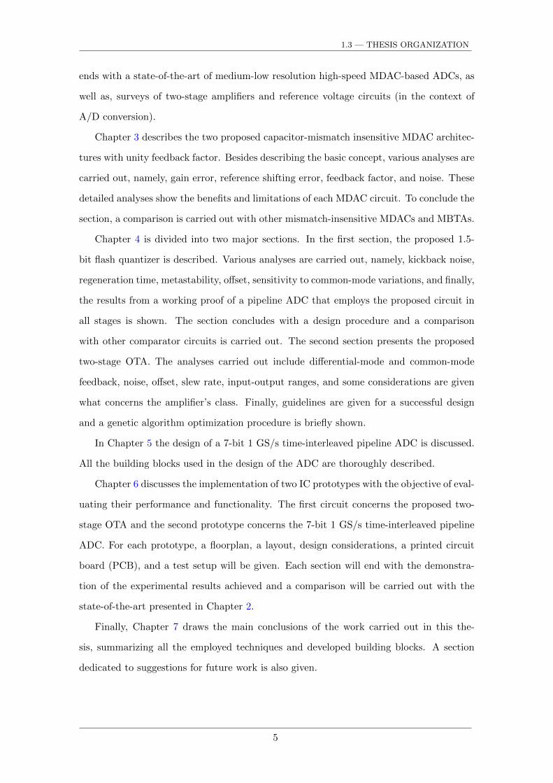
2.2.1 Two-Step Flash ADC
The Two-Step Flash architecture evolved from the Full-Flash converter. One of the main
drawbacks of the latter is the number of necessary comparators, given by Ncomp. = 2N −1,
which scales exponentially with the resolution of the converter, making it, in some cases,
impractical to implement due to the necessary die area. The Two-Step Flash topology
alleviates the number of necessary comparators by quantizing the input in two steps,
hence its name, as shown in Fig. 2.1a. The effective reduction factor in the number of
comparators when compared to the Full-Flash ADC, is exponentially proportional to the
converter’s resolution, and is approximately given by1 2N2−1. In other words, the higher
the resolution the more area efficient it becomes to use a Two-Step topology.
1Assuming that the same number of bits is extracted in both quantization steps, i.e. N1 = N2 = N/2.
8

2.2 — MDAC-BASED ANALOG-TO-DIGITAL CONVERTER ARCHITECTURES
S/H
N1-bit
DAC
+-
N1-bits N2-bits
G=2N1
G
MSBs LSBs
Vin
MDAC
res
N2-bit
QN1-bit
Q
ra
(a)
VREF
11
10
01
00
VREF
11
10
01
00
Vin ra
Am
plif
ica
tio
n
res
1st step 2
nd step
(b)
Á1
Á2
Sampling First step quantization
Residue amplification
Second step quantization
t1 t2 t
(c)
Figure 2.1: The Two-Step A/D converter: (a) Block diagram. (b) Example of residue am-plification. (c) Timing diagram.
As shown in Fig. 2.1a, each step (or stage) is composed of a quantizer, with a resolution
(N1 and N2) inferior to the resolution (N) of the entire converter, thus requiring less
reference voltages and comparators, and consequently, occupying less die area. Between
the two steps an amplified residue voltage needs to be generated, which is achieved with
a DAC, a subtraction operation block and a gain block. These three blocks constitute an
MDAC circuit. The principle of operation is as follows: the input is sampled by the first
quantizer during the sampling phase. During the residue amplification phase, the first
quantizer decides the most significant bits (MSBs), which are then used to reconstruct
a voltage (using the DAC), that is subtracted from the original sampled input and then
amplified (by 2N1) to create an amplified residue voltage. Still during this phase, the
second quantizer samples this residue. The objective of the amplification is to restore the
residue to the full voltage range of the converter, thus facilitating the implementation of
the second quantizer (Fig. 2.1b), or eventually, reusing the same quantizer in a cyclic way.
During the final phase, the second quantizer (of resolution N2) quantizes the residue to
obtain the least significant bits (LSBs). The final digital output is assembled using digital
9
Chapter 2 — GENERAL OVERVIEW OF PIPELINE ANALOG-TO-DIGITAL CONVERTERS
logic, by adding the MSBs together with the LSBs.
Basically, this topology simplifies the quantization, by trading comparators with time.
The Full-Flash converter achieves a quantization in two clock phases (one clock cycle),
while the Two-Step needs at least three phases, i.e., one and a half clock cycles (Fig. 2.1c).
Although the throughput may be similar to that of the Full-Flash converter (one digital
output per clock cycle), the Two-Step has higher latency2. If N1 is made equal to N2,
then only one quantizer needs to be designed and, therefore, both quantizers may use the
same reference voltages. The latter is also made possible by using a residue amplification
gain of 2N1 . The above assumptions consider that no digital redundancy is used.
If more steps (or stages) are added to the converter to simplify its implementation and
relax the requirements of each step, which would eventually lead to a minimum resolution
per step (N = 1), the resulting A/D architecture would be the Pipeline.
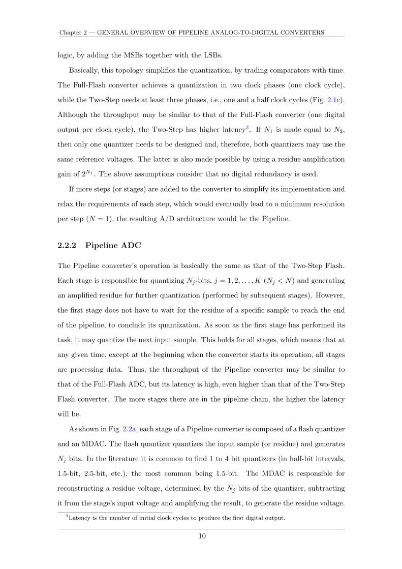
2.2.2 Pipeline ADC
The Pipeline converter’s operation is basically the same as that of the Two-Step Flash.
Each stage is responsible for quantizing Nj-bits, j = 1, 2, . . . ,K (Nj < N) and generating
an amplified residue for further quantization (performed by subsequent stages). However,
the first stage does not have to wait for the residue of a specific sample to reach the end
of the pipeline, to conclude its quantization. As soon as the first stage has performed its
task, it may quantize the next input sample. This holds for all stages, which means that at
any given time, except at the beginning when the converter starts its operation, all stages
are processing data. Thus, the throughput of the Pipeline converter may be similar to
that of the Full-Flash ADC, but its latency is high, even higher than that of the Two-Step
Flash converter. The more stages there are in the pipeline chain, the higher the latency
will be.
As shown in Fig. 2.2a, each stage of a Pipeline converter is composed of a flash quantizer
and an MDAC. The flash quantizer quantizes the input sample (or residue) and generates
Nj bits. In the literature it is common to find 1 to 4 bit quantizers (in half-bit intervals,
1.5-bit, 2.5-bit, etc.), the most common being 1.5-bit. The MDAC is responsible for
reconstructing a residue voltage, determined by the Nj bits of the quantizer, subtracting
it from the stage’s input voltage and amplifying the result, to generate the residue voltage.
2Latency is the number of initial clock cycles to produce the first digital output.
10

2.2 — MDAC-BASED ANALOG-TO-DIGITAL CONVERTER ARCHITECTURES
Stage 1
N1-bitVin
Stage j
Nj-bit
Stage K
NK-bit
ra1 raj
S/H
Nj -bit
DAC
+-
Nj -bits
G=2Nj
G
MDACresj
Nj -bit
Q
raj
(a)
t
Sample input (1)
Quantization
res1(1) amp.
Quantization
res2(1) amp.
Stage 1
Stage 2 Sample res1(1)
Sample input (2)
Quantization
res1(2) amp.
Sample res1(2)
Sample input (K)
Quantization
res1(K) amp.
Quantization
res2(K-1) amp.Sample res1(K)
Stage K Sample resK-1(1) Quantization
1 2 K
Clock Cycle
(b)
Figure 2.2: The Pipeline A/D converter: (a) Block diagram of a stage, exemplifying itsbuilding blocks. (b) Timing diagram.
This voltage is then held and passed onto the next stage where the stage’s operation is
repeated. The amplification of the residue, by 2Nj , is justified for increasing its dynamic
range to the full scale range of the converter, thus facilitating the implementation of
subsequent quantizers. Each stage’s operation is completed in two phases (one clock
cycle): the first for sampling and quantizing, and the second for residue amplification (see
the timing diagram of Fig. 2.2b).
Normally, all pipeline stages are designed with the same resolution to simplify the
converter’s layout and implementation, but, design trade-offs may determine that each
stage have different resolutions. It is usual to find the first stage with a higher resolution.
Another important reason for all stages to be equal (in resolution) is that the reference
voltages are the same for all quantizers and DAC functions.
What concerns digital logic, the Pipeline converter employs digital synchronization
logic to align (over time) all bits before producing the final digital output word. Aside
from synchronizing, these converters usually employ digital correction, which corrects for
11
Chapter 2 — GENERAL OVERVIEW OF PIPELINE ANALOG-TO-DIGITAL CONVERTERS
nonidealities in the flash quantizers [18]. The Two-Step Flash converter, described above,
may also employ digital correction logic. These digital blocks are detailed further on in
this chapter.
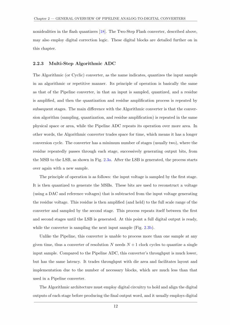
2.2.3 Multi-Step Algorithmic ADC
The Algorithmic (or Cyclic) converter, as the name indicates, quantizes the input sample
in an algorithmic or repetitive manner. Its principle of operation is basically the same
as that of the Pipeline converter, in that an input is sampled, quantized, and a residue
is amplified, and then the quantization and residue amplification process is repeated by
subsequent stages. The main difference with the Algorithmic converter is that the conver-
sion algorithm (sampling, quantization, and residue amplification) is repeated in the same
physical space or area, while the Pipeline ADC repeats its operation over more area. In
other words, the Algorithmic converter trades space for time, which means it has a longer
conversion cycle. The converter has a minimum number of stages (usually two), where the
residue repeatedly passes through each stage, successively generating output bits, from
the MSB to the LSB, as shown in Fig. 2.3a. After the LSB is generated, the process starts
over again with a new sample.
The principle of operation is as follows: the input voltage is sampled by the first stage.
It is then quantized to generate the MSBs. These bits are used to reconstruct a voltage
(using a DAC and reference voltages) that is subtracted from the input voltage generating
the residue voltage. This residue is then amplified (and held) to the full scale range of the
converter and sampled by the second stage. This process repeats itself between the first
and second stages until the LSB is generated. At this point a full digital output is ready,
while the converter is sampling the next input sample (Fig. 2.3b).
Unlike the Pipeline, this converter is unable to process more than one sample at any
given time, thus a converter of resolution N needs N + 1 clock cycles to quantize a single
input sample. Compared to the Pipeline ADC, this converter’s throughput is much lower,
but has the same latency. It trades throughput with die area and facilitates layout and
implementation due to the number of necessary blocks, which are much less than that
used in a Pipeline converter.
The Algorithmic architecture must employ digital circuitry to hold and align the digital
outputs of each stage before producing the final output word, and it usually employs digital
12

2.2 — MDAC-BASED ANALOG-TO-DIGITAL CONVERTER ARCHITECTURES
Stage 1
N1-bit
Stage 2
N2-bit
ra1 ra2
Vin
S/H
N1-bit
DAC
+-
N1-bits
G=2N1
G
MDACres1
N1-bit
Q
ra1
(a)
t
Sample input (1)
Quantization
res1(1) amp.
Quantization
res2(1) amp.
Stage 1
Stage 2 Sample res1(1)
Sample res2(1)
Quantization
res1(1) amp.
Sample res1(1)
Sample input (2)
Quantization
res1(2) amp.
Quantization Sample res1(2)
1 2 K
Clock Cycle
(b)
Figure 2.3: The Algorithmic A/D converter: (a) Block diagram. (b) Timing diagram.
correction logic.
In order to increase the throughput, the time-interleaved technique may be employed.
2.2.4 Time-Interleaving ADCs
Time-Interleaving [19] is a technique used to increase the throughput or conversion rate
of a converter. This technique may be applied to all A/D converter topologies. It consists
of using an array of M parallel converters multiplexed at the input and at the output as
shown in Fig. 2.4a. Each converter operates at a conversion rate FS/M , making it easier to
implement. The analog input multiplexer, adequately timed, is responsible for attributing
an input sample to each of the converters over time, when it reaches the last converter in
the array it starts over again. The digital output multiplexer guarantees that the timing
sequence of digital outputs are in accordance with the sampled inputs. Each converter
added to the array inevitably increases the die area and the power consumption of the
overall A/D conversion system. The timing diagram of operation is shown in Fig. 2.4b.
Besides the limitations produced by each unit (multiplexed) ADC, the time-interleaved
13

Chapter 2 — GENERAL OVERVIEW OF PIPELINE ANALOG-TO-DIGITAL CONVERTERS
ADC 1
@ FS/M
ADC 2
@ FS/M
ADC M
@ FS/M
Vin
@FS @FS
N
N
N
N
NDout
(a)
t
ADC 1
ADC 2
TS/M (M-1)TS/M
Clock Cycle
Sample and quantize input (M)
Sample and quantize input (1)
ADC M
Sample and quantize input (M+1)
Sample and quantize input (2) Sample and quantize input (M+2)
0 TS
(b)
Figure 2.4: Time-interleaving of A/D converters: (a) Block diagram. (b) Timing diagram.
technique introduces its own limitations. These have mainly to do with mismatches be-
tween the various unit ADCs that compose the converter [19–24]. This topology is very
sensitive to mismatches in the offset, gain, timing, and bandwidth, of each unit ADC.
No matter how bad the error of a unit ADC is, as long as all other units have the same
error magnitude, no mismatch will exist. All these errors cause a degradation of the
converter’s signal-to-noise ratio (SNR). A brief description of these errors is given next
and Table 2.1 presents a summary of the effects of time-interleaving mismatches [19–24].
For this discussion, a two-channel time-interleaved ADC will be used as an illustrative
example.
• Offset mismatch: contributes with a component at DC (frequency, f = 0) in the
output spectrum, which is already expected because all ADCs have an offset, but,
it also adds a spurious tone at half the sampling frequency (FS/2). The spectral
locations and the magnitude of these components are independent of input signal
amplitude and frequency.
• Gain mismatch: contributes with a spurious tone at half the sampling frequency
14

2.3 — MDAC-BASED ANALOG-TO-DIGITAL CONVERTER ARCHITECTURES
Table 2.1: Magnitude and spectral location of spurious tones due to mismatches and theireffect on the signal (Ain sin(2πfin)) component for a two-channel time-interleavedADC. The offset and gain mismatches are given by oi and gi respectively (i = 1, 2).The relative timing mismatch is given by ri = ∆ti/TS, where ∆ti is the absolutetiming mismatch and TS(= 1/FS) is the sampling period.
Mismatch Type Signal Component Spurious Component
(Magnitude) (Spectral location)
(Magnitude)
Offset —DC FS/2
o1+o22
o1−o22
Gain Aing1+g2
4
FS/2− fin
Aing1−g2
4
Timing Ain cos(2πfinr1−r2
2)
FS/2− fin
Ain sin(2πfinr2−r1
2)
Bandwidth see [23]FS/2− fin
see [23]
minus the input frequency (FS/2 − fin), thus its spectral location is dependent on
the input signal frequency. The magnitude of the spurious tone is only dependent
on the amplitude of the signal. The magnitude of the input signal is affected by this
mismatch.
• Timing mismatch: is due to variations in the sampling instant of each unit ADC, in
other words, differences in the relative time between samples taken. This mismatch
is similar to gain mismatch in the sense that it contributes with spurious tones at
the same spectral locations (FS/2 − fin), but, the magnitude is dependent on the
amplitude and the frequency of the signal. As with gain mismatch, timing mismatch
affects the magnitude of the input signal.
• Bandwidth mismatch: is due to differences in the sampling networks of each unit
ADC. If each unit ADC has a dedicated sample-and-hold (S/H), and if each S/H
has a different bandwidth, then bandwidth mismatch will affect the performance of
the overall time-interleaved ADC [22,23]. This mismatch adds similar contributions
to that of gain and timing mismatches. The main differences are that the gain part
of the bandwidth mismatch is now dependent on the input signal frequency and the
timing part has a nonlinear dependency with the input signal frequency.
15

Chapter 2 — GENERAL OVERVIEW OF PIPELINE ANALOG-TO-DIGITAL CONVERTERS
2.3 Building Blocks of Pipeline Analog-to-Digital
Converters
The objective of this section is to briefly overview each of the constituent blocks of a
Pipeline A/D converter. Besides an overview, errors related to each block will also be
given. Various references are given throughout the section for a more detailed coverage
and further reading. Note that, not all the blocks described below are necessary to build
a Pipeline ADC. For example, the sample-and-hold (S/H) and decimation blocks are not
strictly necessary. It should be equally noted that the blocks described below are generic,
in the sense that they are found in most Pipeline ADCs. In recent developments some of
these blocks have been substituted for more efficient ones and some have been eliminated
(mostly for power and/or area savings).
2.3.1 Sample-and-Hold
The sample-and-hold (S/H) block is found at the very beginning of the converter. Its
objective is to discretize, in time, i.e., to sample the input and hold the sampled input
for the subsequent block to process it. The S/H converts a continuous-time signal into
a discrete-time signal (the signal is still continuous in amplitude). Another circuit with
similar functions is a track-and-hold (T/H), where the main difference to a S/H is that the
output of the T/H tracks (follows) the input, then samples, and finally holds the sample.
A simple version of a S/H and a T/H are shown in Fig. 2.5 with their respective timing
diagram.
S/H circuits operate in two phases, the sampling and the holding phase, as shown
in Fig. 2.5a. During the sampling phase, the switch (φS) is closed and the capacitor
is charged to the input voltage. When the switch is opened, the input is sampled, and
because the charge on the capacitor can not be destroyed, the sampled voltage is held
on the capacitor. At this moment, the held voltage can only be sensed by a high input
impedance block such as an amplifier (unity-buffer in this case).
There are numerous errors associated to sampling and holding an input signal [25–27].
Some are mentioned below:
• Finite sampling bandwidth: if the input signal’s frequency is higher than the
sampling bandwidth (f−3dB = 1/(2πRSWCH)), an output signal voltage with a
16

2.3 — BUILDING BLOCKS OF PIPELINE ANALOG-TO-DIGITAL CONVERTERS
S S SH HÁS
Vin
Vout
S – Sample H – Hold
1Vin Vout
unity-buffer
ÁS
ÁS
ÁS
CH
SW
(a)
T T TH HÁT
Vin
Vout
T – Track H – Hold
1Vin Vout
ÁT
SW
CH
(b)
Figure 2.5: Simple versions of (a) S/H and (b) T/H, with output buffer and output waveform.
phase difference is sampled.
• Acquisition time: is the time it takes the amplifier (buffer) to settle. This error
is associated with amplifiers which will be explained further on.
• Sampling uncertainty (aperture error): is the time uncertainty at the moment
of sampling. This error has two possible origins: a long rise or fall time, or a sampling
instant that changes from period to period. This error is particularly problematic
in the presence of high frequency signals.
• Sampling pedestal: is the error voltage added to the sampled voltage caused by
the switch while it is turning off. This extra voltage is due to channel charge injection
and clock feed-through. This error is particularly problematic when the error voltage
is signal dependent, which adds distortion.
2.3.2 Multiplying-DAC
As seen in the previous section, the MDAC is a circuit which performs numerous functions.
These functions include sampling the input signal (or residue voltage from a previous
stage), reconstructing a voltage using a DAC, obtaining a residue (subtraction of the
reconstructed voltage from the stage’s sampled voltage), performing a gain to amplify the
residue, and finally holding the amplified residue for the next stage. The block diagram
of a generic MDAC is shown Fig. 2.6. Normally, a switched-capacitor (SC) network is
employed to accomplish all these functions. Sampling is achieved by means of switches
17
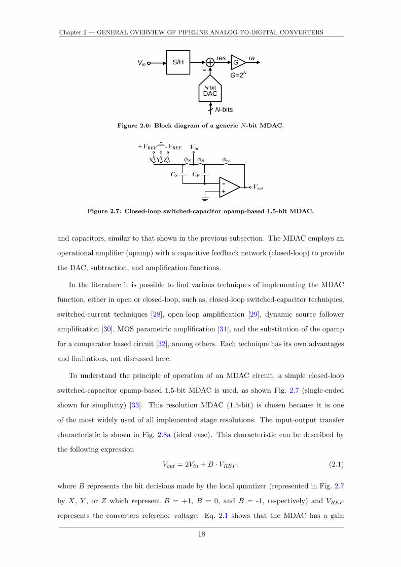
Chapter 2 — GENERAL OVERVIEW OF PIPELINE ANALOG-TO-DIGITAL CONVERTERS
+-
N-bits
G=2N
GVin
res ra
N-bit
DAC
S/H
Figure 2.6: Block diagram of a generic N-bit MDAC.
CF
Vout
Vin
CS
-+
-VREF+VREF
X Y Z ÁSÁS Ára
Figure 2.7: Closed-loop switched-capacitor opamp-based 1.5-bit MDAC.
and capacitors, similar to that shown in the previous subsection. The MDAC employs an
operational amplifier (opamp) with a capacitive feedback network (closed-loop) to provide
the DAC, subtraction, and amplification functions.
In the literature it is possible to find various techniques of implementing the MDAC
function, either in open or closed-loop, such as, closed-loop switched-capacitor techniques,
switched-current techniques [28], open-loop amplification [29], dynamic source follower
amplification [30], MOS parametric amplification [31], and the substitution of the opamp
for a comparator based circuit [32], among others. Each technique has its own advantages
and limitations, not discussed here.
To understand the principle of operation of an MDAC circuit, a simple closed-loop
switched-capacitor opamp-based 1.5-bit MDAC is used, as shown Fig. 2.7 (single-ended
shown for simplicity) [33]. This resolution MDAC (1.5-bit) is chosen because it is one
of the most widely used of all implemented stage resolutions. The input-output transfer
characteristic is shown in Fig. 2.8a (ideal case). This characteristic can be described by
the following expression
Vout = 2Vin +B · VREF , (2.1)
where B represents the bit decisions made by the local quantizer (represented in Fig. 2.7
by X, Y , or Z which represent B = +1, B = 0, and B = -1, respectively) and VREF
represents the converters reference voltage. Eq. 2.1 shows that the MDAC has a gain
18

2.3 — BUILDING BLOCKS OF PIPELINE ANALOG-TO-DIGITAL CONVERTERS
-VREF
Vout
Vin
+VREF0
-VREF
0
+VREFX Y Z
-VREF/4 +VREF/4
-VREF/2
+VREF/2
00 01 10 (Dout)
(a)
-VREF
Vout
+VREF0
-VREF
0
+VREF
-VREF/4 +VREF/4
-VREF/2
+VREF/2
(b)
-VREF
Vout
Vin
+VREF0
-VREF
0
+VREF
-VREF/4 +VREF/4
-VREF/2
+VREF/2
(c)
-VREF
Vout
Vin
+VREF0
-VREF
0
+VREF
-VREF/4 +VREF/4
-VREF/2
+VREF/2
(d)
-VREF
Vout
Vin
+VREF0
-VREF
0
+VREF
-VREF/4 +VREF/4
-VREF/2
+VREF/2
(e)
-VREF
Vout
Vin
+VREF0
-VREF
0
+VREF
-VREF/4 +VREF/4
-VREF/2
+VREF/2
(f)
Figure 2.8: Input-Output characteristics of the 1.5-bit MDAC and the effects of errors(dashed line represents the ideal situation): (a) Ideal. (b) Gain error: gain< 2. (c) Gain error: gain > 2. (d) Offset of the quantizer decision levels. (e)Offset in the MDAC due to charge injection or offset of the opamp. (f) DACnonlinearity.
component (2Vin) and a reference shifting component (B · VREF ).
Circuit operation is as follows: during φS the input (Vin) is sampled onto capacitors CS
and CF . During the residue amplification phase (φra), CF is put in the opamp’s feedback
loop, and, due to charge conservation, the charge on CS is transferred to CF . The amount
of transferred charge depends on the quantizer’s decision (X, Y , or Z). If Y is high, i.e.,
if the Y switch is closed, the sampled input charge on CS is transferred to CF . In this
case the output (Vout) will simply be 2Vin (parameter B of Eq. 2.1 is 0). If X or Z is
enabled, then there will respectively be a charge addition or subtraction on CS and the
resultant charge transferred to CF . In this single-ended version example, the DAC is only
composed of capacitor CS .
The limiting factors of closed-loop SC-MDAC circuits are given next. To aid the
enumeration of these factors, the example of the 1.5-bit MDAC will be used as well as its
transfer characteristics shown in Fig. 2.8.
• Gain error: caused by capacitor mismatch (between CS and CF ) and finite opamp
DC gain [18,34,35]. Slopes of the characteristic vary from the ideal value of 2. See
19

Chapter 2 — GENERAL OVERVIEW OF PIPELINE ANALOG-TO-DIGITAL CONVERTERS
Fig. 2.8b and 2.8c.
• Offset errors: can be caused by offset of the quantizer decision levels (Fig. 2.8d), by
charge injection [36], or by opamp offset in the MDAC (Fig. 2.8e). Offset errors are
of minor importance given that most errors can be corrected by the digital correction
logic [18].
• Nonlinearity errors: caused by DAC capacitor mismatch and nonlinearity errors
present in the opamp [35] (Fig. 2.8f).
• Thermal noise: comes from the ON-resistance of the switches which is sampled on
the sampling capacitors and from the opamp [34].
• Speed: conversion rate is limited by the opamp’s closed-loop configuration, namely,
the opamp’s finite speed (GBW) and the closed-loop feedback factor [33] (slew rate
may also be a limiting factor of the speed).
2.3.3 Local Flash Quantizer and Comparators
As the name indicates, this circuit is a quantizer based on the Full-Flash converter topol-
ogy. In Fig. 2.9a, a generic N -bit flash quantizer is shown. It employs, in parallel, a
number of comparators3, each with their own reference voltage, to be compared with the
input signal. The output of each comparator is either 0 or 1, indicating that the input sig-
nal’s voltage is lower or higher than the reference voltage, respectively. There are various
methods of implementing the comparator: cascade of inverters (or simple gain stages),
an opamp in open-loop, and the latched comparator [25,37]. The first two circuits are
designed to amplify the input signal or the difference between the input and reference
signals to guarantee a logic output (0 or 1, or, in terms of voltage, the negative or positive
saturation voltage, respectively). The latched comparator is composed of a pre-amplifier
and a positive feedback latch. The pre-amplifier amplifies the small differential input sig-
nal and minimizes effects caused by the latch, while the latch guarantees logic levels at
the comparator’s output.
In Fig. 2.9b, the last block of the 1.5-bit flash quantizer is an XYZ encoder. This
circuit is responsible for guaranteeing, depending on the decisions of the comparators,
3The comparator is probably the most widely used component in A/D conversion, fundamental inpractically all topologies.
20
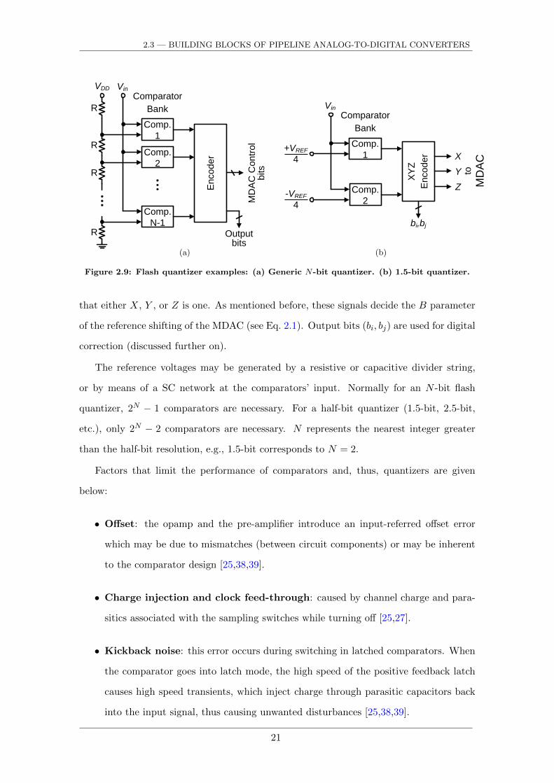
2.3 — BUILDING BLOCKS OF PIPELINE ANALOG-TO-DIGITAL CONVERTERS
Comp.
1
En
co
de
r
Comparator
Bank
Comp.
2
Comp.
N-1
MD
AC
Co
ntr
ol
bits
VDD Vin
R
R
R
R Outputbits
Comp.
1
XY
Z
En
co
de
r
Comparator
Bank
Comp.
2
Vin
X
Y
Z
+VREF
4
-VREF
4
to
MD
AC
bi,bj
(a) (b)
Figure 2.9: Flash quantizer examples: (a) Generic N-bit quantizer. (b) 1.5-bit quantizer.
that either X, Y , or Z is one. As mentioned before, these signals decide the B parameter
of the reference shifting of the MDAC (see Eq. 2.1). Output bits (bi, bj) are used for digital
correction (discussed further on).
The reference voltages may be generated by a resistive or capacitive divider string,
or by means of a SC network at the comparators’ input. Normally for an N -bit flash
quantizer, 2N − 1 comparators are necessary. For a half-bit quantizer (1.5-bit, 2.5-bit,
etc.), only 2N − 2 comparators are necessary. N represents the nearest integer greater
than the half-bit resolution, e.g., 1.5-bit corresponds to N = 2.
Factors that limit the performance of comparators and, thus, quantizers are given
below:
• Offset: the opamp and the pre-amplifier introduce an input-referred offset error
which may be due to mismatches (between circuit components) or may be inherent
to the comparator design [25,38,39].
• Charge injection and clock feed-through: caused by channel charge and para-
sitics associated with the sampling switches while turning off [25,27].
• Kickback noise: this error occurs during switching in latched comparators. When
the comparator goes into latch mode, the high speed of the positive feedback latch
causes high speed transients, which inject charge through parasitic capacitors back
into the input signal, thus causing unwanted disturbances [25,38,39].
21
Chapter 2 — GENERAL OVERVIEW OF PIPELINE ANALOG-TO-DIGITAL CONVERTERS
• Comparison time: this is the time the comparator takes to produce a valid digital
output. The worst case scenario is described by an overdrive recovery test, which
defines the time the comparator takes to recover from a large input immediately
followed by a very small input [38,40].
• Metastability: occurs when a very small input renders the comparator to be unable
to produce a valid digital output. This error may be given as a probability of the
occurrence of a metastable state [38,41], as a number of metastable states per second
[27], or, for the case of a flash quantizer with various comparators, as the mean time
between failures (taking into account the number of comparators) [42].
2.3.4 Operational Amplifier and Common-Mode Feedback Circuitry
The operational amplifier, better known as opamp, is probably the most important and
most used block in analog signal processing. The word operational comes from the fact that
these blocks can be used to implement various functional operations. It is an active circuit
which ideally has high gain, high input impedance, and low output impedance. Typically
working in the voltage domain, a voltage is inputted and an amplified voltage is provided
at the output, i.e., the opamp is a voltage-controlled voltage source (Vout = A×(V +−V −),
where A is the opamp’s open-loop gain), as shown in Fig. 2.10a. There are more types of
amplifiers, but the one that deserves attention, given the work developed in this thesis, is
the operational transconductance amplifier (OTA). This type of amplifier achieves a high
open-loop gain (at low frequencies) at the expense of a high output impedance. They are
widely used in SC circuits and do not need low output impedance because they usually
only drive pure capacitive loads (and not resistive loads). Their gain and speed depend
on the transconductance of specific transistors that compose the OTA.
Opamps usually operate in closed-loop form, inheriting all the associated benefits such
as, less sensitivity to circuit and process, supply voltage, and temperature (PVT) varia-
tions, thus less distortion, higher input impedance, lower output impedance, and higher
bandwidth. Fig. 2.10b depicts a simplified block diagram of a negative closed-loop system,
where A(s) represents the opamp’s open-loop gain (it represents Fig. 2.10a), β(s) is the
feedback network (with associated feedback factor), and s is the complex frequency.
As an example of the functionality and importance of the opamp, the SC circuit
22

2.3 — BUILDING BLOCKS OF PIPELINE ANALOG-TO-DIGITAL CONVERTERS
Vout
V+
V–
Zin Zout
A×(V+-V–)-
+
-+
Ideally: Zin = ∞Zout = 0
A = ∞
(a)
A(s)
β(s)
+ Vout(s)Vin(s)-
(b)
Figure 2.10: Opamp: (a) Basic symbol. (b) Simplified block diagram of a feedback circuit.
of Fig. 2.11a is used (this circuit is similar to Fig. 2.7 for Y = 1). For this example
CL represents a load capacitor and the objective is to double the input voltage (i.e.,
Vout = 2Vin). During φ1, Vin is sampled onto CS and CF . During φ2, the opamp (in
closed-loop now) forces a virtual ground at its inverting input and, hence the voltage
across CS to zero. Due to charge conservation, the charge stored on CS , QS = CSVin, is
transferred to CF . No charge goes to the amplifier because of its high input impedance.
If CF equals CS then Vout becomes 2Vin. Another way of exemplifying the importance of
the opamp is: during φ1, the voltages at the top and bottom plates of CS are Vin and zero,
respectively. Immediately at the beginning of φ2, the top plate of CS is connected to zero,
which forces its bottom plate (and the opamp’s inverting input) to −Vin. Simultaneously,
the opamp (in closed-loop now) forces the virtual ground at its inverting input. In order to
accomplish the virtual ground, the output voltage has to be increased by the same amount
of voltage, i.e., Vin. Finally, the output will become 2Vin at the end of φ2. If no opamp is
used in the aforementioned explanations, neither charge conservation nor virtual ground
would occur. Consequently, the sampled charge would simply be distributed between CS ,
CF , and CL, but Vout would not be 2Vin at the end of φ2.
Fig. 2.11b illustrates the equivalent block diagram of the SC circuit of Fig. 2.11a, where
the feedback network is given by β(s) = CF /(CF + CS + cip) and the input network is
λ(s) = (CS + CF )/(CF + CS + cip) [43].
At the transistor level, many amplifier architectures exist. It will not be the objective
of this work to describe any, but rather to give an idea of the common blocks used in most
of them. The basic blocks are an input stage (where the input signal is connected), a gain
or differential to single-ended conversion stage, and finally, an output driver stage (used
to drive the load connected at the output) [37]. It is possible that the input and output
stages be differential, thus inheriting the advantages of fully differential circuits, which will
23

Chapter 2 — GENERAL OVERVIEW OF PIPELINE ANALOG-TO-DIGITAL CONVERTERS
CF
Vout
Vin
CS
-+CL
Á2 Á2Á1Á1
Á1 cip
(a)
A(s)
β(s)
+ Vout(s)Vin(s)-
λ(s)
(b)
Figure 2.11: Example using an opamp in a feedback loop: (a) SC circuit. (b) Simplifiedblock diagram of the feedback scheme.
be given further on. When supply voltages were high (higher than 1.8 V in older CMOS
technology nodes), gain was achieved by cascoding (stacking) transistors. In this case
enough gain was achieved with a single-stage amplifier, which also has the highest speed
of operation. However, due to the power reduction necessity and low supply voltage (1.2 V
and lower) tendency of modern nanoscale CMOS technologies (0.13 µm and beyond), it is
no longer possible to cascode transistors, therefore, gain can only be achieved by multiple
stages, i.e., by cascading stages. Besides gain, the output swing also decreases due to the
supply voltage reduction, thus another reason to cascade stages. At this moment, we have
arrived at a two-stage amplifier: the first stage mainly for gain and the second for output
swing and speed with a small contribution to the overall gain. Due to compensation (to
stabilize the amplifier), which is inevitable, the speed of the two-stage amplifier is reduced
when compared to its single-stage counterpart. If more gain is needed, another stage can
be added (three-stage amplifier), at the expense of speed and stability issues.
There are a number of parameters that characterize the performance of opamps. Most
of these are limiting factors of their performance. Depending on the application the opamp
is inserted in, some become more relevant than others. Here most of them will be described
[25,40,44–46]. The parameters are:
• Low-frequency gain: There are two types of gains, differential-mode (DM) and
common-mode (CM) gain. Usually an opamp is sized for a given DM gain while
minimizing the CM gain. The former is fundamental as it determines the preci-
sion of the overall system where the opamp is used (usually in closed-loop). These
gains, measured with the opamp in open-loop, are a function of frequency. At low
frequencies they are called, the DC gain. An important sub-parameter of gain is
its nonlinearity for different output voltages. Normally, for a small output voltage
24

2.3 — BUILDING BLOCKS OF PIPELINE ANALOG-TO-DIGITAL CONVERTERS
swing, the gain has its maximum value, but for larger voltage swings, the gain tends
to be smaller.
• Bandwidth: There are two types of bandwidths, small-signal and large-signal (dis-
cussed in the following item), which characterize the high frequency performance
of opamps. The former is related to the frequency dependence of the open-loop
gain, which is caused by parasitic, compensation, and/or load capacitors present
in the opamp. The open-loop gain versus frequency, has a constant value for low
frequencies (DC gain, explained before) and then at a certain point in the frequency,
the gain starts to decrease or roll-off (at a -20 dB/decade rate). This point is the
opamp’s bandwidth or the location of the dominant pole. The point at which the
gain reaches unity is the unity gain bandwidth (fu) or the gain-bandwidth product
(GBW). Note that, GBW = fu is only applicable either for a single pole opamp or for
an adequately compensated multi-pole opamp [40,45]. These two design parameters,
fu and GBW, determine the speed of the system the opamp is inserted in.
• Slew rate: or large-signal bandwidth determines the rate at which the opamp can
change the output voltage in the presence of large input signals. In large signal
conditions, the opamp will try to provide current to charge the capacitors (compen-
sation, load, etc.) of the system. The rate at which it does this is called the slew
rate (SR). If the current is insufficient or the opamp does not have enough time (case
of SC circuits) to charge the capacitors, the output will not reach the desired value
and nonlinear distortion will arise.
• Compensation and Phase Margin: Opamps inserted in feedback loops can be
potentially unstable, if not adequately compensated. A measure of this instability
is called phase margin (PM). In single-stage opamps (which are less prone to insta-
bility), compensation is normally achieved (almost for free) by the load capacitor.
In multi-stage opamps (unstable by nature), compensation capacitors and compen-
sation schemes are inevitable.
• Settling time: This defines the time it takes the output to reach its final value
within a given settling error (associated with the desired accuracy) when a step
input is applied. This is probably the most important opamp parameter for SC
25

Chapter 2 — GENERAL OVERVIEW OF PIPELINE ANALOG-TO-DIGITAL CONVERTERS
t
Vout
y=ax(a>1)y=ax(a<1)Gain
Gainnonlinearity
Slew rate
β,GBW, and PM
Chargeredistribuition
Settlingaccuracy
Input step
Output response
Figure 2.12: Time-domain opamp output response (to an input step) and the role played bysome opamp performance parameters.
circuits given that it is a time domain parameter, that includes the effect of gain
(and its nonlinearity), small-signal bandwidth, slew rate, phase margin, and the
closed-loop’s feedback factor. Fig. 2.12 [47] depicts an opamp’s output response to
an input step showing where each mentioned parameter plays its role. If any of them
are not designed correctly, their effects will be pronounced in the output response
and a longer settling time will probably occur.
• Output swing: is the maximum output voltage range possible that maintains the
opamp functioning nominally, i.e., with the desired gain.
• Common-mode input range: is the maximum input voltage range that guaran-
tees negligible degradation of the opamp’s performance.
• Offset: is the output voltage when the input is zero. Ideally the output voltage
should be zero, but will not be due to inherent design issues of the opamp (systematic
offset) and mismatches between otherwise matched transistors (random offset). This
offset voltage, if large enough, can limit the output swing.
• Noise: is generated by devices with resistive components such as transistors (resis-
tive channel) and, naturally, resistors. There are many types of noise, the two most
commonly discussed are flicker (or 1/f) and thermal noise. The latter is of more
importance in high-speed or wideband opamps. Just as in the case of offset, the
opamp may be designed for low noise but never for zero noise. Noise determines the
smallest detectable input, the opamp may process.
Most parameters can be enhanced by using a fully differential structure for the opamp.
26

2.3 — BUILDING BLOCKS OF PIPELINE ANALOG-TO-DIGITAL CONVERTERS
In fact, opamp performance can double. This type of structure indicates that the opamp,
besides having a differential input, also has a differential output. The advantages of the
fully differential architecture are well known and are: larger gain, larger output swing,
higher immunity to extrinsic noise, reduced distortion (suppression of even harmonics)
and enhanced speed/power ratio [48]. Although the intrinsic noise level of fully differential
circuits is higher, the signal-to-noise ratio (SNR) will still be higher than single-ended
output circuits due to the larger output swing obtained.
An opamp designed with a fully differential structure needs to employ a special circuit
to measure and control its output common-mode voltage. This circuit is known as the
common-mode feedback (CMFB) circuit. Without this circuit the uncontrolled output CM
voltage could drift to the supply rails. The CMFB circuit guarantees that this voltage
stays approximately at midway between the supply rails. There are continuous-time and
SC-CMFB circuits. Usually in SC circuits, the SC version of CMFB circuits is preferred.
2.3.5 Reference V/I and Buffering
Reference circuits are essential in analog and data converter systems. They generate
reference voltages and currents that are used to bias circuits, to compare with other
signals, for addition and subtraction operations, among others. In the specific case of data
converters, reference circuits are determinant in defining the input and output full-scale
ranges. Therefore it is necessary to guarantee a sufficient level of accuracy4, so that the
overall performance of the data converter is not limited. To achieve this, they need to
be independent of external conditions such as, process, supply voltage, temperature, and
load disturbances. In the case where a reference voltage needs to drive a large capacitor
or various capacitors amounting to a large capacitance (like in DAC circuits), or be used
in a high-speed or high-accuracy SC circuit, an additional block needs to be added to the
output of the reference circuit. Commonly known as a reference buffer, this block is used
to maintain the reference voltage constant and to guarantee that it charges and discharges
the capacitors it drives, in the available amount of time (particular case of SC circuits).
In other words, the buffer must settle the reference voltage to within a given error, within
a given time slot, which depends on the accuracy and speed of the converter.
4In [49] it is shown that the reference circuit can have 1-bit lower accuracy than the resolution of theADC.
27

Chapter 2 — GENERAL OVERVIEW OF PIPELINE ANALOG-TO-DIGITAL CONVERTERS
There are many forms of generating a reference voltage (resistive or capacitive lad-
ders, bandgap circuits, etc.), but this is not the objective of this subsection. Instead, an
overview of the issues and difficulties designers have to overcome to buffer and/or stabilize
a reference voltage for SC converters, will be given.
It is possible to find many forms of reference voltage schemes in the literature. The
options divide into on- and off-chip buffering with (or without) the use of on- and off-chip
damping resistors and decoupling capacitors. The following table describes and analyses
the most used forms of reference voltage circuitry and buffering schemes.
Table 2.2: Description and analysis of the advantages and disadvantages of different referencevoltage schemes.
Description Analysis Diagram Performance
On-chip
buffer
without
decoupling
[50–53]
• High-speed buffer with wide
bandwidth.
• High power consumption.
• Noise performance hard to
achieve (as frequency rises,
buffer output impedance
rises).
• [51] uses a deglitch circuit
to minimize glitches during
switching.
• Due to large current peaks,
the buffer may require dedi-
cated supply pins.
Ref.
circuit
off-chip on-chip
VREFBuffer
FreePad/Pin
to ADC
• Accuracy ;
• Power
• Speed ;
• On-chip area ;
• Off-chip area ;
continued on next page . . .
28

2.3 — BUILDING BLOCKS OF PIPELINE ANALOG-TO-DIGITAL CONVERTERS
Description Analysis Diagram Performance
On-chip
buffer with
internal
decoupling
[54–56]
• Wirebond inductance too
large for off-chip decoupling
due to impractical amount of
ringing on reference voltage.
• Large on-chip capacitors, oc-
cupying large area, are un-
avoidable [55].
• On-chip RC filter [56].
Ref.
circuit
off-chip on-chip
Bufferto ADC
Cint
FreePad/Pin
• Accuracy ;
• Power ;
• Speed ;
• On-chip area
• Off-chip area ;
On-chip
buffer with
external
decoupling
[57–61]
• Low bandwidth buffer.
• Low power consumption.
• Noise performance and out-
put impedance dependent on
quality (ESL and ESR) of de-
coupling capacitors.
• Wirebond inductance causes
ringing of the internally
generated reference voltage.
Dampen ringing with large
on-chip capacitors and re-
sistors (these occupy large
area).
• Reduce inductance with spe-
cial packaging†[57].
• Additional pins.
Ref.
circuit
off-chip on-chip
Bufferto ADC
Cext
L
(C >>)
Wirebond • Accuracy ;
• Power ;
• Speed
• On-chip area ;
• Off-chip area
continued on next page . . .
29
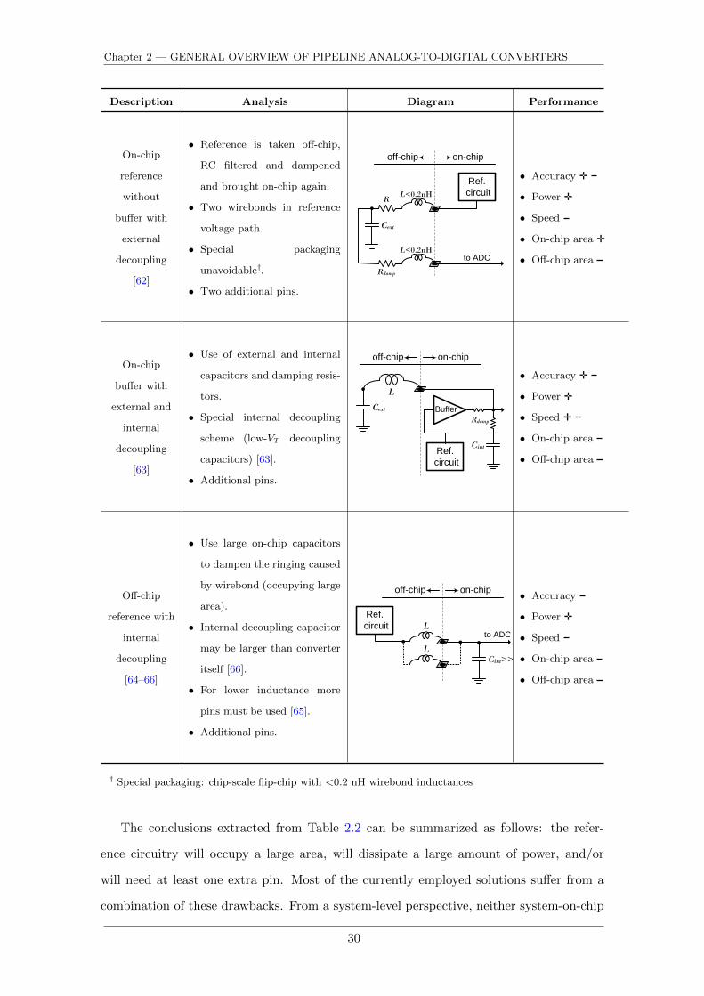
Chapter 2 — GENERAL OVERVIEW OF PIPELINE ANALOG-TO-DIGITAL CONVERTERS
Description Analysis Diagram Performance
On-chip
reference
without
buffer with
external
decoupling
[62]
• Reference is taken off-chip,
RC filtered and dampened
and brought on-chip again.
• Two wirebonds in reference
voltage path.
• Special packaging
unavoidable†.
• Two additional pins.
Ref.
circuit
off-chip on-chip
to ADC
Cext
L<0.2nH
L<0.2nH
R
Rdamp
• Accuracy ;
• Power ;
• Speed
• On-chip area ;
• Off-chip area
On-chip
buffer with
external and
internal
decoupling
[63]
• Use of external and internal
capacitors and damping resis-
tors.
• Special internal decoupling
scheme (low-VT decoupling
capacitors) [63].
• Additional pins.
Ref.
circuit
off-chip on-chip
Cext
L
Cint
Rdamp
Buffer
• Accuracy ;
• Power ;
• Speed ;
• On-chip area
• Off-chip area
Off-chip
reference with
internal
decoupling
[64–66]
• Use large on-chip capacitors
to dampen the ringing caused
by wirebond (occupying large
area).
• Internal decoupling capacitor
may be larger than converter
itself [66].
• For lower inductance more
pins must be used [65].
• Additional pins.
Ref.
circuit
off-chip on-chip
to ADCL
Cint>>L
• Accuracy
• Power ;
• Speed
• On-chip area
• Off-chip area
† Special packaging: chip-scale flip-chip with <0.2 nH wirebond inductances
The conclusions extracted from Table 2.2 can be summarized as follows: the refer-
ence circuitry will occupy a large area, will dissipate a large amount of power, and/or
will need at least one extra pin. Most of the currently employed solutions suffer from a
combination of these drawbacks. From a system-level perspective, neither system-on-chip
30

2.3 — BUILDING BLOCKS OF PIPELINE ANALOG-TO-DIGITAL CONVERTERS
nor system-in-package designs are benefitted from voltage-domain reference circuitry. To
avoid extra costs, no extra pins can be used, therefore, on-chip high-speed buffering must
be employed, a trade between cost and power is made. If extra pins are available, then
off-chip decoupling may be used (with a low bandwidth buffer), but then a penalty in area
is paid for the off-chip decoupling capacitors. All this to avoid on-chip decoupling because
silicon area is more expensive (valuable) than discrete components.
Parameters of reference circuits and buffers that may affect the overall performance of
data converters are given next. They are:
• Ringing: is caused by the inductance (L) of the wirebond and converter’s ca-
pacitance (C) during switching in SC circuits. The ringing occurs at the natural
frequency of the LC circuit. To reduce and dampen the ringing, large on- and/or
off-chip decoupling capacitors and damping resistors must be used [49,64,66,67].
• Speed: of a reference circuit or buffer is determinant in the presence of perturba-
tions [44]. During clocking of the capacitors in SC circuits, the reference voltage
is constantly disturbed, and has to recover before the end of the phase to avoid
incomplete reference settling which causes offset errors. This error may limit the
converter’s conversion rate.
• Output Impedance: it is fundamental that the output impedance of the buffer
circuit be as low as possible, to adequately feed the converter with the reference
voltage, avoiding large voltage drops. To achieve low output impedance at high
frequencies, large capacitors need to be used, which consequently occupy a large
amount of area. Nevertheless, large capacitors help reduce the noise bandwidth and
suppress external disturbances, if large enough [44].
• Noise: directly couples to the stage’s input signal during sampling and also to the
output signals during the amplification phase. Because noise limits the smallest sig-
nal that may be converted, it directly influences the full-scale range of the converter
[49].
• PSR: power supply rejection determines the capacity of the buffer to reject noise of
the supply (VDD and ground) lines from coupling to the output buffered voltage. If
noise couples to the output voltage, it contributes to the total output noise of the
31

Chapter 2 — GENERAL OVERVIEW OF PIPELINE ANALOG-TO-DIGITAL CONVERTERS
buffer.
• Offset: errors limit the full-scale range of the converter. Negative offsets (lower
reference voltage) saturate the residue voltage, thus reducing the conversion range,
which causes distortion. Positive offsets (higher reference voltage) cause residue
voltages to be smaller thus degrading the signal-to-noise ratio (SNR) of the converter
[49]. These offset errors cause interstage gain errors [58] and overall converter gain
errors.
• Signal dependency: when a reference voltage and input signal are connected to
the capacitor’s plates, any variation in one signal causes a modulation in the other.
This is called signal-dependent modulation. Therefore, if a reference voltage does not
settle adequately, it induces a variation in the input signal, which is then sampled.
This modulation degrades the performance of the converter [49], [58].
• Reference distribution: is not an easy task, particularly when references must be
provided to widely separated locations across the die [68], or in converters with high
clock rates or high resolutions [62]. The long lines cause voltage drops which alter
the reference’s original value. If each pipeline stage uses a reference voltage with a
different value, the performance of the converter is highly degraded.
2.3.6 Clock Generation
Switched-capacitor circuits need clocking schemes to turn on/off the circuit’s switches to
achieve a specific function. Most data converters rely on a special scheme that permits
the signal acquired during the sampling phase to be transferred and amplified without
loss. In other words, it is imperative that no charge is destroyed or lost between the
sampling and amplification phases. To achieve this, the overlapping time between phases
must be zero. This is accomplished by a nonoverlapping clock generator. An example of a
simple two-phase nonoverlapping clock generator, widely found and used in the literature,
is shown in Fig. 2.13 [41]. This simple configuration has one clock input and two phases
with 180 phase shift are provided at the output. The nonoverlapping time is controlled
by the delay of the input NAND gate and the two inverters (before the feedback). To
increase this time, more inverters (in an even number) can be added.
32

2.3 — BUILDING BLOCKS OF PIPELINE ANALOG-TO-DIGITAL CONVERTERS
nonoverlapping
time
TCLK
t
tCLK
@
FS
VDD
VSS
Á1@FS
Á2@FS
transmissiongate
Figure 2.13: Simple two-phase nonoverlapping clock generator and output waveforms.
There are other schemes of generating nonoverlapped phases, namely using phase-
locked loops [69] or delay-locked loops [70]. These circuits are much more complex than
the simple two-phase nonoverlapping clock generator of Fig. 2.13. They are used in many
applications such as in communication, data and clock recovery, FM demodulation, and
high-speed or high-resolution data converters, among others. Given that they were not
used in the work developed in this thesis, they will not be further discussed.
Clock generation or clock synthesis circuits limit the performance of data converters
due to PVT variations, but mainly due to device and delay mismatches. These circuits
contribute the following errors:
• Clock jitter: is the random variation of the time the clock falls to zero (the falling
edge is used here to define the sampling instant) around the ideal time. This error
was briefly covered in the S/H subsection. The jittering of the timebase translates
into an increase of the noise floor over all frequencies, and consequently, degrades
the SNR of the converter. As mentioned before, this error is input signal dependent.
• Clock skew: is a fundamental limitation inherent to time-interleaved converters.
Each unit converter of a time-interleaved topology must sample the input at equally
spaced instants in time, given by the M/FS , where M is the number of unit con-
verters and FS is the total sampling frequency. Any deviation from these ideally
spaced sampling instants causes timing errors, which translate into deterministic
spurious tones (visible in the converter’s output spectrum), ultimately degrading
the SNR of the converter. This error is also input signal dependent and was covered
in Section 2.2.4 (timing mismatch).
33

Chapter 2 — GENERAL OVERVIEW OF PIPELINE ANALOG-TO-DIGITAL CONVERTERS
2.3.7 Digital Backend and Decimation
As mentioned in Section 2.2 for the various topologies, a backend only composed of digital
circuits is necessary. These circuits store and align the digital outputs from each stage,
which then move on to the correction stage, and are finally buffered to produce the final
digital output word. Basically three digital blocks are necessary: synchronization logic,
digital correction logic, and output buffers. The latter block (which is basically an even
number of cascaded inverters) is optional and depends on where the digital outputs need
to go next and if they need to be buffered or not. To exemplify the functionality of the
circuits described in this subsection, a simple 4-bit Pipeline converter with two 1.5-bit
stages and a final 2-bit stage will be used.
Synchronization logic is fundamental in converters that are unable to produce a digital
word in one clock cycle, i.e., are unable to digitize the analog input at once (like Full-
Flash converters). This logic is mainly composed of memory and shift circuits, such as
flip-flops (FF) or shift registers. Taking the example of Fig. 2.14, when the analog input
signal is processed by the first stage, its comparator produces digital outputs which need
to be stored because the residue voltage will only be processed by the last stage of the
converter at the end of one more cycle. Therefore, during this clock cycle, the bits from
the first stage need to be stored. The same analysis can be made for the outputs of the
second stage, which need to be stored for half a clock cycle. As can be seen in Fig. 2.14a,
FFa and FFb synchronize the digital outputs, while FFc−e align the outputs of a specific
input sample for later processing. Fig. 2.14b shows the timing diagram of operations and
time-alignment, i.e., where the digital outputs of each of the sampled inputs are aligned
at a specific instance in time. After all digital outputs are time-aligned they are ready for
digital correction.
Digital correction logic is used to correct nonidealities and indecisions in the compara-
tors used in the quantizers [18,33]. Therefore, the quantizer’s offsets can be as large as
1/2VLSB = VREF /4 for a 1.5-bit stage, which relaxes the specifications of the quantizer.
This correction logic works on the basis that each stage has redundancy which is used for
correction and eliminated by the correction logic itself. For example, a 1.5-bit stage has
a true resolution of 1-bit and 0.5-bit redundancy. It has two digital output bits as shown
by the input-output characteristic of Fig. 2.8a, where possible digital outputs are 00, 10,
34

2.3 — BUILDING BLOCKS OF PIPELINE ANALOG-TO-DIGITAL CONVERTERS
Stage 1
1.5-bitVin
Stage 2
1.5-bit
Stage 3
2-bit
ra1 ra2
FF(x2)
FF(x2)
FF(x2)
FF(x2)
FF(x2)
Q1 Q2 Q4Q3
CLK
to next digital block ...
a
b
c d e
Syn
ch
ron
iza
tio
nT
ime
-a
lign
me
nt
2
2
2 2
2
2
(a)
S1(1)Q1(1)
ra1(1)S1(2)
Q1(2)
ra1(2)S1(3)
Q1(3)
ra1(3)Stage 1
S2(1)Q2(1)
ra2(1)S2(2)
Q2(2)
ra2(2)S2(3)
Q2(3)
ra2(3)Stage 2
S3(1) Q34(1) S3(2) Q34(2) S3(3) Q34(3)Stage 3
Q1(1)FFa
FFb
FFc
FFd
FFe
Q1(2) Q1(3)
Q2(1) Q2(2) Q2(3)
Q1(1) Q1(2) Q1(3)
Q2(1) Q2(2) Q2(3)
Q34(1) Q34(2) Q34(3)
t
Quantization of sample (1) time-aligned
Quantization of sample (3) time-aligned
Quantization of sample (2) time-aligned
(b)
Figure 2.14: Simple example of synchronization: (a) Pipeline converter, synchronization andtime-alignment logic. (b) Time scheme of operations.
and 01. The 00 output indicates that the sampled input is certainly negative, while the
10 output indicates that it is certainly positive. The 01 output indicates indecision, i.e.,
the quantizer does not know if the sampled input is either positive or negative [41]. This
decision is postponed to subsequent stages and the correction logic (with the digital out-
puts of these stages) will correct this indecision. All this is only possible if the quantizer’s
offsets are less than 1/2VLSB.
An example of how correction logic operates is shown in Fig. 2.15. In Fig. 2.15a, an
35

Chapter 2 — GENERAL OVERVIEW OF PIPELINE ANALOG-TO-DIGITAL CONVERTERS
+0.5
0-0.125
V
+0.125
-0.5
Stage1 Stage2 Stage3
Vin = 0.1V
-0.250
+0.2500.2
-0.1
00
01
10 11
00
01
10
1.5-bit 1.5-bit 2-bit
0 1 1 0 0 1
+++
1001
00
01
10
MSB LSB
(a)
+0.5
0-0.125
V
+0.125
-0.5
Stage1 Stage2 Stage3
Vin = 0.1V
-0.250
+0.2500.2
+0.4
00
01
10 11
00
01
10
1.5-bit 1.5-bit 2-bit
0 1 0 1 1 1
+++
1001
00
01
10
MSB LSB
(b)
Figure 2.15: Example of the operation of digital correction: (a) Ideal situation (and indeci-sion corrected). (b) Offset error in stage 2: offset corrected.
ideal situation is depicted, i.e., the comparators do not have offsets. In Fig. 2.15b, one
of the comparators of stage 2 has a positive offset (indicated by the curly arrow). Even
though there is an offset, the final output is the same as in the situation with no offset.
This example shows how digital correction corrects for nonidealities in the quantizers.
Referring back to the example of Fig. 2.15a to demonstrate how digital correction also
corrects indecisions. It is shown that the indecision of stage 1, i.e., stage 1 can not
determine if the input is positive or negative (hence the 01 output), is corrected by the
outputs of stages 2 and 3. This can be verified because the final result of the MSB (the
sign bit of the digital output word) is 1, which indicates that the input signal is positive
(Vin = +0.1 V).
In high-speed converters, the digital output buffers and digital output pads are one of
the main contributors to the increase in substrate (ground) noise. The constant switching,
charging, and discharging of the output nodes, couple undesired digital noise into the
substrate which affects the normal operation of the analog circuits. In order to reduce
the digital noise, the speed of operation (clocking frequency) needs to be reduced. So,
instead of acquiring all the outputs (at the maximum clock frequency), if only one output
in every N is acquired, no information is lost and a lower clock frequency (now divided
by N) permits reducing the digital noise. This technique is called decimation by a factor
of N , and is explained more thoroughly further on in the thesis.
36

2.4 — PERFORMANCE METRICS OF ANALOG-TO-DIGITAL CONVERTERS
2.4 Performance Metrics of Analog-to-Digital Converters
It will be the objective of this section to present metrics and parameters that characterize
the performance of ADCs (in general). These are divided into two groups: static and
dynamic parameters. Static parameters discussed here will be offset, gain, differential
nonlinearity (DNL) and integral nonlinearity (INL). These are usually measured using DC,
ramp, or low frequency signals. As for dynamic parameters, these are usually measured
with high frequency signals, which stimulate these parameters. ADC dynamic performance
metrics are signal-to-noise ratio (SNR), total harmonic distortion (THD), spurious free
dynamic range (SFDR), signal-to-noise-and-distortion ratio (SNDR) and effective number
of bits (ENOB). Although noise (represented by the SNR) does not depend on the input
signal’s frequency5, it will be discussed in the group of dynamic parameters.
2.4.1 Static Performance Parameters
The static performance of an ADC can be evaluated by its input-output conversion char-
acteristic. An ideal 3-bit ADC situation is shown in Fig. 2.16, where the x-axis represents
the analog input (normalized to the reference voltage, XREF6, or in LSBs) and the y-axis
represents the quantization levels (Dout). As can be seen the ideal characteristic has a
staircase waveform, where the width of each step is 1 LSB except for the first and last
steps. The transition levels are taken in the middle of each analog input interval. The
quantization (or amplitude discretisation) of an analog voltage, which intrinsically has in-
finite levels of quantization (zero error), by an ADC in eight quantization levels introduces
an error. Graphically, this error is given by the difference between the staircase and the
midpoint interpolating line (dashed line of the top graph of Fig. 2.16) and should ideally
be limited between ±1/2 LSB as shown at the bottom of Fig. 2.16. This quantization
error translates into an additive noise, i.e., the quantization noise. More on this noise is
given in the dynamic performance parameters subsection.
With the understanding of Fig. 2.16, it is possible to describe most A/D converter
static performance parameters.
5Intrinsic ADC noise is related with quantization and thermal noise. Other types of noise, such as,jitter and substrate noise (due to digital switching) are partially and often considered extrinsic to the A/Dconverter.
6X and x are used because they represent either a voltage or a current.
37

Chapter 2 — GENERAL OVERVIEW OF PIPELINE ANALOG-TO-DIGITAL CONVERTERS
Quantization Error
+½ Δ
-½ Δ
0 ±½LSB
Dout
000
001
010
011
101
110
111
100
0 1/8 1/4 3/8 1/2 5/8 3/4 7/8
0 Δ 2Δ 3Δ 4Δ 5Δ 6Δ 7Δ
xin
XREF
LSB
Midstep
1 LSB = Δ
Endpoint-fit line
1 LSB
xT1
qT1
Figure 2.16: Input-output conversion characteristic and quantization error of an ideal 3-bitA/D converter.
Offset Error
Offset error is the horizontal difference between the first transition level of the real and
the ideal ADC, as shown in Fig. 2.17a. It describes a shift for an analog input of 0 V,
and graphically, the conversion characteristic is shifted horizontally. An expression for the
offset error is given by
Eoffset =xT1 − xT1ideal
∆(LSB), (2.2)
where ∆ = xLSB = xREF /2N and N is the resolution of the ADC.
Gain Error
Gain error is the slope difference of the midpoint interpolating line of the real and ideal
characteristics, as shown in Fig. 2.17b. For converter gains < 1 and offset errors the
output range of the ADC is limited. For gains > 1, a range of inputs have the same
output (depicted in Fig. 2.17b). For the ideal case, this slope is unity. An expression for
the gain error is given by
Egain =qT
2N−1− qT1
xT2N−1
− xT1
− 1 (LSB). (2.3)
38

2.4 — PERFORMANCE METRICS OF ANALOG-TO-DIGITAL CONVERTERS
Dout
000
001
010
011
101
110
111
100
0 1/8 1/4 3/8 1/2 5/8 3/4 7/8
xin
XREF
OffsetUnused
output range
(a)
Dout
000
001
010
011
101
110
111
100
0 1/8 1/4 3/8 1/2 5/8 3/4 7/8
xin
XREF
Slope = 1
Slope > 1
Saturated inputs
Gainerror
(b)
Figure 2.17: Static A/D converter errors: (a) Offset error. (b) Gain error. Ideal character-istic represented by dashed line.
Differential Nonlinearity
In the ideal characteristic of Fig. 2.16, the horizontal difference between two consecutive
transitions is exactly 1 LSB. In the characteristic of a real converter, any deviation from
1 LSB, between consecutive transitions, causes a differential nonlinearity (DNL) error.
Fig. 2.18a exemplifies some DNL errors. In an expression, the DNL can be given by,
DNL(i) =xTi+1 − xTi
∆− 1 (LSB), i = 1, . . . , 2N − 2. (2.4)
The DNL is usually taken as the max (|DNL(i)|) for all i. Before determining the DNL for
each code, offset and gain must be removed. This can be achieved using the endpoint-fit
line, which creates a straight line from the first (origin) to the last (full-scale) code. The
DNL profile is usually characterized by a graph with the digital output codes (1 .. 2N −2)
for the x-axis and Eq. 2.4 for the y-axis. An example of this is shown at the bottom of
Fig. 2.18a.
Observing Eq. 2.4, it is worth noting some special cases:
• DNL(i) = 0: two consecutive transitions are equal to 1 LSB. Also true for the first
and last codes, due to the endpoint-fit line system.
• DNL(i) = −1: two consecutive transitions are equal, which means there is a missing
quantization level, or missing code.
39

Chapter 2 — GENERAL OVERVIEW OF PIPELINE ANALOG-TO-DIGITAL CONVERTERS
DNL profile (LSB)
+½
-½0 Dout
+1
-1
Dout
000
001
010
011
101
110
111
100
0 1/8 1/4 3/8 1/2 5/8 3/4 7/8
xin
XREF
Step width = 2 LSBDNL = 1 LSB
Step width = 0 LSBDNL = -1 LSB
Step width = 1 LSB DNL = 0 LSB
Code 011 missing
(a)
INL profile (LSB)
+½
-½0 Dout
+1
-1
Dout
000
001
010
011
101
110
111
100
0 1/8 1/4 3/8 1/2 5/8 3/4 7/8
xin
XREF
INL = 1 LSB
INL = 1 LSB
INL = ½ LSB
Endpoint-fit line
Midpointinterpolating line
(b)
Figure 2.18: Static A/D converter errors: (a) Differential nonlinearity (DNL). (b) Integralnonlinearity (INL). Ideal characteristic represented by the dashed line.
• DNL(i) ≥ +1: two consecutive transitions are larger than 1 LSB. High probability
of the existence of missing codes in the DNL profile [26].
The DNL characteristic provides information about the converter’s behaviour code by
code. This means that the way in which each output code is encoded (the encoding pro-
cess), has an effect on the converter’s linearity [71]. The encoding process depends on the
DAC architecture (capacitor matching) used in the MDAC circuit, and each architecture
must be analysed separately [72]. Besides nonlinearity errors contributed by the MDAC
circuits, the local stage quantizers also introduce errors with offsets. Fortunately, the
latter can be corrected by the digital correction logic. Given that DNL errors cause the
quantization characteristic to be different from the ideal one and quantization errors intro-
duce additive noise, then DNL errors will also translate into an additive noise component
called DNL noise, degrading the converter’s SNR [41,71].
Integral Nonlinearity
Integral Nonlinearity (INL) is a measure of the horizontal difference between each tran-
sition and its corresponding ideal transition. Using the endpoint-fit line to remove gain
40
2.4 — PERFORMANCE METRICS OF ANALOG-TO-DIGITAL CONVERTERS
and offset errors, the INL becomes the difference from the midpoint interpolating line to
the endpoint-fit line (straight line that connects first and last transition), as shown in
Fig. 2.18b. INL can be defined by the following expression,
INL(i) =xTi −∆(i− 1)− xT1
∆(LSB), i = 1, . . . , 2N − 1. (2.5)
The INL can also be shown to be the cumulative sum of the DNL, given by,
INL(i) =i−1∑j=1
DNL(j), i = 2, . . . , 2N − 1. (2.6)
The INL is usually taken as the max (|INL(i)|) for all i. Like the DNL profile, the INL
profile is characterized by a graph with the digital output codes (1 .. 2N −1) for the x-axis
and Eq. 2.5 for the y-axis. INL errors are caused by capacitor mismatch in the DAC
circuit of the MDAC and by finite gain of the opamp. There is a relationship between
INL errors and harmonic distortion [41,73,74]. Therefore, a large INL indicates a large
deviation of the conversion characteristic to the ideal one and could be an indication of a
large amount of distortion.
2.4.2 Dynamic Performance Parameters
The dynamic performance of an ADC is usually characterised in the frequency domain,
accomplished with the fast fourier transform (FFT). The FFT is a widely used algorithm
to perform a Fourier transform on the output time data from the ADC. A simplified
measuring process is as follows: a sinusoidal wave is used as the input to the ADC, which
produces a quantized output, that is then fed to the FFT algorithm and, finally, a spectrum
of the quantized input signal is produced. The output spectrum permits measuring all the
dynamic parameters that will be described here. To aid the enumeration and description of
these parameters, a hypothetical FFT of the output of a two-channel time-interleaved ADC
(some errors exaggerated) shown in Fig. 2.19 will be used. For the equations presented
below, the band of interest is considered the Nyquist bandwidth (FS/2).
41

Chapter 2 — GENERAL OVERVIEW OF PIPELINE ANALOG-TO-DIGITAL CONVERTERS
Power(dB)
0
0
f (Hz)
fin 2fin 3fin 4fin FS/2
DCoffset
8fin 7fin 6fin 5fin9fin
FS/2 - fin
offset spur
gain, timing, and bandwidth
spur
input signal
2nd harmonic
3rd harmonic
FFTNoise Floor
SFDR
SNR
FFTProcessing
Gain
Figure 2.19: Example of an FFT of a two-channel time-interleaved ADC.
Signal-to-Noise Ratio
As the name indicates it is the ratio of the signal power to the noise power. Observing
Fig. 2.19, the noise power excludes DC, signal, and harmonic components, but includes
the spurious tones due to time-interleaving mismatches. The theoretical maximum signal-
to-noise ratio (SNR) that an ADC can achieve is (only taking into account quantization
noise),
SNR = 6.02N + 1.76 (dB), (2.7)
whereN is the resolution of the converter. As already stated throughout this chapter, there
are other noise sources which contribute to the total noise of the ADC (further degrading its
SNR), which are clock jitter, DNL errors, and thermal noise. A more complete expression
becomes,
SNR =PS
Pj + Pq+DNL + Pth, (2.8)
where Pj , Pq+DNL, and Pth are the jitter, quantization plus DNL, and thermal noise power,
respectively. Therefore, the overall SNR is input signal dependent (due to extrinsic effects):
high signal frequency increases jitter and small signal amplitude reduces signal power. To
obtain the result in decibels (dB), 10 log of the respective equation should be taken.
As shown in Fig. 2.19, the noise floor is situated such that each noise bin (discrete line)
is, on average, below the full-scale by 6.02N+1.76 plus the FFT processing gain (given by
42
2.4 — PERFORMANCE METRICS OF ANALOG-TO-DIGITAL CONVERTERS
10 log(npoints/2), where npoints is the number of points used to compute the FFT). This
processing gain is particularly helpful when trying to distinguish harmonics from noise.
The more points in the FFT, the lower the noise floor will be, but the harmonics will stay
at their original magnitude.
Total Harmonic Distortion
When an input is quantized by a nonideal ADC, tones appear, in the output spectrum,
at multiples of the signal’s frequency. These tones are called harmonics, and the total
harmonic distortion (THD) measures the ratio of the sum of the harmonics’ power, PH ,
to the signal’s power (PS). In an expression this is given by
THD =
h∑i=2
PH(i)
PS, (2.9)
where h represents the number of harmonics. THD is highly dependent on the input
signal. At high frequencies and large amplitudes, distortion becomes more pronounced.
Spurious-Free Dynamic Range
This parameter measures the ratio between the signal power and the largest magnitude
of any spectral component (excluding the DC component). This spectral component can
be a harmonic of the input signal or a spurious tone, and is given by,
SFDR =PS
max(Pspectrum(f)), f ∈ 1, . . . , FS/2\fin, (2.10)
where Pspectrum(f) represents all spectral components except the DC (f = 0) and the
signal components (f = fin). At high input frequencies or large amplitudes, the limiting
tone will probably be a harmonic, whereas at low amplitudes a spurious tone could limit
the SFDR.
Signal-to-Noise-and-Distortion Ratio
This parameter is a complete indication of the overall dynamic performance of the con-
verter. It is complete in the sense that it combines all performance degradation elements,
such as, the noise sources of the SNR and the distortion components of the THD. In an
43

Chapter 2 — GENERAL OVERVIEW OF PIPELINE ANALOG-TO-DIGITAL CONVERTERS
expression the SNDR can be given by
SNDR =PS
h∑i=2
PH(i) + Pj + Pq+DNL + Pth
= 10THD
10 + 10−SNR
10 . (2.11)
Effective Number of Bits
Given that the SNDR of Eq. 2.11 will be less than the theoretical SNR limit given by
Eq. 2.7, it becomes important to define a real resolution for the converter. This real
resolution is known as the effective number of bits (ENOB) and an expression for it can
be obtained by solving Eq. 2.7 for N . This is given by
ENOB =SNDR− 1.76
6.02bits. (2.12)
2.5 Overview and Comparison of Published Work
This section presents an overview of the state-of-the-art concerning the work carried out
in this thesis. Given that this work presents results from silicon prototypes of two different
circuits, namely an opamp and an ADC, an overview of published work related with these
circuits is presented.
Besides the overviews of these two circuits, a review of published data concerning ADC
reference voltage circuits will also be given. The objective of this review is to obtain some
insight and criteria about the power dissipated and area occupied by these circuits in the
context of A/D conversion. This review is fundamental because the ADC described in this
thesis precludes all reference voltage circuits, therefore saving power and area. To be able
to quantify, in average, the power and area saved by the proposed techniques, the results
from this review will become useful.
2.5.1 Two-stage Opamps
The following overview, summarized in Table 2.3, concerns class-A and class-AB two-stage
opamps from the past ten years, simulated or fabricated in a CMOS technology with GBW
> 30 MHz. In order to evaluate and compare the performance of the various opamps, a
figure-of-merit (FoM) will be used [89]. This FoM basically evaluates the speed to current
consumption ratio. The better the opamp, the smaller the FoM. However, this becomes a
44

2.5 — OVERVIEW AND COMPARISON OF PUBLISHED WORK
Table 2.3: Overview of two-stage opamps from the past ten years with GBW > 30 MHz inCMOS technologies.
Ref.Tech. VDD DC Gain TSε TS CL Power GBW FoMOA
[µm] [V] [dB] [%] [ns@Vpp] [pF] [mW] [MHz][MHz·pF
mW
][75] 0.13 0.5 51.0 N/A N/A 6.5 0.6 112 1213
[76]† 0.065 1.0 56.1 1 [email protected] 3 1.6 450 844
[77] 0.18 1.8 74 N/A N/A 1.75 0.362 160 773
[78] 0.13 1.2 77 0.1 [email protected] 4 1.94 322 664
[79]† 0.12 1.2 40.4 0.1 [email protected] 3.2 11 1500 436
[80] 0.18 1.0 64.4 N/A N/A 5 0.522 36 345
[81] 0.25 1.5 78 0.24 7.2@2 8 9 280 249
[47]† 0.5 2.5 90 1 [email protected] 12 14 250 214
[82] 0.25 1.5 69.5 0.01 [email protected] 6 5.5 119 130
[83] 0.25 2.5 72 1 [email protected] 3 25 963 116
[84] 0.5 1.8 75 N/A N/A 1.8 11 562 92
[85] 0.25 1.5 80 0.01 [email protected] 4 8.9 167 75
[86] 0.13 1.2 68.7 N/A N/A 1.57 4.51 160 56
[87]† 0.5 3.0 84 0.1 [email protected] 10 43 153 36
[88]† 0.5 3.5 90 0.1 10@1 1 3.5 120 34
† Experimental results
200 400 600 800 1000 1200 1400 16000
200
400
600
800
1000
1200
Gain-Bandwidth Product (GBW), MHz
Figure-of-M
erit(F
oM),
MHz.pF
/mW
[a]
[b]
[c]
Experimental Results
Interpolation Line
Figure 2.20: State-of-the-art two-stage opamps with GBW > 30 MHz designed in CMOStechnologies.
problem because the values of the FoM become too small, which in turn, makes it difficult
to comprehend and compare, so the inverse of the FoM of [89] will be used instead, which
45

Chapter 2 — GENERAL OVERVIEW OF PIPELINE ANALOG-TO-DIGITAL CONVERTERS
is given by
FoMOA =GBW · CL
Power[MHz · pF/mW]. (2.13)
Regarding Table 2.3, besides the technology and the supply voltage used, various AC and
transient response performance parameters are given. The settling time and settling error
are represented by TS and TSε, respectively. Fig. 2.20 depicts the FoMOA of the opamps
of Table 2.3 versus their respective GBW. A linear interpolation line (dashed line) in
Fig. 2.20 demonstrates the average value of FoMOA(GBW). The negative slope of this
line, although small, demonstrates the difficulty in achieving high GBW with high energy
efficiency. This challenge is well observed by the marked ([a], [b], and [c]) opamps. Opamp
[b] ([79]) represents a very high GBW opamp with a given FoMOA, while opamp [a] ([76])
achieves more than two times the FoMOA but at the cost of a much lower GBW. The most
energy efficient opamp ([c]) is reported in [75], and achieves a FoMOA of 1213 MHz·pF/mW
by employing a dynamic threshold technique and controlling the bulk voltage of critical
transistors.
2.5.2 Medium-Low Resolution High-Speed MDAC-based ADCs
The following state-of-the-art concerns medium-low resolution high-speed MDAC-based
ADCs. The resolutions chosen are 6-8 bit, with ENOB > 5 bits and sampling frequencies,
FS > 200 MS/s. Only the MDAC-based architectures are chosen for a more fair comparison
with the prototyped ADC described, as well as, the proposed techniques. In order to
evaluate and compare the performance of the various ADCs, it is necessary to use an
appropriate FoM. Although highly contested, the FoM mostly used and found in the
literature is the Walden FoM [90] (or its inverted form), given by
FoMADC =Power
2ENOB ·minFS , 2BW[J/conv.−step], (2.14)
where minFS , 2BW represents the minimum between the sampling frequency and two
times the ADC’s bandwidth (BW ). This FoM weighs the ADCs overall performance given
by its speed (FS) and linearity (ENOB, which includes SNR and THD), to its total power
consumption. Unlike the FoMOA, the smaller the FoMADC, the more energy efficient an
ADC is.
Table 2.4 presents the state-of-the-art of the aforementioned medium-low resolution
46

2.5 — OVERVIEW AND COMPARISON OF PUBLISHED WORK
Table 2.4: Overview of 6-8 bit MDAC-based ADCs with ENOB > 5 bits and FS > 200 MS/sdesigned in a CMOS technology.
Ref.Tech. Resolution FS ENOB Power Area FoMADC
[µm] [bits] [MS/s] [bits] [mW][mm2
] [fJ
conv.−step
][91] 0.09 8 320 7.3 12.8 0.53 253
[92] 0.065 8 800 7 30 0.12 283
[32] 0.18 8 200 6.4 8.5 0.05 503
[93] 0.18 8 200 7.7 30 0.15 731
[94] 0.18 8 200 7 22 0.32 830
[95] 0.13 6 1000 5.3 49 0.16 1240
[96] 0.09 7 550 5.7 60 0.37 2045
[96] 0.09 7 1100 5.7 92 0.37 2206
[97] 0.09 8 250 6.2 22.8 0.81 2580
[98] 0.09 6 10300 5.1 1600 N/A 4699
[99] 0.35 8 4000 6.1 4600 28.85 33531
high-speed MDAC-based ADCs. Besides showing ENOB, FS , power consumption, and
FoMADC, the table also shows each ADC’s resolution and occupied area, as well as the
employed technology. The table only contemplates ADCs with experimental results.
Fig. 2.21 shows the results of the FoM of the ADCs of Table 2.4 plotted against their
respective sampling frequency (Fig. 2.21a) and ENOB (Fig. 2.21b). The latter, plots the
FoM against normalized ENOB because the state-of-the-art consists of ADCs with different
resolutions. Therefore, the various ADCs can be compared in terms of their linearity. The
interpolation line of Fig. 2.21a clearly demonstrates the difficulty in achieving a good FoM
at high sampling frequencies.
In Fig. 2.21 the ADC marked as [a] ([91]) represents the converter with the best FoM,
while [b] ([98]) marks the one with the highest sampling frequency. These two ADCs
exemplify that for increasing sampling frequencies, the FoM degrades. Note however that,
they were designed with different objectives. Concerning ADC [a], it achieves its FoM
by using a multilevel power optimization algorithm based on geometric programming.
However, it needs two supply voltages, 1.2 V and 2.1 V for digital and analog circuits,
respectively. The total power of the ADC did not contemplate the power of the reference
voltage buffers. ADC [b] uses digital calibration to correct for the nonidealities that arise
from using open-loop amplifiers and mismatches between the interleaved channels. Besides
calibration, each comparator uses a trimming circuit and each unit ADC is composed of two
47

Chapter 2 — GENERAL OVERVIEW OF PIPELINE ANALOG-TO-DIGITAL CONVERTERS
102
103
104
102
103
104
105
Sampling Frequency (FS ), MHz
Figure-of-M
erit(F
oM),
fJ/con
v.-step
[a]
[b]
Interpolation Line
(a)
0.7 0.8 0.9 110
2
103
104
105
Normalized ENOB, bits
[a]
[b]
(b)
Figure 2.21: The state-of-the-art of 6-8 bit MDAC-based ADCs with ENOB > 5 bits andFS > 200 MS/s in CMOS technologies: (a) FoM vs FS. (b) FoM vs normalizedENOB.
separate ADCs, one will be in operation while the other will be in calibration. Regarding
calibration, only the ADCs with a high number of interleaved channels, namely, [98,99] use
digital calibration. What concerns reference voltage circuit power, only [91] indicates this
power (but does not include it in the overall ADC power), while all others have omitted
this value or have not indicated if it is included in the total power. Moreover, adding the
reference power indicated in [91] to its total ADC power, degrades its FoM from 253 to
365 fJ/conv.-step.
2.5.3 ADC Reference Voltage Circuitry
The objective of this subsection is to obtain some knowledge and criteria concerning
reference voltage circuitry related to ADCs. Reference voltage circuitry can be understood
as the circuits used to generate, buffer, and decouple a reference voltage. As already
mentioned, reference voltage buffers are one of the most power consuming blocks of ADCs.
Besides consuming power, these circuits occupy a huge amount of silicon area due to the
necessary decoupling capacitors (and damping resistors). In some cases these capacitors
48

2.5 — OVERVIEW AND COMPARISON OF PUBLISHED WORK
Σ∆34%
SAR13%
Algorithmic3%
Two-Step3%
Pipeline47%
(a)
0.1319%
0.1822%
0.096%
0.06513%
Units in µm
0.0403%1.2
3%
0.2522%
0.63%
0.59%
(b)
Figure 2.22: Overview of the ADC reference voltage circuitry data set’s characteristics: (a)Architectures. (b) Technology nodes.
need to be so large and impractical to implement on-chip, they are placed off-chip, which
brings other problems (explained in Section 2.3.5).
It is not an easy task compiling this overview because most articles found in the
literature do not present the power consumption and area occupied by the reference voltage
circuits. Nevertheless, the articles obtained that discriminate the power and area (of the
various blocks that compose an ADC) will be enough to obtain some insight into this
issue.
For this overview the experimental data from these references is used [2,51–56,58,59,63,
67,92,100–119]. Fig. 2.22 is used to characterize the data set for a better comprehension of
the ADCs and their characteristics. Fig. 2.22a depicts the architectures and the percentage
of each architecture in the total population of the data set, while Fig. 2.22b shows the
technologies used to implement the ADCs and their percentage of the total population. As
mentioned before, the main objective of this overview is to obtain a rough estimate of the
power and area of the reference voltage circuits compared to the ADC’s overall power and
area, respectively. From the mentioned data set, the percentage of the power consumed
by reference voltage circuits (to the overall ADC power) is, in average, 29 %, while the
area occupied by these circuits (to the overall ADC area) is, in average, 19 %. This area
excludes off-chip decoupling capacitors.
From the data set it is possible to extract other interesting information, namely, the
relationship between the reference circuit’s power and: (a) its area, (b) the sampling
frequency, and (c) the resolution of the ADC. These relationships are depicted in Fig. 2.23.
The interpolation line of Fig. 2.23a clearly indicates a direct relationship between the power
49

Chapter 2 — GENERAL OVERVIEW OF PIPELINE ANALOG-TO-DIGITAL CONVERTERS
and area of the reference circuit. The interpolation line of Fig. 2.23b shows a smaller direct
correlation with FS , while Fig. 2.23c shows an even smaller relationship with the ADC’s
resolution.
Given such a small data set, it is important to note and remember that all these
estimates and graphs correspond to a very rough representation regarding the power and
area of reference voltage circuits in the context of A/D conversion.
This concludes the overview and comparison with published work. The following
chapter presents the proposed MDAC circuits.
50

2.5 — OVERVIEW AND COMPARISON OF PUBLISHED WORK
20 40 60 80 1000
20
40
60
80
100
Reference Circuit Area to ADC Area, %
Reference
CircuitPow
erto
ADC
Pow
er,%
(a)
0 500 1000 1500 2000 25000
20
40
60
80
100
Sampling Frequency, MS/s
Reference
CircuitPow
erto
ADC
Pow
er,%
(b)
4 6 8 10 12 14 16 180
20
40
60
80
100
Resolution, bits
Reference
CircuitPow
erto
ADC
Pow
er,%
(c)
Figure 2.23: Relationship between the reference circuit’s power (in % of the total power)with: (a) Its area. (b) ADC’s sampling frequency. (c) ADC’s resolution.Dashed line represents the interpolation of the data points.
51

Chapter 2 — GENERAL OVERVIEW OF PIPELINE ANALOG-TO-DIGITAL CONVERTERS
52

Chapter 3
Capacitor Mismatch-InsensitiveMultiplying-DAC Topologies withUnity Feedback Factor
3.1 Overview
This chapter describes two capacitor mismatch-insensitive MDAC architectures with unity
feedback factor. First, the conventional MDAC will be described and analysed, to be
compared with the proposed circuits. Then, each one of the proposed MDACs will be
discussed. Besides describing the basic concept, various analyses are carried out, namely,
gain error, reference shifting error, feedback factor, and noise. These analyses show the
benefits and limitations of each MDAC circuit. To conclude the section a comparative
analysis is carried out with other MDAC and multiply-by-two amplifiers (MBTAs).
3.2 Conventional MDAC
3.2.1 Principle of Operation
The conventional and well known 1.5-bit MDAC, initially proposed in [33], is shown in
Fig. 3.1. This circuit operates in two phases. During φ1, the input signal is sampled on
capacitors C11 and C21 for the positive signal path, and on C12 and C22 for the negative
signal path. During the residue amplification phase, φ2, C11 and C12 are inserted in the
feedback loop and the charge stored on C21 and C22 is redistributed with the former
capacitors. For equally sized capacitors, the resulting differential output voltage at the
end of φ2, will be two times the differential input voltage sampled in φ1. In addition,
the output voltage will be affected by a level shifting equal to ±VREF depending on the
53

Chapter 3 — CAPACITOR MISMATCH-INSENSITIVE MULTIPLYING-DAC TOPOLOGIES WITHUNITY FEEDBACK FACTOR
C11C21
+ -
- +
2
1 1
C12C22
2
1 1
1
1
Y*2
X*2 Z*2
Z*2 X*2
+VREF -VREF
Vin
Vip
VCMVop
Von
Figure 3.1: Conventional fully differential 1.5-bit MDAC.
MDAC’s operation mode (X or Z). The X, Y , and Z operation modes are defined by the
local 1.5-bit quantizer. In Fig. 3.1, X ∗ 2 (with X = 1 as an example) indicates that the
respective switches only close if the MDAC is in X operation mode and the current phase
is φ2.
As a result, the ideal 1.5-bit MDAC characteristic, or transfer function (TF), is given
by
Vod = 2Vid +B · VREF , (3.1)
where Vod = Vop - Von, Vid = Vip - Vin, VREF is the MDAC’s reference voltage, and B =
+1 (if X = 1), 0 (if Y = 1), -1 (if Z = 1). Through this characteristic two sources of error
may be found. The first is related with the gain term affecting Vid, which should ideally
be 2, and the other with the level shifting terms of VREF1, which should be +1, 0, or -1.
3.2.2 Gain and Reference Shifting Error Analysis
For all MDAC analyses carried out in this chapter, unless otherwise indicated, an ideal
opamp and ideal switches will be considered. Furthermore, whenever possible, the single-
ended versions of the MDACs will be analyzed (for simplicity reasons), but the final
equations and graphs of each analysis will always correspond to the fully differential version
of the MDACs.
The exact TF of the conventional MDAC in the presence of parasitic capacitors is
derived next. The single-ended version of this MDAC is shown in Fig. 3.2. Considering
its configuration during φ2 (Fig. 3.2c), its TF is defined solely by the charge conservation
1The error related with VREF is of minor importance, as long as this voltage is provided by a bandgapcircuit (i.e., stable over time), the MDAC’s residue characteristic maintains its symmetry and the referenceshifting errors are the same for all pipelined stages.
54

3.2 — CONVENTIONAL MDAC
C11C21
2
1 1
1
Y*2X*2 Z*2
-VREF
+Vo
VCM+VREF VCM
Cp21
VCM
Cp11
Cp31Cp41
Cp51
Vi
(a)
C11
C21
Vi VCM
Cp21
C11C21
YX Z
+Vo
-VREFVCM+VREF
VCM
V¯
Cp51
(b) (c)
Figure 3.2: (a) Conventional single-ended 1.5-bit MDAC with parasitic capacitors. MDACconfiguration during (b) φ1 and (c) φ2.
equation derived at the inverting input of the opamp, i.e.,
− ViC11 − ViC21 = −VoC11 + VREFC21, (3.2)
where it is assumed X = 1. By solving Eq. 3.2 for the output voltage, Vo, results
Vo =
(1 +
C21
C11
)Vi +
C21
C11VREF . (3.3)
Equation 3.3 shows that the conventional MDAC is insensitive to parasitic capacitances.
It also shows that if the capacitors have equal values, i.e., C11 = C21 = C, the ideal TF
of Eq. 3.1 would be obtained. However, given that in current standard CMOS fabrication
processes, the ratio accuracy of two capacitances is bounded to about approximately 0.2 %,
which results in a gain error of about 0.1 % (or an equivalent resolution of 10 bits), the
conventional MDAC has similar accuracy limitations. In other words, the accuracy of the
conventional MDAC, and therefore ADCs that employ it, are limited to about 10 bits.
Extending this analysis to the fully differential MDAC implementation (Fig. 3.1) results
in,
Vod = 2
(1
2+
C21
4C11+
C22
4C12
)Vid +
(C21
2C11+
C22
2C12
)B · VREF , (3.4)
55
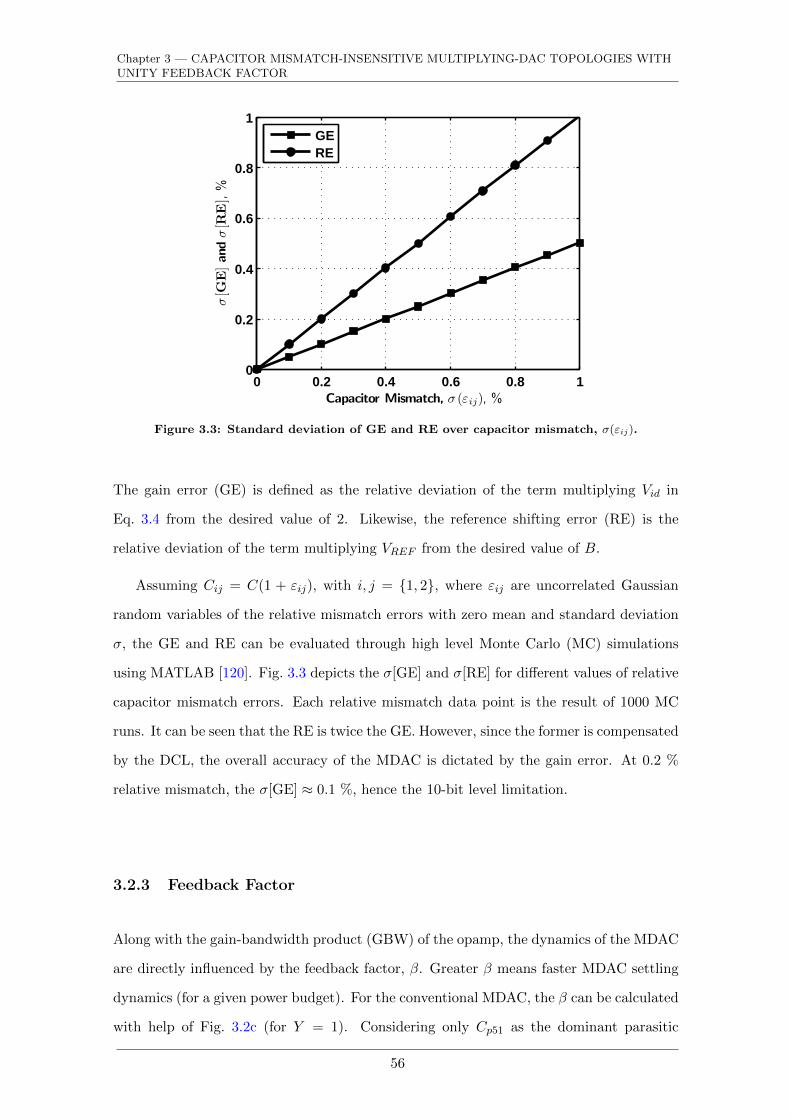
Chapter 3 — CAPACITOR MISMATCH-INSENSITIVE MULTIPLYING-DAC TOPOLOGIES WITHUNITY FEEDBACK FACTOR
0 0.2 0.4 0.6 0.8 10
0.2
0.4
0.6
0.8
1
σ[G
E]an
dσ[R
E],%
Capacitor Mismatch, σ (εij), %
GERE
Figure 3.3: Standard deviation of GE and RE over capacitor mismatch, σ(εij).
The gain error (GE) is defined as the relative deviation of the term multiplying Vid in
Eq. 3.4 from the desired value of 2. Likewise, the reference shifting error (RE) is the
relative deviation of the term multiplying VREF from the desired value of B.
Assuming Cij = C(1 + εij), with i, j = 1, 2, where εij are uncorrelated Gaussian
random variables of the relative mismatch errors with zero mean and standard deviation
σ, the GE and RE can be evaluated through high level Monte Carlo (MC) simulations
using MATLAB [120]. Fig. 3.3 depicts the σ[GE] and σ[RE] for different values of relative
capacitor mismatch errors. Each relative mismatch data point is the result of 1000 MC
runs. It can be seen that the RE is twice the GE. However, since the former is compensated
by the DCL, the overall accuracy of the MDAC is dictated by the gain error. At 0.2 %
relative mismatch, the σ[GE] ≈ 0.1 %, hence the 10-bit level limitation.
3.2.3 Feedback Factor
Along with the gain-bandwidth product (GBW) of the opamp, the dynamics of the MDAC
are directly influenced by the feedback factor, β. Greater β means faster MDAC settling
dynamics (for a given power budget). For the conventional MDAC, the β can be calculated
with help of Fig. 3.2c (for Y = 1). Considering only Cp51 as the dominant parasitic
56
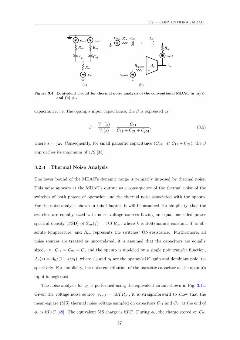
3.2 — CONVENTIONAL MDAC
vsw,1vsw,1
C21 C11
Ron
RonRon
vsw,1
(a)
vsw,2 C11C21
Ron
+voAv
Ron
vsw,2
vopamp
Ropamp
(b)
Figure 3.4: Equivalent circuit for thermal noise analysis of the conventional MDAC in (a) φ1
and (b) φ2.
capacitance, i.e. the opamp’s input capacitance, the β is expressed as
β =V −(s)
Vo(s)=
C11
C11 + C21 + Cp51, (3.5)
where s = jω. Consequently, for small parasitic capacitance (Cp51 C11 + C21), the β
approaches its maximum of 1/2 [33].
3.2.4 Thermal Noise Analysis
The lower bound of the MDAC’s dynamic range is primarily imposed by thermal noise.
This noise appears at the MDAC’s output as a consequence of the thermal noise of the
switches of both phases of operation and the thermal noise associated with the opamp.
For the noise analysis shown in this Chapter, it will be assumed, for simplicity, that the
switches are equally sized with noise voltage sources having an equal one-sided power
spectral density (PSD) of Ssw(f) = 4kTRon, where k is Boltzmann’s constant, T is ab-
solute temperature, and Ron represents the switches’ ON-resistance. Furthermore, all
noise sources are treated as uncorrelated, it is assumed that the capacitors are equally
sized, i.e., C11 = C21 = C, and the opamp is modeled by a single pole transfer function,
Av(s) = A0/(1 + s/p1), where A0 and p1 are the opamp’s DC gain and dominant pole, re-
spectively. For simplicity, the noise contribution of the parasitic capacitor at the opamp’s
input is neglected.
The noise analysis for φ1 is performed using the equivalent circuit shown in Fig. 3.4a.
Given the voltage noise source, vsw,1 = 4kTRon, it is straightforward to show that the
mean-square (MS) thermal noise voltage sampled on capacitors C11 and C21 at the end of
φ1 is kT/C [48]. The equivalent MS charge is kTC. During φ2, the charge stored on C21
57

Chapter 3 — CAPACITOR MISMATCH-INSENSITIVE MULTIPLYING-DAC TOPOLOGIES WITHUNITY FEEDBACK FACTOR
is completely transferred to C11. As a result, the MS output voltage is given by
v2osw,1 =kTC11 + kTC21
C211
=2kTC
C2=
2kT
C. (3.6)
However, as shown in Fig. 3.4b, other thermal noise sources, namely two switches and
the opamp, also contribute to the total output noise. The voltage noise source, vopamp,
represents the input-referred thermal noise of the opamp and has a PSD of Sopamp(f) =
4kTRopamp, where Ropamp is the opamp’s single-ended equivalent input-referred noise re-
sistance, which is dependent on opamp topology and sizing.
The transfer functions from the voltage noise sources, vsw,2, to the output can be
approximated by
Hsw,2(s) =vovsw,2
≈ C21
C11
1
1 + s/(βA0p1)=
1
1 + s/(βA0p1), (3.7)
assuming that βA0 1. Note that the C21/C11 term is only valid for the input switch.
The MS output thermal noise voltage produced by both switches in φ2 is given by
v2osw,2 = 2×∫ ∞0|Hsw,2(j2πf)|2Ssw,2(f)df =
2kTRon1/(βA0p1)
. (3.8)
Similarly, the TF of vopamp to the output is
Hopamp(s) =vo
vopamp≈ 1/β
1 + s/(βA0p1), (3.9)
and hence
v2oopamp =
∫ ∞0|Hopamp(j2πf)|2Sopamp(f)df =
kTRopamp(1/β)2
1/(βA0p1). (3.10)
Therefore, the total output MS thermal noise is
v2o = v2osw,1 + v2osw,2 + v2opamp = kT
[2
C+ βA0p1
(2Ron +
Ropampβ2
)]. (3.11)
For the fully differential conventional MDAC implementation, the total MS noise can
be written as
v2od = 2× kT[
2
C+ βA0p1
(2Ron +
Ropampβ2
)]. (3.12)
58

3.3 — CURRENT-MODE REFERENCE SHIFTING MDAC
The noise analysis of the conventional MDAC did not contemplate the noise contribution
of the reference voltage (VREF ) circuitry. As already mentioned in the previous chapter, if
these circuits are not adequately sized and decoupled, they will add noise to the MDAC’s
output, and can even be the ADC’s limiting factor [49].
3.3 Current-Mode Reference Shifting MDAC
This section proposes an MDAC circuit with unity feedback factor that is insensitive to
capacitor mismatch. Reference shifting occurs in current-mode during the amplification
phase. As an abbreviation this MDAC will be called CMRS-MDAC.
3.3.1 Principle of Operation
The proposed unity β, capacitor mismatch-insensitive 1.5-bit MDAC is shown in Fig. 3.5a.
Similarly to the conventional MDAC, this circuit operates in two clock phases. During φ1,
the differential input voltage is sampled on capacitors C1j , C2j , and C3j , j = 1, 2. During
φ2, capacitors C1j and C2j are associated in series around the opamp’s feedback loop and
the gain of two is obtained by voltage sum, instead of charge redistribution, as occurs
in the conventional implementation. Reference shifting occurs (during φ2) when current
sources, IP and IN , are turned on. These current sources sink/source current through the
series associated capacitors changing the output voltage by an amount proportional to the
respective current, feedback capacitance and duration of φ2. By the end of φ2 the output
voltage should have changed by an amount equal to ±VREF (differentially), for X and Z
modes. This situation is illustrated in Fig. 3.6, where the dashed lines indicate the flow
of current. Regarding the output waveforms, in Y operation mode it is exponential, but
for X and Z it has a ramped integrating characteristic until the end of φ2.
Following this approach for obtaining a capacitor mismatch-insensitive gain of two,
the circuit becomes sensitive to parasitic capacitors Cp2j and Cp3j (nodes between C2j
and C1j in Fig. 3.5). To attenuate this sensitivity, capacitors C3j are employed. Notice,
however, that these capacitors are shorted during φ2 because only the charge stored in
their parasitic capacitors (Cp6j) is used to compensate the charge stored on Cp2j and Cp3j ,
as shown next.
59

Chapter 3 — CAPACITOR MISMATCH-INSENSITIVE MULTIPLYING-DAC TOPOLOGIES WITHUNITY FEEDBACK FACTOR
VCM
VDD
Cp11
Cp21Cp31
Cp71
Cp41
C11C212
2
1
Vip11
Vin
2
C12C22
2
2
1 1
X*2 Y*2 Z*2
Z*2 Y*2 X*2
IN
IP1
1
Von
Vop- +
+ -
11
Cp51
1
2
11
Compensationcircuit
Cp61 Cp81
VCM
VCM
C32
C31
2
2
(a)
Cp21
Cp31
C21
C11
C31
Cp61
Vi VCM
(b)
C11C21
Cp21Cp31
Cp61
-
+
C31
Vo
v–
vx
VCM
(c)
Figure 3.5: (a) Fully differential enhanced feedback factor 1.5-bit mismatch-insensitiveMDAC with current-mode reference shifting. (b) Single-ended equivalent cir-cuit during sampling (φ1). (c) Single-ended equivalent circuit during φ2 for GEanalysis.
VDD
X Z
Z X
C11C21
C12C22
C31
C32
X+Z
X+Z
IP
IN
Vod+ -
- +VCM
Figure 3.6: Equivalent circuit to demonstrate the current-mode reference shifting. Situationdepicted for Z = 1.
3.3.2 Gain Error Analysis
The single-ended version of the MDAC (in Y mode) shown in Fig. 3.5c is used for the
GE analysis. The proposed MDAC’s TF is defined by charge conservation at nodes vx
and v−. Solving the charge conservation equations, the differential output voltage can be
60
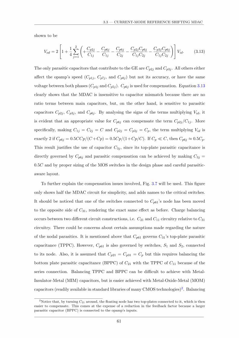
3.3 — CURRENT-MODE REFERENCE SHIFTING MDAC
shown to be
Vod = 2
1 +1
4
2∑j=1
(+Cp2jC1j
− Cp6jC1j
− Cp6jC2j
− Cp2jCp6jC1jC2j
− Cp3jCp6jC1jC2j
)Vid. (3.13)
The only parasitic capacitors that contribute to the GE are Cp2j and Cp3j . All others either
affect the opamp’s speed (Cp1j , Cp7j , and Cp8j) but not its accuracy, or have the same
voltage between both phases (Cp4j and Cp5j). Cp6j is used for compensation. Equation 3.13
clearly shows that the MDAC is insensitive to capacitor mismatch because there are no
ratio terms between main capacitors, but, on the other hand, is sensitive to parasitic
capacitors Cp2j , Cp3j , and Cp6j . By analysing the signs of the terms multiplying Vid, it
is evident that an appropriate value for Cp6j can compensate the term Cp2j/C1j . More
specifically, making C1j = C2j = C and Cp2j = Cp3j = Cp, the term multiplying Vid is
exactly 2 if Cp6j = 0.5CCp/(C+Cp) = 0.5Cp/(1+Cp/C). If Cp C, then Cp6j ≈ 0.5Cp.
This result justifies the use of capacitor C3j , since its top-plate parasitic capacitance is
directly governed by Cp6j and parasitic compensation can be achieved by making C3j =
0.5C and by proper sizing of the MOS switches in the design phase and careful parasitic-
aware layout.
To further explain the compensation issues involved, Fig. 3.7 will be used. This figure
only shows half the MDAC circuit for simplicity, and adds names to the critical switches.
It should be noticed that one of the switches connected to Cp61’s node has been moved
to the opposite side of C31, rendering the exact same effect as before. Charge balancing
occurs between two different circuit constructions, i.e. C21 and C11 circuitry relative to C31
circuitry. There could be concerns about certain assumptions made regarding the nature
of the nodal parasitics. It is mentioned above that Cp61 governs C31’s top-plate parasitic
capacitance (TPPC). However, Cp61 is also governed by switches, S1 and S2, connected
to its node. Also, it is assumed that Cp21 = Cp31 = Cp but this requires balancing the
bottom plate parasitic capacitance (BPPC) of C21 with the TPPC of C11 because of the
series connection. Balancing TPPC and BPPC can be difficult to achieve with Metal-
Insulator-Metal (MIM) capacitors, but is easier achieved with Metal-Oxide-Metal (MOM)
capacitors (readily available in standard libraries of many CMOS technologies)2. Balancing
2Notice that, by turning C21 around, the floating node has two top-plates connected to it, which is theneasier to compensate. This comes at the expense of a reduction in the feedback factor because a largerparasitic capacitor (BPPC) is connected to the opamp’s inputs.
61

Chapter 3 — CAPACITOR MISMATCH-INSENSITIVE MULTIPLYING-DAC TOPOLOGIES WITHUNITY FEEDBACK FACTOR
Cp21Cp31
C212
2
1
Vip11
22
1
Vop
11
Cp61
VCM
C31S1
S2
S3
S5
- +
S4
C11
Figure 3.7: Compensation circuit close-up and parasitic capacitor analysis.
Table 3.1: Parasitic capacitor governance and balancing using Metal-Insulator-Metal (MIM)capacitors and Metal-Oxide-Metal (MOM) capacitors. Capacitor sizes defined byC11 = C21 = 2C31 = C and nominal switch size defined by W/L, where W and L arethe width and length of the switch’s channel, respectively. Note that, the switchcontributes a parasitic capacitance to each node it is connected to: Cgs to onenode and Cgd to the other, where Cgs = Cgd = 0.5WLCox.
ParasiticGoverned by Balance
Capacitor
using MIM capacitors
Cp21 S3, S4, TPPCC11 C × TPPCC + 0.5WLCox + 0.5WLCox = C × TPPCC +WLCox
Cp31 S3, S5, BPPCC21 C × BPPCC + 0.5WLCox + 0.5WLCox = C × BPPCC +WLCox
Cp61 S1, S2, TPPCC31C2× TPPCC + 0.5W
2LCox + 0.5W
2LCox = C×TPPCC+WLCox
2
using MOM capacitors
Cp21 S3, S4, PPCC11 C × PPCC + 0.5WLCox + 0.5WLCox = C × PPCC +WLCox
Cp31 S3, S5, PPCC21 C × PPCC + 0.5WLCox + 0.5WLCox = C × PPCC +WLCox
Cp61 S1, S2, PPCC31C2× PPCC + 0.5W
2LCox + 0.5W
2LCox = C×PPCC+WLCox
2
PPC - plate parasitic capacitance; TPPC - top PPC; BPPC - bottom PPC
switches can be achieved by making S1 and S2 half of S4,5 and S3, respectively. Table 3.1
summarizes the effect and balancing of the crucial parasitic capacitors and demonstrates
that Cp61 = Cp21,31/2 can be achieved by using MOM capacitors, and careful design and
layout (refer to Fig. 3.7 for component names). If MIM capacitors are employed, Cp31 will
not be compensated as desired. However, referring to Eq. 3.13, Cp31 has a second order
effect on the gain error and therefore, can be neglected.
The statistical analysis of the GE can be achieved by referring back to Eq. 3.13 and by
defining Cij = C(1 + εij) and C3j = 0.5C(1 + εij), with i, j = 1, 2, Cpij = Cp(1 + εpij)
and Cp6j = 0.5Cp(1 + εp6j)/(1 + α), with i = 2, 3 and j = 1, 2, where εij and εpij are
uncorrelated Gaussian random variables of the relative errors with zero mean and standard
deviation σ, and α = Cp/C. Monte Carlo simulations using MATLAB and Spectre are
employed to evaluate the obtained expression. The standard deviation plus the absolute
62
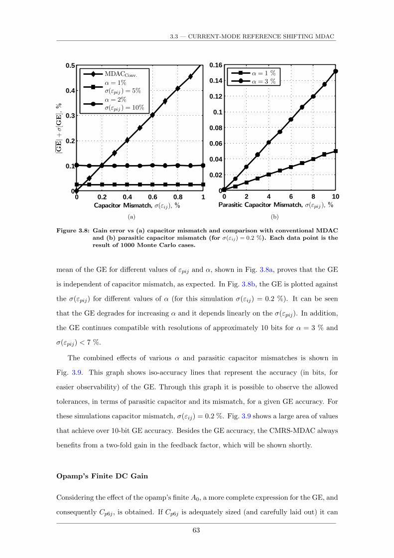
3.3 — CURRENT-MODE REFERENCE SHIFTING MDAC
0 0.2 0.4 0.6 0.8 10
0.1
0.2
0.3
0.4
0.5|G
E|+
σ[G
E],%
Capacitor Mismatch, σ(εij), %
MDACConv.
α = 1%σ(εpij ) = 5%
α = 2%σ(εpij ) = 10%
(a)
0 2 4 6 8 100
0.02
0.04
0.06
0.08
0.1
0.12
0.14
0.16
Parasitic Capacitor Mismatch, σ(εpij ), %
α = 1 %α = 3 %
(b)
Figure 3.8: Gain error vs (a) capacitor mismatch and comparison with conventional MDACand (b) parasitic capacitor mismatch (for σ(εij) = 0.2 %). Each data point is theresult of 1000 Monte Carlo cases.
mean of the GE for different values of εpij and α, shown in Fig. 3.8a, proves that the GE
is independent of capacitor mismatch, as expected. In Fig. 3.8b, the GE is plotted against
the σ(εpij) for different values of α (for this simulation σ(εij) = 0.2 %). It can be seen
that the GE degrades for increasing α and it depends linearly on the σ(εpij). In addition,
the GE continues compatible with resolutions of approximately 10 bits for α = 3 % and
σ(εpij) < 7 %.
The combined effects of various α and parasitic capacitor mismatches is shown in
Fig. 3.9. This graph shows iso-accuracy lines that represent the accuracy (in bits, for
easier observability) of the GE. Through this graph it is possible to observe the allowed
tolerances, in terms of parasitic capacitor and its mismatch, for a given GE accuracy. For
these simulations capacitor mismatch, σ(εij) = 0.2 %. Fig. 3.9 shows a large area of values
that achieve over 10-bit GE accuracy. Besides the GE accuracy, the CMRS-MDAC always
benefits from a two-fold gain in the feedback factor, which will be shown shortly.
Opamp’s Finite DC Gain
Considering the effect of the opamp’s finite A0, a more complete expression for the GE, and
consequently Cp6j , is obtained. If Cp6j is adequately sized (and carefully laid out) it can
63
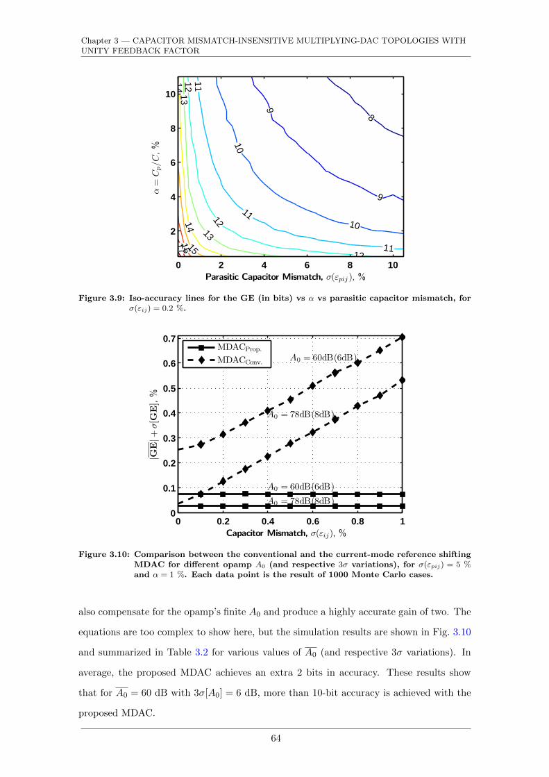
Chapter 3 — CAPACITOR MISMATCH-INSENSITIVE MULTIPLYING-DAC TOPOLOGIES WITHUNITY FEEDBACK FACTOR
8
9
9
10
10
11
11
11
12
12
12
13
13
1414
151617
α=
Cp/C,%
Parasitic Capacitor Mismatch, σ(εpij ), %0 2 4 6 8 10
2
4
6
8
10
Figure 3.9: Iso-accuracy lines for the GE (in bits) vs α vs parasitic capacitor mismatch, forσ(εij) = 0.2 %.
0 0.2 0.4 0.6 0.8 10
0.1
0.2
0.3
0.4
0.5
0.6
0.7
A0 = 60dB(6dB)
A0 = 78dB(8dB)
A0 = 60dB(6dB)
A0 = 78dB(8dB)
|GE|+
σ[G
E],%
Capacitor Mismatch, σ(εij), %
MDACProp.
MDACConv.
Figure 3.10: Comparison between the conventional and the current-mode reference shiftingMDAC for different opamp A0 (and respective 3σ variations), for σ(εpij) = 5 %and α = 1 %. Each data point is the result of 1000 Monte Carlo cases.
also compensate for the opamp’s finite A0 and produce a highly accurate gain of two. The
equations are too complex to show here, but the simulation results are shown in Fig. 3.10
and summarized in Table 3.2 for various values of A0 (and respective 3σ variations). In
average, the proposed MDAC achieves an extra 2 bits in accuracy. These results show
that for A0 = 60 dB with 3σ[A0] = 6 dB, more than 10-bit accuracy is achieved with the
proposed MDAC.
64

3.3 — CURRENT-MODE REFERENCE SHIFTING MDAC
Table 3.2: Gain error (%) versus opamp’s A0 and 3σ variations (dB).(σ(εij) = 0.2 %, σ(εpij) = 5 %, and α = 1 %)
A0 (3σ[A0]) 40 (5) 50 (6) 60 (6) 70 (8) 80 (8) 90 (10)
GECMRS 0.59 0.23 0.076 0.04 0.026 0.025
GEConventional 2.4 0.83 0.32 0.17 0.12 0.11
Charge Injection and Clock Feed-through
Regarding the effects of charge injection and clock feed-through on the compensation
circuit, simulations show that these result in an offset term, as shown in
Vod =2
1 +1
4
2∑j=1
(+Cp2jC1j
− Cp6jC1j
− Cp6jC2j
− Cp2jCp6jC1jC2j
− Cp3jCp6jC1jC2j
)Vid+ qinj1
(C11 + C21 + Cp21 + Cp31
C11C21
)− qinj2
(C12 + C22 + Cp22 + Cp32
C12C22
),
(3.14)
where qinj1 and qinj2 represent the charge injection and clock feed-through of the positive
and negative paths of the MDAC3. As can be seen neither nonideal effects affect the GE,
given that the offset term is signal independent. The effect of charge injection is min-
imized with signal independent sampling which is assumed for these simulations, hence
the offset term being signal independent. Nevertheless, VCM (common-mode voltage or
analog ground) dependent sampling occurs, which adds an offset to the output voltage.
However, by using a fully differential design, the VCM dependent charge injection will can-
cel at the differential output. Clock feed-through is attenuated by using dummy switches
and, again, a fully differential design. Nevertheless, careful layout practice is important
to minimize parasitic couplings and guarantee differential design. Fig. 3.11a shows the
offset for various values of charge injection and clock feed-through mismatch. This offset
measures the mismatch between the charge injected in the two differential signal paths.
For the simulation, capacitor and parasitic capacitor mismatch are considered.
VCM Mismatch
By comparing Fig. 3.1 with Fig. 3.5a it can be noticed that VCM , for the CMRS-MDAC
is injected at two different nodes. The VCM mismatch between these two nodes does not
3Charge injection is given by qinj = −0.5WLCox(VG−VT ) + 0.5WLCoxVS , where the VS term is signaldependent. It is assumed that half the charge is injected into each node. Clock feed-through injectedvoltage is given by VGCovW/(CovW + C).
65

Chapter 3 — CAPACITOR MISMATCH-INSENSITIVE MULTIPLYING-DAC TOPOLOGIES WITHUNITY FEEDBACK FACTOR
0 2 4 6 8 100
0.5
1
1.5
2
2.5
3Offset,
mV
Charge Mismatch, σ(εq), %
(a)
10−1
100
101
102
−30
−25
−20
−15
−10
−5
0
5
Offset,
µV
VCM Mismatch, σ(εVCM), %
(b)
Figure 3.11: Differential output offset due to: (a) Charge injection and clock feed-throughmismatch and (b) VCM mismatch. Simulation conditions for the capacitors:σC(εij) = 0.2 %, σp(εpij) = 5 %, and α = 1 %. For the switches: W/L = 10/0.12, gatevoltage VG = 1.2 V, threshold voltage VT = 0.4 V, normalized gate oxide capaci-tance Cox = 12.6 fF/µm2, and normalized overlap capacitance, Cov = 0.3 fF/µm.Each data point is the result of 1000 Monte Carlo cases.
affect the accuracy of the gain of two. However, it does add an offset term to the MDAC’s
output voltage which can be minimized with fully differential design and careful VCM path
layout. Fig. 3.11b shows the offset for various values of mismatch between the sampled
VCM of the two signal paths that should, under ideal conditions, cancel at the differential
output. For the simulation, capacitor and parasitic capacitor mismatch are considered.
As can be seen, for mismatches up to 100 %, the offset is negligible.
3.3.3 Reference Shifting Error Analysis
For the RE analysis, the circuit of Fig. 3.12 will be used. With X = 1, as an example,
the current source IN is connected to the inverting input of the opamp, while IP is con-
nected to the noninverting input. To simplify the circuit analysis, it will be assumed that
the total current Ik, k = P,N flows through the feedback path formed by the series
associated capacitors C2j and C1j , j = 1, 2, and the two switches that close the loop.
This assumption is based on the fact that the remaining parasitic paths have much higher
impedance and thus only a very small fraction of the current will flow through these paths.
A fully differential analysis will be carried out for the RE, by defining IP = IN = IREF /2,
66

3.3 — CURRENT-MODE REFERENCE SHIFTING MDAC
Vp
Vn
IN
IP
VDDC11C21
X=1 Z=0
Z=0 X=1
C12C22
R1
R2
Vop
Von
- +
+ -
Figure 3.12: MDAC configuration with current-mode reference shifting active for X = 1.Circuit used for RE analysis.
R1 = R2 = 2Ron, Cj = C1jC2j/(C1j + C2j), j = 1, 24. Defining the opamp’s input
nodes’ voltages, Vp and Vn, as
Vp = Vop − (R1 + 1/sC1)IREF /2
Vn = Von + (R2 + 1/sC2)IREF /2,
(3.15)
and substituting them into Vod = −Av(Vp − Vn), solving for Vod, and applying the single
pole TF of Av, we obtain
Vod(s) =1
2(1 + s/A0p1)
(R1 +R2 +
1
sC1+
1
sC2
)IREF . (3.16)
Considering a step function IREF (s) = IREF /s, Vod(t) is obtained applying the inverse
Laplace transform,
Vod(t) =IREF
2
2∑i=1
1
Ci
[t+
(e−GBWt − 1)(1−GBWRiCi)
GBW
], (3.17)
where GBW = A0p1. Assuming GBW 1/(RiCi) and integration (or reference shifting)
time Ti = 1/(2FS), we can simplify Eq. 3.17 to
Vod(Ti) ∼=IREF
2
(Ti +
e−GBWTi − 1
GBW
)(C11 + C21
C11C21+C12 + C22
C12C22
). (3.18)
4If IP and IN are not exactly matched, a current error (Ie) is introduced and results in an additiveterm appearing at the end of Eq. 3.18. It only affects the capacitor mismatch error (Eq. 3.20), dependingmainly on an Ie/IREF term. Simulation results show that, for values of Ie/IREF up to 20 %, this errormay be neglected.
67

Chapter 3 — CAPACITOR MISMATCH-INSENSITIVE MULTIPLYING-DAC TOPOLOGIES WITHUNITY FEEDBACK FACTOR
From Eq. 3.18 three sources of error emerge: opamp’s dynamic limitation given by GBW,
capacitor mismatch (ratio terms between capacitors) and integration time variations rep-
resented by Ti. These three sources of error are analysed next.
Opamp’s Dynamic Limitation
Assuming C11 = C21 = C12 = C22 = C and a fixed Ti, the error due to GBW is given by
εGBW =Vod − Vodideal
Vodideal
∼= −1
GBWTi, (3.19)
where Vodideal = 2IREFTi/C. As an example, a 12-bit application needs N ln(2) ≈ 9 time
constants for linear settling. Therefore, the closed-loop GBW = 9 × 2FS = 9/Ti in units
of rad/s. Substituting in Eq. 3.19 leads to an absolute error of 11 %. Although large, a
small increase in IREF compensates for this GBW limitation.
This compensation is demonstrated in Fig. 3.13. This graph combines various values
of GBW and IREF , including capacitor mismatch, with the final result being Eq. 3.18
(it is considered Vod = VREF ). The conditions for the simulations of this hypothetical
case are: C = 1 pF, nominal GBW = 3.2 GHz, Ti = 420 ps, which yields a nominal
IREF = 600 µA. For capacitor mismatch it is considered σ(εij) = 0.2 %. The objective is
to achieve VREF = 0.5 V. Fig. 3.13 has two reference lines (dotted lines). The horizontal
reference line for IREF = 600 µA shows that it is very difficult to obtain VREF = 0.5 V
for practical values of GBW. On the other hand, the vertical reference line, for GBW
= 3.2 GHz, shows that by increasing IREF from 600 to 684 µA, VREF = 0.5 V is achieved.
This corresponds to an increase of 14 % in the reference current. Therefore, a small
increase in the reference current compensates for limited GBW.
Capacitor Mismatch
Assuming GBW →∞ and a fixed Ti, the resulting error is given by
εC =Vod − Vodideal
Vodideal=C
4
(C11 + C21
C11C21+C12 + C22
C12C22
)− 1. (3.20)
If Cij = C(1 + εij), where εij are assumed uncorrelated Gaussian random variables with
zero mean and standard deviation σ, and assuming σ sufficiently small, such that 1/(1 +
68

3.3 — CURRENT-MODE REFERENCE SHIFTING MDAC
0.30.35
0.4
0.4
0.45
0.45
0.5
0.5
0.55
0.55
0.6
I REF,µA
GBW, GHz3.2 5 10 15 20
500
550
600
650
684700
Figure 3.13: Iso-VREF lines vs GBW vs IREF . Error due to finite GBW and compensationby increasing IREF .
εij) ≈ 1 − εij , we obtain σεC = σC/2 = 0.1 % (assuming σC = 0.2 %). Therefore, this
error is easily corrected by the digital correction logic.
Integration Time Variation
Assuming GBW→∞, all capacitors are equal, and an integration time given by Ti(1+εTi),
where εTi represents the deviation from the ideal integration time, the resulting integration
time error is
εT =Vod − Vodideal
Vodideal=Ti(1 + εTi)− Ti
Ti= εTi . (3.21)
This means that this error is dependent on the jitter noise of the system the MDAC is
embedded in. Therefore, comparing all error sources, this represents the smallest one,
which are dominated by the finite GBW of the opamp.
A final TF expression for the CMRS-MDAC can be obtained by summing Eq. 3.13
with B times Eq. 3.18 (B represents the MDAC operation mode), which is given by
Vod =2
1 +1
4
2∑j=1
(+Cp2jC1j
− Cp6jC1j
− Cp6jC2j
− Cp2jCp6jC1jC2j
− Cp3jCp6jC1jC2j
)Vid+B × 1
2
(Ti +
e−GBWTi − 1
GBW
)(C11 + C21
C11C21+C12 + C22
C12C22
)IREF .
(3.22)
69

Chapter 3 — CAPACITOR MISMATCH-INSENSITIVE MULTIPLYING-DAC TOPOLOGIES WITHUNITY FEEDBACK FACTOR
0 0.2 0.4 0.6 0.8 10
0.1
0.2
0.3
0.4
0.5
50 ps 125 ps
417 ps 1043 ps
Time, ns
Differen
tial
Outpu
tVoltage
,Vod,V
VodMDACCMRS
VodMDACConv.
τCLMDACCMRS
τCLMDACConv.
TS12−bitMDACCMRS
TS12−bitMDACConv.
Figure 3.14: Step response comparison between conventional MDAC and CMRS-MDAC,illustrating the effect of the β enhancement.
3.3.4 Feedback Factor
The β of the CMRS-MDAC can be derived with the help of Fig. 3.5c considering Cp71
(i.e., the opamp’s input parasitic capacitance, see Fig. 3.5a) as the dominant parasitic
capacitor, which results
βY =V −(s)
Vo(s)=
1
1 + Cp71C11+C21C11C21
. (3.23)
If Cp71 C11C21/(C11 + C11), the feedback factor approximates unity. Therefore, the
resulting β is two times greater than that of the conventional MDAC, which is clearly a
relevant advantage since the speed/power ratio doubles. The enhanced β also reduces the
effective load, CLeff = CL + (1 − β)Cfeedback (Cfeedback is the equivalent series feedback
capacitance), therefore the total gain is approximately 2.5 times over the conventional
MDAC5. This can be seen in the simulation results of Fig. 3.14, where the closed-loop
time constant and 12-bit settling time of the conventional MDAC are 2.5 times that of the
proposed MDAC. For these simulations the following conditions are considered: the model
of the opamp has A0 = 106 dB, GBW = 3.2 GHz, and a load capacitance, CL = 2 pF.
Eq. 3.23 refers to the feedback factor for Y operation mode. In X and Z modes,
considering a finite output impedance of the current source (an RS in parallel with a CS),
5This is true when comparing both the conventional and CMRS-MDACs with an equal load capaci-tor, CL. However, in a pipeline (or similar) ADC, employing the CMRS-MDAC in all its stages, the βenhancement reduces to 2, because of the extra sampling half-capacitor, C3j , which loads each stage.
70
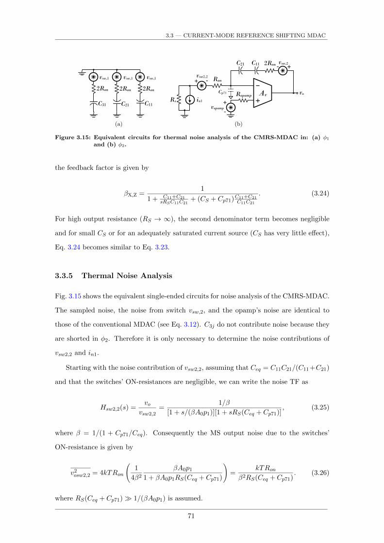
3.3 — CURRENT-MODE REFERENCE SHIFTING MDAC
C31 C21 C11
2Ron
vsw,1 vsw,1 vsw,1
2Ron 2Ron
(a)
Ronvsw2,2
Cp71
+ -
in1Rsvopamp
C11C21 2Ron
+vo
+
-
Av
+-vsw,2
Ropamp
(b)
Figure 3.15: Equivalent circuits for thermal noise analysis of the CMRS-MDAC in: (a) φ1
and (b) φ2.
the feedback factor is given by
βX,Z =1
1 + C11+C21sRSC11C21
+ (CS + Cp71)C11+C21C11C21
. (3.24)
For high output resistance (RS → ∞), the second denominator term becomes negligible
and for small CS or for an adequately saturated current source (CS has very little effect),
Eq. 3.24 becomes similar to Eq. 3.23.
3.3.5 Thermal Noise Analysis
Fig. 3.15 shows the equivalent single-ended circuits for noise analysis of the CMRS-MDAC.
The sampled noise, the noise from switch vsw,2, and the opamp’s noise are identical to
those of the conventional MDAC (see Eq. 3.12). C3j do not contribute noise because they
are shorted in φ2. Therefore it is only necessary to determine the noise contributions of
vsw2,2 and in1.
Starting with the noise contribution of vsw2,2, assuming that Ceq = C11C21/(C11+C21)
and that the switches’ ON-resistances are negligible, we can write the noise TF as
Hsw2,2(s) =vo
vsw2,2=
1/β
[1 + s/(βA0p1)][1 + sRS(Ceq + Cp71)], (3.25)
where β = 1/(1 + Cp71/Ceq). Consequently the MS output noise due to the switches’
ON-resistance is given by
v2osw2,2 = 4kTRon
(1
4β2βA0p1
1 + βA0p1RS(Ceq + Cp71)
)=
kTRonβ2RS(Ceq + Cp71)
. (3.26)
where RS(Ceq + Cp71) 1/(βA0p1) is assumed.
71

Chapter 3 — CAPACITOR MISMATCH-INSENSITIVE MULTIPLYING-DAC TOPOLOGIES WITHUNITY FEEDBACK FACTOR
The TF of the last noise source, in1, is given by
Hin1(s) =voin1
=Av
(Av + 1)sCeq=
1
(1 + s/(A0p1))sCeq. (3.27)
In the derivation of Eq. 3.27 it is assumed that all noise current flows through the feedback
path and that A0 1. We note that this TF has a pole at zero, which resembles
an integrating characteristic, and thus, the noise PSD integral is unbounded at the low
frequency limit. Therefore, the method used until now to compute the output noise can not
be directly applied6[121]. An alternative method uses a rectangular window, w(t), from 0
to Ti (integration time), to shape the impulse response hin1(t), i.e., hin1w(t) = hin1(t)w(t),
and then applies the traditional method with the TF Hin1w [121]. The impulse response
obtained from Eq. 3.27 is
hin1(t) =1− e−A0p1t
Ceq. (3.28)
Applying a rectangular window function, we have
hin1w(t) = hin1(t)w(t) = hin1(t)[u(t)− u(t− Ti)], (3.29)
where u(t) is the unit step function. By determining the Fourier transform of Eq. 3.29
and knowing that the PSD of the noise current is Sin1(f) = 4γkTgm (where γ and gm are
the transistor’s excess noise factor and transconductance, respectively), the contribution
to the output noise can be calculated as
v2oin1 =
∫ ∞0|Hin1w(j2πf)|2Sin1(f)df = 4γkTgm
(−3 + 2a+ 4e−a − e−2a
4C2eqA0p1
), (3.30)
where a = A0p1Ti = GBWTi. For GBW 1/Ti, Eq. 3.30 can be simplified to
v2oin1 =2γkTgmTi
C2eq
. (3.31)
Considering the fully differential implementation of the CMRS-MDAC and by adding all
noise contributions given by Eq. 3.12,3.26,3.31, we finally arrive at the expression of the
6The method used until now is based on the formula∫∞
0|H(j2πf)|2S(f) df .
72
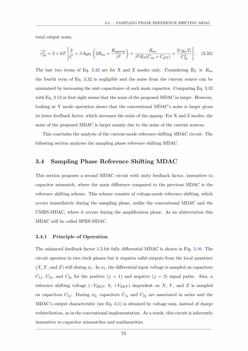
3.4 — SAMPLING PHASE REFERENCE SHIFTING MDAC
total output noise,
v2od = 2× kT[
2
C+ βA0p1
(2Ron +
Ropampβ2
)+
Ronβ2RS(Ceq + Cp71)
+2γgmTiC2eq
]. (3.32)
The last two terms of Eq. 3.32 are for X and Z modes only. Considering RS Ron
the fourth term of Eq. 3.32 is negligible and the noise from the current source can be
minimized by increasing the unit capacitance of each main capacitor. Comparing Eq. 3.32
with Eq. 3.12 at first sight seems that the noise of the proposed MDAC in larger. However,
looking at Y mode operation shows that the conventional MDAC’s noise is larger given
its lower feedback factor, which increases the noise of the opamp. For X and Z modes, the
noise of the proposed MDAC is larger mainly due to the noise of the current sources.
This concludes the analysis of the current-mode reference shifting MDAC circuit. The
following section analyses the sampling phase reference shifting MDAC.
3.4 Sampling Phase Reference Shifting MDAC
This section proposes a second MDAC circuit with unity feedback factor, insensitive to
capacitor mismatch, where the main difference compared to the previous MDAC is the
reference shifting scheme. This scheme consists of voltage-mode reference shifting, which
occurs immediately during the sampling phase, unlike the conventional MDAC and the
CMRS-MDAC, where it occurs during the amplification phase. As an abbreviation this
MDAC will be called SPRS-MDAC.
3.4.1 Principle of Operation
The enhanced feedback factor 1.5-bit fully differential MDAC is shown in Fig. 3.16. The
circuit operates in two clock phases but it requires valid outputs from the local quantizer
(X, Y , and Z) still during φ1. In φ1, the differential input voltage is sampled on capacitors
C1j , C2j , and C3j for the positive (j = 1) and negative (j = 2) signal paths. Also, a
reference shifting voltage (−VREF , 0, +VREF ) dependent on X, Y , and Z is sampled
on capacitors C1j . During φ2, capacitors C1j and C2j are associated in series and the
MDAC’s output characteristic (see Eq. 3.1) is obtained by voltage sum, instead of charge
redistribution, as in the conventional implementation. As a result, this circuit is inherently
insensitive to capacitor mismatches and nonlinearities.
73

Chapter 3 — CAPACITOR MISMATCH-INSENSITIVE MULTIPLYING-DAC TOPOLOGIES WITHUNITY FEEDBACK FACTOR
Cp11
Cp21Cp31
Cp71
Cp41
C11C212
2
1
Vip11
Vin
2
C12C22
2
2
1 1
Von
Vop- +
+ -
11
Cp51
1
2
11
Compensationcircuit
Cp61 Cp81
Y*1 Z*1X*1
+VREF -VREFVCM
Y*1 X*1Z*1
+VREF -VREFVCM
VCM
VCM
C31
C32
2
2
(a)
VCM
Cp21C21
C11
C31
Vi
-VREFX
Y
ZVCM
+VREF
Cp61
Cp31
(b)
C11C21
Cp21Cp31
Cp61
-
+
C31
Vo
v–
vx
VCM
(c)
Figure 3.16: (a) Enhanced feedback factor, fully differential 1.5-bit mismatch-insensitiveMDAC with sampling phase reference shifting. (b) Single-ended equivalentcircuit during sampling (φ1). (c) Single-ended equivalent circuit during φ2 forGE analysis.
Like the previous MDAC, this approach for obtaining a capacitor mismatch-insensitive
gain of two causes the circuit to become sensitive to parasitic capacitors Cp2j and Cp3j
(nodes between C2j and C1j). To attenuate this sensitivity, capacitors C3j are employed.
Notice, however, that these capacitors are shorted during φ2 because only the charge
stored in their parasitic capacitors (Cp6j) is used to compensate the charge stored on Cp2j
and Cp3j . The compensation circuit is shown in the shaded area of Fig. 3.16a.
This MDAC is capable of achieving a feedback factor of one, is insensitive to capacitor
mismatch, and still uses voltage-mode reference shifting. All these benefits are accompa-
nied by some penalties, namely the opamp’s dynamics. As mentioned above, this MDAC
needs the local quantizer’s decision during φ1, which means that the local quantizer has
half the sampling period to make a decision. After that decision is made, in case it is X or
Z, ±VREF has to be switched in at C11’s top-plate. This switching causes a disturbance of
74
3.4 — SAMPLING PHASE REFERENCE SHIFTING MDAC
the sampling, and as a result, the dynamics of the MDAC changes and the opamp needs
to re-settle. To avoid prolonged settling (after ±VREF has been switched in), the speed of
the opamp has to be higher.
To demonstrate that the GBW of this opamp (for correct settling) is not higher than
that of the conventional MDAC, consider the following. The GBW of an opamp sized for
the conventional MDAC is given by
GBW =1
τβ, τ =
Tsettlingn
(3.33)
where Tsettling = TS/2 = 1/(2FS) is the available time for opamp settling and n is the
number of necessary time constants that guarantees a certain settling accuracy, given
by n = N ln(2), where N is the desired accuracy. As already shown, the βConv. of the
conventional opamp is 1/2. Simplifying Eq. 3.33 results in
GBW =2N ln(2)
TSβConv.= 4N ln(2)FS (3.34)
The GBW of an opamp sized for the SPRS-MDAC, where βProp. = 1 and only a quarter
of TS is available for settling, is given by
GBW =4N ln(2)
TSβProp.= 4N ln(2)FS (3.35)
As can be seen by comparing Eq. 3.35 and Eq. 3.34, the same result is rendered. There-
fore, the opamps for each MDAC will have the same GBW. To conclude this analysis,
although the feedback factor enhancement does not translate into higher power efficiency,
this MDAC still benefits from its insensitivity to capacitor mismatch, as already demon-
strated.
3.4.2 Gain Error Analysis
Detailed gain error analysis for this MDAC in Y mode has already been carried out in the
gain error analysis subsection of the previous MDAC (Section 3.3.2), and therefore, will
not be repeated here.
75

Chapter 3 — CAPACITOR MISMATCH-INSENSITIVE MULTIPLYING-DAC TOPOLOGIES WITHUNITY FEEDBACK FACTOR
3.4.3 Reference Shifting Error Analysis
This MDAC’s TF is defined by charge conservation at nodes vx and v−, similar to the
previous MDAC. Solving the charge conservation equations, the differential output voltage
with reference shifting is given by
Vod =2
1 +1
4
2∑j=1
(+Cp2jC1j
− Cp6jC1j
− Cp6jC2j
− Cp2jCp6jC1jC2j
− Cp3jCp6jC1jC2j
)Vid+
1 +1
2
2∑j=1
Cp2jC1j
B · VREF ,(3.36)
where VREF represents the differential reference voltage. As can be seen from Eq. 3.36 the
term multiplying Vid is the same as that shown in Eq. 3.13, while the term multiplying
VREF represents the reference shifting term, which should ideally be one. Therefore, the
reference shifting error is given by 1/22∑j=1
Cp2j/C1j , which is of the order Cp/C, thus is
not of great concern since it can be corrected by the digital correction logic.
Charge Injection and Clock Feed-through
The effects of charge injection and clock feed-through are more pronounced in this MDAC
due to the VREF sampling. Sampling capacitors C1j , j = 1, 2, depending on the MDAC’s
operation mode, may sample±VREF in one signal path, while the other signal path samples
∓VREF . This means that the injected charge will not cancel at the differential output,
even under ideal conditions. Rewriting the charge conservation equations considering
VREF charge injection and clock feed-through, the MDAC’s TF becomes
Vod =2
1 +1
4
2∑j=1
(+Cp2jC1j
− Cp6jC1j
− Cp6jC2j
− Cp2jCp6jC1jC2j
− Cp3jCp6jC1jC2j
)Vid+
1 +1
2
2∑j=1
Cp2jC1j
B · VREF+ qinj1
(C11 + C21 + Cp21 + Cp31
C11C21
)− qinj2
(C12 + C22 + Cp22 + Cp32
C12C22
)+qvref+C11
− qvref−C12
,
(3.37)
where the first line represents the gain of two, the second line is the reference shifting
term, the third line represents the charge injection (gate voltage term) and clock feed-
through, and finally, the last line shows the charge injected due to the different sampled
76

3.4 — SAMPLING PHASE REFERENCE SHIFTING MDAC
0 2 4 6 8 108
9
10
11
12
13
Offset,
mV
VREF Charge Mismatch, σ(εq), %
Figure 3.17: Differential output offset due to VREF charge injection and clock feed-throughmismatch. Simulation conditions for the capacitors: σC(εij) = 0.2 %, σp(εpij) =5 %, and α = 1 %. For the switches: W/L = 10/0.12, gate voltage VG = 1.2 V,threshold voltage VT = 0.4 V, differential VREF = 0.5 V, normalized gateoxide capacitance Cox = 12.6 fF/µm2, and normalized overlap capacitance,Cov = 0.3 fF/µm. Each data point is the result of 1000 Monte Carlo cases.
reference voltages (source voltage term). As should be noticed, the reference shifting
error also contributes to the total offset, which is the largest offset contributor. The total
offset is shown in Fig. 3.17 for various values of charge injection and clock feed-through
mismatch. Capacitor and parasitic capacitor mismatch are also considered. As can be
seen in Fig. 3.17, even for matched charge injection, the offset error is around 9 mV (a
normalized full-scale input of 1 Vpp is assumed). Nevertheless, this error can still be
corrected by the DCL.
3.4.4 Feedback Factor
The feedback factor analysis is identical to the previous MDAC circuit and the β expression
is described by Eq. 3.23 (see Section 3.3.4). As mentioned before, neglecting parasitics, it
is nominally equal to 1.
3.4.5 Thermal Noise Analysis
For the thermal noise analysis of this MDAC, the equivalent circuits shown in Fig. 3.18
are used. Excluding C3j , j = 1, 2 from the analysis, given that it is shorted during
φ2, the noise analysis becomes identical to the one carried for the conventional MDAC
77
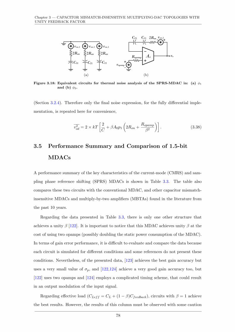
Chapter 3 — CAPACITOR MISMATCH-INSENSITIVE MULTIPLYING-DAC TOPOLOGIES WITHUNITY FEEDBACK FACTOR
C31 C21 C11
2Ron
vsw,1 vsw,1 vsw,1
2Ron 2Ron
(a)
vopamp
C11C21 2Ron
+vo
+
-
Av
+-vsw,2
Ropamp
(b)
Figure 3.18: Equivalent circuits for thermal noise analysis of the SPRS-MDAC in: (a) φ1
and (b) φ2.
(Section 3.2.4). Therefore only the final noise expression, for the fully differential imple-
mentation, is repeated here for convenience,
v2od = 2× kT[
2
C+ βA0p1
(2Ron +
Ropampβ2
)]. (3.38)
3.5 Performance Summary and Comparison of 1.5-bit
MDACs
A performance summary of the key characteristics of the current-mode (CMRS) and sam-
pling phase reference shifting (SPRS) MDACs is shown in Table 3.3. The table also
compares these two circuits with the conventional MDAC, and other capacitor mismatch-
insensitive MDACs and multiply-by-two amplifiers (MBTAs) found in the literature from
the past 10 years.
Regarding the data presented in Table 3.3, there is only one other structure that
achieves a unity β [122]. It is important to notice that this MDAC achieves unity β at the
cost of using two opamps (possibly doubling the static power consumption of the MDAC).
In terms of gain error performance, it is difficult to evaluate and compare the data because
each circuit is simulated for different conditions and some references do not present these
conditions. Nevertheless, of the presented data, [123] achieves the best gain accuracy but
uses a very small value of σp, and [122,124] achieve a very good gain accuracy too, but
[122] uses two opamps and [124] employs a complicated timing scheme, that could result
in an output modulation of the input signal.
Regarding effective load (CLeff = CL + (1− β)Cfeedback), circuits with β = 1 achieve
the best results. However, the results of this column must be observed with some caution
78

3.5 — PERFORMANCE SUMMARY AND COMPARISON OF 1.5-BIT MDACS
when considering a pipeline (or similar) ADC architecture, where all stages use the same
circuit structure. In this situation, CL is substituted by the respective values of the
‘Input Sampling Capacitance’ column. Using as an example the conventional and proposed
MDACs, the effective load of the conventional MDAC (if it is employed in all stages of a
pipeline converter) is 2.5C which is the same for the proposed MDACs, given their higher
input sampling capacitance.
Concerning the number of necessary phases to execute circuit operation, most rely on
a 2-phase operation, while others need 3-phases or even 4-phases to complete the gain of
two (with reference shifting). Regarding circuit complexity, the conventional MDAC is the
simplest circuit to implement, while others employ a huge number of switches [125–128]
and capacitors [125,126], some need two opamps [122,126,129], and [128] employs a four-
input opamp.
79
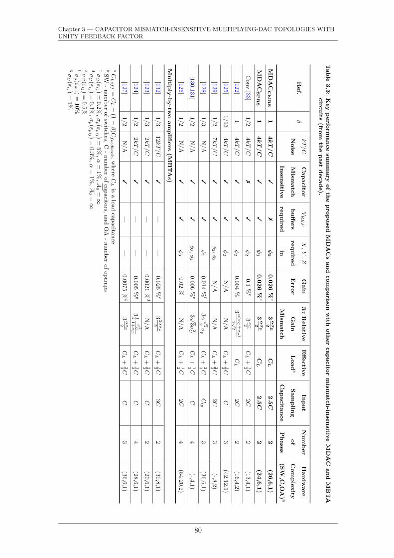
Chapter 3 — CAPACITOR MISMATCH-INSENSITIVE MULTIPLYING-DAC TOPOLOGIES WITHUNITY FEEDBACK FACTOR
Table
3.3
:K
ey
perfo
rmance
sum
mary
of
the
pro
pose
dM
DA
Cs
and
com
pariso
nw
ithoth
er
capacito
rm
ismatch
-inse
nsitiv
eM
DA
Cand
MB
TA
circ
uits
(from
the
past
decade).
Ref.
βkT/C
Capacito
rVREF
X,Y
,Z
Gain
3σ
Rela
tive
Eff
ectiv
eIn
put
Num
ber
Hard
ware
Noise
Mism
atch
buff
ers
require
dE
rror
Gain
Load
aSam
plin
gof
Com
ple
xity
Inse
nsitiv
ere
quire
din
Mism
atch
Capacita
nce
Phase
s(S
W,C
,OA
)b
MD
AC
CM
RS
14kT/C
37
φ2
0.0
26
%c
3ασp
2CL
2.5C
2(2
6,6
,1)
MD
AC
SPR
S1
4kT/C
33
φ1
0.0
26
%c
3ασp
2CL
2.5C
2(2
4,6
,1)
Conv.[3
3]
1/2
4kT/C
73
φ2
0.1
%c
3σC2
CL
+12C
2C
2(1
3,4
,1)
[122]
14kT/C
33
φ2
0.0
04
%3α
(σC
+σp)
2 √2
CL
2C
2(1
6,4
,2)
[125]
1/13
4kT/C
33
φ2
N/A
N/A
CL
+12C
C3
(42,1
2,1
)
[129]
1/2
7kT/C
33
φ2 ,φ
3N
/A
N/A
CL
+23C
2C
3(-,8
,2)
[128]
1/3
N/A
33
φ1
0.0
14
%f
3α√
22σp
CL
+23C
Cip
3(3
6,6
,1)
[130,1
31]
1/2
N/A
33
φ3 ,φ
40.0
06
%e
3 √3σ
2CCL
+12C
C4
(-,4,1
)
[126]
1/2
N/A
33
φ3
0.0
2%
N/A
CL
+12C
2C
4(5
4,2
0,2
)
Multip
ly-b
y-tw
oam
plifi
ers
(MB
TA
s)
[132]
1/3
12kT/C
3—
—0.0
25
%c
32ασp
5CL
+13C
3C
2(3
0,8
,1)
[123]
1/3
2kT/C
3—
—0.0
021
%d
N/A
CL
+23C
C2
(20,6
,1)
[124]
1/2
2kT/C
3—
—0.0
05
%g
314
σ2C
1+σC
CL
+12C
C4
(28,6
,1)
[127]
1/2
N/A
3—
—0.0
075
%g
3ασp
2CL
+23C
C3
(36,6
,1)
aCLeff
=CL
+(1−β
)Cfeedback,
where
CL
isa
load
capacita
nce
bSW
-num
ber
of
switch
es,C
-num
ber
of
capacito
rs,and
OA
-num
ber
of
opam
ps
cσC
(εij )
=0.2
%,σp (ε
pij )
=5%
,α
=1%
,A
0=∞
dσC
(εij )
=0.3
%,σp (ε
pij )
=0.3
%,α
=1%
,A
0=∞
eσC
(εij )
=0.5
%fσp (ε
pij )
=10%
gσC
(εij )
=1%
80

Chapter 4
Application of CircuitEnhancement Techniques to ADCBuilding Blocks
4.1 Overview
In the first section of this chapter, a 1.5-bit flash quantizer is proposed. This fully differen-
tial flash quantizer has built-in thresholds, made possible by employing inverter structures
as input devices. Self-biasing techniques are employed for enhanced PVT robustness.
Various analyses (confirmed with simulations) are carried out to describe the circuit’s
functionality, such as, kickback noise, regeneration time, metastability, offset, sensitivity
to common-mode variations, and finally, a working proof of a pipeline ADC that employs
the proposed circuit in all stages is given. A design procedure is also described and the
section is concluded with a performance summary and a comparative table.
The second section of this chapter presents a two-stage amplifier with enhanced perfor-
mance. Energy efficiency is improved by using inverter-input structures, which effectively
double the transconductance of the circuit for the same current. Self-biasing is employed
in both stages for improved PVT robustness and further power reduction. The analyses
carried out include differential-mode and common-mode feedback, noise, offset, slew rate,
input-output ranges, and some considerations are given what concerns the amplifier’s class
of operation. Finally, guidelines are given for a successful design and a genetic algorithm
optimization procedure is briefly described.
81

Chapter 4 — APPLICATION OF CIRCUIT ENHANCEMENT TECHNIQUES TO ADC BUILDINGBLOCKS
4.2 Inverter-Based Self-Biased 1.5-bit Flash Quantizer
Conventional 1.5-bit quantizers employ 2 comparators followed by a binary XYZ encoder.
Normally each comparator has an input switched-capacitor (SC) network, which defines
the threshold voltage (VTH = ±VREF /4), followed by a dynamic pre-amplifier stage (pre-
amp), a dynamic positive feedback latch (PFBL), and an SR digital latch. In advanced
CMOS technologies with low supply voltages, the use of the pre-amp attenuates metasta-
bility problems (caused by the reduced signal swing). Large devices are used in the pre-amp
and PFBL to reach the required accuracy (offset), leading to a poor energy efficiency. In
[133], for example, the pre-amp stage is embedded into the SC network by employing MOS
parametric amplification, but an input SC network is still required. The input SC network
can be avoided if built-in threshold levels are created by threshold inverter quantization
[134] or by using quantum voltage comparators [135]. Although the techniques in [134]
and [135] can be readily applied in low-medium resolution flash quantizers [136,137], they
are unsuitable for pipeline ADCs, since only a single-ended input can be accepted. More-
over, the circuits based on these techniques are highly sensitive to process, supply, and
temperature (PVT) variations and mismatch.
In the proposed flash quantizer, the improvement of energy efficiency is achieved by
proposing a fully differential 1.5-bit quantizer that relies on a simple circuit based on in-
verters with built-in threshold voltages. Self-biasing together with the proposed design
procedure makes the circuit highly robust to PVT variations and mismatch. The gener-
alization for sub-ADCs with higher resolutions (up to 3.5 or 4 bits) is straightforward,
since any pair of symmetrical threshold voltages is easily built. Although the main appli-
cation of this circuit targets pipeline ADCs, it is directly applicable in other types of A/D
architectures, namely, multi-stage algorithmic and multi-step flash.
Simulation results, in standard 65 nm and 0.13 µm CMOS technologies, demonstrate
that following the suggested design methodology, the proposed flash quantizer is capable
of achieving low offset, low kickback noise, low metastability probability errors and fast
regeneration time with very low power dissipation, leading to an enhancement in energy
efficiency.
82

4.2 — INVERTER-BASED SELF-BIASED 1.5-BIT FLASH QUANTIZER
1
1
1'
Vip
Vin
VCMI
Sampling
circuit
(optional)
VCM
Vinp
Vinn
VSS
VDD
M5
MP1
MN1
10/0.17
40/0.12 40/0.12
MP2
MN2
20/0.17
4/0.15
MP3
MN3
INV1 INV2 INV3
VB
VA
VC
Vop Von
M4A
INV5 INV6
M4B
IB
(10/0.24)
(13.5/0.24)
(20/0.24)
(4/0.24)(13.5/0.24)
10/0.17
(10/0.24)
Vinp Vinn VCM
5.3/0.84
(3.9/1)
7.5/0.28
(4/1)
32/0.17
(32/0.24)
(a)
D Q
Q
D
Q
Q
clkVonL
VopL
VonL
Vop
Von
VopL
clk clk
clk
clk
clk
clk
clk
clk
DQ
QXYZ
Encoder
VonLVopL X
Y
ZVopLVonL
(b) (c)
Figure 4.1: Proposed 1.5-bit flash quantizer: (a) Complete circuit with optional samplingcircuit and VCM generator. (b) D flip-flops. (c) XYZ encoder. All transistorsizes (W/L) are in µm. Sizes without brackets are for a 65 nm technology andthose within brackets are for a 0.13 µm one.
4.2.1 Principle of Operation
The 1.5-bit flash quantizer, illustrated in Fig. 4.1a, has three main inverters. INV1 and
INV2 are connected to the differential input signal while INV3, the self-biasing inverter,
has at its input a common mode voltage (VCM ). The differential circuit composed of
INV1 and INV3, defines one threshold voltage. Likewise, INV2 and INV3 form another
differential circuit, which define the symmetric threshold voltage. Assuming that the
input common-mode voltage is approximately VCM , it is possible to extract the following
relationships VGSN1 − VGSN3 + VDS4A − VDS4B = +Vid/2
VSGP1 − VSGP3 = −Vid/2(4.1a)
VGSN2 − VGSN3 + VDS4A − VDS4B = −Vid/2
VSGP2 − VSGP3 = +Vid/2
(4.1b)
83

Chapter 4 — APPLICATION OF CIRCUIT ENHANCEMENT TECHNIQUES TO ADC BUILDINGBLOCKS
where Vid = Vinp − Vinn represents the differential input voltage. The two threshold1
(switching) voltages of the quantizer (±VTH) are the corresponding values of Vid when Vop
or Von reaches (VA − VB)/2, or when the differential output signal Vod (= Vop − Von) is
approximately VDD/2, as shown in Fig. 4.2a.
The proposed 1.5-bit flash quantizer comprises another two inverters (INV5 and INV6),
a current source (M5) and two transistors operating in the triode region (M4A and M4B).
The two extra inverters together with the D-type Flip-Flops (D-FFs) regenerate the output
signals from INV1 and INV2, which strongly reduces the comparison (regeneration) time.
Fig. 4.2b displays the simulated outputs of INV1 and INV2 as well as the outputs of INV5
and INV6 (Vop and Von). The latter are connected to CMOS switched-inverter D-FFs (see
Fig. 4.1b), followed by an XYZ encoder (Fig. 4.1c). The differential output signal, Vod (or
VodL, where L stands for latched), has three possible logic states -1, 0, and 1, as shown
in Fig. 4.2a, which are used to build the outputs of the 1.5-bit flash quantizer. These
possible logic states permit representing the outputs of the XYZ encoder, respectively
given by X,Y , and Z.
PMOS current source, M5, has its gate voltage controlled by the output of the self-
biasing inverter (INV3), and is connected to the circuit in a negative feedback loop. This
loop reduces the effect of supply and process variations. As an example, if VDD increases,
VSGP5 also increases producing an increase in the bias current, IB. This will proportionally
change the current in the main inverters. Since MP3 is tied to a constant gate and source
voltage (VCM and VA), VSGP3 will remain constant but the rising current flowing through
MP3 will cause VC to increase. Therefore, VSGP5 = VDD − VC , will remain approximately
constant and compensate the VDD variation. Process variations have similar compensa-
tions through the negative feedback loop. Moreover, the feedback loop also stabilizes the
bias voltages when variations in device parameters or operating conditions occur. Tran-
sistors M4A and M4B are always biased in the triode region, which is guaranteed by their
high (and nearly constant) gate voltage, VA. Since these two devices can have different
dimensions, transistor M4B introduces a degree of freedom, which can be used to optimize
the temperature compensation, particularly in deep submicron CMOS technologies.
Comparing with the self-biasing amplifier/comparator in [138] the circuit proposed
here has significant differences and improvements:
1Not to be confused with the threshold voltage of a transistor.
84

4.2 — INVERTER-BASED SELF-BIASED 1.5-BIT FLASH QUANTIZER
−0.5 0 0.5
−1
−0.5
0
0.5
1
Vid, V
Vod,V
+VTH−VTH
Vod
Vid
(a)
−0.5 0 0.5
0
0.5
1
1.5
Vid, V
V,V
+VTH−VTH
Vop Von VoINV 1VoINV 2
(b)
Figure 4.2: Input-output waveforms: (a) Differential output (Vod = Vop−Von) and differentialinput signal, Vid. (b) Single-ended outputs of INV1, INV2, INV5 and INV6.
• two differential inverter comparator structures are merged by sharing the self-biasing
inverter;
• two built-in threshold levels are obtained by suitable sizing of transistors MN1−3,
MP1−3;
• M5 is biased in the saturation region rather than in the triode region, thus reducing
the effect of supply voltage variations;
• the gate voltage of M4A is VA instead of VC , which improves both stability and
temperature compensation;
• as in [134–137], two standard-sized inverters (INV5 and INV6) improve regeneration
time and reduce metastability;
• transistor M4B is added to further improve temperature compensation in deep-
submicron CMOS technologies.
85

Chapter 4 — APPLICATION OF CIRCUIT ENHANCEMENT TECHNIQUES TO ADC BUILDINGBLOCKS
4.2.2 Circuit and Performance Analysis
Circuit Analysis
Advanced CMOS technologies lead to the reduction of the supply voltage, which in turn
cause the transistors to operate in weak-to-moderate inversion regions. This situation
becomes exacerbated in circuits with many stacked transistors, which is the case of the
present circuit. Therefore, it is probable that all transistors of the three main inverters
operate in weak-to-moderate inversion. The low biasing currents and with VOD (overdrive
voltage, VOD = VGS−VTH) less than 100 mV [139] will lead to operation in these regions.
The ID-VGS characteristic of these transistors is (approximately) exponential, given by
ID = ID0W
LeVGSnVt (4.2)
where ID0 represents a characteristic current, W and L are the width and length of the
transistor, n is the subthreshold slope coefficient, and Vt = kT/q ≈ 26 mV (at room
temperature) is the thermal voltage. Coefficient n depends on the biasing and thus is
not accurately known. The values of n and ID0 can be extracted from simulation data.
To extract the values of these parameters, the exponential approximation of the ID-VGS
curve of MP2 depicted by the top plots of Fig. 4.3a and Fig. 4.3b is used. For the 0.13 µm
technology, n ≈ 1.9 and for the 65 nm technology, n ≈ 1.6. As suggested in [139] a
good procedure to verify a transistor in terms of its region of operation is to analyse its
log(ID)-VGS curve. This is depicted in the bottom plots of Fig. 4.3a and Fig. 4.3b for both
technologies. As can be seen, the section where the graph is approximately linear defines
the weak inversion region. Where the graph becomes more rounded defines the moderate
inversion region. For the 0.13 µm process there is quite a reasonable approximation to
the strong inversion equation near the switching VGS , which does not occur for the 65 nm
process, suggesting that, for this technology, the transistors operate in a weak-to-moderate
inversion region.
86

4.2 — INVERTER-BASED SELF-BIASED 1.5-BIT FLASH QUANTIZER
0.3 0.4 0.5 0.60
2
4
6x 10
−5
I D,A
ID(VGS)
1.02 × 10⁻¹⁰eVGS
1.6·0.026
0.3 0.4 0.5 0.6−10
−8
−6
−4
−2
VGS , V
log(I
D),
A
Switching VGS
Weak Moderate
Weak inversion eq.
Strong inversion eq.
(a)
0.2 0.3 0.4 0.50
0.5
1x 10
−4
I D,A
ID(VGS)
1.05 × 10⁻⁸eVGS
1.9·0.026
0.2 0.3 0.4 0.5−10
−8
−6
−4
−2
VGS , V
log(I
D),
A
Switching VGS
Weak Moderate/Strong
Weak inversion eq.
Strong inversion eq.
(b)
Figure 4.3: ID − VGS and log(ID) − VGS curves of the PMOS transistors of INV1,2 for: (a)65 nm process and (b) 0.13 µm process.
87

Chapter 4 — APPLICATION OF CIRCUIT ENHANCEMENT TECHNIQUES TO ADC BUILDINGBLOCKS
0 20 40 60 80 1000
50
100
150
200
WN 1WP2
WP1WN 2
VTH,mV
0.13 µm
65 nm
Theoretical curve of VTH
Simulation data
Figure 4.4: Theoretical curve of the quantizer’s threshold voltage, VTH , and simulation datapoints, for the 65 nm and 0.13 µm technologies.
To determine the switching threshold voltage, VTH , a derivation from Eq. 4.1b and
Eq. 4.2 is used. By writing Eq. 4.2 for VGS(ID), and substituting it in Eq. 4.1b, we obtain
− nVt ln
(IDN2
ID0N2
LN2
WN2
)+ nVt ln
(IDN3
ID0N3
LN3
WN3
)− (VDS4A − VDS4B) =
VTH2
+ nVt ln
(IDP2
ID0P2
LP2
WP2
)− nVt ln
(IDP3
ID0P3
LP3
WP3
)− (VDS4A − VDS4B) =
VTH2.
(4.3)
By taking into account that IDN2 = IDP2 and IDN3 = IDP3, by assuming that ID0N2 =
ID0P2, ID0N3 = ID0P3 , LN2 = LP2, LN3 = LP3, by summing both expressions of Eq. 4.3
and by applying simple logarithmic math, the following expression for the switching thresh-
old voltage is obtained
VTH = FnVt ln
(WN2WP3
WP2WN3
)− (VDS4A − VDS4B), (4.4)
where F is a fitting parameter. Eq. 4.4 represents an expression that defines the switching
threshold voltage of the 1.5-bit flash quantizer as a function of the transistors’ widths
(transistor lengths are easily included). Regarding VDS4A,B, transistors M4A,B will operate
in the linear region and therefore are easily sized using known equations. An expression
similar to Eq. 4.3 and Eq. 4.4 can be derived combining Eq. 4.1a and Eq. 4.2 for defining
the negative threshold voltage, −VTH . This is unnecessary because as long as WN1 = WN2
and WP1 = WP2, the threshold voltage will be symmetric around 0 V, i.e., ±VTH will be
88
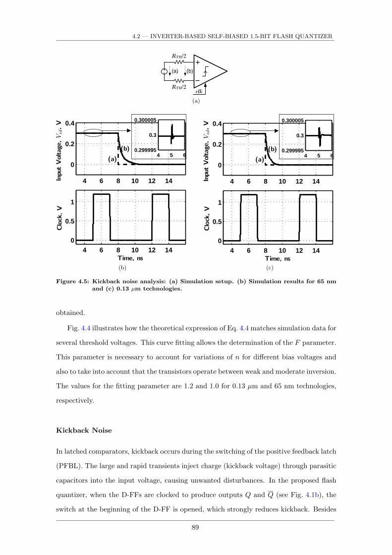
4.2 — INVERTER-BASED SELF-BIASED 1.5-BIT FLASH QUANTIZER
RTH/2
RTH/2
+
clk
(a) (b)
(a)
4 6 8 10 12 14
0
0.2
0.4
InputVoltage
,Vid,V
(a)
(b)
4 6 8 10 12 140
0.5
1
Clock,V
Time, ns
4 5 60.299995
0.3
0.300005
(b)
4 6 8 10 12 14
0
0.2
0.4
InputVoltage
,Vid,V
(a)
(b)
4 6 8 10 12 140
0.5
1Clock,V
Time, ns
4 5 60.299995
0.3
0.300005
(c)
Figure 4.5: Kickback noise analysis: (a) Simulation setup. (b) Simulation results for 65 nmand (c) 0.13 µm technologies.
obtained.
Fig. 4.4 illustrates how the theoretical expression of Eq. 4.4 matches simulation data for
several threshold voltages. This curve fitting allows the determination of the F parameter.
This parameter is necessary to account for variations of n for different bias voltages and
also to take into account that the transistors operate between weak and moderate inversion.
The values for the fitting parameter are 1.2 and 1.0 for 0.13 µm and 65 nm technologies,
respectively.
Kickback Noise
In latched comparators, kickback occurs during the switching of the positive feedback latch
(PFBL). The large and rapid transients inject charge (kickback voltage) through parasitic
capacitors into the input voltage, causing unwanted disturbances. In the proposed flash
quantizer, when the D-FFs are clocked to produce outputs Q and Q (see Fig. 4.1b), the
switch at the beginning of the D-FF is opened, which strongly reduces kickback. Besides
89

Chapter 4 — APPLICATION OF CIRCUIT ENHANCEMENT TECHNIQUES TO ADC BUILDINGBLOCKS
this, from the output Vod to the input Vid there are a cascade of parasitic capacitors, i.e.,
series of the equivalent Cgd of INV5,6 with the equivalent Cgd of INV1,2, which reduces
the parasitic capacitance from output to input. The kickback voltage is analysed using
an identical simulation setup to the one proposed in [39], illustrated in Fig. 4.5a (RTH =
8 kΩ), with the results shown in Fig. 4.5b and Fig. 4.5c. The kickback during switching
is approximately 4 µV and 3 µV, for the 65 nm and 0.13 µm technologies, respectively.
However, the proposed circuit’s outputs, Vod, may vary before any clocking occurs,
given its analog architecture. These outputs may change from rail-to-rail depending on
the actual input. This will inject charge into the input voltage through the series parasitic
capacitances mentioned above. Naturally the amount of charge injected is highly depen-
dent on the sizing of the transistors of the inverters. For the 65 nm technology (transistor
sizes are those shown in Fig. 4.1a) the injected charge results in an added voltage of 9.7 mV
and 18.5 mV for a rising and falling output, respectively. For the 0.13 µm technology the
added voltage due to charge injection is 6 mV and 12.6 mV for a rising and falling output,
respectively. The proposed sampling circuit (on the right of Fig. 4.1a) helps isolate the
input voltage from any disturbances caused by kickback.
Regeneration Time
In the proposed architecture the regeneration time (or recovery time) may be defined as
the time it takes the output, VodL, to reach a valid logic value (considering the D-FFs are
in a transparent state). It will be considered that 0.2 V represents a logic 0 and 1 V, a
logic 1. To determine the regeneration time, the method suggested in [38] is employed.
This method assesses the flash quantizer’s speed performance by testing it for two extreme
cases. The first case consists of a full-scale input, VFS , that changes to VTH + 1 LSB. For
the second case, the input goes from VFS to VTH − 1 LSB with the objective of causing
indecision, and therefore the output needs to recover. The time it takes the outputs to
reach logic values determines the maximum operating rate of the flash quantizer.
As can be seen by the voltage waveforms of Fig. 4.2, for each threshold voltage, one of
the outputs, Vop or Von, changes polarity. Depending on the input voltage, both outputs
might end up changing, e.g., when the input changes from +VFS to below −VTH or from
−VFS to above +VTH . This is considered the worst-case, therefore, the regeneration time
is simulated for this situation. The resultant waveforms (Vid and VodL) for three accuracy
90

4.2 — INVERTER-BASED SELF-BIASED 1.5-BIT FLASH QUANTIZER
0 0.5 1 1.5 2 2.5 3 3.5 4
−1
−0.5
0
0.5
1
Time, ns
Vid
andVodL,V
+VTH
Vid
VodL
regen.time
2-bit3-bit4-bit
Figure 4.6: Regeneration time of the output, VodL, for various accuracies.
situations (2, 3, and 4-bit) are illustrated in Fig. 4.6, for the 65 nm case only. The input
goes from −VFS to +VTH ±1 LSB, with VFS = 0.5 V, VTH = 0.125 V, and VREF = 0.5 V.
For the first test, +VTH + 1 LSB, it can be seen that the output has an initial change
of polarity, due to the negative threshold voltage, and then another change in polarity,
much more prolonged due to the positive threshold. The second change is more prolonged
because the input voltage is very close to the threshold voltage (+1 LSB). The closer the
input is to the threshold voltage, the longer the regeneration time2. The output then
returns to 1.2 V because the input is at −VFS again and this starts the second test: the
input goes from −VFS to +VTH − 1 LSB. As can be seen, there is the initial change of
polarity (due to −VTH), but, although the input is close to the threshold voltage, the
output stays constant and no indecision is visible.
Table 4.1 summarizes the regeneration times for various accuracies and for both tech-
nologies. Note that the flash quantizer sized for each technology was not optimized for
speed. Therefore, the regeneration times for the 0.13 µm technology appeared faster. Note
also that, the current consumption for the 65 nm case is less than half that of 0.13 µm
case (see Table 4.3 for details).
2With an input exactly equal to the threshold voltage, the regeneration time would be infinitely long,leading to a situation of metastability.
91

Chapter 4 — APPLICATION OF CIRCUIT ENHANCEMENT TECHNIQUES TO ADC BUILDINGBLOCKS
Table 4.1: Regeneration times for various accuracies and both technologies (VREF = 0.5 V).
Accuracy (bits) LSB (mV) Regeneration Time (ps) Max. sampling rate (GS/s)
65 nm
2 125 484 2.0
3 62.5 615 1.6
4 31.25 814 1.2
6 7.8 1580 0.6
8 2 2569 0.4
0.13 µm
2 125 280 3.5
3 62.5 405 2.5
4 31.25 612 1.6
6 7.8 1108 0.9
8 2 1520 0.65
GBW = gm /CL
VSS
VDD
M5
MP3
MN3
INV1
INV3
Vo
M4A
INV5
M4B
Vi VCMgm
INVD-FF
CL CL CL CL
gm gm gm
A1 A2 A3 A4
Figure 4.7: Equivalent circuit for metastability analysis considering a multistage approach.Single-ended shown for simplicity.
Probability of Metastability
The proposed quantizer relies on a pipeline architecture as shown in Fig. 4.7, i.e., a cascade
of open-loop amplifiers (inverters), to produce the final outputs. Therefore, assuming that
the D-FFs are in writing mode there is, in fact, a cascade of four inverters before the
XYZ encoder. These inverters are composed of INV1 (or INV2) followed by INV5 (or
INV6), and two inverters from the D-FF (see Fig. 4.1). In order to calculate the final
time constant of this kind of architecture, the method for multistage amplifiers proposed
in [140] is used.
The time constant is defined by
τ = τm
(VoVi×N !
)1/N
=1
GBW
(VoVi×N !
)1/N
, GBW = gm/CL, (4.5)
92
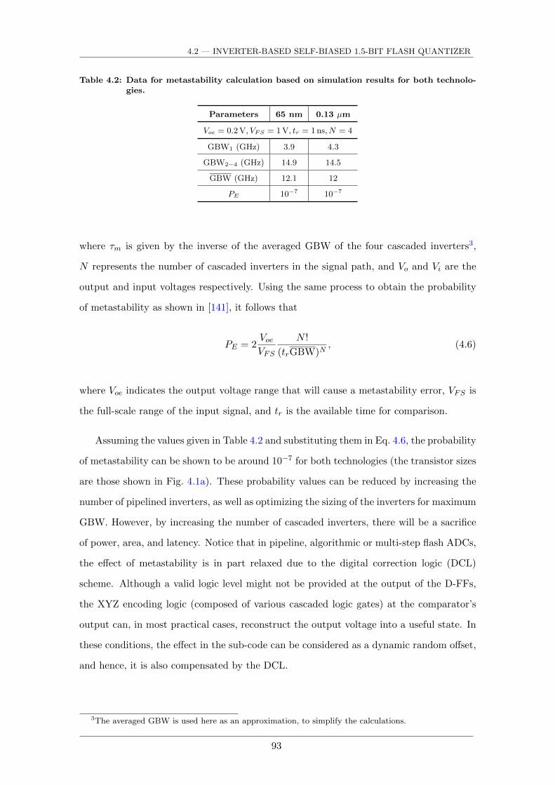
4.2 — INVERTER-BASED SELF-BIASED 1.5-BIT FLASH QUANTIZER
Table 4.2: Data for metastability calculation based on simulation results for both technolo-gies.
Parameters 65 nm 0.13 µm
Voe = 0.2 V, VFS = 1 V, tr = 1 ns, N = 4
GBW1 (GHz) 3.9 4.3
GBW2−4 (GHz) 14.9 14.5
GBW (GHz) 12.1 12
PE 10−7 10−7
where τm is given by the inverse of the averaged GBW of the four cascaded inverters3,
N represents the number of cascaded inverters in the signal path, and Vo and Vi are the
output and input voltages respectively. Using the same process to obtain the probability
of metastability as shown in [141], it follows that
PE = 2VoeVFS
N !
(trGBW)N, (4.6)
where Voe indicates the output voltage range that will cause a metastability error, VFS is
the full-scale range of the input signal, and tr is the available time for comparison.
Assuming the values given in Table 4.2 and substituting them in Eq. 4.6, the probability
of metastability can be shown to be around 10−7 for both technologies (the transistor sizes
are those shown in Fig. 4.1a). These probability values can be reduced by increasing the
number of pipelined inverters, as well as optimizing the sizing of the inverters for maximum
GBW. However, by increasing the number of cascaded inverters, there will be a sacrifice
of power, area, and latency. Notice that in pipeline, algorithmic or multi-step flash ADCs,
the effect of metastability is in part relaxed due to the digital correction logic (DCL)
scheme. Although a valid logic level might not be provided at the output of the D-FFs,
the XYZ encoding logic (composed of various cascaded logic gates) at the comparator’s
output can, in most practical cases, reconstruct the output voltage into a useful state. In
these conditions, the effect in the sub-code can be considered as a dynamic random offset,
and hence, it is also compensated by the DCL.
3The averaged GBW is used here as an approximation, to simplify the calculations.
93

Chapter 4 — APPLICATION OF CIRCUIT ENHANCEMENT TECHNIQUES TO ADC BUILDINGBLOCKS
Offset
One the main limitations of comparator circuits is offset, i.e., deviations to the nominal
switching threshold. These deviations can limit the performance of ADCs, namely by
reducing or increasing the ADC’s full-scale range. Offsets may occur due to mismatch
between symmetric devices or in components that alter the operating point of the circuit.
In the proposed flash quantizer, symmetric transistors are MP1 and MP2, and MN1 and
MN2. Any mismatch between these devices will offset the threshold voltage. Regarding
devices that may alter the circuit’s operating point, these are all the others. Of these
devices the ones that do not have a large influence on the threshold voltage are M5, M4A,
and M4B, while transistors MP3 and MN3 have a significant effect.
Mismatch may exist in various transistor parameters, namely, VTH , W , L, Cox, and µ.
Mathematically, these mismatches are given by [142,143]
∆VTH =AVTH,k√WL
k = N,P, (4.7a)
∆β =Aβ,k√WL
k = N,P, (4.7b)
where β = µCoxW/L, and AVTH and Aβ are area proportionality constants defined by the
process technology. It has been demonstrated in [44,45], that the total offset referred to a
transistor’s gate is given by
Vos,gate =(VGS − VTH)
2
(∆(W/L)
W/L
)+ ∆VTH . (4.8)
To determine the total input-referred offset voltage, Vos,in, a set of transfer functions (Hi)
need to be determined, such as the H from each offset voltage source (Vos,i) to the output,
and the open-loop DC gain (A = Vod/Vid) of the flash quantizer. Each offset voltage
is referred to the input by multiplying the respective Vos,i by the square of its transfer
function and then dividing the result by the DC gain squared. It is important to remember
to take the square (variance) of Eq. 4.8. The final input-referred offset voltage is then the
root of the sum of each input-referred Vos. Considering only the ∆VTH mismatch of Eq. 4.8,
which is the largest contributor (this simplification still yields a good approximation), the
94
4.2 — INVERTER-BASED SELF-BIASED 1.5-BIT FLASH QUANTIZER
input-referred offset is given by,
Vos,in =
√√√√ n∑i=1
(A2VTH,i
(WL)i
H2i
A2DC
). (4.9)
where n represents each transistor.
The transfer functions and open-loop DC gain are too complex to maintain a sufficient
level of accuracy to gain insight to the circuit and, therefore, are not shown here. Nev-
ertheless, a method has been given to determine the offset voltage and simulation results
will be shown instead. Monte Carlo simulation results (500 cases) for both technologies
are shown in Fig. 4.8, for the negative (top row) and positive (bottom row) threshold
voltages. The graphs on the left of Fig. 4.8 correspond to the worst-case threshold voltage
that occurs below the nominal VTH (±125 mV), while the graphs on the right are for the
worst-case threshold above the nominal VTH . For these simulations the transistor sizes of
Fig. 4.1a are used. Besides mismatch variations, process, supply voltage and temperature
(PVT) are also varied. The variations considered are typical-typical (tt), slow-slow (ss),
and fast-fast (ff) for process, 1.2 V ± 5 % for the supply voltage, and -40 C, 27 C, and
85 C for temperature. For the 65 nm technology, with nominal temperature (27 C) and
supply voltage (1.2 V), ±VTH has an average value of 125 mV and a standard deviation
of 8.1 mV. The minimum threshold voltage VTHmin = ±116.2 mV (in average) is obtained
for -40 C and 1.26 V supply. The maximum value, VTHmax = ±128.9 mV, is obtained
for 27 C and 1.14 V supply. The worst-case standard deviation obtained is 8.5 mV.
Regarding the 0.13 µm technology, in nominal conditions VTH has an average value of
approximately 125 mV and a standard deviation of 7 mV. The minimum threshold volt-
age VTHmin = ±109 mV is obtained for 85 C and 1.26 V supply. The maximum value,
VTHmax = ±129 mV, is obtained for 27 C and 1.14 V supply. The worst-case standard
deviation obtained is 7.7 mV.
Fig. 4.9 depicts the threshold voltage (average value) deviation with respect to PVT
variations. The objective of this graph is to illustrate the tendency of the threshold voltage
as a function of the aforementioned PVT variations. For the 65 nm technology, VTH varies
approximately 6 % for the full supply voltage range (considering all process and tempera-
ture variations). For a given supply voltage, VTH varies with temperature approximately
6.5 % and for the three process corners considered, less than 2.5 %. Regarding the 0.13 µm
95

Chapter 4 — APPLICATION OF CIRCUIT ENHANCEMENT TECHNIQUES TO ADC BUILDINGBLOCKS
−150 −125 −1000
30
601.26 V, -40 C
Sam
ples
µ=-115.8mVσ=8.5mV
−150 −125 −1000
30
601.2 V, 27 C
µ=-125.1mVσ=8.1mV
−150 −125 −1000
30
601.14 V, 27 C
µ=-128.9mVσ=8.0mV
100 125 1500
30
601.26 V, -40 C
Sam
ples
µ=116.5mVσ=8.0mV
100 125 1500
30
601.2 V, 27 C
VTH , mV
µ=124.9mVσ=7.7mV
100 125 1500
30
601.14 V, 27 C
µ=128.8mVσ=7.6mV
(a)
−150 −125 −1000
30
601.26 V, 85 C
Sam
ples
µ=-108.8mVσ=7.7mV
−150 −125 −1000
30
601.2 V, 27 C
µ=-124.8mVσ=7.0mV
−150 −125 −1000
30
601.14 V, 27 C
µ=-128.8mVσ=6.8mV
100 125 1500
30
601.26 V, 85 C
Sam
ples
µ=109.2mVσ=7.4mV
100 125 1500
30
601.2 V, 27 C
VTH , mV
µ=125.1mVσ=6.8mV
100 125 1500
30
601.14 V, 27 C
µ=129.2mVσ=6.6mV
(b)
Figure 4.8: Histograms for 500 Monte Carlo simulations considering PVT corners and mis-match for the: (a) 65 nm process and (b) 0.13 µm technology. Top and bottomrow show the negative and positive threshold voltage, respectively. The meanvalue and standard deviation of the data are represented by µ and σ, respectively.
technology, VTH varies approximately 13 % for the full supply voltage range and for all
process and temperature variations. For a specific voltage, VTH varies with temperature
approximately 8.5 % and with process corners less than 12 %. Fig. 4.9 and the described
results indicate that the 65 nm technology shows much improved results, specially con-
cerning process and supply voltage variations. Furthermore, by analysing the graphs of
Fig. 4.9, which have an identical y-axis limits for comparison, it can be seen that the range
96
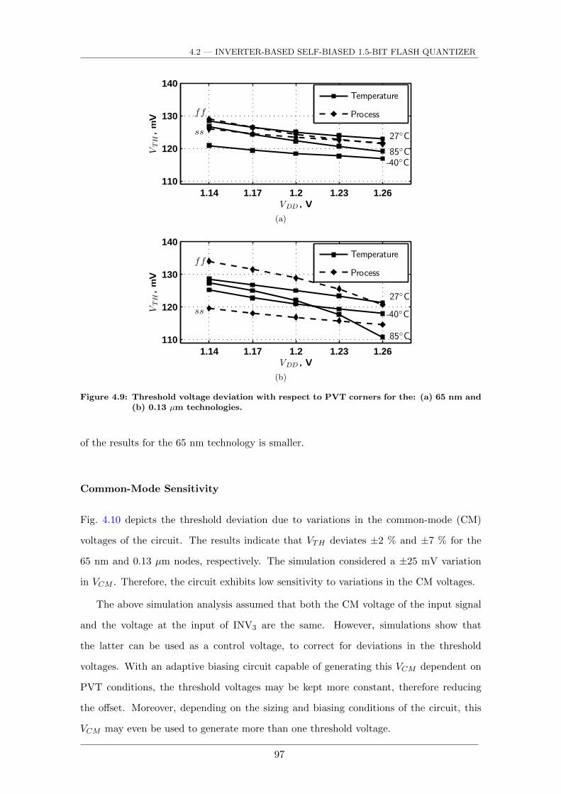
4.2 — INVERTER-BASED SELF-BIASED 1.5-BIT FLASH QUANTIZER
1.14 1.17 1.2 1.23 1.26110
120
130
140
VDD , V
VTH,mV
ss
ff
85C-40C
27C
Temperature
Process
(a)
1.14 1.17 1.2 1.23 1.26110
120
130
140
VDD , V
VTH,mV
ss
ff
85C
-40C
27C
Temperature
Process
(b)
Figure 4.9: Threshold voltage deviation with respect to PVT corners for the: (a) 65 nm and(b) 0.13 µm technologies.
of the results for the 65 nm technology is smaller.
Common-Mode Sensitivity
Fig. 4.10 depicts the threshold deviation due to variations in the common-mode (CM)
voltages of the circuit. The results indicate that VTH deviates ±2 % and ±7 % for the
65 nm and 0.13 µm nodes, respectively. The simulation considered a ±25 mV variation
in VCM . Therefore, the circuit exhibits low sensitivity to variations in the CM voltages.
The above simulation analysis assumed that both the CM voltage of the input signal
and the voltage at the input of INV3 are the same. However, simulations show that
the latter can be used as a control voltage, to correct for deviations in the threshold
voltages. With an adaptive biasing circuit capable of generating this VCM dependent on
PVT conditions, the threshold voltages may be kept more constant, therefore reducing
the offset. Moreover, depending on the sizing and biasing conditions of the circuit, this
VCM may even be used to generate more than one threshold voltage.
97

Chapter 4 — APPLICATION OF CIRCUIT ENHANCEMENT TECHNIQUES TO ADC BUILDINGBLOCKS
530 540 550 560 570115
120
125
130
135
VCM , mV
VTH,mV
130 nm65 nm
Figure 4.10: Threshold voltage deviation with respect to VCM variations for both technolo-gies.
Proof-of-Functionality
As a proof-of-functionality, the proposed flash quantizer circuit is employed in all sub-
ADCs of a real 7-bit 500 MS/s pipeline converter, designed in the 0.13 µm technology. The
converter is composed of five 1.5-bit stages and a final 2-bit stage. All 1.5-bit sub-ADCs
rely on the circuit shown in Fig. 4.1. For the final 2-bit stage, the quantizer’s thresholds
are ±250 mV and 0 V. For the ±250 mV thresholds the proposed circuit architecture
is used, but with a resizing of the transistors’ dimensions. The 0 V threshold is easily
achieved by eliminating INV1 (or INV2) and by making INV3 equal, i.e., the dimensions
of the transistors, to the inverter that remained (INV1 or INV2).
Fig. 4.11 shows the electrically simulated 8192-point FFT, DNL and INL results of the
pipeline ADC for a 200 MHz input signal. A SFDR of 45.5 dB and an SNDR of 41.4 dB
is obtained which leads to an ENOB of 6.6 dB. Concerning DNL and INL, the maximum
absolute values obtained are -0.32 and -0.59 LSBs respectively. These results demonstrate
the practical usefulness of the proposed 1.5-bit flash quantizer circuit since good DNL,
INL, and SNDR performance are achieved.
4.2.3 Design Procedure
To achieve a specific VTH , the following steps may be considered as a design procedure
and guidelines to an approximately accurate threshold voltage, when taking into account
98
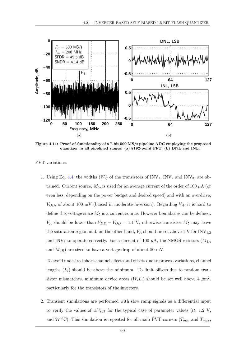
4.2 — INVERTER-BASED SELF-BIASED 1.5-BIT FLASH QUANTIZER
0 50 100 150 200 250−120
−100
−80
−60
−40
−20
0
Frequency, MHz
Amplitud
e,dB H3
FS = 500 MS/sfin = 206 MHzSFDR = 45.5 dBSNDR = 41.4 dB
(a)
0 64 127
−0.5
0
0.5
DNL, LSB
0 64 127
−0.5
0
0.5
INL, LSB
(b)
Figure 4.11: Proof-of-functionality of a 7-bit 500 MS/s pipeline ADC employing the proposedquantizer in all pipelined stages: (a) 8192-point FFT. (b) DNL and INL.
PVT variations.
1. Using Eq. 4.4, the widths (Wi) of the transistors of INV1, INV2 and INV3, are ob-
tained. Current source, M5, is sized for an average current of the order of 100 µA (or
even less, depending on the power budget and desired speed) and with an overdrive,
VOD, of about 100 mV (biased in moderate inversion). Regarding VA, it is hard to
define this voltage since M5 is a current source. However boundaries can be defined:
VA should be lower than VDD − VOD = 1.1 V, otherwise transistor M5 may leave
the saturation region and, on the other hand, VA should be set above 1 V for INV1,2
and INV3 to operate correctly. For a current of 100 µA, the NMOS resistors (M4A
and M4B) are sized to have a voltage drop of about 50 mV.
To avoid undesired short-channel effects and offsets due to process variations, channel
lengths (Li) should be above the minimum. To limit offsets due to random tran-
sistor mismatches, minimum device areas (WiLi) should be set well above 4 µm2,
particularly for the transistors of the inverters.
2. Transient simulations are performed with slow ramp signals as a differential input
to verify the values of ±VTH for the typical case of parameter values (tt, 1.2 V,
and 27 C). This simulation is repeated for all main PVT corners (Tmin and Tmax,
99

Chapter 4 — APPLICATION OF CIRCUIT ENHANCEMENT TECHNIQUES TO ADC BUILDINGBLOCKS
VDDmin and VDDmax , and process corners ss and ff).
3. Compensation over the entire temperature range is optimized, by adjusting M4A and
M4B with different dimensions. Since this will affect VTH , the width of MN1 and
MN2 should be fine tuned to restore the value of VTH .
4. Repeat steps 2 and 3 until the best performance is reached considering relevant
PVT corners. The common-mode (CM) voltage (VCM ≈ VDDmin/2) used as input
for INV3, must guarantee that all transistors in the three main inverters operate in
saturation. VCM can be directly provided by a bandgap circuit (always available in
any type of ADC) and no buffering is required since it is connected to gate terminals.
In a pipeline-like ADC, this VCM voltage is also normally used to adjust the output
CM voltage of the pipelined stages through dedicated CMFB circuits. Therefore,
this voltage will be readily available. Optionally, VCM can be generated using the
SC circuit shown on the right of Fig. 4.1a, which always guarantees that the input
CM voltage of the proposed quantizer is approximately VCM .
4.2.4 Performance Summary and Comparison
Table 4.3 summarizes the simulation results obtained from the analyses carried out in
this section. Besides this, a comparison is made with other comparator circuits found
the literature. The search is limited to the past ten years and with clocking frequencies,
FS ≥ 0.5 GS/s.
Regarding Table 4.3, the power column indicates twice the power consumed by the
respective comparator. This is done for a fair comparison, since the proposed work is a
1.5-bit flash quantizer, i.e., it has two comparators merged into one circuit. The resolution
column indicates the accuracy of the voltage step used to obtain either the metastability
or the regeneration (comparison) time. Some authors indicate the minimum voltage to
obtain a given metastability, while others indicate the step voltage (or differential input)
used for the regeneration time analysis. The maximum accuracy (N) possible, for each
of the presented circuits, is related with the PVTM-3σ offset (Off3σ), given by N <
log2(VFS/Off3σ), where VFS is the differential full-scale voltage of the input signal.
The results of Table 4.3 indicate that the proposed quantizer has a relatively slow
regeneration time, due to the fact that most of the other comparators employ a positive
100

4.2 — INVERTER-BASED SELF-BIASED 1.5-BIT FLASH QUANTIZER
feedback latch, which accelerates their decision time. The proposed quantizer achieves an
average metastability probability error, a better than average PVTM-3σ offset and one
of the leading energy efficiencies among the state-of-the-art. Notice however, that the
results of all (except [133]) comparators are from measured data, whereas the results of
the proposed circuit are extracted from electrical simulations. Regarding the applications
envisaged by each comparator, most may be applied in A/D converters, while others are
designed for receiver front-ends [144], hence its high clocking frequency.
101

Chapter 4 — APPLICATION OF CIRCUIT ENHANCEMENT TECHNIQUES TO ADC BUILDINGBLOCKS
Table
4.3
:Sim
ula
ted
perfo
rmance
sum
mary
and
com
pariso
nw
ithoth
er
com
para
tor
circ
uits
found
inth
elite
ratu
rein
the
past
decade
for
clo
ckin
gfre
quencie
s,FS≥
0.5
GS/s.
Tech
.Supply
Pow
era
FS
Reso
lutio
nR
egenera
tion
Meta
stability
Off
set
EE
c
(µm
)V
olta
ge
(V)
(µW
)(G
S/s)
(bits)
Tim
e(p
s)B
ER
bP
VT
M-3σ
(mV
)(fF
/conv.-ste
p)
This
work
0.0
65
1.2
133
22
484
10−9
27
33
This
work
0.1
31.2
231
22
280
10−10
33
58
[145]
0.0
91
80
110
122
-5.1
d40
[146]
0.0
91.2
78
0.5
--
-11.4
d78
[147]
0.0
91.2
450
2∼
2∼
60
-24
113
[148]
0.1
21.5
720
26
-10−
930
180
[149]
0.0
65
1.2
2600
7∼
564
-33
186
[150]
0.1
21.5
1168
3∼
7-
10−
948.3
195
[151]
0.1
21.5
1624
42
-10−
9150
203
[152]
0.1
81.8
700
1.4
--
-13.1
250
[133]
0.1
31.2
284
0.5
2165
-60.9
284
[153]
0.1
21.5
5300
6∼
2-
10−
669
442
[154]
0.1
81.8
3700
3.8
410
250
10−
13
44.4
482
[144]
0.1
11.2
10080
10
--
10−
12
-504
[155]
0.0
65
1.2
5760
56
104
10−
96
576
[156]
0.3
53.3
4000
16
--
150
2000
[157]
0.3
53.3
6600
1.2
6-
-0.6
d2750
aF
or
the
presen
tedreferen
ces,th
isco
lum
nin
dica
testw
iceth
ep
ower
consu
med
by
the
respectiv
eco
mpara
tor
bB
itE
rror
Rate
cE
nerg
yE
fficien
cy,EE
=P
ower/
2E
NO
BFS
,w
here
EN
OB
=1-b
itd
Req
uires
calib
ratio
n
102

4.3 — TWO-STAGE INVERTER-BASED SELF-BIASED OPAMP
4.3 Two-Stage Inverter-Based Self-Biased Opamp
The power reduction necessity and low supply voltage tendency of modern CMOS tech-
nologies has driven the evermore challenging design of amplifiers to have multiple gain
stages and possibly an output driver stage. In single stage amplifiers, high DC gain is
achieved using cascode devices, but this leads to reduced output swing (OS) due to the
low supply voltage. Maintaining a high DC gain requirement but now demanding high
OS would naturally lead to the use of a two-stage amplifier (probably fully differential
to double the OS). In two-stage amplifiers, where compensation is inevitable, the gain-
bandwidth product, GBW (usually a specification: achieve highest possible GBW), is
given by GBW(I) ≈ gm1(I)/CC , where gm1 represents the transconductance of the input
differential pair, CC , the compensation capacitance, and I, the biasing current of the input
stage. Admitting that the opamp is biased with constant current, I, and with CC being
mainly imposed by thermal noise constraints, then, one way of achieving higher GBW re-
lies on using an inverter structure in the input stage. This type of input stage, if properly
sized, effectively doubles the transconductance. Now gm1 = gmP + gmN , where gmP and
gmN respectively represent the transconductance of the PMOS and NMOS transistors that
constitute the inverter structure [45]. In the literature it is possible to find numerous other
techniques for increasing and compensating the GBW of single- and multi-stage amplifiers
[158–161], among others, mostly relying on multipath and feedforward techniques.
Single-stage inverter input amplifiers have already been presented in the past [138,162,
163]. The inverter amplifier of [138] adds an interesting feature which is self-biasing. The
advantages of amplifier self-biasing techniques are well known [138,164]:
• they simplify the implementation of amplifiers by removing biasing circuitry, thus
saving power and die area;
• any mismatches and variations in circuit performance due to deviations in biasing
voltages are highly attenuated;
• they enable circuits to be more insensitive to PVT variations.
In amplifiers, self-biasing techniques have mainly been applied to complementary folded-
cascode and single stage inverter-based topologies [138,164,165].
103

Chapter 4 — APPLICATION OF CIRCUIT ENHANCEMENT TECHNIQUES TO ADC BUILDINGBLOCKS
M21
M22a
M23a
Vb2
Va2
M24
IB1
VDD
M11
VSS
Vip
M12a
VinVop Von
IB2 VCM2
CCa CCb
M14a
Va1
Vba Vbb
VCM1N
Von1 Vop1CMFB2 CMFB1
VCM1P
VCMOVCMO
CCM
M12b
M13b
M14b
M22b
M23bM13a
Figure 4.12: Proposed two-stage inverter-based self-biased amplifier.
The work developed in this thesis proposes combining self-biasing and inverter-input
structures in a two-stage amplifier enhancing its efficiency and achieving higher PVT
robustness.
4.3.1 Principle of Operation
The proposed two-stage inverter-based self-biased amplifier is depicted in Fig. 4.12. It
consists of two cascaded inverter stages with approximately the same topology. The input
stage consists of an inverter input pair (M12a,b and M13a,b) connected to current sources,
M11 and M14. The latter devices bias and control the common-mode (CM) level of the
input stage. The output stage has a similar topology (except that nodes Vba and Vbb are
connected together to form node Vb2) and its input pair consists of transistors M22a,b and
M23a,b. The biasing of the output stage and its output CM level are controlled by M21 and
M24. Given M21 and M24’s biasing voltage, VCM2, these devices will probably operate in
the triode/saturation boundary region [138].
Regarding compensation, node Vba and Vbb have been separated, for the connection
104

4.3 — TWO-STAGE INVERTER-BASED SELF-BIASED OPAMP
C2a
C2b
C1a
C1b
Vop
Von
VCM2 VCMO
2
2
2
1
1
1
Va2
M31
Vb2
VCM2 VCMOVCM1P VCM1N
M33
M34M32
(a) (b)
Figure 4.13: Common-mode feedback circuits: (a) SC network for the output stage (CMFB2)and (b) continuous time CMFB circuit for the input stage (CMFB1).
of the compensation capacitors, CCa,b, thus avoiding the inefficient conventional Miller
compensation [166,167]. In a preliminary analysis, this compensation can be described
as a cascoded-Miller type, in the sense that CCa,b are connected to low impedance source
nodes. This method is adequate because there is no direct forward-path between the input
and output of the output stage, thus avoiding the presence of a possible positive low-
frequency zero in the transfer function (TF). Given that this method of compensation was
used (to avoid Miller compensation), there is source degeneration of M13a,b. Therefore,
these transistors will not have such a pronounced effect on the amplifier’s performance
parameters (e.g., GBW and DC gain) as M12a,b.
The common-mode feedback (CMFB) circuits shown in Fig. 4.13 define the CM control
voltages of both stages and simultaneously bias the whole amplifier. The amplifier’s output
CM level is adjusted through a dedicated switched-capacitor (SC) CMFB circuit, CMFB2,
as illustrated by Fig. 4.13a, where VCM2 = (Vop+Von)/2 [168]. VCM2 biases M21 and M24,
and is an input for CMFB1 (illustrated in Fig. 4.13b). CMFB1 is an inverter-based pair
which compares voltage VCM2 with a constant voltage, VCMO (normally provided by a
bandgap circuit), and generates voltages VCM1P and VCM1N which bias the input stage
and control its CM level. It should be noticed that CMFB1 is connected to nodes Va2
and Vb2, thus avoiding the use of extra biasing transistors. Transistors M31−34 can be
down-scaled versions of M22a,b and M23a,b, but for a better optimization of the amplifier
and biasing of transistors M11 and M14a,b, these should be sized separately. Capacitor
CCM (Fig. 4.12) is placed at node VCM1N for CM stabilization.
Self-biasing voltages VCM1P , VCM1N and VCM2 are connected to the main amplifier
through feedback loops thus reducing the effects of PVT variations and the effects caused
105
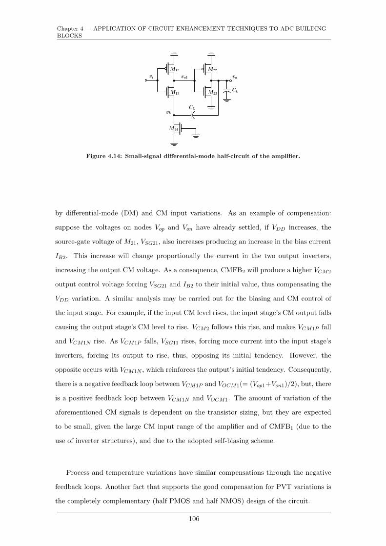
Chapter 4 — APPLICATION OF CIRCUIT ENHANCEMENT TECHNIQUES TO ADC BUILDINGBLOCKS
M22
M23
vi
M12
M13
vo
CC
M14
vb
vo1
CL
Figure 4.14: Small-signal differential-mode half-circuit of the amplifier.
by differential-mode (DM) and CM input variations. As an example of compensation:
suppose the voltages on nodes Vop and Von have already settled, if VDD increases, the
source-gate voltage of M21, VSG21, also increases producing an increase in the bias current
IB2. This increase will change proportionally the current in the two output inverters,
increasing the output CM voltage. As a consequence, CMFB2 will produce a higher VCM2
output control voltage forcing VSG21 and IB2 to their initial value, thus compensating the
VDD variation. A similar analysis may be carried out for the biasing and CM control of
the input stage. For example, if the input CM level rises, the input stage’s CM output falls
causing the output stage’s CM level to rise. VCM2 follows this rise, and makes VCM1P fall
and VCM1N rise. As VCM1P falls, VSG11 rises, forcing more current into the input stage’s
inverters, forcing its output to rise, thus, opposing its initial tendency. However, the
opposite occurs with VCM1N , which reinforces the output’s initial tendency. Consequently,
there is a negative feedback loop between VCM1P and VOCM1(= (Vop1+Von1)/2), but, there
is a positive feedback loop between VCM1N and VOCM1. The amount of variation of the
aforementioned CM signals is dependent on the transistor sizing, but they are expected
to be small, given the large CM input range of the amplifier and of CMFB1 (due to the
use of inverter structures), and due to the adopted self-biasing scheme.
Process and temperature variations have similar compensations through the negative
feedback loops. Another fact that supports the good compensation for PVT variations is
the completely complementary (half PMOS and half NMOS) design of the circuit.
106

4.3 — TWO-STAGE INVERTER-BASED SELF-BIASED OPAMP
4.3.2 Circuit Analysis
Differential-Mode Analysis
The small-signal DM equivalent circuit is shown in Fig. 4.14, for simplicity only half the
circuit is shown and CL represents a capacitive load. The DM TF can be extracted by
applying Kirchhoff’s laws, or by using a symbolic analyser, such as MATLAB [120]. The
TF with no simplifications and no assumptions is too complex to represent and obtain
a straightforward analysis. Considering some simplifications (namely, nulling parasitic
capacitances Csb and Cdb) and tolerating errors up to 25 % (nulling smaller terms), a
simplified TF is given by
vovi
(s) =
[(Cgs13 + Cgd2)Cgd1 + Cgs13Cgs2]CCs3 + [(Cgd1 + Cgs2)gm13 − Cgd1gm2]CCs
2
+ (gm13gm2 + gm12gm23)CCs+ gm12gm13gm2
(Cgd1 + Cgd2 + Cgs2)CCCLs3
+ [CCCgs2gm13 + ((Cgd1 + Cgd2 + Cgs2)gm13 + Cgs2gmb13)CL]s2
+ (gmb13gm23 + gm13gm2)CCs+ (gm13go12 + go13go14)go2.
,
(4.10)
where gmij and goij represent the transconductance and the output conductance of Mij ,
respectively, and gmb13 is M13’s bulk transconductance, caused by bulk effect. Cgdij and
Cgsij represent the gate-drain and gate-source parasitic capacitance, and CC the compen-
sation capacitance. For the sake of simplicity, minor textual generalizations are used and
can be understood through the following example: gox = gox2 + gox3, x = 1, 2. This
is valid for all parasitic capacitances, output conductances, and transconductances. The
extracted TF, vo/vi, has a third order characteristic with three real poles, one real zero
and a pair of high frequency complex conjugate zeros. All roots are located on the left-half
of the s-plane.
The DM DC gain, without simplifications, is more direct and is given by
ADC =gm22 + gm23
go22 + go23× gm12(gm13 + go13 + go14 + gmb13) + gm13go14
go12(gm13 + go13 + go14 + gmb13) + go13go14. (4.11)
From the nodal current equations it is possible to extract a behavioural signal path
model which gives large insight in the small-signal behaviour of the amplifier [169]. This
model is illustrated in Fig. 4.15 (the minor textual generalizations mentioned above are
107

Chapter 4 — APPLICATION OF CIRCUIT ENHANCEMENT TECHNIQUES TO ADC BUILDINGBLOCKS
-Cgd1gm1 Co1
go1-Cgd2
gm2 Co
go2
-Cgd2
-go13-(go13
+gm13)
Cb
gb -CC
-CC
Vi
Vb
Vo
Vo1Ii Io2Io1
Ib
-Cgs13
-gm13
Direct Feedforward Feedback
Σ Σ
Σ
Figure 4.15: Behavioural signal path model of the differential-mode half-circuit.
used). Co1, Co, and Cb represent the capacitance on nodes vo1, vo, and vb, respectively and
gB represents the conductance of node vb (refer to Fig. 4.14 for node names). Through
Fig. 4.15 it is possible to verify:
• the DC gain path (by nulling all capacitors), represented by the direct path (solid
line);
• the feedback loop created by the compensation capacitor, CC . The Miller effect
through parasitic capacitance Cgd2, represented by the dashed line;
• feedforward paths through Cgs13 and CC , represented by the dotted line;
• the poles (block with a low-pass filter function) and zeros (block with a high-pass
filter function) of the TF. In other words, the order of the TF, as mentioned above,
3rd order4.
As mentioned before, the DM TF is rather complex to maintain a useful level of
accuracy. Instead, it is more interesting to obtain insight in the role of each parameter
(gm, go, and capacitors) of the circuit. To provide this, pole-zero position diagrams are
used [45]. These diagrams show the tendency of AC performance parameters (GBW, open-
loop DC gain, etc.) when one circuit parameter is swept and the others are kept constant
[45]. No simplifications need to be made on the TF. Due to the large number of circuit
parameters, only some diagrams will be shown, while others will be discussed. Parameters
gm13, gm22 and CC are chosen for the pole-zero position diagrams which are shown in
Fig. 4.16. The parameter values used are 2gm12,13 = gm22,23 = 2.5 mS, 2go12,13 = go22,23 =
4Generally, an N -node system (excluding DC nodes and input node) has N initial conditions, whichcorrespond to N poles [170]. In this case, we have a 3-node system, hence a 3-pole system.
108

4.3 — TWO-STAGE INVERTER-BASED SELF-BIASED OPAMP
60 µS, go14 = 500 µS, Cdb12,13,22,23 = 50 fF, Cgd12,13,22,23 = 25 fF, Cgs12,13,22,23 = 125 fF,
CC = 500 fF, and CL = 4 pF. Each diagram illustrates the variation of the poles, low-
frequency zero, unity-gain frequency (fu) and the product of the open-loop DC gain, ADC ,
and the dominant pole, fd, ADCfd5. ADC is the horizontal distance between fd and ADCfd
(see Fig. 4.16c).
Regarding gm13, as it increases, ADC increases slightly. For a specific value of gm13,
the nondominant pole can be cancelled by the low frequency zero. To avoid an oscillatory
step response in closed-loop form (due to low phase margin, PM), a minimum value of
gm13 should be kept. Regarding gm22 (and gm23 which has a similar effect on the TF),
for rising values, the DC gain increases and a pole-splitting effect is noticeable. There
is an optimum value for gm22 which maximizes the amplifier’s settling time. Finally, CC
produces the expected pole-splitting effect and does not affect the DC gain. The optimum
value is found just before the two real nondominant poles become complex (point at which
the nondominant poles meet). At this point the PM is sufficient and the low frequency zero
does not have a strong effect on the amplifier’s step response. High values (> 800 fF) cause
complex poles (with a low damping factor) and the effect of the low frequency zero becomes
pronounced [171]. Fig. 4.17 depicts the variation of the phase margin and damping factor
(ζ) of the nondominant poles in relation to CC . The data points marked by a plus symbol
are for PM > 60. It can be seen that different values of the damping factor are achieved,
i.e., the damping factor decreases with increasing CC . Through MATLAB closed-loop step
response simulations on each of the data points (i.e., for each CC) it can be seen that the
settling time increases as the damping factor decreases. Therefore, although PM > 60,
special attention must be given to ζ as it plays a fundamental role in the opamp’s settling
[171].
Regarding the remaining circuit parameters, all go have a similar effect on the TF: when
increased they reduce ADC and only affect the dominant pole. Transconductance gm12 has
no effect on the poles and for rising values, ADC increases. For values of gm12 > 2 mS the
circuit becomes unstable with a very low PM. No parasitic capacitors have such pronounced
effects worth mentioning. Some of the conclusions drawn for the above analysis are based
on MATLAB function simulations (step, bode, damp, margin, etc.).
5ADCfd = GBW only in single pole amplifiers or when a sufficient phase margin (PM > 60) isobtained for multi-pole amplifiers.
109

Chapter 4 — APPLICATION OF CIRCUIT ENHANCEMENT TECHNIQUES TO ADC BUILDINGBLOCKS
104
106
108
1010
100
101
g m13,mS
poleszerofuADC fd
(a)
104
106
108
1010
100
101
g m22,mS
(b)
104
106
108
1010
102
103
Frequency, Hz
CC,fF
ADC
(c)
Figure 4.16: DM pole-zero position diagrams for parameters: (a) gm13, (b) gm22, and (c) CC .
110

4.3 — TWO-STAGE INVERTER-BASED SELF-BIASED OPAMP
0 20 40 60 70 800
500
1000
2000
3000
4000
11
10.74
0.590.49
0.430.38
0.340.32
0.290.270.260.250.240.230.220.210.20.20.19
←ζ
Phase Margin, deg
CC,fF
Figure 4.17: Phase margin and nondominant pole damping factor (ζ) variation with CC .
Common-Mode Feedback Analysis
The small-signal equivalent circuit for CMFB analysis is shown in Fig. 4.18 (vcm2 represents
the input signal and vocm the output signal). It is evident that there are many paths from
the input to the output: a path through M21 and M24 (two gain stages from input to
output), a path through vcm1p (four gain stages) and one through vcm1n (also four gain
stages). At high frequencies, the vcm1n path reduces to two gain stages because the CM
signal is coupled through 2CC to the output. Given the many poles in the CM path, it is
expected that the CM circuit be slower than the DM circuit.
As can be seen, the CMFB equivalent circuit of the amplifier contains 8 signal nodes
(excluding vcm2) which correspond to 8 poles, and in this case, 8 zeros. It was not possible
to extract the TF with a sufficient level of representation, even with simplifications. The
behavioural signal path model becomes too complex and difficult to follow, and conse-
quently, it also does not produce enough insight when analysed. The pole-zero position
diagrams find great usefulness, especially in this situation.
Given the even larger number of circuit parameters, again, only a few are chosen for
representation here. Besides the parameter values mentioned in the previous subsection,
the remaining values used for the CMFB analysis are 2gm14 = gm11 = 1.25 mS, gm21,24 =
0.75 mS, gm31−34 = 0.1 mS, 1.5go11 = go21,24 = 750 µS, go31−34 = 200 µS, Cgd11 =
Cgs11,14 = 350 fF, and CCM = 500 fF. All other parameters not mentioned here and in the
111

Chapter 4 — APPLICATION OF CIRCUIT ENHANCEMENT TECHNIQUES TO ADC BUILDINGBLOCKS
M21
M22a,b
M23a,b
vb2
va2
M24
M11
M12a,b
M13a,b
vocm
2CC
M14a,b
va1
vb1
vcm1n
vocm1
vcm1p
CCM
vcm2
2CL
M31
vcm1pvcm1n
M33
M34 M32
Figure 4.18: Small-signal common-mode feedback equivalent circuit of the amplifier.
previous subsection are considered zero, since their effect on the TF is negligible. Fig. 4.19
illustrates the CM pole-zero position diagrams for parameters gm14, gm21,24 and gm31−34.
Besides fu and ADCfd, only three poles and three zeros are illustrated.
Regarding gm14, for values larger than 0.8 mS, the CM circuit becomes unstable because
the closed-loop poles move to the right half of the s-plane (closed-loop is considered as
unity-gain configuration). As can be observed in the pole-zero position diagram of gm14,
there is a discontinuity of fu. This is caused by peaking (observable in the Bode diagrams)
due to a low damping factor of the nondominant complex poles. Interestingly, for a specific
gm14, the damping factor increases again, reducing the peaking and fu returns to its initial
frequency. Transconductances gm21 and gm24 have approximately the same effect on the
CM TF. They do not affect the position of the poles and for increasing values, the CM ADC
and thus CM ADCfd increase. For values higher than 2.3 mS, the CM circuit becomes
unstable because the closed-loop poles move to the right half of the s-plane. Again a
discontinuity of fu occurs, for gm21,24 higher than 3.7 mS, caused by peaking (due to the
low damping factor of the complex poles). Concerning gm31−34, for values over 0.2 mS,
the CM circuit becomes unstable, again due to positive closed-loop poles. Also, peaking
occurs which explains the discontinuity of fu for values between 0.4 and 1.6 mS.
As should be noticed, all parameters analysed here for increasing values, increase the
CM ADC . Regarding the effect of the remaining parameters on the CM TF, only a few are
worth mentioning. As stated before, it is important that M11 operate in deeper saturation
112

4.3 — TWO-STAGE INVERTER-BASED SELF-BIASED OPAMP
than M14 (i.e., gm11 > gm14 and Vod11 < Vod14), to limit the amount of positive feedback.
This is observed for very low values of go14, the circuit becomes unstable. There is an
optimum value for CC and Cgs11, between an oscillatory and a slow CM response. Finally,
for high values of Cgd11 (> 300 fF) and Cgd14 (> 80 fF) the CM circuit becomes unstable
due to right-half plane closed-loop poles.
As mentioned before, the CM circuit is more likely to be slower than the DM circuit.
This is well observed by comparing the average value of ADCfd of the pole-zero diagrams
of Fig. 4.16 (except for CC) with the diagrams of Fig. 4.19. The average value of the DM
ADCfd is situated between 200-300 MHz, while the CM ADCfd is below 100 MHz. Again,
some of the conclusions drawn here are based on MATLAB simulations (step, bode, damp,
margin, etc.).
113

Chapter 4 — APPLICATION OF CIRCUIT ENHANCEMENT TECHNIQUES TO ADC BUILDINGBLOCKS
102
104
106
108
1010
10−1
100
gm14,mS
ADC
poles
zeros
fu
ADC fd
(a)
102
104
106
108
1010
10−1
100
g m21,24,mS
(b)
102
104
106
108
1010
10−2
10−1
100
Frequency, Hz
g m31−34,mS
(c)
Figure 4.19: CM pole-zero position diagrams for parameters: (a) gm14, (b) gm21,24, and (c)gm31−34.
114

4.3 — TWO-STAGE INVERTER-BASED SELF-BIASED OPAMP
M22
M23
M12
M13
CC
M14
CL
à
àà
à
àà
Ro1 Ro2
Ao1 Ao2
vnie2
vn132
vn122 vn222
vn232
vn142
vno2
Figure 4.20: Differential-mode half-circuit equivalent for noise analysis.
Noise
The noise of amplifiers can be a limiting factor in many applications, thus the need to
characterize the noise performance of this amplifier. The circuit of Fig. 4.20 is used
to analyse the noise of the amplifier [44], where vnie represents the input equivalent noise
voltage and vno, the output noise voltage. Transistors M11, M21 and M24 do not contribute
to the total output noise, because these transistors add CM noise, which in ideal matching
conditions is cancelled at the differential output [48]. Active circuit, CMFB1 (Fig. 4.13b),
also contributes CM noise which cancels at the differential output.
The simplified input-referred noise voltage power of each transistor of Fig. 4.20 can be
represented by,
v2nij =KF
CoxWijLij
1
f+
4kTγ
gmij. (4.12)
where KF is the flicker noise coefficient, Cox is the normalized oxide capacitance, Wij
and Lij are the width and length of the transistor, respectively, f is the frequency, k is
Boltzmann’s constant, T is the absolute temperature, γ is a coefficient equal to 2/3 for
long channel devices (but might be larger in deep nanoscale CMOS technologies [44,172]),
gmij is the transconductance of transistor ij, and finally, i = 1, 2 and j = 2, 3, 4. The
first term of Eq. 4.12 represents the flicker (1/f) noise while the second term represents
the thermal noise. For all noise analyses, parameter KF = 4 × 10⁻²³ V 2F [173,174] and
γ = 2/3.
The method described in [44] is adopted here to determine the total input-referred
115

Chapter 4 — APPLICATION OF CIRCUIT ENHANCEMENT TECHNIQUES TO ADC BUILDINGBLOCKS
noise. First, the gain of each stage is determined, given by Ao1 and Ao2 (see Eq. 4.11)
Ao1 = −gm12(gm13 + go13 + go14) + gm13go14go12(gm13 + go13 + go14) + go13go14
, (4.13a)
Ao2 = −gm22 + gm23
go22 + go23, (4.13b)
where gmb13 = 0 S, for a more simplified analysis. Then, the impedance seen from the
output of each stage is determined,
Ro1 =gm13 + go13 + go14
go12(gm13 + go13 + go14) + go14go13, (4.14a)
Ro2 =1
go22 + go23. (4.14b)
Each noise voltage source is referred to the amplifier input by converting to its respective
noise current source, multiplying the latter by the squared output impedance of that stage
and dividing it by the appropriate squared gain (Ao1 for transistors of stage 1 or Ao1Ao2
for transistors of stage 2). In other words, for M12, M13 and M14, their input referred
noise is v2n1jg2m1jeR
2o1/A
2o1 and for M22 and M23 it is v2n2jg
2m2jR
2o2/(A
2o1A
2o2), where vnij is
given by Eq. 4.12 and gm1je is described in [44] as being an equivalent transconductance
of transistor M1j (j = 2, 3, 4). This type of transconductance needs to be defined for
amplifier stages with source degeneration or when the output impedance is not measured
at the transistor’s terminals, as is the case for M13 and M14, respectively. The equivalent
transconductances of gm13 and gm14 are given by
gm13e =gm13go14
gm13 + go13 + go14, (4.15a)
gm14e =gm14(gm13 + go13)
gm13 + go13 + go14, (4.15b)
respectively. The total input-referred noise spectral density is the sum of each input
referred noise voltage (two times to account for the differential circuit) and is given by
v2nie = 2×[R2o1
A2o1
(v2n12g2m12 + v2n13g
2m13e + v2n14g
2m14e) +
R2o2
A2o1A
2o2
(v2n22g2m22 + v2n23g
2m23)
].
(4.16)
By simplifying Eq. 4.15a, Eq. 4.15b, and Eq. 4.16 (gm go), it is possible to extract the
116
4.3 — TWO-STAGE INVERTER-BASED SELF-BIASED OPAMP
devices that contribute most noise to the amplifier. These devices are M12 and M14, be-
cause gm14e ≈ gm14, gm13e ≈ go14, and the noise of M22,23 is divided by a larger gain (when
referred to the input). Considering only thermal noise and the mentioned simplifications
(gm go), Eq. 4.16 can be written in a more common way
v2niThermal =8kTγ
gm12
(1 +
g2o14gm12gm13
+gm14
gm12
)≈ 8kTγ
gm12
(1 +
gm14
gm12
), (4.17)
where 1 + gm14/gm12 yields the thermal noise excess factor. To determine the integrated
output noise, the thermal noise term of Eq. 4.17 is multiplied by the amplifier’s bandwidth,
GBWπ/2 ≈ gm12/(2πCC)π/2 (considering a first-order roll off)
vnoThermal =
√8kTγ
gm12
(1 +
gm14
gm12
)GBW
π
2≈√
2
(1 +
gm14
gm12
)γkT
CC. (4.18)
Input Offset
Similar to what occurs with noise, amplifiers have no way of eliminating offset. Naturally
it is possible to reduce and minimize offset (like noise) to the extent where it is negligible
and does not limit performance. Therefore, it is important to analyse this amplifier to
understand which devices contribute to the offset.
All analyses carried out for this amplifier (except this one) assume the amplifier is
perfectly symmetric, i.e., identical transistors (e.g., M12a and M12b) are perfectly matched.
The manufacturing process introduces a number of uncertainties, which lead to small
variations across the chip, ultimately resulting in mismatch between otherwise identical
devices. As explained in the previous section, mismatch may exist in various transistor
parameters, namely, VTH , W , L, Cox, and µ. Mathematically, these mismatches are given
by Eq. 4.7a, Eq. 4.7b, which result in Eq. 4.8.
Fig. 4.21 depicts the circuit for input-referred offset analysis. Only the input stage
is considered given that the offset of the output stage will be much smaller because it
is divided by a higher gain, when referred to the input. As mentioned before, mismatch
occurs between two devices that are, otherwise, identical. Therefore, M11 can be immedi-
ately discarded from this analysis. Similar to the noise analysis, M13 plays a minor role in
the offset due to its source degeneration. Therefore, the following expressions are for the
117

Chapter 4 — APPLICATION OF CIRCUIT ENHANCEMENT TECHNIQUES TO ADC BUILDINGBLOCKS
Von1
VDD
VSS
VCM1PM11
M12a
M13a
M14a
M12b
M13b
Vop1
M14b
VSS
VSG12a VSG12b
VGS14bVGS14a
Vos,M14
Vos,M12
VCM1N
Vos,in
Figure 4.21: Differential-mode equivalent for input-referred offset analysis.
Vos,M12 and Vos,M14 offset voltages, which have already being simplified using Eq. 4.8
Vos,M12 = VSG12b − VSG12a
=(VSG − VTH)12
2
(∆(W/L)
W/L
)12
+ ∆VTH,12,(4.19a)
Vos,M14 = VGS14b − VGS14a
=(VSG − VTH)14
2
(∆(W/L)
W/L
)14
+ ∆VTH,14.(4.19b)
Referring the above described offset voltages to the amplifier’s input, Vos,in, and only
considering the ∆VTH term, given that it is the largest offset contributor, the total input-
referred offset is given by
Vos,in ≈
√√√√( AVTH,P√(WL)12
)2
+
(AVTH,N√(WL)14
gm14
gm12
)2
. (4.20)
The method used in the noise analysis for referring the various noise voltage sources to the
amplifier’s input, can also be applied here. In this case, instead of noise voltage sources,
offset voltage sources are employed.
Slew Rate
One important design aspect that should always be taken into consideration is the slewing
of the output. Slewing occurs in the presence of large input signals, which, due to current
limitations of the amplifier, causes the output to ramp at a constant rate, the slew rate
118

4.3 — TWO-STAGE INVERTER-BASED SELF-BIASED OPAMP
M21
M22a
M23a
VSS
VipM12a
M13a
Vop
IB2 VCM2
CCa
M14a
Vba
VCM1N
Von1
CL
ID14
ICL
ID14
VDD
Va2
(a)
M22a
M23a
M24
IB1
VDD
M11
VipM12a
M13a
IB2
Von1
VCM1P
VCM2
Vop
CL ICL
Va1
Vb2
VSS
(b)
Figure 4.22: Differential-mode half-circuit equivalents for slew rate analysis: (a) Positiveinput (SR+). (b) Negative input (SR−).
(SR), independently of the input signal, thus causing nonlinear distortion [44,45]. Besides
distortion, slewing has a direct influence on the settling time [175]. Fig. 4.22 shows the
equivalent circuits used to analyse the positive SR, SR+, and negative SR, SR−, of the
amplifier. The following describes the situation in one half of the fully differential circuit;
naturally the opposite occurs in the other half of the circuit. Fig. 4.22a shows the case
of a large positive input signal. In this case M12a turns off (shown by the dashed lines),
limiting the current to M13a and M14a. Node Von1 is thus pulled down, leaving M13a in
the deep triode region. As node Von1 decreases, M23a is turned off, pushing current IB2
into M22a. Current IB2 must be large enough to charge the load capacitor and still source
current ID14a through CCa. Given that node Vba is not a fixed voltage in the sense that
it varies during slewing, the positive SR is determined by the load capacitor, CL, and the
output current, ICL. CL is charged at a rate given by
SR+ =ICLCL
=IB2 − ID14a
CL=IB2 − IB1
2
CL. (4.21)
During negative slewing, which occurs for a large negative input as shown in Fig. 4.22b,
M13a is turned off pulling node Von1 high. As node Von1 rises, M22a turns off, cutting the
current to M23a. Current source M24 still tries to sink current IB2, which can only come
119

Chapter 4 — APPLICATION OF CIRCUIT ENHANCEMENT TECHNIQUES TO ADC BUILDINGBLOCKS
from CL, therefore, discharging it at a rate given by
SR− =ICLCL
=IB2
CL. (4.22)
To simplify the carried out analysis, it is considered that when a transistor turns off, no
current flows through it. Moreover, the analysis did not consider the circuit of CMFB1
which is connected to the main amplifier through nodes Va2 and Vb2. Depending on the
biasing conditions, sizing and large signal input, the circuit of CMFB1 can source current
to the amplifier’s output stage, contributing to the total SR. This situation is depicted in
Fig. 4.23. For example, during a large input signal transient, Va2 can decrease to below
VCM1P , where M31 would have its source and drain terminals exchanged, therefore, instead
of sourcing current to M32 (now turned off), it would source current to the output stage.
The current flows from VDD into node VCM1P through source-gate capacitance, Csg11, of
M11.
Finally, these analyses consider that M21 and M24 operate in the saturation region.
It is more likely that one of these transistors operate in the triode region (depending on
VCM2) and in this case the output current is defined by M22 (instead of M21) for SR+ and
M23 (instead of M24) for SR−.
In [164] a comparison is made between using self-biasing and constant biasing, applied
to amplifiers, and its relation to SR performance. The authors of [164] concluded that the
self-biased SR was lower by about 10 %. Simulations of the proposed amplifier (including
CMFB1) show that the SR is approximately 11 % lower when using self-biasing, which
is in close agreement with [164]. Moreover, with constant current sources, the amplifier’s
SR+ and SR− are equal, but with self-biasing, SR+ is slightly higher than SR−.
Input Range
To determine the input CM range (CMR) of the amplifier, it is necessary to determine
the maximum and minimum CM voltages that maintain the devices of the input stage
in saturation [44,45]. The circuit of Fig. 4.24 will be used for this analysis. Maintaining
their operation in the saturation region will guarantee their desired transconductance
and therefore the performance of the amplifier (ADC , GBW, etc.). For the following
analyses, VTHij and VODij denote transistor ij’s threshold and overdrive voltage (VGS −
120

4.3 — TWO-STAGE INVERTER-BASED SELF-BIASED OPAMP
M21
Vop
VCM2
CL ICL
VDD
Va2
M11
VDD
Csg11
VCM2
M22aVon1
IB2
M31
M32
Ipar
VCM1P
IB2+Ipar
half of
CMFB1
Stage1 Stage2
Figure 4.23: CMFB1’s participation in increasing the total SR.
Vin,CM Vo1 ≡ Vocm1
VDD
VSS
VCM1N
VCM1PM11
M12
M13
M14
VOD11
VOD14
VSG12
VGS13
Va1
Vb1
Figure 4.24: Input stage for input CM range analysis.
VTH), respectively. To simplify the analyses, the threshold voltage of NMOS and PMOS
transistors are considered equal (in absolute value) and denoted by VTH . For the NMOS
devices of the input stage, the input CM voltage, Vin,CM , must guarantee, at least, the
gate-source voltage of M13, VGS13, and M14’s overdrive voltage, VOD14, which can be
written as,
Vin,CM,MIN = VGS13 + VOD14 = 2VOD + VTH , (4.23)
where VGS13 = VOD13 + VTH13. Simultaneously, as Vin,CM is reduced, M12 may leave the
saturation region. M12 leaves saturation because as Vin,CM falls, Va1 falls as well while
VOCM1 (output voltage of the input stage) rises, reducing VSD12, source-drain voltage of
M12. Therefore, another equation may determine Vin,CM,MIN , which is the saturation
121
Chapter 4 — APPLICATION OF CIRCUIT ENHANCEMENT TECHNIQUES TO ADC BUILDINGBLOCKS
equation for M12, given by
VSD12 ≥ VSG12 − |VTH12| ⇒ Vin,CM,MIN = VOCM1 − VTH . (4.24)
Finally, from Eq. 4.23 and Eq. 4.24, the minimum CM input voltage is given by,
Vin,CM,MIN = max2VOD + VTH , VOCM1 − VTH. (4.25)
To determine the maximum CM input voltage, a similar reasoning can be used. To
guarantee that M11 and M12 stay in the saturation region,
Vin,CM,MAX = VDD − VOD11 − VSG12 = VDD − 2VOD − VTH . (4.26)
As Vin,CM rises, Vb1 also rises while VOCM1 falls, driving M13 into the triode region. To
guarantee that M13 stays in the saturation region, we use its saturation equation and
arrive at
Vin,CM,MAX = Vo1 + VTH13 = VOCM1 + VTH . (4.27)
From Eq. 4.26 and Eq. 4.27, the maximum CM input voltage is given by
Vin,CM,MAX = minVDD − 2VOD − VTH , VOCM1 + VTH. (4.28)
The CMR that maintains the transistors of the input stage in saturation is comprised
between Eq. 4.25 and Eq. 4.28, given by
max2VOD + VTH , VOCM1 − VTH ≤ Vin,CM ≤ minVDD − 2VOD − VTH , VOCM1 + VTH.
(4.29)
This means that the input stage cannot process a rail-to-rail input as could have been
expected. This is because the current through the input stage depends on the correct
operation of all transistors. For example, as the CM input rises, the NMOS devices
should conduct more, but the PMOS devices progressively cut off, cutting the current to
the NMOS devices, thus reducing their transconductance.
To explain the main difference from this kind of input stage to the ones presented in
[176–179] (complementary input stages), which have a rail-to-rail input range, the same
122

4.3 — TWO-STAGE INVERTER-BASED SELF-BIASED OPAMP
Vin,CM
gmN +
gmP
Vin,CM,MIN Vin,CM,MAX
Gm,norm.
2
1
0
(a)
Vin,CM
gmN +
gmP
Vin,CM,MIN Vin,CM,MAX
Gm,norm.
2
1
0
gmP gmN
(b)
Figure 4.25: Input stage transconductance variation over the CMR: (a) Proposed amplifier.(b) Complementary input amplifiers.
example is used: rising CM input. Complementary input stages have separate NMOS and
PMOS inputs, therefore, as the CM input rises the NMOS conducts ”freely” as its current
does not depend on the operation of the PMOS input. The PMOS input will eventually
cut off, but will not affect the NMOS input. A similar analogy can be made for falling
CM inputs.
A drawback of the complementary input stage of the proposed amplifier is the Gm
variation over the CMR, as shown in Fig. 4.25. Here, Gm denotes the sum of the PMOS and
NMOS transistors’ transconductances, gmP and gmN , respectively (no source degeneration
of M13 is considered for this analysis). Fig. 4.25b shows that there is always one input,
thus one gm, conducting, which does not happen for the proposed amplifier. The proposed
amplifier’s Gm variation is larger than that of the circuits presented in [176–179]. It is
imperative to mention that the proposed amplifier was not designed to have a constant-gm
rail-to-rail input.
Concerning the self-biasing voltages VCM2, VCM1P , and VCM1N , these are approxi-
mately constant over the entire CMR of the amplifier. They maintain approximately
constant due to the fact that both stages of the amplifier and CMFB1 are inverter-based,
which have larger CM input ranges than single transistor gain stages.
The minimum supply voltage for the input stage to operate correctly is given by
VDD,MIN = 2VGS + 2VOD = 2VTH + 4VOD. (4.30)
123

Chapter 4 — APPLICATION OF CIRCUIT ENHANCEMENT TECHNIQUES TO ADC BUILDINGBLOCKS
Vo ≡ Vocm
VDD
VSS
VCM2
VCM2M21
M22
M23
M24
VOD21
VOD24
VOD22
VOD23
OS
Vo1 ≡ Vocm1
Figure 4.26: Output stage for output swing analysis.
Output Swing
To analyse the amplifier’s output swing (OS), Fig. 4.26, all transistors of the output stage
are considered operating in the saturation region. In this case the differential OS is given
by
OSsat = 2(VDD − VOD21 − VOD22 − VOD23 − VOD24) = 2(VDD − 4VOD). (4.31)
The OS can be maximized by minimizing the overdrive voltages of M21−24. If M21 and
M24 operate in the triode region (most likely situation to occur, as shown in [138]), the
OS can be rewritten as
OSsat = 2(VDD − VOD22− VOD23− IB2(RP21 +RN24)) = 2(VDD − 2VOD − 2VDS). (4.32)
where IB2 is the output stage’s current, and RP21 and RN24 represent the resistance of
M21 and M24 (transistors in the triode region), respectively. In this case a higher OS can
be achieved given that the resistors can be minimized, thus shifting Va2 and Vb2 toward the
supply rails. For the OS calculations presented above, no saturation margin (to account
for process and parameter variations) was subtracted. When designing the amplifier, a
margin of at least 40 mV6 per transistor (in the saturation region) should be used.
6This value was extracted from PVT corner simulations of the amplifier that is presented in Chapter 6.2.
124
4.3 — TWO-STAGE INVERTER-BASED SELF-BIASED OPAMP
The minimum supply voltage for the output stage to operate correctly is given by
VDD,MINsat =
OS
2+ 4VOD
VDD,MINtriode =OS
2+ 2VOD + 2VDS .
(4.33)
The minimum supply voltage considering both stages of the amplifier is given by
VDD,MIN = max2VTH + 4VOD,OS
2+ 2VOD + 2VDS. (4.34)
Considerations on the Amplifier’s Class
One important question arises concerning the class of the proposed amplifier given its
self-biasing and inverter-based architecture. The analog inverter is the most used exam-
ple when characterizing class-AB amplifiers. Usually those examples employ a simple
inverter with no other transistors [172]. In the inverter case (class-AB), the quiescent
biasing current, IQ, is usually made small (for power efficiency reasons). The peak output
current, Ipeak, can be much larger than IQ because the transistors’ VGS (which depends
on the input voltage) can be rail-to-rail, so simple inverter amplifiers can source/sink a
much larger current than the quiescent current. References [176,180–182] are examples
of class-AB amplifiers where the peak current is much larger than the quiescent current
(Ipeak/IQ > 10). Actually, this is one of the main requisites in class-AB amplifiers [172].
In the proposed amplifier, both stages use inverters as their input devices, but they
are also accompanied by current sources which define the current in each stage. For the
remainder of this discussion, only the output stage will be of relevance. Transistors M21
and M24 define the current of the output stage and are biased by the output common-
mode (CM) voltage (VCM2) of the amplifier, which, may not be constant (depending on
CM variations). Although M22a,b and M23a,b operate exactly like an inverter, in the sense
that, depending on their input, current flows more through one transistor than the other,
the total available current is always limited to the current sourced/sunk by M21 and M24,
in other words, Ipeak/IQ ≈ 1. Nevertheless, under large signal conditions VCM2 may
vary, leading to a variation of the output current which may be made larger than IQ,
precluding this amplifier as purely class-A. Class-B can be ruled out since the quiescent
biasing current is not null. Large input signal simulations of the proposed amplifier show
125
Chapter 4 — APPLICATION OF CIRCUIT ENHANCEMENT TECHNIQUES TO ADC BUILDINGBLOCKS
that the total output current varies less than 15 % around the quiescent current (this is
mainly due to CM variations). So, in fact there is some variation of the output current
for large input signals, but Ipeak/IQ < 1.15 10.
Regarding the self-biasing part of the issue, in [138] and again exampled in [180],
self-biasing is accomplished by using a differential-mode (DM) signal (usually one of the
outputs). In this case the switching currents (under large signal conditions) can be sig-
nificantly greater than the quiescent biasing current [138,180], which would correspond to
a class-AB output. In [163] and as is the case of the proposed amplifier, self-biasing is
achieved by using a CM signal, which suffers less variations (unless the amplifier has CM
instability) than DM signals. With a more steady biasing voltage, the output current is,
in turn, held more constant.
All explanations leads to the conclusion that the proposed amplifier can be considered
a class-A amplifier. Although it can not be considered purely of this class, the output
current variation under large signal conditions is very small compared to class-AB output
current variations.
4.3.3 Design Procedure and Optimization
Design Procedure and Guidelines
It is not an easy task, determining guidelines for a good and successful sizing of this
amplifier, due to the complex TFs obtained for the DM and CM circuits. Although there
is not a clear design procedure, some precautions and considerations can be extracted
from the analyses previously carried out which may provide a good starting point. It is
important to understand that this process is manual and iterative, and obtaining a good
solution immediately is challenging.
The proposed design guidelines for this amplifier are as follows:
• The minimum value of CC is mainly imposed by the kT/C thermal noise constraints
which is set by the application where the amplifier is being used. CC should not be
too large to avoid complex nondominant poles and the effect of the low frequency
zero. If complex poles are unavoidable, special attention must be given to their
damping factor. If a good phase margin, 60 < PM < 70, and complex poles are
avoided, then a good time response can be achieved.
126

4.3 — TWO-STAGE INVERTER-BASED SELF-BIASED OPAMP
• M12 should be designed for high gm and low go for high DC gain, i.e., large L and
low VOD. M12’s transconductance should not be too large to avoid instability (this
gm does not affect the circuit’s DM poles). M12 is the only transistor that does not
affect the DM bandwidth. For low noise and low offset, this transistor should have
a high transconductance. To increase the CM input range, VOD should be low.
• Transistor M13 should have a large L or low VOD for high DC gain. High gm13 aids
the compensation, as it has a pole-splitting effect until a certain value, then the
circuit becomes unstable. This transistor has a minor contribution in the amplifier’s
noise and offset. To increase the CM input range, this transistor should have a low
VOD.
• Transistors M22 and M23 should have low VOD to increase the OS. They should have
large L for high DC gain, but small L for high speed. These transistors can be used
for additional compensation given their pole-splitting effect. Special care must be
taken with the damping factor of possible complex nondominant poles and the low
frequency zero. The latter may have an undesirable effect on the step response of
the amplifier.
• Transistor M11 should be biased in the saturation region with a VDS that keeps M12
saturated. M11 should be sized to guarantee the current necessary for the gm of
transistors M12 and M13. To increase the CM input range, this transistor should
have a low VOD.
• M14 should be designed always keeping in mind that, gm14/go14 < gm11/go11, to limit
the amount of positive feedback, to maintain CM stability. M14 should operate in
the saturation region to maintain Vba,b a low impedance node. However, to maintain
CM stability it should operate in a weak-to-moderate inversion region. Special care
should be taken when sizing M14, as this device is one of the largest noise and offset
contributors, and is the only transistor that does not affect the DM GBW.
• Transistors M21 and M24 should be biased in the triode/saturation boundary region,
with low VOD to guarantee highest possible OS. These transistors should be sized
to guarantee the current for M22 and M23. The intrinsic gain of M21 and M24
(gm21,24/go21,24) should be kept as equal and as low as possible, to avoid complex
127

Chapter 4 — APPLICATION OF CIRCUIT ENHANCEMENT TECHNIQUES TO ADC BUILDINGBLOCKS
poles. For high SR, their channel widths should be made wider to sink/source larger
currents.
• Transistors M31 to M34 should be biased to have gm31−34/go31−34 ≈ 1 or less. Special
attention should be devoted to M31 and M34 over PVT corners as their sizing may
determine CM stability. The safest choice would be to bias them in a deep triode
region.
• CM stabilization capacitor, CCM , should not be too large to avoid a slow CM re-
sponse and not too small to avoid an oscillatory response. A good trade-off is
CCM = CC .
• Optimum channel length of 1.3-to-1.5×Lmin should be used to maintain good insen-
sitivity to PVT variations, minimizing short channel-length effects and, at the same
time, maximizing speed.
A good starting point, assuming CC is already set by thermal noise constraints, would
be to set the Ls of the inverter pairs, M12,13 and M22,23, to 1.5×Lmin. Set the Ls of M11,14
and M21,24 to 2 × Lmin. Set the Ls of the transistors of CMFB1 to 1.5 × Lmin. Set the
W s of all the PMOS devices KN/KP7 times higher than the W s of the NMOS devices.
Finally, by following the enumerated design guidelines, the amplifier may be designed.
Design Methodology for Optimization
As an alternative to the manual design procedure, a software-based optimization platform,
based on genetic algorithms (GA) is used. It will not be the objective of this section to
describe the functionality of this tool, but rather to give a brief overview of the optimiza-
tions carried out. More information on this tool can be found in [183]. Two different
combinations were employed on the platform. Initially, the GA was combined with a
frequency-domain analysis with results presented in [12]. Given that a prototype amplifier
is to be integrated, a time-domain approach had to be followed.
Time-domain optimization can significantly simplify the calculus for circuit optimiza-
tion of superior order topologies (more than three poles) and provide accurate results when
compared to electrical simulation. With this methodology, besides current consumption,
7KN,P represents µN,PCox.
128
4.3 — TWO-STAGE INVERTER-BASED SELF-BIASED OPAMP
output swing and eventually noise, the only specification to consider is the settling time
and the respective settling accuracy. Analyzing the step response of the circuit-under-
optimization, it becomes relatively straightforward to obtain a single key performance
indicator that encloses all the traditional frequency domain indicators, such as DC gain,
GBW, β, and PM.
For the amplifier presented here, the GA individual format consists of the dimensions
(W and L) of the transistors of the amplifier, as well as, the compensation capacitances.
During optimization, some of the design constraints (as enumerated before) are taken
into account to limit the search design space. Moreover, each optimization individual is
classified by a fitness value, which results from the comparison between the behaviour of
each circuit parameter and the desired specifications. Hence, each circuit parameter is
compared by means of a partial fitness, fi, which may assume three forms, depending on
the desired type of optimization goal: maximize, minimize, or target (bounded) value,
respectively represented by
fi(pi) = 1− e−wipi
pidesired , (4.35a)
fi(pi) = 1− e−wipidesired
pi , (4.35b)
fi(pi) =2
e−wi
pidesired−pi
pidesired + ewi
pidesired−pi
pidesired
, (4.35c)
where pidesired represents the desired value, pi is the current performance parameter value
achieved by the individual being evaluated, and wi represents the weight (or importance)
assigned to the respective indicator in the fitness calculation.
Considering the frequency-domain approach, the following fitness function is employed
fitnessfreq. = fADCfGBWfPMfItotalfOS, (4.36)
where fi represents the partial fitness of each performance parameter defined below:
• fADC , the DC gain, to be maximized,
• fGBW, the gain-bandwidth product, to be maximized,
• fPM, the phase margin, to be bounded,
129

Chapter 4 — APPLICATION OF CIRCUIT ENHANCEMENT TECHNIQUES TO ADC BUILDINGBLOCKS
• fItotal, the total current consumption, to be minimized,
• fOS, the output swing, to be maximized.
For the time-domain optimization, the fitness is simply given by
fitnesstime = fSettlingfItotalfOS, (4.37)
where fSettling is defined as the differential output voltage settling time for a specific
settling accuracy, given a small-signal input step (≈ 100 mV). Parameter fSettling is to
be minimized. It should be clear that using the time optimization methodology, the
classification process is more simple, with the fitness function considering only the settling
time (for a given settling accuracy). Moreover, intuitively, a simplified fitness function
helps the optimization algorithm converge faster to a better final solution.
130

Chapter 5
Design of a 7-bit 1 GS/s CMOSTwo-Way Interleaved PipelineADC
5.1 Overview
This chapter discusses the design of a 7-bit 1 GS/s time-interleaved pipeline ADC, imple-
mented in a standard digital 0.13 µm CMOS technology. All the sub-blocks used in the
design of the ADC are also described in this chapter. Furthermore, specifications for the
design and the architecture of the ADC are presented.
One of the main objectives of this work was to integrate the proposed current-mode
reference shifting (CMRS) MDAC circuit (Section 3.3) and verify its functionality in a
working ADC structure. As secondary objectives, the proposed amplifier and flash quan-
tizer (Chapter 4) circuits are also to be integrated in this prototype, in order to verify
their performance, functionality, and usefulness in a pipeline ADC environment. Notice
that, with the integration of both the proposed CMRS-MDAC and flash quantizer, the
designed ADC precludes reference voltage circuitry, such as voltage buffers, decoupling
capacitors, and damping resistors.
5.2 Specifications
The designed ADC prototype was not specified for any particular application. Neverthe-
less, specifications for the design were given and consisted mainly in proving the func-
tionality of all the proposed circuits described in Chapter 3 and Chapter 4, showing their
potential in achieving high energy-efficiency in the design of MDAC-based ADCs. The
131
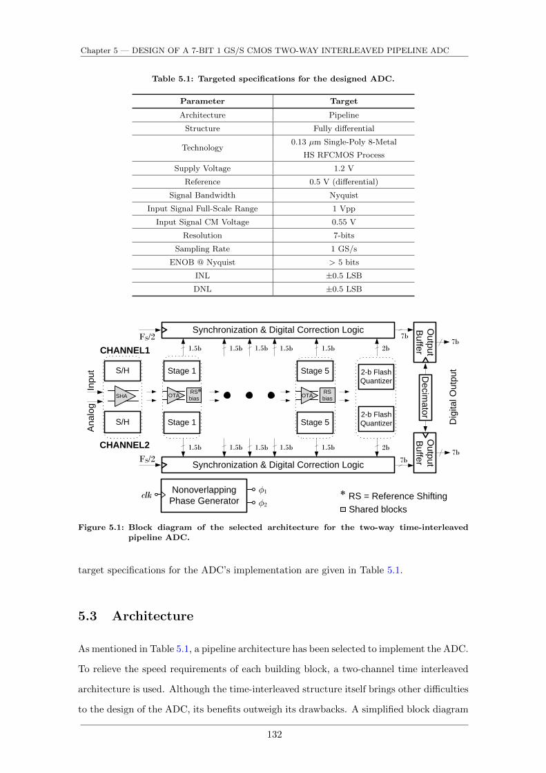
Chapter 5 — DESIGN OF A 7-BIT 1 GS/S CMOS TWO-WAY INTERLEAVED PIPELINE ADC
Table 5.1: Targeted specifications for the designed ADC.
Parameter Target
Architecture Pipeline
Structure Fully differential
Technology0.13 µm Single-Poly 8-Metal
HS RFCMOS Process
Supply Voltage 1.2 V
Reference 0.5 V (differential)
Signal Bandwidth Nyquist
Input Signal Full-Scale Range 1 Vpp
Input Signal CM Voltage 0.55 V
Resolution 7-bits
Sampling Rate 1 GS/s
ENOB @ Nyquist > 5 bits
INL ±0.5 LSB
DNL ±0.5 LSB
Stage 1
Stage 1
Synchronization & Digital Correction Logic
1.5b 1.5b 1.5b 1.5b 1.5b 2b
Synchronization & Digital Correction Logic
1.5b 1.5b 1.5b 1.5b 1.5b 2b
7b
7b
An
alo
g In
pu
t 2-b Flash
Quantizer
CHANNEL2
CHANNEL1
S/H
S/H
SHA
Stage 5
Stage 5
Nonoverlapping
Phase Generatorclk
OTARS
biasOTA
RS
bias
2-b Flash
Quantizer
*
* RS = Reference Shifting
FS/2
FS/2
Shared blocks
Dig
ita
l O
utp
ut
Ou
tpu
t
Bu
ffer
Ou
tpu
t
Bu
ffer
De
cim
ato
r
7b
7b
Á1
Á2
Figure 5.1: Block diagram of the selected architecture for the two-way time-interleavedpipeline ADC.
target specifications for the ADC’s implementation are given in Table 5.1.
5.3 Architecture
As mentioned in Table 5.1, a pipeline architecture has been selected to implement the ADC.
To relieve the speed requirements of each building block, a two-channel time interleaved
architecture is used. Although the time-interleaved structure itself brings other difficulties
to the design of the ADC, its benefits outweigh its drawbacks. A simplified block diagram
132

5.4 — IMPLEMENTATION DETAILS
C
VopVip
Von
+ -
- +VCM
C
VinS1
S2
S3
S4
1
1
2
2
1'
1'
2
2
Figure 5.2: Flip-around front-end sample-and-hold circuit.
of the overall architecture of the implemented ADC is shown in Fig. 5.1.
Concerning the analog part of the system, it is composed of a distributed front-end
sample-and-hold (S/H), followed by five 1.5-bit stages and final 2-bit stage. The S/H is
distributed to relax its specifications. Although time-interleaved timing mismatch issues
would be solved with a single S/H, designing one for 1 GS/s with Nyquist bandwidth
would consume a lot of power and would make the timing scheme more complex. The
S/H amplifier (SHA) is shared between channels to reduce power consumption. Each 1.5-
bit stage employs the proposed CMRS-MDAC and 1.5-bit flash quantizer. To reduce power
consumption, the amplifier (based on the design of the one proposed in Section 4.3), and
reference shifting biasing circuit are shared between channels. The final stage is composed
of a 2-bit flash quantizer which is based on the proposed architecture of Section 4.2. An
on-chip analog buffer is used to buffer the common-mode voltage (VCM ) of the ADC.
Regarding the digital part of the system, the stages’ output bits are synchronized and
digital correction logic is used to correct for any possible errors. At the output, a decimator
is used to reduce the rate at which the bits are outputted (given the high sampling rate) and
finally, output buffers hold and drive the output bits. A nonoverlapping phase generator
is used to produce the two main nonoverlapping clock signals with accurate phase shift.
5.4 Implementation Details
5.4.1 Sample-and-Hold
The architecture of the front-end sample-and-hold (S/H), as shown in Fig. 5.2, is based
on the flip-around structure [184]. Fig. 5.2 depicts the fully differential circuit with mul-
tiplexer switches (found at the amplifier’s input, S3), which are used to switch the shared
amplifier between channels. During the sampling phase, the input voltage is sampled on
133

Chapter 5 — DESIGN OF A 7-BIT 1 GS/S CMOS TWO-WAY INTERLEAVED PIPELINE ADC
Table 5.2: Switch sizes used in the S/H stage.
Switch Type Size W/L (µm/µm)
S1, S3 NMOS 6/0.12
S2, S4 NMOS 3/0.12
VSS
VDD
M1
M2a
M3a
M4
Vop Von
VCM2
Vin
M2b
M3b
Vip
VCM2
(47/0.18)
(32/0.16)
(32/0.16)
(32/0.5)
C1
C1
Vop
Von
VCM2
VCMO
C2
C2
2
2
2
1
1
1
C1
C1
VCMO
1
1
1
2
2
2
C1 = 150 fF
C2 = 50 fF
(a) (b)
Figure 5.3: Sample-and-hold amplifier: (a) Circuit. (b) Time-interleaved SC-CMFB circuit.Transistor sizes are given in µm.
the capacitors. During the hold phase, the capacitors are connected between the input
and output of the amplifier, and the output voltage becomes the sampled input voltage
minus an error, mostly due to finite gain and GBW of the opamp. All switches are made
of small NMOS transistors (sizes given in Table 5.2) controlled by a clock-bootstrapping
scheme, which allows achieving the necessary early phases (indicated in Fig. 5.2 by 1’) for
signal-independent sampling. This scheme is discussed further on in this chapter.
The capacitance value of the flip-around capacitors is 400 fF each. This value has been
chosen in order to set the ADC’s thermal noise power below half the ADC’s quantization
noise power.
The amplifier used in the S/H is a single-stage inverter-input self-biased OTA, as
depicted in Fig. 5.3a. Basically it is a single-stage version of the amplifier described in
Section 4.3. It is identical to the output stage of that amplifier, in the sense that it has
the same architecture, and the circuit is biased and the output CM level is controlled by
the common-mode voltage (VCM2) generated by the dedicated SC-CMFB circuit. This
time-interleaved SC-CMFB circuit has a fixed load (C2) and switched load (C1) as shown
in Fig. 5.3b. The sizes of the transistors and capacitance values are given in Fig. 5.3.
134

5.4 — IMPLEMENTATION DETAILS
103
106
109
−10
0
10
20
30
Frequency, Hz
Open
-loop
Gain,
dB
103
106
109
−100
−50
0
Frequency, Hz
Phase,de
g
Figure 5.4: Bode diagrams of the S/H amplifier overPVT corners.
Table 5.3: Key performance sum-mary of the S/H ampli-fier.
Parameter Value
Open-loop DC gain 26 dB
GBW† 3.7 GHz
Settling time†(0.1V step) 249 ps
Settling time†(1V step) 314 ps
Phase Margin† 90
Output Swing 1.3 V
Slew Rate 5400 V/µs
Total Input Offset 2.8 mV
Power @ 1.2 V 986 µW
† CL = 400 fF
Fig. 5.4 depicts the open-loop Bode diagrams of the amplifier over PVT corners1. Table 5.3
summarizes the simulated performance of this amplifier for the typical corner.
5.4.2 CMRS Multiplying-DAC
The MDAC architecture adopted for all stages of the implemented pipeline ADC was
the 1.5-bit CMRS-MDAC presented and previously discussed in Section 3.3. Given that
this MDAC circuit has already been fully detailed before, it will be the objective of this
section to outline the design of the implemented 1.5-bit pipeline stage, discussing its time-
interleaved operation with shared amplifier and shared reference shifting biasing (RS Bias)
circuit, and indicating the alterations made to the original MDAC circuit. The amplifier,
CMFB, and flash quantizer used in the stage will be discussed further on in this chapter.
The simplified block diagram of the implemented pipelined stage is shown in Fig. 5.5.
The only blocks of interest here are the RS Bias and MDAC blocks. Fig. 5.5 shows (shaded
in grey) the blocks shared between the channels, which are the RS Bias and the OTA.
First the MDAC then the RS Bias circuit will be discussed.
The unity feedback factor CMRS-MDAC circuit is repeated for convenience in Fig. 5.6a,
illustrating the alterations made to the original circuit (Fig. 3.5a). These changes basically
1Corners considered: tt, ss, and ff for process; 1.2 V±5% for supply voltage, and -40, 27, and 85
for temperature.
135

Chapter 5 — DESIGN OF A 7-BIT 1 GS/S CMOS TWO-WAY INTERLEAVED PIPELINE ADC
Vid
MDACCH1
X1Y1Z1
RS Bias
IP IN
MDACCH2
IP IN
X2Y2Z2
Vod
1.5b FQCH1
OTA
1.5b FQCH2
Shared blocks
Figure 5.5: 1.5-bit time-interleaved stage illustrating shared blocks (shown in grey).
consist of removing C3 and two switches, and adding switches S4 and S8. It should be
noticed that two switches still remained from the original compensation circuit, as they
were sufficient for parasitic compensation (using Cp61) at the 7-bit level. This type of
compensation is sufficient up to 8-bit accuracy, whereas for 9-bit accuracy (and above),
C3 and all switches (with adequate matching) should to be used. Switch S4 was added
as a multiplexer given that the amplifier is shared between channels and S8 was used to
short-circuit the amplifier’s inputs, destroying any residual charge, thus minimizing the
memory effect due to the amplifier’s input capacitance. φr is a very short pulse that is only
high between the ending of the sampling phase and the start of the residue amplification
phase (see Fig. 5.6b for an idea). Parasitic compensation was initiated at the design level
by balancing switch sizes, but careful layout and iterative parasitic extraction ultimately
dictated the process in which parasitic balancing was achieved. It is important to mention
that this process, and therefore, the parasitic-aware layout of this MDAC circuit became
quite intensive.
A timing diagram and the waveform of the output voltage of the MDAC are shown
in Fig. 5.6b, 5.6c, respectively. After signal independent sampling takes place, the main
capacitors of the MDAC are associated in series for the gain of two. This occurs, until the
flash quantizer has made its decision, and X, Y , or Z is fed to the MDAC. In the case of
X or Z, reference shifting occurs, which is illustrated in Fig. 5.6c for both modes. If too
much time is given to the quantizer, the output of the amplifier could increase to beyond
its output swing (because of the gain of two), driving its transistors into the triode region
causing distortion. In the implemented ADC the quantizer’s decision time was minimized,
which helps the amplifier stay in saturation and also less current is needed for reference
136
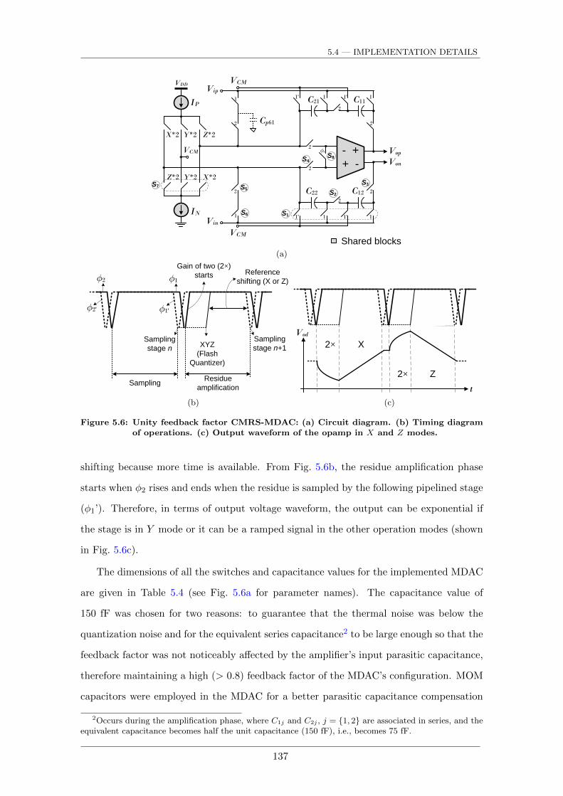
5.4 — IMPLEMENTATION DETAILS
C12
VCM
VDD
C11C212
2
1
Vip11
Vin
2
2
2
1 1
X*2 Y*2 Z*2
Z*2 Y*2 X*2
IN
IP1'
1'
Von
Vop- +
+ -
1'
1
2
1'
VCM
VCM
Cp61
2
2
S1
S2
S3
S4
S5
S6
S7
C22
Shared blocks
S8
Ár
(a)
Á1Á2
Á2'
Sampling
stage n
Sampling
stage n+1
Á1'
XYZ
(Flash
Quantizer)
Reference
shifting (X or Z)
Gain of two (2×)
starts
Residue
amplificationSampling
Vod
t
X2×
Z2×
(b) (c)
Figure 5.6: Unity feedback factor CMRS-MDAC: (a) Circuit diagram. (b) Timing diagramof operations. (c) Output waveform of the opamp in X and Z modes.
shifting because more time is available. From Fig. 5.6b, the residue amplification phase
starts when φ2 rises and ends when the residue is sampled by the following pipelined stage
(φ1’). Therefore, in terms of output voltage waveform, the output can be exponential if
the stage is in Y mode or it can be a ramped signal in the other operation modes (shown
in Fig. 5.6c).
The dimensions of all the switches and capacitance values for the implemented MDAC
are given in Table 5.4 (see Fig. 5.6a for parameter names). The capacitance value of
150 fF was chosen for two reasons: to guarantee that the thermal noise was below the
quantization noise and for the equivalent series capacitance2 to be large enough so that the
feedback factor was not noticeably affected by the amplifier’s input parasitic capacitance,
therefore maintaining a high (> 0.8) feedback factor of the MDAC’s configuration. MOM
capacitors were employed in the MDAC for a better parasitic capacitance compensation
2Occurs during the amplification phase, where C1j and C2j , j = 1, 2 are associated in series, and theequivalent capacitance becomes half the unit capacitance (150 fF), i.e., becomes 75 fF.
137

Chapter 5 — DESIGN OF A 7-BIT 1 GS/S CMOS TWO-WAY INTERLEAVED PIPELINE ADC
Table 5.4: Parameter values used in the MDACs. Switch widths are in µm (lengths of alltransistors are set to 0.12 µm).
Device Type Value
S1 NMOS 5
S2, S3 NMOS 1
S4 NMOS 0.64
S5 NMOS 0.32
S6 NMOS 0.64
S7 ATG† 0.64/1.15‡
S8 NMOS 2
All capacitors MOM 150 fF
† Asymmetrical transmission gate‡ NMOS/PMOS
VSS
VDD
Rcas Rboff-
chip
IP
IN
VCASN
VBN
VBP
VCASP
M1 M2
M3
M4
M5
M6
M7
M8
M9
M10
M13
M14
M11
M12
Cdecn
Cdecp
Figure 5.7: Reference shifting biasing circuit, including current mirrors and current sources.
and for reduced area (compared to MIM capacitors). As can be seen in Table 5.4, the
MDAC’s switches are all NMOS transistors because, similar to the S/H stage, all 1.5-bit
MDAC stages also employ a clock-bootstrapping scheme to control the stage’s switches
(discussion of this topic is given further on). This scheme also generates early phases
(indicated in Fig. 5.6a by 1’) for signal-independent sampling.
RS Bias
Regarding the RS Bias block of Fig. 5.5, as shown at transistor level in Fig. 5.7, it consists
of NMOS and PMOS cascoded current mirrors and current sources. The objective of this
circuit is to generate IP (for sourcing) and IN (for sinking). Given the prototype and
proof-of-concept nature of the implemented ADC, the currents for the current mirrors
were generated and controlled off-chip (through Rcas and Rb)3. Due to the high speed
3Notice that, in a future design of this ADC, as an intellectual propriety (IP) product, these two currentswould be generated on-chip either using an SC reference current generator [185] or using a replica MDACtogether with a servo-loop.
138

5.4 — IMPLEMENTATION DETAILS
operation of the ADC, the currents never turn off. They are always steered to one MDAC
or the other4 (because the MDACs operate in opposite phases), or in the situation where
the operation mode is Y , the current is steered from IP directly to IN (see Fig. 5.6a for
a better understanding). Given that the current sources connect to the amplifier’s inputs
in X and Z modes (for reference shifting), it is important that when the MDAC is in
Y mode, the node between IP and IN maintains a voltage close to the amplifier’s input
common-mode voltage. This is crucial to reduce recovery time when the MDAC goes into
X or Z mode again. To help minimize this problem, VCM is connected between the current
sources (in Y mode), therefore avoiding this node from floating and possibly drifting (refer
to Fig. 5.6a).
The dimensions of the transistors used in the RS Bias circuit are given in Table 5.5.
Table 5.5: Transistor dimensions of the RS Bias circuit.
Transistor Size W/L (µm/µm)
M1 3/1
M2, M4, M6, M8 7.92/0.2
M3, M5, M7, M9 16/0.17
M10 3/0.3
M11, M13 16/0.12
M12, M14 7.9/0.16
Decoupling capacitors (MOS capacitors)
Cdecn, Cdecp 200 fF
5.4.3 Flash Quantizer
1.5-bit Flash Quantizer
The flash quantizer architecture adopted for all 1.5-bit stages of the implemented ADC is
the one proposed and discussed in Section 4.2. Fig. 5.8 shows its circuit diagram, which
includes the sampling circuit, the D-FFs, the XYZ encoder, and the digital logic for timing
control of the various blocks. Recall, from Fig. 5.5, that each channel has its own flash
quantizer, no sharing of any part of this circuit is done.
The analog part of the flash quantizer with sampling circuit, which is responsible for
comparison, is shown in Fig. 5.8a. During the sampling phase (φ1), the input signal is
sampled on the CS capacitors (signal-independent sampling occurs) and, simultaneously,
the input signal is connected to the quantizer’s inputs, allowing it to initiate comparison.
4The RS Bias circuit is shared between channels to reduce power consumption and circuit overhead,and therefore provides current for reference shifting for both MDACs.
139

Chapter 5 — DESIGN OF A 7-BIT 1 GS/S CMOS TWO-WAY INTERLEAVED PIPELINE ADC
1
1
1'
Vip
Vin
VCMI
Vinp
Vinn
VSS
VDD
M5
MP1
MN1
MP2
MN2
MP3
MN3
Vop Von
M4A M4B
Vinp Vinn 2
1
VCMI
Cdecp
Cdecn
MP4
MN4
MP5
MN5S4
S5
S1
S2
S3CS
CS
(a)
Á = Á2D
Vop
VopL VopLÁÁ
ÁÁ
Á
Á
Á Á
Von
VonL VonLÁÁ
ÁÁ
Á
Á
(b)
Z
Y
VopLVonLÁ2XYZ
VonLVopLÁ2XYZ
Á1
Á1
Á1
X
XZ
Z
Y
X
(c)
XYZ
Á1' Á2D Á2XYZ
Á1 Á2
Comparison
time
Reference
shifting time
Á2
Á2D
Á2XYZ
(d)
Figure 5.8: Implemented 1.5-bit flash quantizer: (a) Circuit diagram of analog part withsampling circuit. (b) D-type flip-flops. (c) XYZ encoder. (d) Timing controland diagram of operations.
During the comparison/decision phase (φ2), only the held signal is connected to the quan-
tizer’s inputs, while the common-mode (CM) voltage of the input signal (node between
capacitors) is connected to the quantizer’s VCM input. Devices S4, S5, Cdecn and Cdecp
(MOS capacitors) have been added to hold the sampled signal’s CM voltage more constant
for the comparison/decision phase. This phase is divided into various sub-intervals (see
φ2 of Fig. 5.8d). First a certain amount of time is allocated for the quantizer to make a
140

5.4 — IMPLEMENTATION DETAILS
decision, after which the D-FFs open and the output of the quantizer is held. The circuit
adopted for the D-FFs is shown in Fig. 5.8b. The second sub-interval is for the XYZ
encoder (Fig. 5.8c), which takes the D-FF’s outputs and clock signals to make a final
decision on whether X, Y , or Z is high. This decision provides the MDAC with valid X,
Y , or Z signals for reference shifting. Therefore, these signals are at a low state during
the sampling phase, because the MDAC of the opposite channel will be in its residue am-
plification phase and could be using the RS Bias circuit (recall that the RS Bias circuit
is shared between channels). The timing control circuit and complete timing diagram of
operations are given in Fig. 5.8d.
The dimensions of the transistors, switches, and capacitances used in the analog part
of the flash quantizer are given in Table 5.6 for a threshold (switching) voltage of ±125 mV
(a full-scale input voltage of 1 Vpp has been specified).
Table 5.6: Dimensions and capacitances of the devices used in the implemented 1.5-bit flashquantizer for VTH = ±125 mV. Transistor dimensions are given in µm.
Device Type Value
MP1, MP2 PMOS 13/0.15
MP3 PMOS 4/0.24
M5 PMOS 30/0.24
MP4, MP5 PMOS 1.2/0.12
MN1, MN2 NMOS 10/0.16
MN3 NMOS 8.5/0.16
M4A NMOS 5.5/2
M4B NMOS 1.7/2
MN4, MN5 NMOS 0.32/0.12
S1, S2, S3 NMOS 2.5/0.12
S4, S5 NMOS 5/0.12
CS MOM 50 fF
Cdecn, Cdecp MOS 50 fF
2-bit Flash Quantizer
The last stage of the implemented pipeline ADC is a 2-bit flash quantizer. The architecture
employed is also similar to the 1.5-bit quantizer described in Section 4.2, with the exception
that this one was sized for threshold voltages of ±250 mV, and a simplified version of the
1.5-bit quantizer was adopted for the 0 V threshold level. The latter is depicted in Fig. 5.9.
Regarding the circuit of the ±250 mV flash quantizer and comparing it with the one
shown in Fig. 5.8a, switches S4, S5, and both decoupling capacitors have been removed,
as they were not critical here. Two load capacitors have been added, one between Vip
141

Chapter 5 — DESIGN OF A 7-BIT 1 GS/S CMOS TWO-WAY INTERLEAVED PIPELINE ADC
VSS
VDD
M5
MP1
MN1
MP2
MN2
Vo
M4A M4B
Vinp
MP3
MN3
Vinn
Figure 5.9: Implemented comparator used for VTH = 0 V.
and VCMI , and the other between Vin and VCMI . These capacitors act as a load for
the stability of the residue amplifier of the previous pipelined stage, given that the last
pipelined stage does not have an MDAC circuit. Regarding the 0 V threshold quantizer
(Fig. 5.9), which is in fact just a comparator (only one output is necessary), the VCM input
has been replaced with a signal input and one of the signal inverters has been removed.
One of the outputs controls the biasing of the circuit, while the other is the desired output
signal. This circuit is very similar to the one proposed in [138]. The analog part of the
2-bit quantizer is followed by three D-FFs, similar to the ones shown in Fig. 5.8b, and a
2-bit encoder, that generates the two least significant bits of the ADC. The dimensions
of the transistors, switches, and capacitances used in the analog part of the 2-bit flash
quantizer are given in Table 5.7 for the threshold levels of ±250 mV (see Fig. 5.8a for
component names) and 0 V (Fig. 5.9).
5.4.4 Opamp and CMFB
The architecture of the amplifier adopted for all MDAC stages is identical to the one pro-
posed and discussed in Section 4.3. This inverter-based self-biased amplifier was employed
given its high speed at low power consumption, i.e., its high energy efficiency. Given that
no structural changes were made to the original amplifier and CMFB circuits, no circuit
diagram will be shown here. The sizes of the transistors and capacitance values used in
the amplifier and CMFB circuits are given in Table 5.8. Refer to Fig. 4.12 and Fig. 4.13
for device names. The architecture used for SC-CMFB, CMFB2, is identical to that used
142

5.4 — IMPLEMENTATION DETAILS
Table 5.7: Dimensions and capacitances of the devices used in the implemented 2-bit flashquantizer for VTH = ±250 mV and VTH = 0 V. Transistor dimensions are given inµm.
Device Type Value
S1, S2, S3 NMOS 5/0.12
CS MOM 100 fF
CL MOM 100 fF
VTH = ±250 mV
MP1, MP2 PMOS 9/0.12
MP3 PMOS 60/0.12
M5 PMOS 30/0.24
MP4, MP5 PMOS 0.58/0.12
MN1, MN2 NMOS 60/0.12
MN3 NMOS 4/0.36
M4A NMOS 6.5/1
M4B NMOS 26/1
MN4, MN5 NMOS 0.16/0.12
VTH = 0 V
MP1, MP2 PMOS 10/0.14
M5 PMOS 14/0.24
MP3 PMOS 0.58/0.12
MN1, MN2 NMOS 10/0.14
M4A NMOS 3.3/1
M4B NMOS 3.5/1
MN3 NMOS 0.16/0.12
in the amplifier of the S/H stage (see Fig. 5.3b) given that this amplifier is also shared
between channels.
Table 5.8: Transistor dimensions and capacitance values used in the implemented amplifierand CMFB circuits. Transistor dimensions are given in µm.
Device Type Value
M11 PMOS 7.94/0.28
M12a, M12b PMOS 10.72/0.12
M13a, M13b NMOS 8.56/0.12
M14a, M14b NMOS 3/0.95
M21 PMOS 71.44/0.38
M22a, M22b PMOS 36.28/0.14
M23a, M23b NMOS 20/0.15
M24 NMOS 64/1.16
M31 PMOS 16.82/0.14
M32 NMOS 15.84/0.13
M33 PMOS 17.92/0.13
M34 NMOS 8.68/0.13
CCa, CCb MOM 90 fF
CCM MOM 120 fF
CMFB2
C1 MOM 90 fF
C2 MOM 250 fF
All switches NMOS 1/0.12
Fig. 5.10 depicts the open-loop Bode diagrams of the amplifier over PVT corners.
Table 5.9 summarizes the simulated performance of this amplifier for the typical corner.
143

Chapter 5 — DESIGN OF A 7-BIT 1 GS/S CMOS TWO-WAY INTERLEAVED PIPELINE ADC
103
106
109
0
20
40
Frequency, Hz
Open
-loop
Gain,
dB
103
106
109
−150
−100
−50
0
Frequency, Hz
Phase,de
g
Figure 5.10: Bode diagrams of the MDAC amplifierover PVT corners.
Table 5.9: Key performance sum-mary of the amplifier usedin the MDACs.
Parameter Value
Open-loop DC gain 45 dB
GBW† 2.3 GHz
Settling time†(0.1V step) 511 ps
Settling time†(1V step) 736 ps
Phase Margin† 57
Output Swing 1.4 V
Slew Rate 3400 V/µs
Total Input Offset 4.1 mV
Power @ 1.2 V 1.18 mW
† CL = 600 fF
5.4.5 Switches and Clock-Bootstrapping Circuits
As already mentioned before and shown in the tables that indicate information about the
switches used in the various blocks discussed until now, most switches are simply NMOS
transistors. In a pipelined stage, the only switches that are not NMOS-only are those
used to steer the current for reference shifting in the MDAC circuits, which are ATGs
(asymmetrical transmission gates) controlled by the X, Y , and Z phases. Using small
NMOS-only switches is made possible by driving all switches with bootstrapped voltages.
A block diagram of the scheme that makes this possible is shown in Fig. 5.11a, accompanied
by a timing diagram given in Fig. 5.11b. The main clock generator (described in the next
section) generates two nonoverlapping clock phases, φ1 and φ2. Both phases are connected
to each stage, where they are regenerated and bootstrapped phases are produced to be
used by all blocks in the stage. The block diagram of Fig. 5.11a only depicts the blocks
used for one main phase. Therefore, each stage has two of these blocks. Circuit operation
is as follows: the three inverters regenerate and delay the original main phase (φ). This
phase and its inverted counterpart (φn) connect to one clock-bootstrapping circuit, which
is responsible for creating the early phase, φBe (‘B’ for bootstrapped and ‘e’ for early). The
remaining inverters are used to delay φ even more, creating φd and φdn. These connect to
the other bootstrapping circuit, which creates φB. The delay between φ and φd is sufficient
144
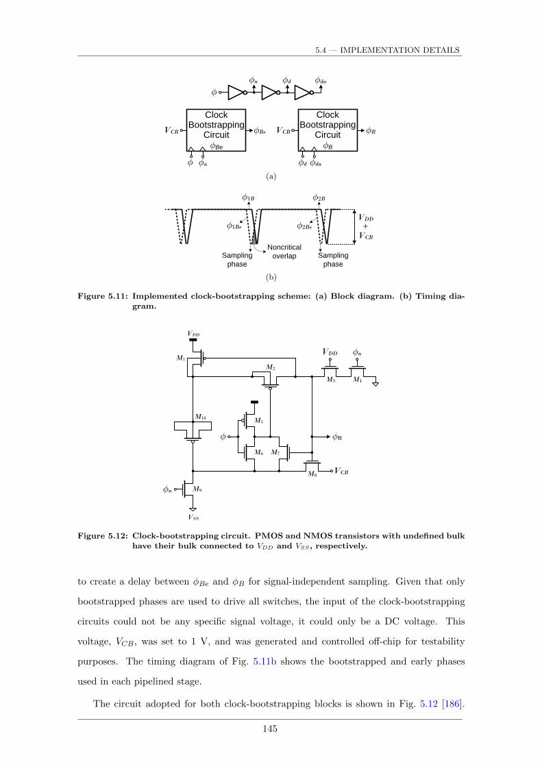
5.4 — IMPLEMENTATION DETAILS
ClockBootstrapping
CircuitÁBe
VCB ÁBe
Á Án
Á
Ád ÁdnÁn
ClockBootstrapping
CircuitÁB
VCB ÁB
Ád Ádn
(a)
Á1B
Noncritical
overlap
Á2B
Á1Be Á2Be
Sampling
phase
Sampling
phase
VDD+VCB
(b)
Figure 5.11: Implemented clock-bootstrapping scheme: (a) Block diagram. (b) Timing dia-gram.
VSS
VDD
VCB
Á
Án
ÁB
ÁnVDDM1
M3 M4
M2
M5
M6 M7
M8
M9
M10
Figure 5.12: Clock-bootstrapping circuit. PMOS and NMOS transistors with undefined bulkhave their bulk connected to VDD and VSS, respectively.
to create a delay between φBe and φB for signal-independent sampling. Given that only
bootstrapped phases are used to drive all switches, the input of the clock-bootstrapping
circuits could not be any specific signal voltage, it could only be a DC voltage. This
voltage, VCB, was set to 1 V, and was generated and controlled off-chip for testability
purposes. The timing diagram of Fig. 5.11b shows the bootstrapped and early phases
used in each pipelined stage.
The circuit adopted for both clock-bootstrapping blocks is shown in Fig. 5.12 [186].
145

Chapter 5 — DESIGN OF A 7-BIT 1 GS/S CMOS TWO-WAY INTERLEAVED PIPELINE ADC
0 0.5 1 1.5 20
1
2
Time, ns
φ,V
φB
φBe
(a)
2.05 2.1 2.15 2.2 2.25 2.30
1
2
Time, ns
φ,V
φ1Be
φ1B φ2Be
φ2B
(b)
Figure 5.13: (a) Simulated timing diagram of the clock-bootstrapping circuits’ outputs. (b)Zoom of the timing diagram.
Given that each bootstrapping circuit drives a different number of switches, hence a dif-
ferent capacitive load, they have different transistor sizings, which are given in Table 5.10.
Fig. 5.13 depicts the simulated result of each clock-bootstrapping circuit, illustrating the
nonoverlapping, rise and fall times, and the noncritical overlap.
Table 5.10: Transistor dimensions used in the implemented clock-bootstrapping circuits. Di-mensions are given in µm.
Transistor Size
Clock-bootstrapping circuit φBM1, M5 20/0.12
M2 30/0.12
M3, M4, M8 14/0.12
M6, M7 5/0.12
M9 7/0.12
M10 10/10
Clock-bootstrapping circuit φBeM1, M5 12/0.12
M2 16/0.12
M3, M4, M8 12/0.12
M6, M7 3/0.12
M9 6/0.12
M10 9/9
146
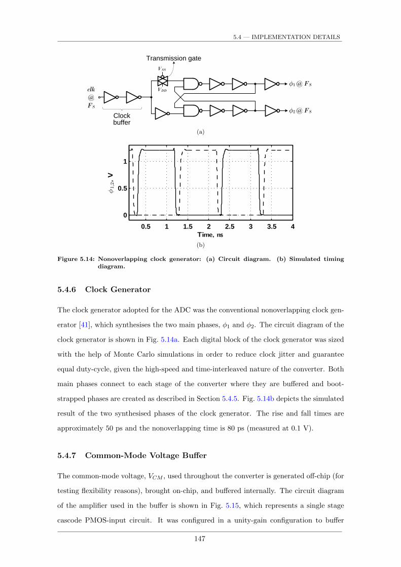
5.4 — IMPLEMENTATION DETAILS
clk
@
FS
VDD
VSS
Á1 @ FS
Clock buffer
Transmission gate
Á2 @ FS
(a)
0.5 1 1.5 2 2.5 3 3.5 4
0
0.5
1
Time, ns
φ1,2,V
(b)
Figure 5.14: Nonoverlapping clock generator: (a) Circuit diagram. (b) Simulated timingdiagram.
5.4.6 Clock Generator
The clock generator adopted for the ADC was the conventional nonoverlapping clock gen-
erator [41], which synthesises the two main phases, φ1 and φ2. The circuit diagram of the
clock generator is shown in Fig. 5.14a. Each digital block of the clock generator was sized
with the help of Monte Carlo simulations in order to reduce clock jitter and guarantee
equal duty-cycle, given the high-speed and time-interleaved nature of the converter. Both
main phases connect to each stage of the converter where they are buffered and boot-
strapped phases are created as described in Section 5.4.5. Fig. 5.14b depicts the simulated
result of the two synthesised phases of the clock generator. The rise and fall times are
approximately 50 ps and the nonoverlapping time is 80 ps (measured at 0.1 V).
5.4.7 Common-Mode Voltage Buffer
The common-mode voltage, VCM , used throughout the converter is generated off-chip (for
testing flexibility reasons), brought on-chip, and buffered internally. The circuit diagram
of the amplifier used in the buffer is shown in Fig. 5.15, which represents a single stage
cascode PMOS-input circuit. It was configured in a unity-gain configuration to buffer
147

Chapter 5 — DESIGN OF A 7-BIT 1 GS/S CMOS TWO-WAY INTERLEAVED PIPELINE ADC
VDDVDD
Rbias
off-
chip
Vi
Vout
(40/0.12) (40/0.12)
(15/2)
(320/0.12)
(240/0.12)
(48/0.12)
(48/0.12)
VSS
VSS
1 : 8M1
M2bM2a
M3b
M4b
M3a
M4a
Mb1Mb2
Mb3
Figure 5.15: Circuit diagram of the amplifier used to buffer VCM .
VCM . In order to limit the amplifier’s output noise and stabilize its output voltage (due
to the periodic clocking), the amplifier was loaded with a decoupling capacitor composed
of two MOS capacitors (one PMOS capacitor and one NMOS capacitor) with a total
capacitance of, approximately, 100 pF.
Table 5.11 summarizes the electrically simulated performance of this amplifier.
Table 5.11: Performance summary of the on-chip common-mode voltage buffer.
Parameter Value
Open-loop DC gain 20 dB
GBW† 25 MHz
Phase margin (PM)† 95
Total Input offset 9 mV
Power @ 1.2 V 1.5 mW
Fixed load (filter) 100 pF
† CL = 100 pF
Notice that this buffer has been sized targeting the maximum conversion rate of 1 GS/s
and its power dissipation does not scale with the clock frequency. Again, in a future
redesign of this ADC as an IP, an on-chip SC current reference generator would also be
integrated and Rbias would not be required.
5.4.8 Digital Backend
The digital backend of the converter is primarily composed of synchronization logic, digital
correction logic, and digital output buffers. Given the high speed nature of the converter,
two protective measures were adopted for acquiring the output bits. One measure em-
ployed two random access memories (RAMs), one for each channel, where the output bits
148
5.4 — IMPLEMENTATION DETAILS
are written to the RAM at full clock speed and then brought off-chip at a much lower fre-
quency. The second measure consisted of a time-interleaved decimator, where the output
buffer is clocked at a lower rate (decimated rate) and the bits are brought off-chip at this
lower frequency. Two measures were necessary because the RAM was synthesized and
added to the final layout by another group5, and it was the first time a time-interleaved
decimator was been implemented in an ADC design (in our research group). A digital
input, SEL, was used to switch between both modes. The decimator will be discussed in
the following section, and no more references to the RAM will be made, since it was not
found necessary during testing.
As already explained in the introductory chapter of this thesis, the digital outputs of
each stage (Y and Z) need to be synchronized before digital correction. The synchro-
nization logic block diagram is depicted in Fig. 5.16a. This circuit is composed of shift
registers, which consist of D-FFs, and delay and buffering logic. All inputs connect to
their respective D-FFs and the final outputs connect directly to the correction logic. The
input clock is generated by the flash quantizer of the first MDAC stage (of the pipeline).
This allows the synchronization logic to know when the bits, of each stage, are ready to
be saved (clocked).
As mentioned, the output bits when time-aligned, are connected to the correction logic.
This circuit is composed of a serial sequence of 1-bit full adders which produce the final
(and corrected) digital outputs. The block diagram of this circuit is shown in Fig. 5.16b.
Finally, the outputs from the correction logic are fed to the output buffer circuit.
Here the bits are held using a bank of D-FFs followed by two cascaded inverters for
buffering. The input clock to this circuit is generated and controlled by the decimator. If
the decimator is selected to be used, a lower frequency clock is generated and fed to the
digital output block. In this way the circuit is clocked at a lower frequency, hence the
decimation effect. If the RAM is selected, the buffer circuit is clocked at full speed, and
the bits are written to the RAM.
Due to time-interleaving, two of each of the above mentioned circuits, except for the
decimator, had to be employed.
5IMEC, the contact through the Europractice program.
149

Chapter 5 — DESIGN OF A 7-BIT 1 GS/S CMOS TWO-WAY INTERLEAVED PIPELINE ADC
D Q
Q
D Q
Q
D Q
Q
D Q
Q
D Q
Q
D Q
Q
D Q
Q
D Q
Q
D Q
Q
D Q
Q
D Q
Q
D Q
Q
D Q
Q
D Q
Q
D Q
Q
D Q
Q
D Q
Q
D Q
Q
D Q
Q
D Q
Q
D Q
Q
D Q
Q
D Q
Q
D Q
Q
D Q
Q
D Q
Q
D Q
Q
D Q
Q
D Q
Q
D Q
Q
DelayÁin
Á Án
Án
Á Á Á
Á Á Á
Á Á
Á Á
Á
Á
Án
Án
Án
Án
Án
Án
Án
Án
Án
Án
Án
Án Án
ÁnÁn
Án
Án
Y1
Z1
Y2
Z2
Y3
Z3
Y4
Z4
Y5
Z5
Y6
Z6
Y1s
Z1s
Y2s
Z2s
Y3s
Z3s
Y4s
Z4s
Y5s
Z5s
Y6s
Z6s
DelayY6s b0
1-bit
Full Adder
AB
CiSCoY5s
Z6s
1-bit
Full Adder
AB
CiSCoY4s
Z5s
1-bit
Full Adder
AB
CiSCoY3s
Z4s
1-bit
Full Adder
AB
CiSCoY2s
Z3s
1-bit
Full Adder
AB
CiSCoY1s
Z2s
1-bit
Full Adder
AB
CiS
Z1s
b1
b2
b3
b4
b5
b6
(a) (b)
Figure 5.16: Digital backend: (a) Synchronization. (b) Correction logic.
5.4.9 Decimator
The high speed nature of the implemented converter demanded for a decimator at the
output to reduce the rate at which the bits are outputted, therefore facilitating data
acquisition through external measurement equipments. This section describes the imple-
mented time-interleaved decimator. The objective of this circuit is to discard samples but
in a time-interleaved way, i.e., acquire a sample from one channel, then discard samples,
then acquire a sample from the other channel, then discard samples, after which the pro-
cess repeats itself. A time-interleaved decimator had to be implemented because using
one conventional decimator [187] per channel, causes the equivalent to a timing mismatch
error in the output FFT. In other words, when the outputs of each channel (separately
150

5.4 — IMPLEMENTATION DETAILS
4-bit
Counter
RSTD0
D1
D2
D3
D Q
Q
D Q
Q
Á1
Á1
Á2
0111
0000
RST
Á1_pulse
Á2_pulse
Figure 5.17: Block diagram of the time-interleaved decimator.
J Q
QK
RST
J Q
QK
RST
J Q
QK
RST
J Q
QK
RST
VDD
Á1 Á1 Á1 Á1
RST
D0D1 D2 D3
JK-DET
(a)
J
K Á1
RST
D-DET
D Q
QRST
QÁÁ
ÁÁ
Á
Á Q
RST
D
Á1
Á Á
D Flip-FlopSynchronous reset
Dual edge triggering circuit
(b) (c)
Figure 5.18: Circuit diagrams of: (a) 4-bit counter. (b) JK-FF with synchronous reset. (c)D-FF with dual edge triggering circuit with synchronous reset.
decimated) are interleaved for post-processing, a timing error occurs, with a similar effect
in the FFT to a timing mismatch error of time-interleaved ADCs.
The time-interleaved decimator, as described by its block diagram in Fig. 5.17, is
composed of a 4-bit counter, and logic to control the reset and clock signals. The reset
signal is used to restart the counter, while the clock signals (φi pulse) are used to clock the
digital output buffers with a lower frequency clock. In order to synchronize the output
clock signals with the rest of the circuit’s clocking, two D-FFs are used. The counter
circuit diagram is shown in Fig. 5.18a, which is composed of four cascaded JK flip-flops
(JK-FF). Besides counting, this circuit also serves to divide the main clock (φ1 was used)
frequency by 16, which is then sent off-chip to synchronize the logic analyzer for data
151

Chapter 5 — DESIGN OF A 7-BIT 1 GS/S CMOS TWO-WAY INTERLEAVED PIPELINE ADC
capture (D3 of Fig. 5.18a was used). The implemented converter has two channels, which
means that a digital word is outputted every edge of φ1, i.e., when φ1 falls, a digital word
from channel 1 is ready, when φ1 rises, coinciding with φ2 falling, a digital word from
channel 2 is ready. Therefore, the JK-FFs need to count both falling and rising edges of
φ1, and to this end, dual edge triggered (DET) JK-FFs have been used, as depicted in
Fig. 5.18b. In the composition of a JK-FF is a D-FF with synchronous reset, as shown
in Fig. 5.18c. The circuit that allows the dual edge triggering is illustrated in Fig. 5.18c
[188].
To sum up the decimator’s operation: it counts 14 edges (rising and falling) of φ1
and on the 15th clock edge, it signals the output buffer of channel 1 to hold the digital
word at its input. The decimator is then reset and after 14 counts it signals the output
buffer of channel 2 to hold the next digital word. The decimation factor is 15, which is an
odd number because an even number would cause the decimator to constantly clock the
same channel. Therefore, the decimator ‘ping-pongs’ between channels. When the output
samples are time-interleaved during the post-processing stage (FFT, etc.), they will be in
the correct order, and coherent sampling will not have been lost, nor timing errors will
appear in the FFT.
5.4.10 Complete ADC
To finalize this chapter, the dynamic performance of the complete ADC is evaluated.
An electrically simulated 4096-point FFT of the 7-bit ADC operating at 1 GS/s with
a -1 dBFS 20 MHz input signal (for typical conditions) is shown in Fig 5.19. The ADC
obtains a SFDR of 47.8 dB and an SNDR of 39 dB, which leads to a 6.2 bit ENOB. At this
sampling frequency, the total reference shifting current per stage is 68 µA and the total
power consumption of the ADC is 19.5 mW, which results in a FoM of 265 fJ/conv.-step.
152
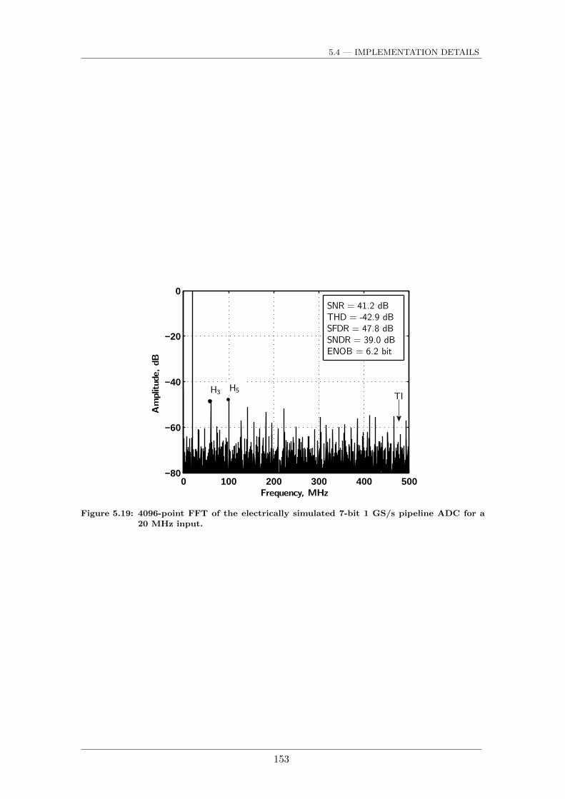
5.4 — IMPLEMENTATION DETAILS
0 100 200 300 400 500−80
−60
−40
−20
0
Frequency, MHz
Amplitud
e,dB
H3 H5TI
SNR = 41.2 dBTHD = -42.9 dBSFDR = 47.8 dBSNDR = 39.0 dBENOB = 6.2 bit
Figure 5.19: 4096-point FFT of the electrically simulated 7-bit 1 GS/s pipeline ADC for a20 MHz input.
153

Chapter 5 — DESIGN OF A 7-BIT 1 GS/S CMOS TWO-WAY INTERLEAVED PIPELINE ADC
154

Chapter 6
Integrated Prototypes andExperimental Results
6.1 Overview
This chapter discusses the implementation of two integrated circuit (IC) prototypes with
the objective of evaluating their performance and functionality. The first circuit concerns
the two-stage inverter-based self-biased amplifier presented and described in Section 4.3.
The second prototype concerns the 7-bit 1 GS/s two-way interleaved pipeline ADC, which
was presented in Chapter 5. For each prototype, a floorplan and layout will be shown,
and some design and layout considerations will be given. Equally, the designed printed
circuit board (PCB) and the respective test setup used for each circuit evaluation will be
presented. Each IC prototype section will end with the experimental results achieved and
a comparison will be carried out with the state-of-the-art.
Regarding the technology employed to design and implement the circuits, a standard
digital 0.13 µm 1.2 V 1P-8M CMOS process has been used. No special device options
such as, low- or high-VT , twin- or triple-well or low leakage devices, etc., were used. For
capacitors, the technology’s Metal-Insulator-Metal (MIM) capacitors, MOS capacitors,
and our design group’s proprietary Metal-Oxide-Metal (MOM) capacitors were used.
6.2 Two-Stage Inverter-Based Self-Biased Amplifier
To validate the theoretical results derived in Section 4.3, an optimization using the tech-
nique also described in the referred section, was carried out. The DM settling time at
155

Chapter 6 — INTEGRATED PROTOTYPES AND EXPERIMENTAL RESULTS
0.024 % error (12-bit accuracy) was set to 150 ns for a capacitive load of 4 pF. Due to
thermal noise constraints related with the target application, the minimum value for CC
was set to 0.5 pF. No common-mode (CM) settings were defined, the OS was maximized,
the power dissipation minimized, and the amplifier was optimized to provide stability for
closed-loop gains higher than 2. The CM voltage of the input signal and VCMO were
set to 550 mV. The value of VCMO is obtained by taking half the lowest supply voltage
(considering ±10 % variations), i.e., VCMO ≈ 0.9× VDD/2.
Table 6.1 summarizes the device sizing of the implemented amplifier (see Fig. 4.12 for
device names). All capacitors were implemented using MIM capacitors and the resistors
(for the CMFB circuit) were implemented with nonsalicide P+ poly resistors (readily
available, as a standard option, from the technology).
Table 6.1: Transistor dimensions, and capacitor and resistor values used in the implementedamplifier and CMFB circuits. Transistor dimensions are given in µm.
Device Type Value
M11 PMOS 209/5.2
M12a, M12b PMOS 225/1.6
M13a, M13b NMOS 50.9/0.9
M14a, M14b NMOS 22.8/0.3
M21 PMOS 62.9/8.6
M22a, M22b PMOS 80.4/0.7
M23a, M23b NMOS 194/1.2
M24 NMOS 12.6/1.7
M31 PMOS 103/1.5
M32 NMOS 5.4/1.4
M33 PMOS 103/1.5
M34 NMOS 5.4/1.4
CCa, CCb MIM 510 fF
CCM MIM 510 fF
CMFB
CCMFB MIM 100 fF
RCMFBNonsalicide P+ Poly
Resistor50 kΩ
6.2.1 Floorplan and Layout
Fig. 6.1 shows the floorplan, the layout, and the chip photograph of the implemented
amplifier. Fig. 6.1c highlights the amplifier core, the on-chip continuous time CMFB
circuit, the compensation capacitors CC , and the CM stabilization capacitor CCM (half
on each side of the amplifier). The total area occupied by the amplifier, with compensation
capacitors and CMFB, is 179×69 µm2. To facilitate the measurement stage of our design a
continuous time CMFB circuit was implemented. This on-chip CMFB substitutes the SC-
156

6.2 — TWO-STAGE INVERTER-BASED SELF-BIASED AMPLIFIER
Vin
Pad
CMFB
CMFB
CCM CCM
CC CC
PMOS
NMOS
VDD
PadVip
Pad
Von
PadVSS
PadVop
Pad
VCMO
Pad
Powerrings
Guardrings
(a)
(b) (c)
Figure 6.1: Implementation of the two-stage inverter-based self-biased amplifier: (a) Floor-plan. (b) Layout. (c) Chip photograph.
CMFB2 circuit of Fig. 4.13a, but has the same purpose and consists of a 100 fF capacitor
in parallel with a 50 kΩ resistor loading each output, connected at a common voltage,
which represents VCM2 (see Fig. 6.3a for an idea). Due to this resistance value, the CMFB
circuit slightly reduced the amplifier’s DC gain.
6.2.2 Design Considerations
It will be the objective here to briefly describe some considerations taken during the
design and layout of the amplifier. As can be seen in the amplifier’s floorplan, its core
was separated from the rest of the circuit by means of an n-well guard ring. This is not
mandatory because the circuit is entirely analog, nevertheless it is good practice.
Given that the input signals, Vip and Vin, and the common-mode voltage, VCMO, are
connected directly to the gates of the transistors, special precautions had to be taken.
This was necessary to avoid electrostatic discharge (ESD) issues. These discharges can
157
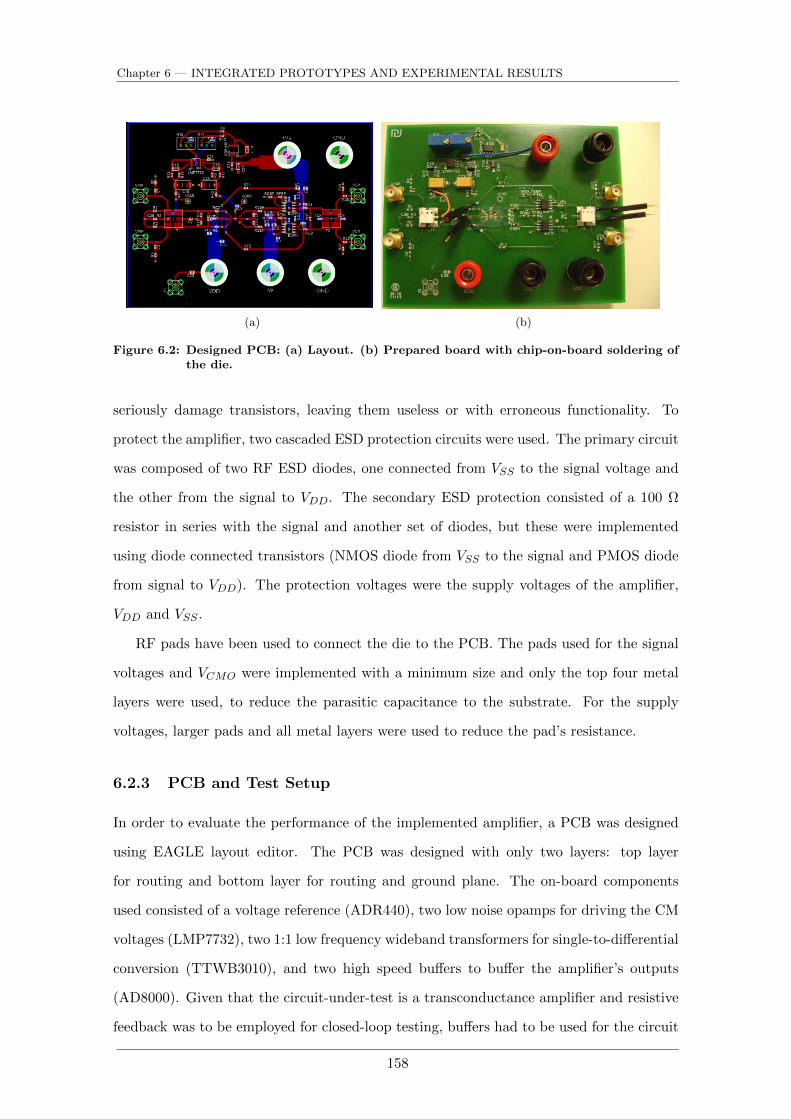
Chapter 6 — INTEGRATED PROTOTYPES AND EXPERIMENTAL RESULTS
(a) (b)
Figure 6.2: Designed PCB: (a) Layout. (b) Prepared board with chip-on-board soldering ofthe die.
seriously damage transistors, leaving them useless or with erroneous functionality. To
protect the amplifier, two cascaded ESD protection circuits were used. The primary circuit
was composed of two RF ESD diodes, one connected from VSS to the signal voltage and
the other from the signal to VDD. The secondary ESD protection consisted of a 100 Ω
resistor in series with the signal and another set of diodes, but these were implemented
using diode connected transistors (NMOS diode from VSS to the signal and PMOS diode
from signal to VDD). The protection voltages were the supply voltages of the amplifier,
VDD and VSS .
RF pads have been used to connect the die to the PCB. The pads used for the signal
voltages and VCMO were implemented with a minimum size and only the top four metal
layers were used, to reduce the parasitic capacitance to the substrate. For the supply
voltages, larger pads and all metal layers were used to reduce the pad’s resistance.
6.2.3 PCB and Test Setup
In order to evaluate the performance of the implemented amplifier, a PCB was designed
using EAGLE layout editor. The PCB was designed with only two layers: top layer
for routing and bottom layer for routing and ground plane. The on-board components
used consisted of a voltage reference (ADR440), two low noise opamps for driving the CM
voltages (LMP7732), two 1:1 low frequency wideband transformers for single-to-differential
conversion (TTWB3010), and two high speed buffers to buffer the amplifier’s outputs
(AD8000). Given that the circuit-under-test is a transconductance amplifier and resistive
feedback was to be employed for closed-loop testing, buffers had to be used for the circuit
158

6.2 — TWO-STAGE INVERTER-BASED SELF-BIASED AMPLIFIER
+-
Rg1
Rg2
Rf1
Rf2
ESD
ESD
ESD
ESD
VCMO
Integrated
circuit
+ -
VDD
ESD
VSS
1
1
Vop
Von
Vip
Vin
VipOA
VinOA
CMFB
(a)
Tektronix
1103
HP
4591A
S R T
Closed-loop
test setup
Tektronix
P6247
(b)
Closed-loop
test setup
TektronixTDS3052
Tektronix
1103
Tektronix
P6247
TektronixAWG 5102
(c)
Rohde&Schwarz
FSV
Closed-loop
test setup
(d)
Figure 6.3: Test setups for the amplifier evaluation: (a) Closed-loop circuit diagram. Setupsfor (b) open-loop frequency response, (c) step response, and (d) output noisemeasurement.
to maintain its DC gain. This situation introduced a new issue, which was the stability
of the complete closed-loop circuit composed of implemented amplifier and buffers. To
maintain stability and not affect the measurements of the proposed amplifier, the buffers’
closed-loop poles had to be at least ten times higher than the unity-gain frequency of
the implemented amplifier. Therefore the AD8000 buffers with a 1.5 GHz bandwidth
were used. Fig. 6.2 illustrates the designed PCB, and the prepared board with soldered
components and chip-on-board preparation of the die.
The test setup used to characterize the performance of the amplifier is shown in Fig. 6.3.
This setup was adapted from a Texas Instruments fully differential amplifier THS4521D
evaluation module [189]. In Fig. 6.3a a circuit diagram of the amplifier in closed-loop form
is shown. For resistors Rf1,2 and Rg1,2 a value of 100 Ω was used. Fig. 6.3b shows the
setup used to obtain the Bode diagrams (magnitude and phase) of the open-loop gain.
The step response of the amplifier was evaluated with the setup of Fig. 6.3c, and finally,
Fig. 6.3d shows how the output noise was measured.
159

Chapter 6 — INTEGRATED PROTOTYPES AND EXPERIMENTAL RESULTS
Gain
Phase
Figure 6.4: Amplifier’s open-loop magnitude and phase Bode diagrams.
The test equipment used to measure the frequency response, the time response, and
the noise is given below:
• HP 4195A Network Analyser: frequency response;
• Tektronix AWG510: generate input signals for step response;
• Tektronix TDS3052 Oscilloscope: observe output signals from step response;
• Rohde&Schwarz FSV Signal Analyser: noise measurements;
• Tektronix P6247 Differential Active Probe (and Tektronix 1103 Probe Power Sup-
ply): probe differential signals;
• Agilent 6624A DC Power Supply.
6.2.4 Experimental Results
Following the test setups described in the previous section, the amplifier’s frequency re-
sponse, step response, and noise were characterized. The measured open-loop magnitude
and phase Bode diagrams of the amplifier are shown in Fig. 6.4. For these measurements
the amplifier was in unity gain configuration and the active probe was connected to the
amplifier’s inputs (VipOA and VinOA). The AC response was then measured between the
output of the setup and the amplifier’s inputs (Vod/(VipOA − VinOA)). Due to this setup,
the amplifier’s inputs were loaded with an extra 200 kΩ || 1.0 pF impedance, while the
160

6.2 — TWO-STAGE INVERTER-BASED SELF-BIASED AMPLIFIER
(a)
(b)
Figure 6.5: Step responses: (a) Small-signal. (b) Large signal.
amplifier’s outputs were loaded with the RF pad, the PCB trace (parasitic capacitance
much larger than initially anticipated) and the input impedance of the AD8000 (≈ 2 MΩ
|| 3.6 pF). This extra loading degraded the AC response, especially the PM and the unity
gain frequency, which were measured to be less than 45 and 30.4 MHz, respectively. The
GBW was extrapolated to be around 35 MHz. Regarding the low frequency (DC) gain
of the amplifier, over 71 dB was measured, as indicated in Fig. 6.4. The large gain of
the amplifier made it even more difficult to measure, which explains the inaccuracy of
Fig. 6.4 at low frequencies, especially in the phase diagram. Regarding extracted layout
AC simulations of the amplifier over all 27 PVT corners1, the DC gain varied less than
10 % (±5 dB), the unity gain frequency varied less than 55 % (±16 MHz), the current
consumption varied approximately 75 % (±75 µA), and the PM less than 40 % (±15).
Each parameter was normalized to the result of the typical corner.
1Corners considered: tt, ss, and ff for process; 1.2 V±5% for supply voltage, and -40, 27, and 85
for temperature.
161

Chapter 6 — INTEGRATED PROTOTYPES AND EXPERIMENTAL RESULTS
To measure the small-signal step response, the loop of the amplifier was closed with
a gain of two and a square wave signal with 50 mVpp (100 mVpp at the output) at
1 MHz was applied to the setup’s input, with the result shown in Fig. 6.5a. Even with
a closed-loop gain of two, the amplifier still denotes some ringing (due to the unexpected
larger output capacitance). Measuring the settling time (TS) proved to be a difficult
task given the limited (8 to 9 bits) vertical resolution of the oscilloscope, but at 1 %
accuracy, the settling time was measured to be approximately 134 ns, quite far from
the (RC extracted) simulated value of 90 ns (for 1 % accuracy). Regarding extracted
layout transient simulations in unity-gain configuration (all PVT corners), the TS was
mostly affected by the ss corner where, in some cases, it was more than double the typical
corner’s TS . The longer settling times are mostly attributed to CM settling issues.
For the slew rate measurements, a square wave signal with 350 mVpp (700 mVpp at
the output) at 1 MHz was applied to the amplifier with the result shown in Fig. 6.5b.
Due to the larger capacitive load, the measured slew rate, SR+, was 19.8 V/µs and SR−
was 19.2 V/µs. When compared with the extracted layout simulation results both slew
rates decreased by about 5 V/µs. As indicated in Section 4.3.2, the positive slew rate was
slightly higher than the negative one.
The noise of the amplifier was characterized in unity gain configuration by shorting
the inputs to the input common-mode voltage and a 1:1 differential-to-single-ended trans-
former was used at the output to measure the differential noise, with the result given in
Fig. 6.6. Various averages were taken in order to obtain a more correct reading. For a
bandwidth from 3.5 kHz to 80 MHz, the total measured integrated noise was approxi-
mately 122 µVrms. The thermal noise level at 10 MHz was 14.14 nV/√
Hz (shown in
Fig. 6.6). At frequencies around 25 MHz, there is a visible peaking in the noise charac-
teristic. This is due to the closed-loop peaking, caused by the low PM of the amplifier. A
DC blocking filter was used for protection of the signal analyser, so the flicker noise could
not be clearly observed. The filtering effect (at low frequencies) of the output transformer
is also partly responsible for this. The results of Fig. 6.6 and the noise values presented
here are for the complete test setup including 100 Ω Rf and Rg resistors and low-noise
buffers used at the amplifier’s output (input-referred noise of buffers is 1.6 nV/√
Hz). The
noise introduced by these circuits play a small role in the total measured noise.
Table 6.2 summarizes the key experimental results obtained for this amplifier.
162

6.2 — TWO-STAGE INVERTER-BASED SELF-BIASED AMPLIFIER
Figure 6.6: Input-referred noise voltage spectral density.
Table 6.2: Key experimental summary of the amplifier.
Parameter Value
DC gain 71 dB
GBW† 35 MHz
Settling time†@ 0.1 V step 134 ns
Settling time accuracy 1 %
Phase Margin ‡ 45
Slew Rate 19.5 V/µs
Input-referred Noise 14.1 nV/√
Hz
Power @ 1.2 V 0.110 mW
FoM 1750 MHz·pF/mW
† CL > 5.5 pF‡ Assuming a closed-loop gain of two
Given that throughout the work of this thesis, three amplifiers were implemented:
one with measurements of a silicon prototype (the present amplifier, optimized in the
time domain) [13], one used in the ADC (described in Chapter 5), and one presented at
ISCAS2010 (simulated results only, optimized in the frequency domain) [12], it would be
interesting to see their performance compared to the state-of-the-art. Updating Fig. 2.20
by adding the results of these three amplifiers results in Fig. 6.7. It is clearly seen that
the performance of the proposed amplifier, even for high GBW (amplifier marked ‘ADC’),
maintains a FoM within the top amplifiers.
163

Chapter 6 — INTEGRATED PROTOTYPES AND EXPERIMENTAL RESULTS
500 1000 1500 20000
500
1000
1500
2000
Gain-Bandwidth Product (GBW), MHz
Figure-of-M
erit(F
oM),
MHz.pF
/mW
TCAS-I
ISCAS2010
ADC
Experimental Results
Interpolation Line
Proposed Amplifier
Time-domain optimization(measurement results) Frequency-domain optimization
(simulation results)
As used in theMDACs of theimplemented ADC
Figure 6.7: State-of-the-art two-stage opamps with GBW >30 MHz in CMOS technologies.Addition of three different sizings of the proposed amplifier.
6.3 7-bit 1 GS/s CMOS Two-Way Interleaved Pipeline
ADC
6.3.1 Floorplan and Layout
The floorplan of the complete A/D converter is given in Fig. 6.8a. For a better view and
understanding, a zoom is made to the floorplan of a stage, shown in Fig. 6.8b. Fig. 6.9
depicts the layout and chip photograph of the complete ADC. Unfortunately, the only vis-
ible objects in the chip photograph were the MIM capacitors and the metal-8 connections,
therefore, the layout has been overlaid on the photograph for providing a better idea. The
core active area of the ADC occupies 840 × 160 µm2 = 0.134 mm2. As can be seen in
Fig. 6.9b, a large amount of area is dedicated to the decoupling of the supply voltages,
and the two SRAM blocks.
Table. 6.3 gives a list of the pad assignments of the ADC IC prototype.
Five different positive supply voltages were used: VDDM: 1.2 V mixed-mode voltage,
VDDA: 1.2 V analog voltage, VCC:RAM: RAM supply voltage, VCC:PADRING: 3.3 V
for padring, and VDDD: 1.2 V digital voltage. VCB is the voltage used for the clock
bootstrapping circuits. VINN and VINP are for the differential input signal. VCM is
the common-mode voltage. IVCM is the biasing current for the VCM buffer. ICASi and
164

6.3 — 7-BIT 1 GS/S CMOS TWO-WAY INTERLEAVED PIPELINE ADC
1
12
13
2
3
4
5
6
7
8
9
10
11
36
25
35
34
33
32
31
30
29
28
27
26
14 15 16 17 18 19 20 21 22 23 24
48 47 46 45 44 43 42 41 40 39 38 37
CLKGEN
SRAM
SRAM
VCMBUFFER
DECOUPLING CAPACITORS
DECOUPLING CAPACITORS
DECOUPLING CAPACITORS
DIGITAL
BACKEND
S/H
STAGE1
2bFQ
STAGE2
STAGE3
STAGE4
STAGE5
(a)
OPAMP CMFB RS BIAS
FQ
FQ
CBT
CBT
SC-NETWORK
SWITCHES
SC-NETWORK
SWITCHES
AnalogSupplyLines
Digitaland
Mixed-ModeSupplyLines
CH1
CH2
(b)
Figure 6.8: Floorplan of the: (a) complete ADC and (b) time-interleaved stage.
IBi (i=1,..,5) are for the biasing currents of the reference shifting current mirrors. In
terms of digital I/Os, CH1OUT< 0 : 6 > and CH2OUT< 0 : 6 > are the output bits of
each channel, CLK1OUT and CLK2OUT are the output clocks to synchronize the logic
analyser, SEL determines whether the RAM or the decimator is enabled, RESET resets
the RAM controller, and finally, CLKIN is for the input clock.
165

Chapter 6 — INTEGRATED PROTOTYPES AND EXPERIMENTAL RESULTS
(a)
(b)
Figure 6.9: (a) Layout of the ADC. (b) Chip photograph with overlaid layout. Chip area is1525×1525 µm2; ADC core area is 840×160 µm2.
166

6.3 — 7-BIT 1 GS/S CMOS TWO-WAY INTERLEAVED PIPELINE ADC
Table 6.3: Pad assignments of the ADC.
1 LCUT 13 ICAS2 25 CH2OUT< 5 > 37 CH1OUT< 6 >
2 VDDM 14 IB2 26 CH2OUT< 4 > 38 CLK1OUT
3 VSSM 15 ICAS3 27 CH2OUT< 3 > 39 CLK2OUT
4 VCB 16 IB3 28 CH2OUT< 2 > 40 GND:RAM
5 VINN 17 ICAS4 29 CH2OUT< 1 > 41 VCC:RAM
6 VDDA 18 IB4 30 CH2OUT< 0 > 42 SEL
7 VCM 19 ICAS5 31 CH1OUT< 0 > 43 RESET
8 VSSA 20 IB5 32 CH1OUT< 1 > 44 VCC:PADRING
9 VINP 21 RCUT 33 CH1OUT< 2 > 45 VCC:PADRING
10 IVCM 22 GND:PADRING 34 CH1OUT< 3 > 46 VSSD
11 ICAS1 23 GND:PADRING 35 CH1OUT< 4 > 47 VDDD
12 IB1 24 CH2OUT< 6 > 36 CH1OUT< 5 > 48 CLKIN
6.3.2 Layout Considerations
This section will attempt to detail some of the considerations taken during the layout
phase of the design.
• The layout was made as symmetric as possible, with two main lines of symmetry:
a vertical line between the positive and negative sides of the MDAC’s SC network
(in each stage) and a horizontal line that runs through the pipeline core. The
latter guarantees symmetry between the two interleaved channels. Symmetry of
each building block was also guaranteed. The various circuits were laid out as tight
as possible thus minimizing parasitic capacitances.
• Separate supply lines and separate pads have been used for the analog, mixed-mode,
and digital voltages. The analog voltage lines (VDDA and VSSA) run through the
middle of the pipeline, while the mixed-mode and digital lines were laid out as far
as possible at the top and bottom of the pipeline (see Fig. 6.8b). To reduce the
resistance of each voltage line, two wide metal layers running in parallel (M5 and
M7) were used.
• The VCB voltage (used for clock bootstrapping) was laid out near the digital lines,
also using two wide metal layers running in parallel (M5 and M7). A dedicated input
was used for the VCB voltage.
167

Chapter 6 — INTEGRATED PROTOTYPES AND EXPERIMENTAL RESULTS
• The remaining die area was used to place large decoupling capacitors for the supply
voltages (40 pF each) and VCB (105 pF).
• All blocks, analog and digital, were shielded by an n-well guard ring. Special at-
tention was devoted to: the amplifiers, the analog part of the flash quantizers, the
biasing blocks, and the switches found at the amplifier’s inputs.
• To minimize the timing mismatch, in the S/H all the lengths and couplings of the
clock/phase lines were equalized. The same was performed for the positive and
negative lines of the MDAC that connect to the amplifier’s input switches. The
main clock phase lines, from the nonoverlapping clock generator, were also matched.
• To adjust the gain of the MDAC, 3 fF capacitors were placed at the MDAC’s critical
nodes (see Cp21,22 of Fig. 3.5).
• Dummy block layers were added to the design over all critical circuits, namely:
amplifiers, MDACs’ SC network, flash quantizers’ sampling capacitors, and CMFB
circuits. This was performed in order to avoid the foundry adding layers (due to
metal coverage rules) near or over critical circuits of the converter.
• Regarding the digital backend, the synchronization logic was placed along the pipeline,
to avoid the accumulation of parasitic capacitances on long lines. The last bank of
flip-flops of this block (the time-alignment flip-flops) was placed at the end of the
pipeline. The time-interleaved decimator was placed after the final 2-bit stage in the
middle of the pipeline. The correction logic and output buffers were placed in the
middle of the pipeline after the decimator.
6.3.3 PCB and Test Setup
To evaluate the performance of the implemented ADC, a PCB was designed using EAGLE
layout editor. It was designed with four copper layers: top layer for routing, second layer
was a ground plane, third layer was used for the supply voltages, and the bottom layer
had routing and was used as another ground plane. On-board components consisted
of a voltage reference (ADR440), three low noise opamps for driving the CM voltages
(VCMinput for the input signal and VCM for the chip) and VCB (LMP7732), one 1:1 wide-
band transformer for single-to-differential conversion (ADT1-1WT), and a digital buffer
168

6.3 — 7-BIT 1 GS/S CMOS TWO-WAY INTERLEAVED PIPELINE ADC
(a) (b)
Figure 6.10: Designed PCB: (a) Layout. (b) Prepared board with chip-on-board solderingof the die.
(SN74ALVCH16244DL). Four supply voltages were used on-board, analog 1.2 V for the
analog and mixed-mode voltages of the chip, digital 1.2 V for the digital and RAM sup-
plies of the chip, analog 3.3 V for components ADR440 and LMP7732, and digital 3.3 V
for the digital buffer. All supply voltages were decoupled globally using capacitors with
various capacitance values (10 nF-10 µF), an inductor, and again locally (near the chip)
with more capacitors (of the same values). The CM voltages and VCB were also decoupled
with large capacitors (330 µF). All currents were generated and controlled with variable
resistors. The RESET and SEL signals were controlled with a DIP switch. The PCB was
prepared for chip-on-board soldering of the die.
Fig. 6.10 illustrates the designed PCB, and a prepared board with soldered components
and chip-on-board soldering of the die. As can be seen from Fig. 6.10b, not all the above
mentioned components were used. The digital buffer was eventually bypassed because it
caused instability in the PCB’s supply voltages (there was some difficulty soldering this
component which could have caused shorted paths or damaging of the chip). Bypassing
this component was not a problem because the rate of the output bits was low (due to
decimation) and the on-chip digital pads had enough strength to drive the logic analyser’s
measuring pods.
A simplified diagram of the setup employed to test and measure the performance of
the ADC is shown in Fig. 6.11. A list of the equipment used during the testing process is
169

Chapter 6 — INTEGRATED PROTOTYPES AND EXPERIMENTAL RESULTS
125698453
1.200
GPIB Interface
Logic Analyser
DC PowerSupply
Input Signal Generator
ClockGenerator
Laptop(running
MATLAB)
Figure 6.11: Simplified test setup used to measure the performance of the ADC.
given next.
• Agilent 6624A DC Power Supply: supplied the four voltages, 1.2 V (analog and
digital) and 3.3 V (analog and digital);
• Marconi Instruments 2041 and HP 8753ES: generated the input signal;
• Stanford Research Systems CG635: generated the clock signal;
• Agilent 16702B Logic Analyser: captured the digital data;
• Agilent 34401A Multimeter: voltage verification and current measurement;
• Tektronix TDS3052 Oscilloscope: verification of node voltages, input and clock sig-
nals;
• Allen Avionics Bandpass Filters: used to filter the input signal;
• Laptop running MATLAB: get data from logic analyser and compute FFT, DNL/INL,
etc.
6.3.4 Employed Methodology for Tuning the Reference Currents
It was not an easy task to define a valid methodology to tune the currents in order to have
the correct reference shifting (RS), which in turn would maximize the performance of the
170

6.3 — 7-BIT 1 GS/S CMOS TWO-WAY INTERLEAVED PIPELINE ADC
ADC. For this task, an ideal pipeline converter designed in MATLAB was used to arrive
at an approximate method for current tuning. Remember that the currents for the current
mirrors of each stage were generated and controlled off-chip, given the proof-of-concept
nature of the implemented ADC2.
The ideal converter, used in MATLAB, was ideal in the sense that no building block
had deviations from its nominal operation, except for the RS currents, which were under
test. The ADC parameters used as a means to determine the converter’s performance
were DNL, INL, SFDR, SNR, THD, and ENOB. The following gives a brief description
of the tested methods:
• Method 1: starts by increasing (in relation to the desired RS values) all RS currents
to approximately the same value. Then, by only varying one RS current at a time
(starting from stage 1) from 0 to the increased value, determine for which inter-
mediate value, the ADC’s performance is maximized. Naturally, the performance
maximizes when the RS current is at the same value of all the others, i.e., the in-
creased value. None of the performance parameters gave valid information for when
the RS current was around the desired value.
• Method 2: starts by increasing (in relation to the desired RS values) all RS currents
to approximately the same value. Then, by varying the RS currents of all stages
simultaneously, from 0 to the increased value, determine for which intermediate
value, the ADC’s performance is maximized. The performance maximizes when the
RS current is at the desired value. This method is nearly perfect, but it depends
on all RS currents being exactly the same for each stage, which would probably not
happen in a real fabricated chip due to thermal noise, mismatch, offset, etc.
• Method 3: is the same as method 1, which starts by increasing the RS currents, but
instead of starting at stage 1, this method starts at stage 5 (the last MDAC stage).
Here the results obtained were approximately the same as in Method 1. No relevant
information is extracted from the performance parameters when the RS currents are
near the desired value.
2Naturally, in a redesign of this ADC, the generation of all required reference currents will be providedand automatically adjusted on-chip. As mentioned before, this can be achieved through a SC referencecurrent generator [185] or using a replica MDAC together with a servo-loop. Note that, no self-calibrationwill be required.
171

Chapter 6 — INTEGRATED PROTOTYPES AND EXPERIMENTAL RESULTS
• Method 4: starts by decreasing all the RS currents to lower values. Starting at stage 1
(maintaining all other currents constant) and by varying its current from 0 to a value
way passed the desired one, the DNL minimizes and the THD and SFDR maximize
when the RS current is at (or near) its desired value. ENOB maximizes just below
the desired value because of the SNR. Maximization of the THD and SFDR occur
for the desired value because, for low RS values, there is a large amount of distortion
due to residue saturation throughout the pipeline, and by adjusting the RS current
of the MSB stage, valid information can be extracted. Step 2 would be to leave the
RS current of stage 1 at the value that maximizes THD and SFDR (and minimizes
DNL), and vary the RS current of stage 2, and so on.
• Method 5: starts by decreasing all the RS currents to lower values. Starting at stage
5 (maintaining all other currents constant) and by varying its current from 0 to a
value way passed the desired one, no valid information was extracted. This is due
to the incapability of the least significant stages to produce a substantial (visible)
effect on the ADC’s performance.
During the testing stage of the design, Method 4 was adopted. Testing initiated by
adjusting the input signal (frequency, amplitude and its common-mode value), the clock
frequency, VCM voltage, 1.2 V supply voltages, and the currents for the current mirrors
that generate the cascode voltages (VCAS) of all stages. Then Method 4 was put in action
by tuning the currents for the current mirrors that generate the biasing voltages (VB),
that ultimately determine the amount of reference shifting. Various iterations of Method
4 were done, i.e., start at stage 1, go on to the next stage until stage 5, and then return
to stage 1 for finer tuning, and so on. This process was repeated until the ENOB was
maximized, which was the final objective.
6.3.5 Experimental Results
The proposed ADC was designed to operate at a sampling frequency of 1 GS/s. This rate
was only accomplished at the schematic level, where an ENOB of 6.2 bits was achieved (re-
sults shown in Section 5.4.10). RC extracted layout simulations showed that the MDAC’s
output characteristic had a nonlinearity when switching from X (or Z) mode to Y mode
and vice-versa. The nonlinearity has mostly to do with the impedance of the current
172

6.3 — 7-BIT 1 GS/S CMOS TWO-WAY INTERLEAVED PIPELINE ADC
0 64 127−1
−0.5
0
0.5
1
Codes
DNL,LSB
MaxDNL =0.57
(a)
0 64 127−1
−0.5
0
0.5
1
Codes
INL,LSB
MaxINL =1.12
(b)
Figure 6.12: Static linearity test for FS = 640 MS/s: (a) DNL and (b) INL.
source, which was not high enough to suppress input signal modulation at the current
source’s output node. Besides this, even harmonics were higher, which could have re-
sulted from mismatch between the current sources (amplifier’s CMFB circuit was unable
to to adjust the differential outputs) and/or different current reference shifting for X and
Z modes. This distortion limited the ENOB to about 4.6 bits at 1 GS/s. Reducing the
sampling frequency to 700 MS/s and by solving layout related and current source issues,
it was possible to increase the ENOB to 5.4 bits. Due to the tape-out deadline, no further
corrections and improvements were possible. Therefore, the best result going into the
testing stage of the design, was an ENOB of 5.4 bits at 700 MS/s (with a low frequency
input).
After some initial testing of the silicon prototypes, it was clear that the converter had a
duty-cycle error, caused by the lack of an on-chip duty-cycle restorer3. This fact in addition
to the other mentioned limitations, reduced the maximum achievable sampling frequency
to 640 MS/s, achieving a similar ENOB to that of the last RC extracted simulation.
3Although the clock, provided externally by the CG635 clock generator, may have a precise duty-cycle,the clock input pad (Schmitt-triggered) has unmatched rising and falling times.
173

Chapter 6 — INTEGRATED PROTOTYPES AND EXPERIMENTAL RESULTS
0 5 10 15 20−80
−60
−40
−20
0
Decimated Frequency, MHz
Amplitud
e,dB
H2H3H4
H5
H6
TI
SNR = 35.5 dBTHD = -38.0 dBSFDR = 44.2 dBSNDR = 33.6 dBENOB = 5.3 bit
(a)
0 5 10 15 20−80
−60
−40
−20
0
Decimated Frequency, MHz
Amplitud
e,dB
H2
H3H4 H5
H6
TI
SNR = 34.0 dBTHD = -36.9 dBSFDR = 38.5 dBSNDR = 32.2 dBENOB = 5.1 bit
(b)
Figure 6.13: Dynamic linearity test for FS = 640 MS/s and Ain = −0.5 dBFS. 8192-point FFTfor: (a) 10.7 MHz input and (b) FS/2 input.
Therefore all the measured results that follow are for FS = 640 MS/s.
Fig. 6.12 illustrates the DNL and INL of the time-interleaved ADC at FS = 640 MS/s.
The results show that a good linearity is achieved with a maximum DNL of +0.57/-0.52
and a maximum INL of +1.12/-0.97. The static linearity of the ADC was measured using
a sine wave code density test with 218 samples [73].
To measure the dynamic linearity of the converter, a low and high frequency input
signal was used. Fig. 6.13a depicts an 8192-point FFT for an input frequency of 10.7 MHz
(this particular value was used due to the bandpass filter employed) and Ain = −0.5 dBFS .
Due to decimation by a factor of 15, the frequency axis is limited to (FS/2)/15 ≈ 21.3 MHz.
As should be noticed, the noise floor’s range is quite small, this is because 32 averages
were taken for all FFTs. The plot of the figure indicates the results obtained, as well as,
the location of the 2nd to the 6th harmonics and the time-interleaved (TI) spur. The THD
was measured accounting thirteen harmonics, but only six are shown to avoid loading the
plot. The TI spur, which appears just left of the fundamental, arises due to mismatches
174

6.3 — 7-BIT 1 GS/S CMOS TWO-WAY INTERLEAVED PIPELINE ADC
between the gain and timing of the two interleaved channels. At this input frequency, the
spur is low with a power of -57 dB.
For the high frequency test, an FS/2 ≈ 319 MHz, Ain = −0.5 dBFS input was used,
with the results depicted in Fig. 6.13b. Again, an 8192-point FFT averaged 32 times was
used. Comparing the results for the low frequency input, the THD degraded 1.1 dB, the
SNR degraded 1.5 dB (mostly caused by the rise of the TI spur), the SFDR decreased
5.7 dB (also limited by the TI spur), which resulted in a final SNDR of 32.2 dB and an
ENOB of 5.1 bits. The lack of a duty cycle restorer is well present in this FFT, as the
timing error caused the TI spur to rise, degrading both the SNR and SFDR. Regarding
jitter, by removing the energy of the TI spur from both FFTs and recalculating the SNR,
an equal SNR is obtained, meaning that the noise floor did not increase (which would
have been caused by jitter). Therefore, the degradation in SNR from a low frequency to
a high frequency input is mainly caused by the TI spur.
The total power consumed by the ADC (including reference circuitry) was 15.5 mW
which resulted in a FoM of 706 fJ/conv.-step. This power excludes the VCM buffer (not
optimized for 640 MS/s), the digital output buffers, the decimator, the RAM, and its
controller.
Fig. 6.14a depicts the SNDR and SFDR for various input signal frequencies for FS =
640 MS/s, where a linear degradation is noticeable. Fig. 6.14b depicts the SNDR and
SFDR for various sampling frequencies and fin = 1 MHz. The results are approximately
constant for FS < 640 MS/s. The ADC maintains a SFDR above 6 bits for input signals
up to FS/2, and above 7 bits for sampling frequencies up to 700 MS/s (for low frequency
inputs). Regarding ENOB, the ADC maintains approximately 5 bits for sampling fre-
quencies up to 700 MS/s (for low frequency inputs).
Fig. 6.15 depicts the total power consumption of the converter and the reference shifting
current per stage for various sampling frequencies. Each figure has an interpolation line
and its inclination is indicated, showing how the techniques proposed in this thesis scale
with the sampling frequency. For FS = 640 MS/s the power consumed was 15.5 mW with
57.8 µA per stage used for reference shifting.
The distribution of the power consumption of the overall converter is illustrated in
Fig. 6.16, using simulation results obtained for FS = 640 MS/s. The pie chart shows that,
as expected, the opamps are still the most power consuming blocks of the converter (notice
175

Chapter 6 — INTEGRATED PROTOTYPES AND EXPERIMENTAL RESULTS
1 50 100 150 200 250 32020
30
40
50
Input Signal Frequency, fin, MHz
dB
SNDR SFDR
(a)
400 450 500 550 600 650 700 75020
30
40
50
Sampling Frequency, FS, MS/s
dB
SNDR SFDR
(b)
Figure 6.14: SNDR and SFDR vs: (a) fin for FS = 640 MS/s. (b) FS for fin = 1 MHz.
that the pipeline ADC has not been scaled down), followed by the flash quantizers and
the clock bootstrapping circuits. Measurement results show that 90 % (13.9 mW) of the
power is attributed to analog and mixed-mode blocks, while the remaining 10 % (1.6 mW)
is used to power digital circuitry.
To conclude this section, Table. 6.4 summarizes the key experimental performance char-
acteristics of the ADC and a comparison with the state-of-the-art is carried out in Fig. 6.17
by updating the original data of Fig. 2.21. Fig. 6.17 shows results from CMOS ADCs with
resolutions of 6-8 bits, with ENOB > 5 bits, and sampling frequencies > 200 MS/s. As
can be seen in Fig 6.17a, the proposed ADC is situated better (in terms of FoM) than the
average, and ranks fourth in this state-of-the-art. The analysis of the state-of-the-art must
be carried out with some caution, which is well illustrated by the interpolation line, i.e.,
as the sampling frequency increases, it becomes difficult to push the FoM. An interesting
example of this would be to only consider ADCs with FS > 500 MS/s, and in this case, the
proposed ADC would rank second. In terms of accuracy (Fig. 6.17b), the proposed ADC
drops 1.9 bits for a Nyquist input, mainly due to the timing mismatch, which becomes the
176

6.3 — 7-BIT 1 GS/S CMOS TWO-WAY INTERLEAVED PIPELINE ADC
400 450 500 550 600 650 700 75011
12
13
14
15
16
Sampling Frequency, FS, MS/s
Pow
er,mW
6.2+1.33
mW/10
0MHz
(a)
400 450 500 550 600 650 700 750
40
60
80
100
Sampling Frequency, FS, MS/s
Current
per
Stage
,µA
18.8µA/
100MHz
(b)
Figure 6.15: (a) Total power consumption and (b) reference shifting current per stage scal-ability for various sampling frequencies.
23%
25%
3%3%9%
38%
Opamps
FlashQuantizers
ClockBootstrapping
PhaseGenerator
Biasing
DigitalBackend
Figure 6.16: Power consumption distribution of the overall time-interleaved ADC.
dominant limitation in terms of dynamic range. Therefore, the performance of the ADC
is largely penalized due to the lack of a duty-cycle restorer.
177

Chapter 6 — INTEGRATED PROTOTYPES AND EXPERIMENTAL RESULTS
Table 6.4: Measured key performance parameters of the ADC.
Parameter Value
Technology UMC 0.13 µm CMOS
Resolution 7 bits
Sampling Rate, FS 640 MS/s
Supply Voltage 1.2 V
Input Range 0.8 Vpp−diff.
RS Current per Stage 57.8 µA
Input Capacitance 400 fF
DNL | INL +0.57/-0.52 LSB +1.12/-0.97 LSB
SNR (fin = 10.7|319 MHz) 35.5 dB 34.0 dB
THD13H (fin = 10.7|319 MHz) -38.0 dB -36.9 dB
SFDR (fin = 10.7|319 MHz) 44.2 dB 38.5 dB
SNDR (fin = 10.7|319 MHz) 33.6 dB 32.2 dB
ENOB (fin = 10.7|319 MHz) 5.3 bits 5.1 bits
Active Area 0.134 mm2
Power dissipation @ 1.2 V 15.5 mW
FoM (fin = 10.7|319 MHz) 615 fJ/conv.-step 706 fJ/conv.-step
102
103
104
102
103
104
105
Sampling Frequency, MHz
Fig
ure−
of−M
erit
(FoM
), fJ
/con
v.−s
tep
[This work]
Interpolation Line
(a)
0.7 0.8 0.9 110
2
103
104
105
Normalized ENOB, bits
[This work]
(b)
Figure 6.17: The state-of-the-art of 6-8 bit MDAC-based ADCs with ENOB > 5 bits andFS > 200 MS/s in CMOS technologies: (a) FoM vs FS. (b) FoM vs normalizedENOB.
178

Chapter 7
Conclusions
7.1 Summary and Conclusions
This thesis has explored various design techniques with the purpose of enhancing the
power and area efficiency of building blocks mainly to be used in MDAC-based ADCs.
The developed techniques mostly rely on improving the circuits in the analog domain,
while not using any type of digital or mixed-signal calibration. It was out of the scope
of this thesis to propose any type of digital assistance schemes or algorithms, but rather
develop novel techniques that improve the technology’s analog capabilities.
To meet this goal a number of analog techniques were developed or used to enhance
the performance of the various circuits proposed in this work. The following highlights
and summarizes the most important:
• Self-biasing for improved PVT insensitivity;
• Inverter-based design for improved power/speed ratio, i.e., better efficiency;
• Unity feedback factor MDACs for improved efficiency;
• Capacitor mismatch insensitive MDACs for improved matching;
• Current-mode reference shifting for MDACs, which eliminate reference voltage cir-
cuitry (including associated buffers and decoupling capacitors), therefore improving
power and area efficiency of the overall ADC.
179

Chapter 7 — CONCLUSIONS
The combination of some of these techniques allowed designing four circuits, three of
which were integrated in a larger block, demonstrating their effectiveness, functionality,
and performance. These circuits are:
• a 1.5-bit flash quantizer employing self-biasing and inverter-based design;
• an operational transconductance amplifier (OTA) with self-biasing and inverter-
based design;
• an MDAC with unity feedback factor, insensitive to capacitor mismatch, and current-
mode reference shifting capability;
• a multiply-by-two-amplifier (MBTA) with unity feedback factor and insensitive to
capacitor mismatch.
The first three itemized circuits were integrated in a high-speed medium-low resolution
pipeline ADC, designed and implemented in a standard 0.13 µm CMOS technology (with-
out using any special devices or options) with experimental results given in Section 6.3.
This IC prototype allowed assessing the functionality and performance of these circuits.
An IC prototype of the amplifier (exclusively) was also designed and implemented in the
same technology, and tested, with experimental results given in Section 6.2.
For each of the mentioned circuits a complete description and various theoretical anal-
yses are carried out. A comparison with their respective conventional counterparts and
a final comparison with the state-of-the-art is also performed. Moreover, advantages and
limitations of each circuit is described, and for most of the limitations, viable solutions
are given. Finally, simulation results, and in the case of the amplifier and pipeline ADC,
experimental results are presented.
Looking back at the research goals and objectives of this work outlined in the intro-
ductory chapter of this thesis, practically all goals were accomplished except for the fact
that the performance of the ADC did not push the state-of-the-art as was initially planned
and desired. It was probably too audacious to integrate three novel circuits into a pipeline
ADC, and still expect to push the limit in ADC performance. Nevertheless, interesting
results have been achieved, that prove the practicality, functionality and performance of
each of the designed circuits.
180

7.2 — FUTURE WORK
7.2 Future Work
In the continuation of this work further research can be carried out in various aspects of
the designed circuits. In particular, the following ideas seem very promising to pursue.
• Redesign of the pipeline ADC, pushing the 1 GS/s (and beyond) limit, solving all
issues: MDAC’s input-output characteristic nonlinearity and inclusion of a duty-
cycle restorer (or a more sophisticated clocking scheme). Integration of a circuit
that generates the reference shifting currents (e.g., SC current reference generator
or replica MDAC with a servo-loop). Reduce thermal noise of current sources (for
current-mode reference shifting) by adding decoupling capacitors. Remove the S/H
block and scale-down the pipelined-stages to reduce power (for instance, use one
opamp sizing for the first two MDACs and a down-scaled version for the remaining
MDACs). Optimize power of clock bootstrapping circuits and flash quantizers, as
these occupy too much of the total power consumption.
• Target higher resolution (10-12 bit) ADCs, to benefit from the advantages of the
proposed MBTA and MDAC circuits being insensitive to capacitor mismatch. Si-
multaneously, the current-mode reference shifting (in the MDAC case) capability at
these resolutions can also be assessed.
• Analyse the portability of the proposed techniques, especially the MDAC, to deeper
sub-micron CMOS nodes, such as 65 nm and 40 nm.
• Develop a new technique to self-bias both stages of the amplifier, improving CM
speed and stability at the output. This will also lead to a faster differential settling,
possibly improving the amplifier’s efficiency.
• Derive a time domain figure-of-merit (FoM) for multi-stage amplifiers that takes into
consideration the settling time, the settling accuracy, and the input step amplitude.
This will allow for a better comparison of class-A and class-AB amplifiers, as well
as, single and multi-stage amplifier architectures.
• Extend the self-biasing techniques to other circuits, such as, clocking circuits, digital
circuitry, ring oscillators, VCOs, PLLs, RF circuits, among others. Some of this work
181

Chapter 7 — CONCLUSIONS
has partially been done, such as multi-stage amplifiers with common-gate devices
[78], LNAs [190], and ring oscillators [191].
182

Bibliography
[1] J. Jussila, J. Ryynanen, K. Kivekas, L. Sumanen, A. Parssinen, and K. Halonen, “A 22-mA3.0-dB NF direct conversion receiver for 3G WCDMA,” IEEE J. Solid-State Circuits, vol. 36,no. 12, pp. 2025–2029, 2001.
[2] E. Alpman, H. Lakdawala, L. Carley, and K. Soumyanath, “A 1.1V 50mW 2.5GS/s 7b time-interleaved C-2C SAR ADC in 45nm LP digital CMOS,” in IEEE Int. Solid-State CircuitsConf. (ISSCC) Dig. Tech. Papers, 2009.
[3] D. Lin, L. Li, S. Farahani, and M. Flynn, “A flexible 500MHz to 3.6GHz wireless receiverwith configurable DT FIR and IIR filter embedded in a 7b 21MS/s SAR ADC,” in Proc.IEEE Custom Integr. Circuits Conf. (CICC), 2010, pp. 1–4.
[4] S. Khorram, H. Darabi, Z. Zhou, Q. Li, B. Marholev, J. Chiu et al., “A fully integrated SOCfor 802.11b in 0.18-µm CMOS,” IEEE J. Solid-State Circuits, vol. 40, no. 12, pp. 2492–2501,2005.
[5] Y. Li and E. Sanchez-Sinencio, “A wide input bandwidth 7-bit 300-MSample/s folding andcurrent-mode interpolating ADC,” IEEE J. Solid-State Circuits, vol. 38, no. 8, pp. 1405–1410, 2003.
[6] T. Yamamoto, S.-I. Gotoh, T. Takahashi, K. Irie, K. Ohshima, N. Mimura et al., “A mixed-signal 0.18-µm CMOS SoC for DVD systems with 432-MSample/s PRML read channel and16-Mb embedded DRAM,” IEEE J. Solid-State Circuits, vol. 36, no. 11, pp. 1785–1794,2001.
[7] K. Okamoto, T. Morie, A. Yamamoto, K. Nagano, K. Sushihara, H. Nakahira et al., “Afully integrated 0.13-µm CMOS mixed-signal SoC for DVD player applications,” IEEE J.Solid-State Circuits, vol. 38, no. 11, pp. 1981–1991, 2003.
[8] (2011) Analog Devices AD9484. [Online]. Available: http://www.analog.com/en/analog-to-digital-converters/ad-converters/ad9484/products/product.html
[9] (2011) Maxim MAX1121. [Online]. Available: http://www.maxim-ic.com/datasheet/index.mvp/id/4156
[10] K. Bult, “Embedded analog-to-digital converters,” in Proc. European Solid-State CircuitsConf. (ESSCIRC), 2009, pp. 52–64.
[11] M. Figueiredo, J. Goes, L. B. Oliveira, and A. Steiger-Garcao, “Low voltage low power fullydifferential self-biased 1.5-bit quantizer with built-in thresholds,” Int. J. of Circuit Theoryand Applications, 2011, Early View.
[12] M. Figueiredo, E. Santin, J. Goes, R. Santos-Tavares, and G. Evans, “Two-stage fully-differential inverter-based self-biased CMOS amplifier with high efficiency,” in Proc. IEEEInt. Symp. Circuits Syst. (ISCAS), 2010, pp. 2828–2831.
[13] M. Figueiredo, R. Santos-Tavares, E. Santin, J. Ferreira, G. Evans, and J. Goes, “A two-stage fully differential inverter-based self-biased CMOS amplifier with high efficiency,” IEEETrans. Circuits Syst. I, Reg. Papers, vol. 58, no. 7, pp. 1591–1603, 2011.
[14] M. Figueiredo, E. Santin, J. Goes, N. Paulino, F. Baruqui, and A. Petraglia, “Flipped-around multiply-by-two amplifier with unity feedback factor,” Analog Integr. Circuits Pro-cess., vol. 68, no. 1, pp. 133–138, 2011.
183

[15] M. Figueiredo, E. Santin, J. Goes, G. Evans, and N. Paulino, “A reference-free 7-bit 500-MS/s pipeline ADC using current-mode reference shifting and built-in threshold quantizers,”submitted for publication in Analog Integr. Circuits Process., Feb. 2012.
[16] M. Figueiredo, T. Michalak, J. Goes, L. Gomes, and P. Sniatala, “Improved clock-phasegenerator based on self-biased CMOS logic for time-interleaved SC circuits,” in Proc. IEEEInt. Conf. Electronics, Circuits, Syst. (ICECS), 2009, pp. 763–766.
[17] M. Figueiredo, N. Paulino, G. Evans, and J. Goes, “New simple digital self-calibration tech-nique for pipeline ADCs using the internal thermal noise,” in Proc. IEEE Int. Symp. CircuitsSyst. (ISCAS), 2008, pp. 232–235.
[18] S. H. Lewis and P. R. Gray, “A pipelined 5-Msample/s 9-bit analog-to-digital converter,”IEEE J. Solid-State Circuits, vol. 22, no. 6, pp. 954–961, 1987.
[19] W. C. Black and D. A. Hodges, “Time interleaved converter arrays,” IEEE J. Solid-StateCircuits, vol. 15, no. 6, pp. 1022–1029, 1980.
[20] Y. C. Jenq, “Digital spectra of nonuniformly sampled signals: fundamentals and high-speedwaveform digitizers,” IEEE Trans. Instrum. Meas., vol. 37, no. 2, pp. 245–251, 1988.
[21] A. Petraglia and S. K. Mitra, “Analysis of mismatch effects among A/D converters in a time-interleaved waveform digitizer,” IEEE Trans. Instrum. Meas., vol. 40, no. 5, pp. 831–835,1991.
[22] F. Daihong, K. C. Dyer, S. H. Lewis, and P. J. Hurst, “A digital background calibrationtechnique for time-interleaved analog-to-digital converters,” IEEE J. Solid-State Circuits,vol. 33, no. 12, pp. 1904–1911, 1998.
[23] N. Kurosawa, H. Kobayashi, K. Maruyama, H. Sugawara, and K. Kobayashi, “Explicit anal-ysis of channel mismatch effects in time-interleaved ADC systems,” IEEE Trans. CircuitsSyst. I, vol. 48, no. 3, pp. 261–271, 2001.
[24] C. Vogel, “The impact of combined channel mismatch effects in time-interleaved ADCs,”IEEE Trans. Instrum. Meas., vol. 54, no. 1, pp. 415–427, 2005.
[25] D. Johns and K. W. Martin, Analog integrated circuit design. New York: John Wiley &Sons, 1997.
[26] R. J. Baker, CMOS : circuit design, layout, and simulation, 3rd ed. Hoboken, N.J.: Wiley-IEEE Press, 2010.
[27] R. J. v. d. Plassche, Integrated analog-to-digital and digital-to-analog converters. Boston ;London: Kluwer, 1994.
[28] D. Macq and P. G. A. Jespers, “A 10-bit pipelined switched-current A/D converter,” IEEEJ. Solid-State Circuits, vol. 29, no. 8, pp. 967–971, 1994.
[29] B. Murmann and B. E. Boser, “A 12-bit 75-MS/s pipelined ADC using open-loop residueamplification,” IEEE J. Solid-State Circuits, vol. 38, no. 12, pp. 2040–2050, 2003.
[30] J. Hu, N. Dolev, and B. Murmann, “A 9.4-bit, 50-MS/s, 1.44-mW pipelined ADC usingdynamic source follower residue amplification,” IEEE J. Solid-State Circuits, vol. 44, no. 4,pp. 1057–1066, 2009.
[31] J. Oliveira, J. Goes, M. Figueiredo, E. Santin, J. Fernandes, and J. Ferreira, “An 8-bit120-MS/s interleaved CMOS pipeline ADC based on MOS parametric amplification,” IEEETrans. Circuits Syst. II, Exp. Briefs, vol. 57, no. 2, pp. 105–109, 2010.
[32] L. Brooks and H.-S. Lee, “A zero-crossing-based 8-bit 200 MS/s pipelined ADC,” IEEE J.Solid-State Circuits, vol. 42, no. 12, pp. 2677–2687, 2007.
[33] S. H. Lewis, H. S. Fetterman, G. F. Gross Jr., R. Ramachandran, and T. R. Viswanathan,“A 10-b 20-Msample/s analog-to-digital converter,” IEEE J. Solid-State Circuits, vol. 27,no. 3, pp. 351–358, 1992.
184
[34] B. S. Song, M. F. Tompsett, and K. R. Lakshmikumar, “A 12-bit 1-Msample/s capacitorerror-averaging pipelined A/D converter,” IEEE J. Solid-State Circuits, vol. 23, no. 6, pp.1324–1333, 1988.
[35] Y. M. Lin, B. Kim, and P. R. Gray, “A 13-b 2.5-MHz self-calibrated pipelined A/D converterin 3-µm CMOS,” IEEE J. Solid-State Circuits, vol. 26, no. 4, pp. 628–636, 1991.
[36] A. N. Karanicolas, H.-S. Lee, and K. L. Barcrania, “A 15-b 1-Msample/s digitally self-calibrated pipeline ADC,” IEEE J. Solid-State Circuits, vol. 28, no. 12, pp. 1207–1215, 1993.
[37] R. Gregorian and G. C. Temes, Analog MOS integrated circuits for signal processing. NewYork ; Chichester: Wiley, 1986.
[38] B. Razavi, Principles of data conversion system design. New York: IEEE Press, 1995.
[39] P. M. Figueiredo and J. C. Vital, Offset reduction techniques in high-speed analog-to-digitalconverters: analysis, design and tradeoffs. Dordrecht ; London: Springer, 2009.
[40] F. Maloberti, Analog design for CMOS VLSI systems. Boston: Kluwer Academic, 2001.
[41] ——, Data converters. Dordrecht, Netherlands: Springer, 2007.
[42] A. M. Abo, “Design for reliability of low-voltage, switched-capacitor circuits,” Ph.D. disser-tation, University of California at Berkeley, 1999.
[43] U. Chilakapati and T. Fiez, “Settling time design considerations for SC integrators,” in Proc.IEEE Int. Symp. Circuits Syst. (ISCAS), 1998, pp. 492–495 vol.1.
[44] B. Razavi, Design of analog CMOS integrated circuits. Boston, MA: McGraw-Hill, 2001.
[45] K. R. Laker and W. M. C. Sansen, Design of analog integrated circuits and systems. NewYork ; London: McGraw-Hill, 1994.
[46] P. R. Gray, P. J. Hurst, S. H. Lewis, and R. G. Meyer, Analysis and design of analog integratedcircuits, 5th ed. New York: John Wiley & Sons, 2009.
[47] B. Thandri and J. Silva-Martinez, “A robust feedforward compensation scheme for multi-stage operational transconductance amplifiers with no Miller capacitors,” IEEE J. Solid-StateCircuits, vol. 38, no. 2, pp. 237–243, 2003.
[48] R. Schreier, J. Silva, J. Steensgaard, and G. C. Temes, “Design-oriented estimation of thermalnoise in switched-capacitor circuits,” IEEE Trans. Circuits Syst. I, Reg. Papers, vol. 52,no. 11, pp. 2358–2368, 2005.
[49] W.-I. Mok, P.-I. Mak, S.-P. U, and R. P. Martins, “Modeling of noise sources in referencevoltage generator for very-high-speed pipelined ADC,” in Proc. IEEE Midwest Symp. CircuitsSyst., 2004, pp. I–5–8 vol.1.
[50] L. Sumanen, M. Waltari, and K. A. I. Halonen, “A 10-bit 200-MS/s CMOS parallel pipelineA/D converter,” IEEE J. Solid-State Circuits, vol. 36, no. 7, pp. 1048–1055, 2001.
[51] Y.-D. Jeon, Y.-K. Cho, J.-W. Nam, K.-D. Kim, W.-Y. Lee, K.-T. Hong et al., “A 9.15mW0.22mm2 10b 204MS/s pipelined SAR ADC in 65nm CMOS,” in Proc. IEEE Custom Integr.Circuits Conf. (CICC), 2010, pp. 1–4.
[52] R. Brewer, J. Gorbold, P. Hurrell, C. Lyden, R. Maurino, and M. Vickery, “A 100dB SNR2.5MS/s output data rate ∆Σ ADC,” in IEEE Int. Solid-State Circuits Conf. (ISSCC) Dig.Tech. Papers, 2005, pp. 172–591 vol. 1.
[53] F. Borghetti, J. H. Nielsen, V. Ferragina, P. Malcovati, P. Andreani, and A. Baschirotto, “Aprogrammable 10b up-to-6MS/s SAR-ADC featuring constant-FoM with on-chip referencevoltage buffers,” in Proc. European Solid-State Circuits Conf. (ESSCIRC), 2006, pp. 500–503.
[54] H. Ishii, K. Tanabe, and T. Iida, “A 1.0 V 40mW 10b 100MS/s pipeline ADC in 90nmCMOS,” in Proc. IEEE Custom Integr. Circuits Conf. (CICC), 2005, pp. 395–398.
[55] Z. Cao, S. Yan, and Y. Li, “A 32 mW 1.25 GS/s 6b 2b/Step SAR ADC in 0.13µm CMOS,”IEEE J. Solid-State Circuits, vol. 44, no. 3, pp. 862–873, 2009.
185

[56] H.-C. Choi, Y.-J. Kim, S.-W. Yoo, S.-Y. Hwang, and S.-H. Lee, “A programmable 0.8-V 10-bit 60-MS/s 19.2-mW 0.13-µm CMOS ADC operating down to 0.5 V,” IEEE Trans. CircuitsSyst. II, Exp. Briefs, vol. 55, no. 4, pp. 319–323, 2008.
[57] K. Gulati, M. S. Peng, A. Pulincherry, C. E. Munoz, M. Lugin, A. R. Bugeja et al., “A highlyintegrated CMOS analog baseband transceiver with 180 MSPS 13-bit pipelined CMOS ADCand dual 12-bit DACs,” IEEE J. Solid-State Circuits, vol. 41, no. 8, pp. 1856–1866, 2006.
[58] L. Singer, S. Ho, M. Timko, and D. Kelly, “A 12 b 65 MSample/s CMOS ADC with 82 dBSFDR at 120 MHz,” in IEEE Int. Solid-State Circuits Conf. (ISSCC) Dig. Tech. Papers,2000, pp. 38–39.
[59] Y.-J. Cho and S.-H. Lee, “An 11b 70-MHz 1.2-mm2 49-mW 0.18-µm CMOS ADC with on-chip current/voltage references,” IEEE Trans. Circuits Syst. I, Reg. Papers, vol. 52, no. 10,pp. 1989–1995, 2005.
[60] T.-H. Chang and L.-R. Dung, “Fourth-Order cascaded Σ∆ modulator using tri-level quan-tization and bandpass noise shaping for broadband telecommunication applications,” IEEETrans. Circuits Syst. I, Reg. Papers, vol. 55, no. 6, pp. 1722–1732, 2008.
[61] P. C. Maulik, M. S. Chadha, W. L. Lee, and P. J. Crawley, “A 16-bit 250-kHz delta-sigmamodulator and decimation filter,” IEEE J. Solid-State Circuits, vol. 35, no. 4, pp. 458–467,2000.
[62] K. Gulati, C. Munoz, C. Seonghwan, G. Manganaro, M. Lugin, M. Peng et al., “A highlyintegrated analog baseband transceiver featuring a 12-bit 180MSPS pipelined A/D converterfor multi-channel wireless LAN,” in Symp. VLSI Circuits. Dig. Tech. Papers, 2004, pp. 428–431.
[63] T. Nezuka, K. Misawa, J. Azami, Y. Majima, and J.-I. Okamura, “A 10-bit 200MS/s pipelineA/D Converter for high-speed video signal digitizer,” in IEEE Asian Solid-State CircuitsConf. (ASSCC), 2006, pp. 31–34.
[64] K. Khanoyan, F. Behbahani, and A. A. Abidi, “A 10 b, 400 MS/s glitch-free CMOS D/Aconverter,” in Symp. VLSI Circuits. Dig. Tech. Papers, 1999, pp. 73–76.
[65] K. Chandrashekar and B. Bakkaloglu, “A 10 b 50 MS/s opamp-sharing pipeline A/D withcurrent-reuse OTAs,” IEEE Trans. VLSI Syst., vol. 19, no. 9, pp. 1610–1616, 2011.
[66] A. Verma and B. Razavi, “A 10-Bit 500-MS/s 55-mW CMOS ADC,” IEEE J. Solid-StateCircuits, vol. 44, no. 11, pp. 3039–3050, 2009.
[67] I. Fujimori, L. Longo, A. Hairapetian, K. Seiyama, S. Kosic, C. Jun et al., “A 90-dB SNR 2.5-MHz output-rate ADC using cascaded multibit delta-sigma modulation at 8× oversamplingratio,” IEEE J. Solid-State Circuits, vol. 35, no. 12, pp. 1820–1828, 2000.
[68] P. Real, D. H. Robertson, C. W. Mangelsdorf, and T. L. Tewksbury, “A wide-band 10-b20 MS/s pipelined ADC using current-mode signals,” IEEE J. Solid-State Circuits, vol. 26,no. 8, pp. 1103–1109, 1991.
[69] D. K. Jeong, G. Borriello, D. A. Hodges, and R. H. Katz, “Design of PLL-based clockgeneration circuits,” IEEE J. Solid-State Circuits, vol. 22, no. 2, pp. 255–261, 1987.
[70] C. S. G. Conroy, D. W. Cline, and P. R. Gray, “An 8-b 85-MS/s parallel pipeline A/Dconverter in 1-µm CMOS,” IEEE J. Solid-State Circuits, vol. 28, no. 4, pp. 447–454, 1993.
[71] A. D. Inc., Analog-Digital Conversion. USA: Analog Devices Inc., 2004.
[72] B. M. N. J. Vaz, “Conversores analogico-digital de elevada velocidade e tensao de alimentacaoreduzida,” Ph.D. dissertation, Universidade Nova de Lisboa, 2005.
[73] J. Doernberg, H.-S. Lee, and D. A. Hodges, “Full-speed testing of A/D converters,” IEEEJ. Solid-State Circuits, vol. 19, no. 6, pp. 820–827, 1984.
[74] S. Pei and S.-P. Chan, “DSP application in interal-non-linearity testing of A/D converters,”in Conf. Record Asilomar Conf. Signals, Syst. and Computers, 1990, p. 516 vol.1.
186

[75] X.-Y. He, K.-P. Pun, and P. Kinget, “A 0.5-V wideband amplifier for a 1-MHz CT complexdelta-sigma modulator,” IEEE Trans. Circuits Syst. II, Exp. Briefs, vol. 56, no. 11, pp.805–809, 2009.
[76] M. Taherzadeh-Sani and A. Hamoui, “A 1-V process-insensitive current-scalable two-stageopamp with enhanced dc gain and settling behavior in 65-nm digital CMOS,” IEEE J. Solid-State Circuits, vol. 46, no. 3, pp. 660–668, 2011.
[77] A. Perez, K. Nithin, E. Bonizzoni, and F. Maloberti, “Slew-rate and gain enhancement intwo stage operational amplifiers,” in Proc. IEEE Int. Symp. Circuits Syst. (ISCAS), 2009,pp. 2485–2488.
[78] E. Santin, M. Figueiredo, R. Tavares, J. Goes, and L. Oliveira, “Fast-settling low-powertwo-stage self-biased CMOS amplifier using feedforward-regulated cascode devices,” in Proc.IEEE Int. Conf. Electronics, Circuits, Syst. (ICECS), 2010, pp. 25–28.
[79] F. Schlogl and H. Zimmermann, “1.5 GHz opamp in 120nm digital CMOS,” in Proc. EuropeanSolid-State Circuits Conf. (ESSCIRC), 2004, pp. 239–242.
[80] H. Achigui, C. Fayomi, and M. Sawan, “A DTMOS-based 1 V opamp,” in Proc. IEEE Int.Conf. Electronics, Circuits, Syst. (ICECS), 2003, pp. 252–255.
[81] M. Taherzadeh-Sani, R. Lofti, and O. Shoaei, “A novel frequency compensation techniquefor two-stage CMOS operational amplifiers,” in Proc. IEEE Int. Conf. Electronics, Circuits,Syst. (ICECS), 2003, pp. 256–259.
[82] M. Yavari, O. Shoaei, and F. Svelto, “Hybrid cascode compensation for two-stage CMOSoperational amplifiers,” in Proc. IEEE Int. Symp. Circuits Syst. (ISCAS), 2005, pp. 1565–1568 vol. 2.
[83] L. Yao, M. Steyaert, and W. Sansen, “Fast-settling CMOS two-stage operational transcon-ductance amplifiers and their systematic design,” in Proc. IEEE Int. Symp. Circuits Syst.(ISCAS), 2002, pp. 839–842 vol.2.
[84] A. Shankar, J. Silva-Martinez, and E. Sanchez-Sinencio, “A low voltage operational transcon-ductance amplifier using common mode feedforward for high frequency switched capacitorcircuits,” in Proc. IEEE Int. Symp. Circuits Syst. (ISCAS), 2001, pp. 643–646.
[85] M. Yavari, H. Zare-Hoseini, M. Farazian, and O. Shoaei, “A new compensation techniquefor two-stage CMOS operational transconductance amplifiers,” in Proc. IEEE Int. Conf.Electronics, Circuits, Syst. (ICECS), 2003, pp. 539–542 vol.2.
[86] J. Ruiz-Amaya, M. Delgado-Restituto, and A. Rodriguez-Vazquez, “Accurate settling-timemodeling and design procedures for two-stage Miller-compensated amplifiers for switched-capacitor circuits,” IEEE Trans. Circuits Syst. I, Reg. Papers, vol. 56, no. 6, pp. 1077–1087,2009.
[87] J. Yan and R. Geiger, “A high gain CMOS operational amplifier with negative conductancegain enhancement,” in Proc. IEEE Custom Integr. Circuits Conf. (CICC), 2002, pp. 337–340.
[88] C. He, D. Chen, and R. Geiger, “A low-voltage compatible two-stage amplifier with ≥120dB gain in standard digital CMOS,” in Proc. IEEE Int. Symp. Circuits Syst. (ISCAS), 2003,pp. 353–356 vol.1.
[89] H.-T. Ng, R. Ziazadeh, and D. Allstot, “A multistage amplifier technique with embeddedfrequency compensation,” IEEE J. Solid-State Circuits, vol. 34, no. 3, pp. 339–347, 1999.
[90] R. Walden, “Analog-to-digital converter technology comparison,” in 16th Annual GaAs ICSymp. Tech. Dig., 1994, pp. 217–219.
[91] K. J., S. Limotyrakis, and C.-K. K. Yang, “Multilevel power optimization of pipelined A/Dconverters,” IEEE Trans. VLSI Syst., vol. 19, no. 5, pp. 832–845, 2011.
[92] W.-H. Tu and T.-H. Kang, “A 1.2V 30mW 8b 800MS/s time-interleaved ADC in 65nmCMOS,” in Symp. VLSI Circuits. Dig. Tech. Papers, 2008, pp. 72–73.
187

[93] H.-C. Kim, D.-K. Jeong, and W. Kim, “A 30mW 8b 200MS/s pipelined CMOS ADC usinga switched-opamp technique,” in IEEE Int. Solid-State Circuits Conf. (ISSCC) Dig. Tech.Papers, 2005, pp. 284–598 vol. 1.
[94] S. Jiang, M. A. Do, K. S. Yeo, and W. M. Lim, “An 8-bit 200-MSample/s pipelined ADCwith mixed-mode front-end S/H circuit,” IEEE Trans. Circuits Syst. I, Reg. Papers, vol. 55,no. 6, pp. 1430–1440, 2008.
[95] H.-W. Chen, I.-C. Chen, H.-C. Tseng, and H.-S. Chen, “A 1-GS/s 6-bit two-channel two-stepADC in 0.13-µm CMOS,” IEEE J. Solid-State Circuits, vol. 44, no. 11, pp. 3051–3059, 2009.
[96] C.-C. Hsu, C.-C. Huang, Y.-H. Lin, C.-C. Lee, Z. Soe, T. Aytur et al., “A 7b 1.1GS/sreconfigurable time-interleaved ADC in 90nm CMOS,” in Symp. VLSI Circuits. Dig. Tech.Papers, 2007, pp. 66–67.
[97] L. Picolli, P. Malcovati, L. Crespi, F. Chaahoub, and A. Baschirotto, “A 90nm 8b 120MS/s-250MS/s pipeline ADC,” in Proc. European Solid-State Circuits Conf. (ESSCIRC), 2008,pp. 266–269.
[98] A. Nazemi, C. Grace, L. Lewyn, B. Kobeissy, O. Agazzi, P. Voois et al., “A 10.3GS/s6bit (5.1 ENOB at nyquist) time-interleaved/pipelined ADC using open-loop amplifiers anddigital calibration in 90nm CMOS,” in Symp. VLSI Circuits. Dig. Tech. Papers, 2008, pp.18–19.
[99] K. Poulton, R. Neff, A. Muto, W. Liu, A. Burstein, and M. Heshami, “A 4GSample/s 8bADC in 0.35 µm CMOS,” in IEEE Int. Solid-State Circuits Conf. (ISSCC) Dig. Tech. Papers,2002, pp. 126–434 vol.2.
[100] W.-C. Song, H.-W. Choi, S.-U. Kwak, and B.-S. Song, “A 10-b 20-Msample/s low-powerCMOS ADC,” IEEE J. Solid-State Circuits, vol. 30, no. 5, pp. 514–521, 1995.
[101] T. Brooks, D. Robertson, D. Kelly, A. Del Muro, and S. Harston, “A cascaded sigma-deltapipeline A/D converter with 1.25 MHz signal bandwidth and 89 dB SNR,” IEEE J. Solid-State Circuits, vol. 32, no. 12, pp. 1896–1906, 1997.
[102] S. Gupta and V. Fong, “A 64-MHz clock-rate Σ∆ ADC with 88-dB sndr and-105-dB im3distortion at a 1.5-MHz signal frequency,” IEEE J. Solid-State Circuits, vol. 37, no. 12, pp.1653–1661, 2002.
[103] O. Bajdechi and J. Huijsing, “A 1.8-V ∆Σ modulator interface for an electret microphonewith on-chip reference,” IEEE J. Solid-State Circuits, vol. 37, no. 3, pp. 279–285, 2002.
[104] R. Gaggl, M. Inversi, and A. Wiesbauer, “A power optimized 14-bit SC ∆Σ modulator forADSL CO applications,” in IEEE Int. Solid-State Circuits Conf. (ISSCC) Dig. Tech. Papers,2004, pp. 82–514 vol.1.
[105] S.-M. Park, J.-B.and Yoo, S.-W. Kim, Y.-J. Cho, and S.-H. Lee, “A 10-b 150-MSample/s1.8-V 123-mW CMOS A/D converter with 400-MHz input bandwidth,” IEEE J. Solid-StateCircuits, vol. 39, no. 8, pp. 1335–1337, 2004.
[106] Y.-J. Cho, H.-H. Bae, M.-J. Lee, M.-J. Kim, S.-H. Lee, and Y.-L. Kim, “An 8b 220 MS/s 0.25µm CMOS pipeline ADC with on-chip RC-filter based voltage references,” in Proc. IEEEAsia-Pacific Conf. Advanced Syst. Integr. Circuits, 2004, pp. 90–93.
[107] R. del Rio, J. de la Rosa, B. Perez-Verdu, M. Delgado-Restituto, R. Dominguez-Castro,F. Medeiro et al., “Highly linear 2.5-V CMOS Σ∆ modulator for ADSL+,” IEEE Trans.Circuits Syst. I, Reg. Papers, vol. 51, no. 1, pp. 47–62, 2004.
[108] A. Varzaghani and C.-K. Yang, “A 600-MS/s 5-bit pipeline A/D converter using digitalreference calibration,” IEEE J. Solid-State Circuits, vol. 41, no. 2, pp. 310–319, 2006.
[109] T.-H. Chang, L.-R. Dung, J.-Y. Guo, and K.-J. Yang, “A 2.5-V 14-bit, 180-mW cascaded Σ∆ADC for ADSL2+ application,” IEEE J. Solid-State Circuits, vol. 42, no. 11, pp. 2357–2368,2007.
188
[110] M. Paavola, M. Kamarainen, J. Jarvinen, M. Saukoski, M. Laiho, and K. Halonen, “Amicropower interface ASIC for a capacitive 3-axis micro-accelerometer,” IEEE J. Solid-StateCircuits, vol. 42, no. 12, pp. 2651–2665, 2007.
[111] Z. Cao, T. Song, and S. Yan, “A 14 mW 2.5 MS/s 14 bit Σ∆ modulator using split-pathpseudo-differential amplifiers,” IEEE J. Solid-State Circuits, vol. 42, no. 10, pp. 2169–2179,2007.
[112] I. Ahmed and D. Johns, “An 11-bit 45MS/s pipelined ADC with rapid calibration of DAC er-rors in a multi-bit pipeline stage,” in Proc. European Solid-State Circuits Conf. (ESSCIRC),2007, pp. 147–150.
[113] M. Boulemnakher, E. Andre, J. Roux, and F. Paillardet, “A 1.2V 4.5mW 10b 100MS/spipeline ADC in a 65nm CMOS,” in IEEE Int. Solid-State Circuits Conf. (ISSCC) Dig.Tech. Papers, 2008, pp. 250–611.
[114] H. Yu, S. Chin, and B. Wong, “A 12b 50MSPS 34mW pipelined ADC,” in Proc. IEEECustom Integr. Circuits Conf. (CICC), 2008, pp. 297–300.
[115] T.-H. Chang and L.-R. Dung, “Fourth-order cascaded Σ∆ modulator using tri-level quan-tization and bandpass noise shaping for broadband telecommunication applications,” IEEETrans. Circuits Syst. I, Reg. Papers, vol. 55, no. 6, pp. 1722–1732, 2008.
[116] M. Trojer, M. Cleris, U. Gaier, T. Hebein, P. Pridnig, B. Kuttin et al., “A 1.2V 56mW 10 bit165MS/s pipeline-ADC for HD-video applications,” in Proc. European Solid-State CircuitsConf. (ESSCIRC), 2008, pp. 270–273.
[117] M. Paavola, M. Kamarainen, E. Laulainen, M. Saukoski, L. Koskinen, M. Kosunen et al.,“A micropower-based interface ASIC for a capacitive 3-axis micro-accelerometer,” IEEE J.Solid-State Circuits, vol. 44, no. 11, pp. 3193–3210, 2009.
[118] Y.-K. Cho, Y.-D. Jeon, J.-W. Nam, and J.-K. Kwon, “A 9-bit 80 MS/s successive approxima-tion register analog-to-digital converter with a capacitor reduction technique,” IEEE Trans.Circuits Syst. II, Exp. Briefs, vol. 57, no. 7, pp. 502–506, 2010.
[119] T. Christen and Q. Huang, “A 0.13 µm CMOS 0.1-20MHz bandwidth 86-70dB DR multi-mode DT ∆Σ ADC for imt-advanced,” in Proc. European Solid-State Circuits Conf. (ESS-CIRC), 2010, pp. 414–417.
[120] (2011) The MATLAB website. [Online]. Available: http://www.mathworks.com/
[121] T. Sepke, P. Holloway, C. Sodini, and H.-S. Lee, “Noise analysis for comparator-based cir-cuits,” IEEE Trans. Circuits Syst. I, Reg. Papers, vol. 56, no. 3, pp. 541–553, 2009.
[122] P. Quinn and M. Pribytko, “Capacitor matching insensitive 12-bit 3.3 MS/s algorithmicADC in 0.25 µm CMOS,” in Proc. IEEE Custom Integr. Circuits Conf. (CICC), 2003, pp.425–428.
[123] H. Zare-Hoseini, O. Shoaei, and I. Kale, “A new structure for capacitor-mismatch-insensitivemultiply-by-two amplification,” in Proc. IEEE Int. Symp. Circuits Syst. (ISCAS), 2006, pp.4879–4882.
[124] K.-S. Lee, Y. Choi, and F. Maloberti, “SC amplifier and SC integrator with an accurate gainof 2,” IEEE Trans. Circuits Syst. II, Exp. Briefs, vol. 52, no. 4, pp. 194–198, 2005.
[125] M. Saberi and R. Lotfi, “A capacitor mismatch-and nonlinearity-insensitive 1.5-bit residuestage for pipelined ADCs,” in Proc. IEEE Int. Conf. Electronics, Circuits, Syst. (ICECS),2007, pp. 677–680.
[126] A. Keramat and Z. Tao, “A capacitor mismatch and gain insensitive 1.5-bit/stage pipelinedA/D converter,” in Proc. IEEE Midwest Symp. Circuits Syst., 2000, pp. 48–51 vol.1.
[127] H. Zare-Hoseini, O. Shoaei, and I. Kale, “Multiply-by-two gain stage with reduced mismatchsensitivity,” IET Electronics Letters, vol. 41, no. 6, pp. 289–290, 2005.
[128] E. Zhian Tabasy, M. Kamarei, and S. Ashtiani, “1.5-bit mismatch-insensitive MDAC withreduced input capacitive loading,” IET Electronics Letters, vol. 45, no. 23, pp. 1157–1158,2009.
189

[129] H.-S. Chen, B.-S. Song, and K. Bacrania, “A 14-b 20-Msamples/s CMOS pipelined ADC,”IEEE J. Solid-State Circuits, vol. 36, no. 6, pp. 997–1001, 2001.
[130] Y. Chiu, “Inherently linear capacitor error-averaging techniques for pipelined A/D conver-sion,” IEEE Trans. Circuits Syst. II, vol. 47, no. 3, pp. 229–232, 2000.
[131] Y. Chiu, P. R. Gray, and B. Nikolic, “A 14-b 12-MS/s CMOS pipeline ADC with over 100-dBsfdr,” IEEE J. Solid-State Circuits, vol. 39, no. 12, pp. 2139–2151, 2004.
[132] J. Goes, J. Pereira, N. Paulino, and M. M. Silva, “Switched-capacitor multiply-by-two am-plifier insensitive to component mismatches,” IEEE Trans. Circuits Syst. II, Exp. Briefs,vol. 54, no. 1, pp. 29–33, 2007.
[133] J. Oliveira, J. Goes, B. Esperanca, N. Paulino, and J. Fernandes, “Low-power CMOS com-parator with embedded amplification for ultra-high-speed ADCs,” in Proc. IEEE Int. Symp.Circuits Syst. (ISCAS), 2007, pp. 3602–3605.
[134] D. Lee, J. Yoo, and K. Choi, “Design method and automation of comparator generation forflash A/D converter,” in Proc. Int. Symp. Quality Electronic Design, 2002, pp. 138–142.
[135] J. Yoo, K. Choi, and J. Ghaznavi, “Quantum voltage comparator for 0.07 µm CMOS flashA/D converters,” in Proc. IEEE Computer Society Annual Symp VLSI, 2003, pp. 280–281.
[136] J. Ramesh and K. Gunavathi, “A 8-bit TIQ based 780 MSPS CMOS flash A/D converter,”in Int. Conf. Computational Intelligence and Multimedia Applications, 2007, pp. 201–208vol.2.
[137] J. Yoo, D. Lee, K. Choi, and A. Tangel, “Future-ready ultrafast 8bit CMOS ADC for system-on-chip applications,” in Proc. Annual IEEE Int. ASIC/SOC Conf., 2001, pp. 455–459.
[138] M. Bazes, “Two novel fully complementary self-biased CMOS differential amplifiers,” IEEEJ. Solid-State Circuits, vol. 26, no. 2, pp. 165–168, 1991.
[139] Y. Tsividis, Operation and modeling of the MOS transistor. New York: Oxford UniversityPress, 1999.
[140] J.-T. Wu and B. Wooley, “A 100-MHz pipelined CMOS comparator,” IEEE J. Solid-StateCircuits, vol. 23, no. 6, pp. 1379–1385, 1988.
[141] B. Zojer, R. Petschacher, and W. Luschnig, “A 6-bit/200-MHz full nyquist A/D converter,”IEEE J. Solid-State Circuits, vol. 20, no. 3, pp. 780–786, 1985.
[142] M. Pelgrom, A. Duinmaijer, and A. Welbers, “Matching properties of MOS transistors,”IEEE J. Solid-State Circuits, vol. 24, no. 5, pp. 1433–1439, 1989.
[143] K. Lakshmikumar, R. Hadaway, and M. Copeland, “Characterisation and modeling of mis-match in MOS transistors for precision analog design,” IEEE J. Solid-State Circuits, vol. 21,no. 6, pp. 1057–1066, 1986.
[144] Y. Okaniwa, H. Tamura, M. Kibune, D. Yamazaki, T.-S. Cheung, J. Ogawa et al., “A40-Gb/s CMOS clocked comparator with bandwidth modulation technique,” IEEE J. Solid-State Circuits, vol. 40, no. 8, pp. 1680–1687, 2005.
[145] M. Miyahara, Y. Asada, D. Paik, and A. Matsuzawa, “A low-noise self-calibrating dynamiccomparator for high-speed ADCs,” in IEEE Asian Solid-State Circuits Conf. (ASSCC), 2008,pp. 269–272.
[146] M. Miyahara and A. Matsuzawa, “A low-offset latched comparator using zero-static powerdynamic offset cancellation technique,” in IEEE Asian Solid-State Circuits Conf. (ASSCC),2009, pp. 233–236.
[147] D. Schinkel, E. Mensink, E. Klumperink, E. van Tuijl, and B. Nauta, “A double-tail latch-type voltage sense amplifier with 18ps setup+hold time,” in IEEE Int. Solid-State CircuitsConf. (ISSCC) Dig. Tech. Papers, 2007, pp. 314–605.
[148] B. Goll and H. Zimmermann, “A low-power 2-GSample/s comparator in 120 nm CMOStechnology,” in Proc. European Solid-State Circuits Conf. (ESSCIRC), 2005, pp. 507–510.
190
[149] ——, “A 65nm CMOS comparator with modified latch to achieve 7GHz/1.3mW at 1.2Vand 700MHz/47 µw at 0.6V,” in IEEE Int. Solid-State Circuits Conf. (ISSCC) Dig. Tech.Papers, 2009, pp. 328–329,329a.
[150] ——, “A clocked, regenerative comparator in 0.12 µm CMOS with tunable sensitivity,” inProc. European Solid-State Circuits Conf. (ESSCIRC), 2007, pp. 408–411.
[151] ——, “A low-power 4GHz comparator in 120nm CMOS technology with a technique to tuneresolution,” in Proc. European Solid-State Circuits Conf. (ESSCIRC), 2006, pp. 320–323.
[152] K.-L. Wong and C.-K. Yang, “Offset compensation in comparators with minimum input-referred supply noise,” IEEE J. Solid-State Circuits, vol. 39, no. 5, pp. 837–840, 2004.
[153] B. Goll and H. Zimmermann, “A 0.12 µm CMOS comparator requiring 0.5V at 600MHz and1.5V at 6GHz,” in IEEE Int. Solid-State Circuits Conf. (ISSCC) Dig. Tech. Papers, 2007,pp. 316–605.
[154] S. Park and M. Flynn, “A regenerative comparator structure with integrated inductors,”IEEE Trans. Circuits Syst. I, Reg. Papers, vol. 53, no. 8, pp. 1704–1711, 2006.
[155] B. Goll and H. Zimmermann, “A comparator with reduced delay time in 65-nm CMOS forsupply voltages down to 0.65 V,” IEEE Trans. Circuits Syst. II, Exp. Briefs, vol. 56, no. 11,pp. 810–814, 2009.
[156] S. Sheikhaei, S. Mirabbasi, and A. Ivanov, “A 0.35 µm CMOS comparator circuit for high-speed ADC applications,” in Proc. IEEE Int. Symp. Circuits Syst. (ISCAS), 2005, pp. 6134–6137 vol. 6.
[157] Y. L. Wong, M. Cohen, and P. Abshire, “A 1.2-GHz comparator with adaptable offset in0.35-µm CMOS,” IEEE Trans. Circuits Syst. I, Reg. Papers, vol. 55, no. 9, pp. 2584–2594,2008.
[158] W. Sansen and Z. Chang, “Feedforward compensation techniques for high-frequency CMOSamplifiers,” IEEE J. Solid-State Circuits, vol. 25, no. 6, pp. 1590–1595, 1990.
[159] R. Eschauzier, L. Kerklaan, and J. Huijsing, “A 100-MHz 100-dB operational amplifierwith multipath nested Miller compensation structure,” IEEE J. Solid-State Circuits, vol. 27,no. 12, pp. 1709–1717, 1992.
[160] K. N. Leung and P. Mok, “Analysis of multistage amplifier-frequency compensation,” IEEETrans. Circuits Syst. I, vol. 48, no. 9, pp. 1041–1056, 2001.
[161] A. Grasso, G. Palumbo, and S. Pennisi, “Advances in reversed nested Miller compensation,”IEEE Trans. Circuits Syst. I, Reg. Papers, vol. 54, no. 7, pp. 1459–1470, 2007.
[162] S. Wang, A. Niknejad, and R. Brodersen, “Design of a sub-mW 960-MHz UWB CMOSLNA,” IEEE J. Solid-State Circuits, vol. 41, no. 11, pp. 2449–2456, 2006.
[163] C.-Y. Yang and S.-I. Liu, “A one-wire approach for skew-compensating clock distributionbased on bidirectional techniques,” IEEE J. Solid-State Circuits, vol. 36, no. 2, pp. 266–272,2001.
[164] P. Mandal and V. Visvanathan, “A self-biased high performance folded cascode CMOS op-amp,” in Proc. Tenth Int. Conf. VLSI Design, 1997, pp. 429–434.
[165] J. Purcell and H. Abdel-Aty-Zohdy, “Compact high gain CMOS op amp design using com-parators,” in Proc. IEEE Midwest Symp. Circuits Syst., 1997, pp. 1050–1052 vol.2.
[166] B. Ahuja, “An improved frequency compensation technique for CMOS operational ampli-fiers,” IEEE J. Solid-State Circuits, vol. 18, no. 6, pp. 629–633, 1983.
[167] A. Grasso, G. Palumbo, and S. Pennisi, “Comparison of the frequency compensation tech-niques for CMOS two-stage Miller otas,” IEEE Trans. Circuits Syst. II, Exp. Briefs, vol. 55,no. 11, pp. 1099–1103, 2008.
[168] O. Choksi and L. Carley, “Analysis of switched-capacitor common-mode feedback circuit,”IEEE Trans. Circuits Syst. II, vol. 50, no. 12, pp. 906–917, 2003.
191

[169] F. Leyn, W. Daems, G. Gielen, and W. Sansen, “A behavioral signal path modeling method-ology for qualitative insight in and efficient sizing of CMOS opamps,” in IEEE/ACM Int.Conf. Computer-Aided Design. Dig. Tech. Papers., 1997, pp. 374–381.
[170] A. Hajimiri, “Generalized time- and transfer-constant circuit analysis,” IEEE Trans. CircuitsSyst. I, Reg. Papers, vol. 57, no. 6, pp. 1105–1121, 2010.
[171] R. Nguyen and B. Murmann, “The design of fast-settling three-stage amplifiers using theopen-loop damping factor as a design parameter,” IEEE Trans. Circuits Syst. I, Reg. Papers,vol. 57, no. 6, pp. 1244–1254, 2010.
[172] W. M. C. Sansen, Analog design essentials. Secaucus, NJ, USA: Springer-Verlag New York,Inc., 2006.
[173] M. Manghisoni, L. Ratti, V. Re, V. Speziali, and G. Traversi, “Noise characterization of 130nm and 90 nm CMOS technologies for analog front-end electronics,” in Conf. Record IEEENuclear Science Symp., 2006, pp. 214–218.
[174] K. Chew, K. Yeo, and S.-F. Chu, “Effect of technology scaling on the 1/f noise of deepsubmicron PMOS transistors,” Elsevier Solid-State Electronics, vol. 48, no. 7, pp. 1101–1109, 2004.
[175] R. Assaad and J. Silva-Martinez, “The recycling folded cascode: A general enhancement ofthe folded cascode amplifier,” IEEE J. Solid-State Circuits, vol. 44, no. 9, pp. 2535–2542,2009.
[176] L. Callewaert and W. Sansen, “Class AB CMOS amplifiers with high efficiency,” IEEE J.Solid-State Circuits, vol. 25, no. 3, pp. 684–691, 1990.
[177] G. Ferri and W. Sansen, “A rail-to-rail constant-gm low-voltage CMOS operational transcon-ductance amplifier,” IEEE J. Solid-State Circuits, vol. 32, no. 10, pp. 1563–1567, 1997.
[178] R. Hogervorst, J. Tero, R. Eschauzier, and J. Huijsing, “A compact power-efficient 3 VCMOS rail-to-rail input/output operational amplifier for vlsi cell libraries,” IEEE J. Solid-State Circuits, vol. 29, no. 12, pp. 1505–1513, 1994.
[179] T. Fiez, H. Yang, J. Yang, C. Yu, and D. Allstot, “A family of high-swing CMOS operationalamplifiers,” IEEE J. Solid-State Circuits, vol. 24, no. 6, pp. 1683–1687, 1989.
[180] G. Giustolisi, A. D. Grasso, and S. Pennisi, “High-drive and linear CMOS class-AB pseudo-differential amplifier,” IEEE Trans. Circuits Syst. II, Exp. Briefs, vol. 54, no. 2, pp. 112–116,2007.
[181] S. Thoutam, J. Ramirez-Angulo, A. Lopez-Martin, and R. Carvajal, “Power efficient fullydifferential low-voltage two stage class AB/AB op-amp architectures,” in Proc. IEEE Int.Symp. Circuits Syst. (ISCAS), 2004, pp. 733–736 vol.1.
[182] F. Op’t Eynde, P. Ampe, L. Verdeyen, and W. Sansen, “A CMOS large-swing low-distortionthree-stage class AB power amplifier,” IEEE J. Solid-State Circuits, vol. 25, no. 1, pp. 265–273, 1990.
[183] R. M. L. S. Tavares, “Time-domain optimization of amplifiers based on distributed geneticalgorithms,” Ph.D. dissertation, Universidade Nova de Lisboa, 2010.
[184] W. Yang, D. Kelly, L. Mehr, M. Sayuk, and L. Singer, “A 3-V 340-mW 14-b 75-Msample/sCMOS ADC with 85-dB SFDR at nyquist input,” IEEE J. Solid-State Circuits, vol. 36,no. 12, pp. 1931–1936, 2001.
[185] G. Torelli and A. De La Plaza, “Tracking switched-capacitor CMOS current reference,” IEEProc. Circuits, Devices, Syst., vol. 145, no. 1, pp. 44–47, 1998.
[186] M. Dessouky and A. Kaiser, “Input switch configuration suitable for rail-to-rail operation ofswitched op amp circuits,” IET Electronics Letters, vol. 35, no. 1, pp. 8–10, 1999.
[187] J. M. C. Guilherme, “Architectures for high dynamic range CMOS pipeline analogue-to-digital convertion,” Ph.D. dissertation, Universidade Tecnica de Lisboa, 2003.
192

[188] N. Nedovic, W. W. Walker, V. G. Oklobdzija, and M. Aleksic, “A low power symmetricallypulsed dual edge-triggered flip-flop,” in Proc. European Solid-State Circuits Conf. (ESS-CIRC), 2002, pp. 399–402.
[189] (2011) Texas Instruments THS4521D. [Online]. Available: http://focus.ti.com/docs/prod/folders/print/ths4521.html
[190] J. Custodio, L. Oliveira, J. Goes, J. Oliveira, E. Bruun, and P. Andreani, “A small-areaself-biased wideband CMOS balun LNA with noise cancelling and gain enhancement,” inNORCHIP, 2010, pp. 1–4.
[191] A. Silva, D. Cavalheiro, S. Abdollahvand, L. Oliveira, M. Figueiredo, and J. Goes, “A self-biased ring oscillator with quadrature outputs operating at 600 MHz in a 130 nm CMOStechnology,” in Proc. Int. Conf. Mixed Design of Integr Circuits Syst. (MIXDES), 2011, pp.221–224.
193