Embed Size (px)
Citation preview

Hindawi Publishing CorporationVLSI DesignVolume 2012, Article ID 575389, 13 pagesdoi:10.1155/2012/575389
Research Article
Redundant Logic Insertion and Latency Reduction inSelf-Timed Adders
P. Balasubramanian,1, 2 D. A. Edwards,3 and W. B. Toms3
1 Department of Electronics and Communication Engineering, Vel Tech Dr. RR and Dr. SR Technical University, Avadi,Tamil Nadu, Chennai 600 062, India
2 Department of Electronics and Communication Engineering, S.A. Engineering College, Anna University, Thiruverkadu,Tamil Nadu, Chennai 600 077, India
3 School of Computer Science, The University of Manchester, Oxford Road, Manchester M13 9PL, UK
Correspondence should be addressed to P. Balasubramanian, [email protected]
Received 8 October 2011; Revised 24 January 2012; Accepted 17 March 2012
Academic Editor: Sungjoo Yoo
Copyright © 2012 P. Balasubramanian et al. This is an open access article distributed under the Creative Commons AttributionLicense, which permits unrestricted use, distribution, and reproduction in any medium, provided the original work is properlycited.
A novel concept of logic redundancy insertion is presented that facilitates significant latency reduction in self-timed adder circuits.The proposed concept is universal in the sense that it can be extended to a variety of self-timed design methods. Redundant logiccan be incorporated to generate efficient self-timed realizations of iterative logic specifications. Based on the case study of a 32-bitself-timed carry-ripple adder, it has been found that redundant implementations minimize the data path latency by 21.1% at theexpense of increases in area and power by 2.3% and 0.8% on average compared to their nonredundant counterparts. However,when considering further peephole logic optimizations, it has been observed in a specific scenario that the delay reduction could beas high as 31% while accompanied by only meager area and power penalties of 0.6% and 1.2%, respectively. Moreover, redundantlogic adders pave the way for spacer propagation in constant time and garner actual case latency for addition of valid data.
1. Introduction
The 2009 International Technology Roadmap on Semicon-ductor (ITRS) design predicts that adaptive digital circuitswill be increasingly necessary for the future as a consequenceof increase in variability [1]. This is owing to a blurring ofthe boundary between catastrophic faults in circuits causeddue to manufacturing defects and parametric faults resultingfrom device and interconnects variability. The ITRS roadmap[1] projects a growing requirement for asynchronous globalsignaling and emphasizes the need for a continuous devel-opment of asynchronous logic/circuit design tools. Thisis significant in the context of a key challenge faced inmodern IC design, namely, distribution of a centralizedclock signal throughout the chip with acceptably low skewwhilst having to keep the power, congestion, and area costsof traditional repeater insertion in long global clock linesto a minimum. Indeed as variability increases, circuits canexhibit faulty behavior similar to that caused by catastrophic
defects. The major sources of failures include (i) processvariations—statistical variations of device parameters such aschannel length, threshold voltage, and mobility, (ii) lifetimevariations—variations causing shift in physical parametersover the operating life of a circuit, and (iii) intrinsic noise—noise sources (shot noise, thermal noise, and random noise)which are inherent to normal device operation that becomesdominant at small feature sizes. At a time when the issue ofvariability has become prominent and the reliability aspecttending to assume greater significance than quality of resultsin nanometer scale digital circuits, the self-timed designparadigm offers an attractive alternative to conventionalsynchronous design. In fact, self-timed logic circuits areinherently tolerant of process, temperature, and parameteruncertainties [2–6]. A recent work [7] by Chelcea et al.demonstrated the superior resiliency of asynchronous cir-cuits vis-a-vis their synchronous counterparts in the presenceof parametric variations (probabilistic device delays) for thecase of a 32-bit Brent-Kung adder and a 16-bit multiplier.

2 VLSI Design
Self-timed circuits also have better electromagnetic compat-ibility [8] and noise susceptibility attributes compared tosynchronous designs [9], consume power only where andwhen active [10, 11], and feature excellent design reusability[12]. Moreover, self-timed circuits are self-checking [13, 14]and are latency insensitive thus being naturally elastic oradaptive.
Although the term “self-timed” has been used to referto asynchronous circuits, it is important to note that self-timed circuits actually constitute a robust class of asyn-chronous circuits, namely, input/output mode circuits. Ingeneral, circuits corresponding to the input/output operatingmode do not impose timing assumptions on when theenvironment should respond to the circuit. The robustnessattribute in self-timed circuits usually results from employ-ing a delay-insensitive (DI) code for data representation,communication, and processing, and a 4-phase (return-to-zero) handshake signaling convention is commonly adopted.Among the family of DI codes [15], the dual-rail (1-of-2)code is widely preferred owing to its simplicity and ease oflogic implementation.
According to dual-rail data encoding, each data wire d isrepresented using two encoded data wires d0 (d0) and d1 (d1)as shown in Figure 1. A transition on the d0 wire indicatesthat a zero has been transmitted, while a transition on thed1 wire indicates that a one has been transmitted. Since therequest signal is embedded within the data wires, a transitionon either d0 or d1 informs the receiver about the validity ofdata. The condition of both d0 and d1 being a zero at thesame time is referred to as the spacer or empty data. Bothd0 and d1 are not allowed to transition simultaneously asit is illegal and invalid since the coding scheme utilized isunordered [16], where no codeword forms a subset of anothercodeword.
With reference to Figure 1, the 4-phase handshake proto-col is explained as follows (the explanation remains valid fordata representation using any DI data encoding scheme).
(i) The dual-rail data bus is initially in the spacer state.The sender transmits the codeword (valid data). Thisresults in “low” to “high” transitions on the bus wires(i.e., any one of the rails of all the dual-rail signalsis assigned logic “high” state), which correspond tononzero bits of the codeword.
(ii) After the receiver receives the codeword, it drives theackout (ackin) wire “high” (“low”).
(iii) The sender waits for the ackin to go “low” and thenresets the data bus (i.e., the data bus is driven to thespacer state).
(iv) After an unbounded but finite (positive) amountof time, the receiver drives the ackout (ackin) wire“low” (“high”). A single transaction is now said to becomplete, and the system is ready to proceed with thenext transaction.
The timing diagram for the 4-phase asynchronous sig-naling protocol is shown in Figure 2, with the request (req)signal, which is actually embedded within the data wires,explicitly shown to describe the handshaking. The dual-rail
code is the simplest member of the general family of delay-insensitive m-of-n codes [15], where m lines are asserted“high” out of a total of n physical lines to represent acodeword. The size (i.e., number of unique symbols) of ageneric m-of-n code is given by the binomial coefficient nchoose m = n!/m!(n − m)!. The dual-rail code is ideallysuited for representing a single bit of binary information.To represent two bits of information, the dual-rail code canbe concatenated as shown in Table 1 or can equivalently berepresented through a 1-of-4 code.
The 1-of-4 encoded values of single-rail inputs givenin Table 1 represent only one of many possible encodings,and an arbitrary choice is portrayed here. Two binary bitsof information are represented by asserting only half ofthe physical lines as logic “high” in the 1-of-4 code incomparison with a dual-rail code, although both the codingschemes require the same number of physical lines. As aresult, the 1-of-4 encoding scheme experiences only halfthe transitions of the dual-rail encoding convention. Thusthe dynamic power dissipation of the former scheme islikely to be better than that of the latter due to reducedswitching activity. This phenomenon was confirmed with thepractical example of an ARM thumb instruction decoder[17]. However, considering the additional encoding anddecoding circuitry required for realizing 1-of-4 encoded self-timed data paths in comparison with dual-rail encoded self-timed data paths [18], the power savings gained by theformer might diminish.
Although higher order encoding schemes are available,apart from the dual-rail code that allows easier mappingbetween conventional binary functions, the other widelyused DI code is the 1-of-4 code. This is owing to the reasonthat for self-timed data paths, encoding by sender and mem-bership test and decoding by receiver are important aspects,and consequently the encoding and decoding complexity isdependent on the message space to be coded [19]. When thedual-rail code and 1-of-4 code are used to represent exactlyone bit and two bits of binary information, respectively,they are said to be complete [14]. A code is said to becomplete if and only if it contains all code words as impliedby its definition. Even with one missing codeword, it wouldbe labeled incomplete. A DI coding scheme, in general, isrequired to be unordered and complete.
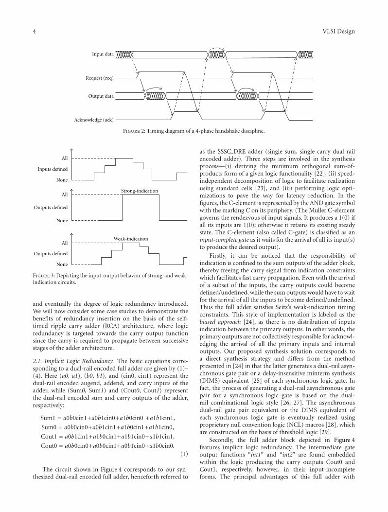
Seitz classified a self-timed logic circuit into two robustcategories on the basis of its indicating (acknowledging)genre as strongly indicating and weakly indicating [20]. It wasalso shown therein that a legal interconnection of strongly orweakly indicating logic circuits gives rise to a larger strong orweak-indication logic circuit.
(i) Strong Indication. In this case, the self-timed circuitwaits for all of its inputs (valid/spacer) to arrivebefore it starts to produce all the outputs (valid/spacer). The sequencing constraints are given below:
(a) all the inputs become defined (valid)/undefined(spacer) before any output becomes defined/undefined; that is, any or all of the output(s)become defined/undefined only after all theinputs have become defined/undefined,

VLSI Design 3
Table 1: Data representation via dual-rail and 1-of-4 encoding formats.
Single-rail inputs Dual-rail encoded data 1-of-4 encoded data
A B (A1 A0) (B1 B0) E0 E1 E2 E3
0 0 (0 1) (0 1) 0 0 0 1
0 1 (0 1) (1 0) 0 0 1 0
1 0 (1 0) (0 1) 0 1 0 0
1 1 (1 0) (1 0) 1 0 0 0
Ackout
Dual-rail data busSenderReceiver
Ackin
d00
d01
dn−10
dn−11
...
Figure 1: Delay-insensitive dual-rail data encoding and 4-phase handshaking.
(b) all the outputs become defined/undefined be-fore any input becomes undefined/defined.
(ii) Weak Indication. According to this, the self-timedcircuit is allowed to produce any of the outputs(valid/spacer) even with a subset of the inputs (valid/spacer). However, Seitz’s weak timing specificationsrequire that at least one output (valid/spacer) shouldnot have been produced until after all the inputs(valid/spacer) have arrived. The sequencing con-straints in this case are as follows.
(a) Some inputs become defined (undefined) be-fore some outputs become defined (undefined);that is, some outputs could become defined(undefined) only after at least some inputs havebecome defined (undefined).
(b) All the inputs become defined (undefined) be-fore all the outputs become defined (unde-fined); that is, all the outputs could become de-fined (undefined) only after all the inputs havebecome defined (undefined).
(c) All the outputs become defined (undefined)before any input becomes undefined (defined).
The signaling scheme for strong- and weak-indicationtiming regimes in terms of the input-output characteristicsis illustrated graphically in Figure 3, which summarizesthe sequencing constraints mentioned above. In generalfor iterative circuits, weakly indicating implementations arepreferable compared to strongly indicating versions since theformer’s computation time is data dependent for valid dataand may exhibit constant latency for spacer data, while thelatter is always bound by worst-case latency for both validdata and spacers [21].
2. Redundant Logic Insertion
This section deals with an efficient method of reducingthe critical path delay of self-timed adders by means of anovel concept called redundant logic insertion. In general,the concept can be extended to effect latency reduction inany iterative logic circuit that comprises a cascade of basicbuilding blocks. Redundancy insertion, in general, impliesinclusion of extra redundant logic into a non redundantimplementation without modifying the original functionthat synthesizes the desired functionality to enable speedingup the propagation of certain signals, which are required todrive the subsequent stages of a circuit cascade.
Logic redundancy can be incorporated into a self-timedcircuit implementation by careful duplication of similarlogic, and this can lead to multiple acknowledgements, whichmight be useful in simplifying the timing assumptions.Additionally, this procedure could facilitate faster reset oflogic during the return-to-zero phase with a constant latency.Logic redundancy achieved through input-incomplete gatesbasically introduces weak-indication property into the circuitas it relaxes the indication constraints of those outputsthat are considered as candidates for optimization. (Input-incomplete gates need not have to wait for the arrival ofall their inputs to produce the required output under allscenarios; examples include AND gates and OR gates. Ifany one of its inputs is assigned a 0(1), the output of theAND gate (OR gate) becomes a 0(1)). It can either beimplicit or explicit in the circuit. The minor drawbacks ofthis approach are insignificant increases in area and powerparameters. Since logic duplication is involved, switchingactivity would increase due to multiple acknowledgements,consequently pushing up the dynamic power and resultingin increased average power dissipation. However, the areaand power overheads may be marginal depending upon thefunctionality and its initial nonredundant implementation,
4 VLSI Design
Input data
Request (req)
Output data
Acknowledge (ack)
Figure 2: Timing diagram of a 4-phase handshake discipline.
Inputs defined
None
All
All
None
Outputs defined
All
None
Outputs defined
Strong-indication
Weak-indication
Figure 3: Depicting the input-output behavior of strong-and weak-indication circuits.
and eventually the degree of logic redundancy introduced.We will now consider some case studies to demonstrate thebenefits of redundancy insertion on the basis of the self-timed ripple carry adder (RCA) architecture, where logicredundancy is targeted towards the carry output functionsince the carry is required to propagate between successivestages of the adder architecture.
2.1. Implicit Logic Redundancy. The basic equations corre-sponding to a dual-rail encoded full adder are given by (1)–(4). Here (a0, a1), (b0, b1), and (cin0, cin1) represent thedual-rail encoded augend, addend, and carry inputs of theadder, while (Sum0, Sum1) and (Cout0, Cout1) representthe dual-rail encoded sum and carry outputs of the adder,respectively:
Sum1 = a0b0cin1+a0b1cin0+a1b0cin0 +a1b1cin1,
Sum0 = a0b0cin0+a0b1cin1+a1b0cin1+a1b1cin0,
Cout1 = a0b1cin1+a1b0cin1+a1b1cin0+a1b1cin1,
Cout0 = a0b0cin0+a0b0cin1+a0b1cin0+a1b0cin0.(1)
The circuit shown in Figure 4 corresponds to our syn-thesized dual-rail encoded full adder, henceforth referred to
as the SSSC DRE adder (single sum, single carry dual-railencoded adder). Three steps are involved in the synthesisprocess—(i) deriving the minimum orthogonal sum-of-products form of a given logic functionality [22], (ii) speed-independent decomposition of logic to facilitate realizationusing standard cells [23], and (iii) performing logic opti-mizations to pave the way for latency reduction. In thefigures, the C-element is represented by the AND gate symbolwith the marking C on its periphery. (The Muller C-elementgoverns the rendezvous of input signals. It produces a 1(0) ifall its inputs are 1(0); otherwise it retains its existing steadystate. The C-element (also called C-gate) is classified as aninput-complete gate as it waits for the arrival of all its input(s)to produce the desired output).
Firstly, it can be noticed that the responsibility ofindication is confined to the sum outputs of the adder block,thereby freeing the carry signal from indication constraintswhich facilitates fast carry propagation. Even with the arrivalof a subset of the inputs, the carry outputs could becomedefined/undefined, while the sum outputs would have to waitfor the arrival of all the inputs to become defined/undefined.Thus the full adder satisfies Seitz’s weak-indication timingconstraints. This style of implementation is labeled as thebiased approach [24], as there is no distribution of inputsindication between the primary outputs. In other words, theprimary outputs are not collectively responsible for acknowl-edging the arrival of all the primary inputs and internaloutputs. Our proposed synthesis solution corresponds toa direct synthesis strategy and differs from the methodpresented in [24] in that the latter generates a dual-rail asyn-chronous gate pair or a delay-insensitive minterm synthesis(DIMS) equivalent [25] of each synchronous logic gate. Infact, the process of generating a dual-rail asynchronous gatepair for a synchronous logic gate is based on the dual-rail combinational logic style [26, 27]. The asynchronousdual-rail gate pair equivalent or the DIMS equivalent ofeach synchronous logic gate is eventually realized usingproprietary null convention logic (NCL) macros [28], whichare constructed on the basis of threshold logic [29].
Secondly, the full adder block depicted in Figure 4features implicit logic redundancy. The intermediate gateoutput functions “int1” and “int2” are found embeddedwithin the logic producing the carry outputs Cout0 andCout1, respectively, however, in their input-incompleteforms. The principal advantages of this full adder with

VLSI Design 5
cin0
cin1
cin1
cin1
cin1
cin0
cin0
cin0
Sum1Sum0
Cout1Cout0
int2
int1
C
C
C
CC
C
C
C
a0
a0
b1
b1
a1
b1
b1
a1
a1
a1
b0
a0
a0
b0
b0
b0
Figure 4: Proposed weak-indication full adder design (SSSC DRE adder).
Overflowcarry
Dual-rail encodedself-timed full adder
Dual-rail encodedself-timed full adder
a(n− 1)1a(n− 1)0
b(n− 1)1b(n− 1)0
Sum(n− 1)1 Sum(n− 1)0 Sum01 Sum00
Carryin1
Carryin0
Carry(n− 2)1
Carry(n− 2)0
Carry(0)1
Carry(0)0
a01a00
b01b00
· · ·
Figure 5: n-bit dual-rail encoded self-timed carry-ripple adder structure.
respect to the n-bit self-timed RCA architecture shown inFigure 5 are (i) fast carry output production and propagationwhen carry-generate (a1 = b1 = 1) and carry-kill (a0 =b0 = 1) conditions occur and (ii) reset of the entire addercircuitry with an approximate propagation delay of onlytwo full adders during the return-to-zero phase regardlessof the adder size. The latter advantage results from thefact that the intermediate dual-rail output carries of all thefull adder modules connected in a cascade could be resetin parallel as the dual-rail encoded augend and addendinputs of every adder stage are reset. Subsequently, the dual-rail sum outputs of all the adder stages would be reset astheir input carries assume a spacer state. This leads to aconstant latency operation for application of spacer data,while data-dependent latency would manifest when validdata is applied. Indeed, this attribute becomes inherentin all the redundancy incorporated self-timed adders. Theworst-case latency results when the carry-propagate mode isactivated with respect to all the individual full adder stages;this happens for the case when a1 = b0 = 1 or a0 = b1 = 1.
The SSSC DRE adder has some similar properties as that ofMartin’s full adder [30], which is nevertheless a stand-alonefull-custom transistor level realization.
2.2. Explicit Logic Redundancy. We now consider a varietyof scenarios where logic redundancy is explicit in a circuitdesign. To this end, we analyze some adder circuits whichemploy a uniform DI data encoding protocol (dual-railencoding) for both primary inputs and outputs, or a combi-nation of DI codes (dual-rail and 1-of-4 codes) for primaryinputs, but a single DI code (dual-rail code) for the primaryoutputs.
2.2.1. Single-Bit Adder Based on Hybrid Input Encoding. Theterm “hybrid input encoding” specifies a mix of at leasttwo different DI data encoding schemes as adopted for theprimary inputs. Considering the single-bit full adder block,the augend and addend input bits can be encoded using a1-of-4 code, while the carry input, sum and carry outputs

6 VLSI Design
Overflowcarry Hybrid input encoded
self-timed full adderHybrid input encodedself-timed full adder
Sum(n− 1)1 Sum(n− 1)0 Sum01 Sum00
Carryin1
Carryin0
Carry(n− 2)1
Carry(n− 2)0
Carry(0)1
Carry(0)0
· · ·
i(3)i(2)
i(1)i(0)
i(4n− 1)i(4n− 2)
i(4n− 3)i(4n− 4)
Figure 6: n-bit hybrid input encoded self-timed RCA configuration.
i3
i3
i0
i0
i2i1
cin1
cin1
cin0
cin0
Sum1Sum0
Cout1
Cout0
C
C
C
C
Figure 7: Hybrid input encoded full adder block (SSSC HIE NRLadder).
can adopt the dual-rail code; that is, hybrid encoding ofprimary inputs and uniform encoding of primary outputsare resorted to. The structure of the n-bit hybrid inputencoded self-timed RCA is depicted by Figure 6, which issimilar to the topology shown in Figure 5 with the exceptionthat the augend and addend single-rail inputs are nowencoded using the 1-of-4 code.
The general expressions governing a full adder blockutilizing hybrid input encoding for inputs and dual-railencoding for outputs are given below. In the equations thatfollow, (i0, i1, i2, i3) represents the 1-of-4 encoded equivalentof the single-rail adder inputs (a, b), with a single-rail to 1-of-4 data representation scheme adopted as shown in Table 1:
Sum1 = i3cin1 + i2cin0 + i1cin0 + i0cin1,
Sum0 = i3cin0 + i2cin1 + i1cin1 + i0cin0,
Cout1 = i2cin1 + i1cin1 + i0cin0 + i0cin1,
Cout0 = i3cin0 + i3cin1 + i2cin0 + i1cin0.
(2)
The full adder block that synthesizes equation (2)inclusive of carry output logic optimization is portrayed byFigure 7. Henceforth, this adder module shall be identifiedas the SSSC HIE NRL adder (single sum, single carry hybridinput encoded nonredundant logic adder). As the nameimplies, all the gates that constitute this adder are irredun-dant. It can be observed from Figure 7 that the sum outputsare entrusted with the responsibility of inputs indication,while the carry outputs could evaluate to the correct state
cin1
cin1
cin1
cin0
cin0
cin0
C
CSum1Sum0
Cout1
Cout0i3
i3
i0
i0
i2i1
C1
C2
g1
g2
Figure 8: Hybrid input encoded full adder including redundancy(SSSC HIE RL adder).
whenever the carry-kill or carry-generate condition occurswithout having to wait for the carry input. Thus theSSSC HIE NRL adder corresponds to the weak-indicationtiming model.
The synthesized hybrid input encoded full adder blockthat incorporates logic redundancy is shown in Figure 8.
Here, gates C1 and C2 denote 2-input C-elements, whilegates g1 and g2 represent 2-input AND gates. It can be noticedin the figure that the functions realized by C1 and C2 areidentical to that implemented by g1 and g2, respectively,for the case of upgoing transitions. Hence, redundancy isexplicit in the present design, henceforth referred to as theSSSC HIE RL adder (single sum, single carry hybrid inputencoded redundant logic adder). With respect to this adderdesign, logic redundancy is found to be beneficial in twoways. During the spacer phase, all the sum outputs couldbe reset in a parallel fashion, as the dual-rail carry outputof the kth stage of a n-bit adder could be reset based on its1-of-4 encoded augend and addend inputs, and the dual-rail sum output of the (k + 1)th adder stage would dependonly on the dual-rail carry input of its preceding stage. Thereis also a benefit in terms of improving the computationspeed during the valid data phase. This would be obviousby comparing the designs portrayed by Figures 7 and 8; itcan be observed that the carry propagation delay is less incase of the SSSC HIE RL adder (AND2, OR2 gate delays) in

VLSI Design 7
a(n− 1)1 a(n− 1)0 a(n− 2)0a(n− 2)1
Overflowcarry
ST DSSC adder module(DSSC CCO or DSSC CCAO local)
ST DSSC adder module(DSSC CCO or DSSC CCAO local)
Carryout(n− 3)1
Carryout(n− 3)0
Carryout(1)1
Carryout(1)0
Sum(n− 1)1
Sum(n− 1)0
Sum(n− 2)1
Sum(n− 2)0
Sum(1)1Sum(1)0
Sum(0)1Sum(0)0
a(1)1 a(1)0 a(0)1 a(0)0b(1)1 b(1)0 b(0)1 b(0)0b(n− 1)1 b(n− 1)0 b(n− 2)1 b(n− 2)0
Carryin
· · ·
Figure 9: Dual-rail encoded n-bit RCA architecture comprising dual-bit adder blocks.
comparison with the SSSC HIE NRL adder (CE2, OR2 gatedelays).
2.2.2. Dual-Bit Adder Utilizing Homogeneous Data Encod-ing. We now analyze the effect of introducing redundantlogic in a self-timed dual-bit adder module that employshomogeneous data encoding for both its primary inputs andoutputs. The homogeneous encoding procedure refers to asimilar DI data encoding protocol as adopted for all theprimary inputs and outputs of a function block—here dual-rail data encoding. The dual-bit adder block consists of dual-rail encoded versions of five single-rail inputs, namely, a1,a0, b1, b0, and cin, and three single-rail outputs Cout, Sum1and Sum0, where (a1, a0) and (b1, b0) represent the addendand augend inputs and cin the carry input. The output Coutis the carry output or overflow bit of the addition process,and Sum1 and Sum0 signify the most significant and leastsignificant sum output bits, respectively.
The reduced orthogonal sum-of-products forms corre-sponding to the encoded outputs of the dual-bit adder aregiven below, expressed in terms of their encoded inputs. In anorthogonal sum-of-products form, the logical conjunction ofany pair of product terms yields a null:
Cout1 = a10a00b11b01cin1+ a11a00b10b01cin1
+ a10a01b11b00cin1 + a11a01b10b00cin1
+ a10a01b11b01 + a11a01b10b01 + a11b11,
Cout0 = a11a01b10b00cin0 + a10a01b11b00cin0
+ a11a00b10b01cin0 + a10a00b11b01cin0
+ a11a00b10b00 + a10a00b11b00 + a10b10,
Sum11 = a11a01b10b00cin0 + a10a01b11b00cin0
+ a11a00b10b01cin0 + a10a00b11b01cin0
+ a11a00b11b01cin1 + a11a01b11b00cin1
+ a10a00b10b01cin1 + a10a01b10b00cin1
+ a10a01b10b01 + a11a00b10b00
+ a10a00b11b00 + a11a01b11b01,
Sum10 = a11a01b10b00cin1 + a10a01b11b00cin1
+ a11a00b10b01cin1 + a10a00b11b01cin1
+ a10a01b10b00cin0 + a10a00b10b01cin0
+ a11a01b11b00cin0 + a11a00b11b01cin0
+ a11a00b11b00 + a11a01b10b01
+ a10a01b11b01 + a10a00b10b00,
Sum01 = a01b00cin0 + a00b01cin0
+ a00b00cin1 + a01b01cin1,
Sum00 = a01b01cin0 + a01b00cin1
+ a00b01cin1 + a00b00cin0.
(3)
The architecture of the n-bit self-timed carry-rippleadder structure that features dual-bit adder modules isshown in Figure 9. The synthesized dual-bit adder moduleis portrayed by Figure 10. It shall be referred to as theDSSC DRE adder module (dual sum, single carry dual-railencoded adder) in the subsequent discussions. Figure 10depicts the redundant AND gates (shaded gates) insertedinto the DSSC DRE adder block. The nonredundant adderblock would not feature the AND gates rg1 and rg2, andso one of the inputs for the OR2 gates producing Cout1and Cout0 would be the outputs of C-elements (C1 andC2), which are the nets labeled as gn2 and gn3, respectively.In fact, gn2 and gn3 would be isochronic forks in thenonredundant version. Isochronic forks are the weakest com-promise to delay insensitivity [31], leading to quasidelay-insensitive (QDI) circuit implementations. According to theisochronicity assumption, if a transition on a wire fork isacknowledged, then the transition on the other wire forksis also said to be acknowledged. It was shown in [32] thatQDI circuits which include isochronic fork assumptions canbe realized in even nanometer scale dimensions. Indeed, QDIcircuits are the practically implementable DI circuits, andthey constitute the robust class of self-timed circuits. In theredundant dual-bit adder shown in Figure 10, the OR2 gatesproducing Cout1 and Cout0 have gn1 and gn4 feeding as

8 VLSI Design
a10
a10
a10
a10
a10
a10
a10
a00
a01
a01
a01
a01
a01
a01
a01
a01
b11
b11
b11
b11
b11
b11
b11
b01
b00
b00
b00
b00
b01
b01
b01
b01
b01
b01
b01
a11
a11
a11
a11
a11
a11
a11b11a11
a00
a00
a00
b00
b00
a00
a00
b10
b10
b10
a10b10
b10
b10
b10
b10
b11a11
a10b10
b00
b01
b01
b00
b00
b00
a00
a00
a00
a01
a01
a00
C
C
C
C
C
C
C
C
C
C
C
C
C
C
C
C
C
C
C
C
C
C
C
C
C1
C2
Cout1
Cout0
Sum11
Sum10
Sum01Sum00
cin1
cin1
cin0
cin0
isf
cin0
cin0
cin1
cin1
cin1 gn1
rg2
rg1
gn2
gn3
gn4
cin0
Figure 10: Redundant logic insertion in a homogeneously encoded dual-bit adder.
inputs, respectively. For the case of low-to-high transitions,the AND gates rg1 and rg2 are functionally equivalent to C-elements C1 and C2.
The gate output node labeled “isf ” signifies an isochronicfork junction. Referring to Figure 10, it can be observed
that an upgoing transition on the fork isf (isf ↑) wouldbe followed by either gn2↑ or gn3↑ in case of the nonre-dundant DSSC DRE adder block and by (gn1↑, gn2↑) or(gn3↑, gn4↑) in case of the DSSC DRE adder module thatincorporates logic redundancy; this explains the possible

VLSI Design 9
Sum3
Sum2
Sum1
Sum0
Cout1
Cout0
C
C
C
C
C
C
C
C
C
C
C
C
C
C
C
C
C
C
C
C
C
C
C1
C2
cin0
cin1
cin0
cin0
cin0
cin0
cin1
cin1
cin1
cin1
isf
rg2
rg1gn1
gn2
gn3
gn4
a0b0
b1
b0
b0
b3
b0
a0
a0
a0
b1
b1
b1
b2
b2
b2
b3
b3
b2
b3
a2
a3
a3
a3
a3
a2
a2
a2
a1
a1
a1
a1
Figure 11: Weakly indicating heterogeneously encoded dual-bit adder module.
multiple acknowledgements. It can be observed that there isa possibility for fast or eager reset during the return-to-zerophase as a result of introducing logic redundancy into theadder. During the spacer phase, all the sum outputs could bereset in a parallel fashion, as the carry output of the previousdual-bit adder stage could be reset even by its correspondingaugend and addend inputs without having to wait for aninput carry from the preceding stage. The advantage oflatency reduction gained by introduction of redundant logic
is due to the lower data path delay encountered, as thecritical path in every dual-bit adder stage contains input-incomplete gates instead of a mix of input-complete andinput-incomplete gates as in the original nonredundantversion.
2.2.3. Dual-Bit Adder Incorporating Heterogeneous Data En-coding. The heterogeneous encoding procedure implies acombination of at least two different DI codes (say, dual-rail

10 VLSI Design
Heterogeneously encoded dual-bit ST adder
Heterogeneously encoded dual-bit ST adder
a(2n− 1) a(2n− 3) b(2n− 1) b(2n− 3)
a(2n− 2) a(2n− 4) b(2n− 2) b(2n− 4)
Sum(2n− 1) Sum(2n− 3)
Sum(2n− 2) Sum(2n− 4)
a(3) a(1) b(3) b(1)
a(2) a(0) b(2) b(0)
Carry(n− 2)1
Carry(n− 2)0
· · ·
Sum(3)
Sum(2)
Sum(1)
Sum(0)
Carryin(1)
Carryin(0)
Carry(1)1
Carry(1)0
Overflowcarry
Figure 12: Heterogeneously encoded dual-bit adder based n-bit self-timed RCA.
Next stage
register
Completion detection logic
Current stage register
Ackout
AckoutAckin
Ackin
Self-timed logic blockEncoder
Subset of dual-rail inputs
Remainder of dual-rail inputs
Decoder
Completion detection logic
(a)
a0
b0
a1
b1
i0
i1
i2
i3
C
C
C
C
(b)
a0
b0
a1
b1
i0
i1
i2
i3
(c)
Figure 13: (a) Self-timed system handling heterogeneously encoded inputs and outputs, (b) dual-rail to 1-of-4 encoder, (c) 1-of-4 to dual-rail decoder.
and 1-of-4 codes), used to encode the primary inputs andoutputs of a self-timed logic circuit. A dual-bit adder blockbased on heterogeneous DI data encoding can represent theaugend, addend inputs, and sum outputs by a 1-of-4 code,while the input and output carry signals can be representedusing the dual-rail code. Adopting such an encoding scheme,the minimized expressions for the function block outputs aregiven below. It is to be noted that the 1-of-4 code assignments
for the augend, addend inputs, and the sum outputs are thereverse of the assignments given in Table 1:
Cout1 = a0b3cin1 + a1b2cin1 + a2b1cin1
+ a3b0cin1 + a1b3 + a2b2 + a3b1
+ a2b3 + a3b2 + a3b3,
(4)

VLSI Design 11
Cout0 = a0b3cin0 + a1b2cin0 + a2b1cin0
+ a3b0cin0 + a0b0 + a0b1
+ a0b2 + a1b0 + a1b1 + a2b0,
(5)
Sum3 = a0b3cin0 + a1b2cin0 + a2b1cin0
+ a3b0cin0 + a0b2cin1 + a1b1cin1
+ a2b0cin1 + a3b3cin1,
(6)
Sum2 = a0b2cin0 + a1b1cin0 + a2b0cin0
+ a3b3cin0 + a0b1cin1 + a1b0cin1
+ a2b3cin1 + a3b2cin1,
(7)
Sum1 = a0b1cin0 + a1b0cin0 + a2b3cin0
+ a3b2cin0 + a0b0cin1 + a1b3cin1
+ a2b2cin1 + a3b1cin1,
(8)
Sum0 = a0b0cin0 + a1b3cin0 + a2b2cin0
+ a3b1cin0 + a0b3cin1 + a1b2cin1
+ a2b1cin1 + a3b0cin1.
(9)
The dual-bit adder module that synthesizes (4)–(9)is shown in Figure 11. Henceforth, this adder shall bereferred to as the DSSC HE adder (dual sum, single carryheterogeneously encoded adder). The DSSC HE adder blocksatisfies the weak-indication timing constraints. The 1-of-4encoded sum outputs assume responsibility for indicatingthe arrival of all the adder inputs, while the dual-rail encodedcarry output can be relaxed with respect to ensuring inputcompleteness. Logic redundancy, as introduced into theDSSC HE adder module, is shown in the figure with theinput-incomplete AND gates (shaded gates) marked as rg1and rg2. Similar notations have been used as that of Figure 10so that the discussions of the previous section would holdwell for this scenario too. As in the earlier case, the sumoutput(s) of the (i+1)th dual-bit adder stage could be resetbased on the carry input from the ith dual-bit adder stage,and there does not arise any need for resetting of the entirecarry chain during the return-to-zero phase.
The n-bit self-timed carry-ripple adder architecturethat encompasses heterogeneously encoded dual-bit addermodules is shown in Figure 12. The self-timed systemconfiguration that supports the RCA topology is depictedin Figure 13. A subset of the dual-rail inputs (augends andaddends) is 1-of-4 encoded before being fed to the functionblock for data processing, while the remaining inputs (dual-rail encoded input carry) are fed as such. The non-dual-rail outputs produced by the logic block (sum outputs)are decoded before being passed onto the next stage, whilethe dual-rail outputs (output carry) are driven to the nextstage. The encoding and decoding costs equate to 28 and 12transistors per bit, respectively.
3. Simulation Mechanism and Results
To demonstrate the usefulness of the proposed conceptof logic redundancy insertion, simulations have been per-formed by considering a 32-bit self-timed RCA architecture.In this context, a subset of well-known self-timed designmethods [25, 33, 34] is considered in this work. Various32-bit self-timed RCAs were built by considering differentadder building blocks—32 single-bit adder blocks or 16dual-bit adder modules. Before discussing the simulationresults, the mechanism of estimating the design metrics iselucidated. The delay parameter refers to the maximumpropagation delay (critical path delay) encountered in thedata path, which is a sum of the latencies of the inputregister and that of the combinatorial adder logic. Thedelay metric was estimated using PrimeTime. To avoid thenotion of a clock source, a virtual clock was used as aremote reference to constrain the input and output ports ofthe design. The area and power metrics correspond to theinput registers, completion detection logic, and the 32-bitcombinatorial adder. The delay and power metrics considerestimated parasitics in addition to the parameters associatedwith actual components (gates). The area metric gives acombined account of the area of all the logic cells. Thetotal/average power dissipation is the sum of dynamic andstatic power components, where dynamic power is in turncomposed of switching and internal power consumptionvalues. NC-Sim has been used for functional simulationand also to obtain the switching activity files correspondingto gate-level simulations of Verilog descriptions of various32-bit self-timed adders. Input data were supplied to theadders at a time interval of 15 ns through a random testbench which models the environment. The switching activityfiles obtained were subsequently used for power estimationusing PrimeTime PX. The simulations targeted a PVT cornerof the 130 nm bulk CMOS standard cell library whoserecommended supply voltage is 1.32 V and the ambientjunction temperature is −40◦C. All the circuit inputs possessthe driving strength of the minimum-sized inverter of thecell library, while the outputs are associated with a fanout-of-4 drive strength. Appropriate buffering for the inputacknowledgement signal was provided where necessary toeliminate timing violations. Since identical registers and asimilar completion detection circuit were used for all the 32-bit adders, the area and power metrics can be correlated withthat of the function block, thus paving the way for a straight-forward comparison between adders synthesized on thebasis of different self-timed design methods. Strong/weak-indication adders corresponding to various self-timed designmethods were constructed manually and were subsequentlyoptimized for minimum latency by taking into account thephysical constraints of the target cell library. (A 130 nmCMOS standard cell library was used. The maximum fan-in of AND gate and OR gate in this library is 4 and 3,respectively. The granularity of the C-element ranges from2 to 4 inputs, and the gate level C-element models are givenin [35]). The delay, area, and power metrics correspondingto the simulations of various nonredundant 32-bit self-timedRCAs are given in Table 2.

12 VLSI Design
Table 2: Delay, area, and power of various nonredundant 32-bit self-timed RCAs.
Adder realization style Delay (ns) Area (µm2) Power (µW)
SSSC HIE NRL (weak) 8.0 6633 (78) 619.1
DIMS DSSC DRE (weak)∗ [25] 12.8 21833 (1202) 1025.9
Toms DSSC DRE (strong) [33] 9.4 10793 (512) 693.1
Toms DSSC HE (strong) [33] 9.0 12121 (479) 695.9
Folco et al. DSSC DRE (weak) [34] 5.9 9417 (426) 740.4
DSSC DRE (weak) 5.9 14921 (770) 871.9
DSSC HE (weak) 5.8 10889 (402) 688.4∗The dual sum, single carry (DSSC) adder realization based on the DIMS method required careful speed-independent logic decomposition to decompose thehigh fan-in C-gates.
Table 3: Delay, area, and power metrics of various redundant 32-bit self-timed RCAs.
Adder realization style Delay (ns) Area (µm2) Power (µW)
SSSC HIE RL (weak) 5.9 6953 (88) 630.2
DIMS DSSC DRE (weak) [25] 10.5 22473 (1242) 1034.6
Folco et al. DSSC DRE (weak) [34] 4.7 9577 (436) 743.8
DSSC DRE (weak) 4.6 15081 (780) 875.3
DSSC HE (weak) 4.6 11049 (412) 691.9
The nature of indication of the different adders ismentioned within brackets in the 1st column of the Table.The values specified within brackets in the 3rd columnof the table signify the area of the respective individualsingle-bit/dual-bit self-timed adder block. The delay, areaand power parameters of the different redundant logicincorporated 32-bit self-timed RCAs are given in Table 3.Introduction of logic redundancy into the dual-bit addermodule synthesized on the basis of Toms and Edwards,approach [33] was not considered, since it would changethe indication property of the original synthesis solution.Therefore, redundant versions of other adders were aloneconsidered for comparison in Table 3. By comparing theresults given in Tables 2 and 3, it is found that logicredundancy insertion has enabled a mean delay reductionof 21.1%, with associated area and power penalties to thetune of 2.3% and 0.8%, respectively. On average, the increasein size of an individual self-timed single-bit/dual-bit addermodule is found to be 2.8% after incorporating redundantlogic.
With reference to the DSSC HE adder module shown inFigure 11, a further peephole optimization was carried out bymerging the gate rg1 and the OR gate producing Cout1 andrg2 and the OR gate producing Cout0 and replacing thesecombinations using complex gates (AO12 cells). Simulationswere repeated for this case study, and the delay, area, andpower values corresponding to the 32-bit RCA, comprisingoptimized redundant DSSC HE adder blocks, are foundto be 4 ns, 10953 µm2, and 696.8 µW respectively. Theoptimized redundant DSSC HE adder block occupies lessarea than the nonoptimized redundant DSSC HE adderblock by 1.5%. Hence, the 32-bit self-timed RCA comprisinga cascade of optimized redundant DSSC HE adder blocksexhibits reduced delay in comparison with the nonredundantDSSC HE adder module based 32-bit self-timed RCA by
31%. However, in terms of area and average power, thelatter features reduced figures to the tune of 0.6% and 1.2%,respectively, compared to the former.
4. Conclusions
A new concept of redundant logic insertion was described inthis paper that can be used to minimize the data path delay ofself-timed arithmetic circuits. It was shown that introductionof logic redundancy is feasible with respect to many self-timed design methods, especially for synthesizing iterativelogic specifications. The advantages of logic redundancyinsertion have been propounded on the basis of a 32-bitself-timed carry-ripple addition. It has been inferred fromthe simulation results that significant reduction in latencycould be achieved at the expense of only marginal increasesin area and power metrics. It was also discussed how logicredundancy paves the way for constant latency operation bypermitting fast reset when applying spacer data, while actualcase latency is encountered for addition of valid data.
Acknowledgments
This research was supported in part by the Engineeringand Physical Sciences Research Council, UK, under GrantEP/D052238/1. The first author was additionally supportedby a bursary from the School of Computer Science of theUniversity of Manchester.
References
[1] “Semiconductor Industry Association’s International Tech-nology Roadmap for Semiconductors,” Design Report, 2009,http://www.itrs.net/.

VLSI Design 13
[2] A. J. Martin, S. M. Burns, T. K. Lee, D. Borkovic, and P. J.Hazewindus, “The first asynchronous microprocessor: the testresults,” ACM SIGARCH Computer Architecture News, vol. 17,no. 4, pp. 95–98, 1989.
[3] K. J. Kulikowski, V. Venkataraman, Z. Wang, A. Taubin, andM. Karpovsky, “Asynchronous balanced gates tolerant to inter-connect variability,” in Proceedings of the IEEE InternationalSymposium on Circuits and Systems (ISCAS ’08), pp. 3190–3193, May 2008.
[4] I. J. Chang, S. P. Park, and K. Roy, “Exploring asynchronousdesign techniques for process-tolerant and energy-efficientsubthreshold operation,” IEEE Journal of Solid-State Circuits,vol. 45, no. 2, pp. 401–410, 2010.
[5] M. Zamani and M. B. Tahoori, “A transient error tolerantself-timed asynchronous architecture,” in Proceedings of the15th IEEE European Test Symposium (ETS’10), pp. 88–93, May2010.
[6] J. Hamon and L. Fesquet, “Robust and programmable self-timed ring oscillators,” in Proceedings of the IEEE 9th Interna-tional New Circuits and Systems Conference (NEWCAS ’11), pp.249–252, 2011.
[7] T. Chelcea, G. Venkataramani, and S. C. Goldstein, “Area opti-mizations for dual-rail circuits using relative-timing analysis,”in Proceedings of the 13th IEEE International Symposium onAsynchronous Circuits and Systems, pp. 1–12, 2007.
[8] G. F. Bouesse, G. Sicard, A. Baixas, and M. Renaudin,“Quasi delay insensitive asynchronous circuits for low EMI,”in Proceedings of the 4th International Workshop on Electro-Magnetic Compatibility of Integrated Circuits, pp. 27–31, 2004.
[9] W. A. Lien, P. Day, C. Farnsworth et al., “Noise in self-timedand synchronous implementations of a DSP,” in Proceedings ofthe IEEE Radio and Wireless Conference, pp. 75–78, 1998.
[10] L. S. Nielsen, C. Niessen, J. Sparso, and K. van Berkel, “Low-power operation using self-timed circuits and adaptive scalingof the supply voltage,” IEEE Transactions on Very Large ScaleIntegration (VLSI) Systems, vol. 2, no. 4, pp. 391–397, 1994.
[11] O. C. Akgun, J. Rodrigues, and J. Sparsø, “Minimum-energysub-threshold self-timed circuits: design methodology anda case study,” in Proceedings of the 16th IEEE InternationalSymposium on Asynchronous Circuits and Systems (ASYNC’10), pp. 41–51, May 2010.
[12] C. H. Van Kees Berkel, M. B. Josephs, and S. M. Nowick,“Scanning the technology applications of asynchronous cir-cuits,” Proceedings of the IEEE, vol. 87, no. 2, pp. 223–233,1999.
[13] I. David, R. Ginosar, and M. Yoeli, “Self-timed is self-checking,” Journal of Electronic Testing, vol. 6, no. 2, pp. 219–228, 1995.
[14] S. J. Piestrak and T. Nanya, “Towards totally self-checkingdelay-insensitive systems,” in Proceedings of the 25th Interna-tional Symposium on Fault-Tolerant Computing, pp. 228–237,June 1995.
[15] T. Verhoeff, “Delay-insensitive codes—an overview,” Dis-tributed Computing, vol. 3, no. 1, pp. 1–8, 1988.
[16] B. Bose, “On unordered codes,” IEEE Transactions on Comput-ers, vol. 40, no. 2, pp. 125–131, 1991.
[17] D. W. Lloyd and J. D. Garside, “A practical comparison of asyn-chronous design styles,” in Proceedings of the 7th InternationalSymposium on Asynchronous Circuits and Systems, (ASYNC’01), pp. 36–45, March 2010.
[18] W. J. Bainbridge, W. B. Toms, D. A. Edwards, and S. B. Furber,“Delay-insensitive, point-to-point interconnect using M-of-Ncodes,” in Proceedings of the 9th IEEE International Symposium
on Asynchronous Circuits and Systems, (ASYNC ’03), pp. 132–140, May 2003.
[19] V. Akella, N. H. Vaidya, and G. R. Redinbo, “Limitations ofVLSI implementation of delay-sensitive codes,” in Proceedingsof the 1996 26th International Symposium on Fault-TolerantComputing, pp. 208–217, June 1996.
[20] C. L. Seitz, “System timing,” in Introduction to VLSI Systems,C. Mead and L. Conway, Eds., pp. 218–262, Addison-Wesley,Reading, Mass, USA, 1980.
[21] J. Sparso and S. B. Furber, Eds., Principles of AsynchronousCircuit Design: A Systems Perspective, Kluwer Academic Pub-lishers, 2001.
[22] P. Balasubramanian and D.A. Edwards, “Self-timed realizationof combinational logic,” in Proceedings of the 19th InternationalWorkshop on Logic and Synthesis, pp. 55–62, 2010.
[23] P. Balasubramanian and D. A. Edwards, “A new design tech-nique for weakly indicating function blocks,” in Proceedings ofthe 11th IEEE Workshop on Design and Diagnostics of ElectronicCircuits and Systems (DDECS ’08), pp. 116–121, April 2008.
[24] C. Jeong and S. M. Nowick, “Block-level relaxation for timing-robust asynchronous circuits based on eager evaluation,” inProceedings of the 14th IEEE International Symposium onAsynchronous Circuits and Systems (ASYNC ’08), pp. 95–104,April 2008.
[25] J. Sparsø and J. Staunstrup, “Delay-insensitive multi-ringstructures,” Integration, The VLSI Journal, vol. 15, no. 3, pp.313–340, 1993.
[26] “Aperiodic circuits,” in Self-Timed Control of ConcurrentProcesses: The Design of Aperiodic Logical Circuits in Computersand Discrete Systems, V. I. Varshavsky, Ed., chapter 4, pp. 77–85, Kluwer Academic Publishers, 1990.
[27] C. D. Nielsen, “Evaluation of function block designs,” Tech.Rep. ID-TR: 1994-135, Department of Computer Science,Technical University of Denmark, 1994.
[28] K. M. Fant and G. E. Sobelman, “Null convention thresholdgate,” US Patent 5664211, 1997.
[29] P. M. LewisII and C. L. Coates, Threshold Logic, Wiley, NewYork, NY, USA, 1967.
[30] A. J. Martin, “Asynchronous datapaths and the design of anasynchronous adder,” Formal Methods in System Design, vol. 1,no. 1, pp. 117–137, 1992.
[31] A.J. Martin, “The limitation to delay-insensitivity in asyn-chronous circuits,” in Proceedings of the 6th MIT Conferenceon Advanced Research in VLSI, pp. 263–278, 1990.
[32] A. J. Martin and P. Prakash, “Asynchronous nano-electronics:preliminary investigation,” in Proceedings of the 14th IEEEInternational Symposium on Asynchronous Circuits and Systems(ASYNC ’08), pp. 58–68, gbr, April 2008.
[33] W. B. Toms and D. A. Edwards, “Efficient synthesis of speedindependent combinational logic circuits,” in Proceedings ofthe 10th Asia and South-Pacific Design Automation Conference,pp. 1022–1026, 2005.
[34] B. Folco, V. Bregier, L. Fesquet, and M. Renaudin, “Technologymapping for area optimized quasi delay insensitive circuits,” inProceedings of the IFIP International Conference on VLSI-SoC,pp. 146–151, 2005.
[35] P. Balasubramanian, Self-timed logic and the design of self-timed adders, Ph.D. thesis, The University of Manchester, 2010.

International Journal of
AerospaceEngineeringHindawi Publishing Corporationhttp://www.hindawi.com Volume 2010
RoboticsJournal of
Hindawi Publishing Corporationhttp://www.hindawi.com Volume 2014
Hindawi Publishing Corporationhttp://www.hindawi.com Volume 2014
Active and Passive Electronic Components
Control Scienceand Engineering
Journal of
Hindawi Publishing Corporationhttp://www.hindawi.com Volume 2014
International Journal of
RotatingMachinery
Hindawi Publishing Corporationhttp://www.hindawi.com Volume 2014
Hindawi Publishing Corporation http://www.hindawi.com
Journal ofEngineeringVolume 2014
Submit your manuscripts athttp://www.hindawi.com
VLSI Design
Hindawi Publishing Corporationhttp://www.hindawi.com Volume 2014
Hindawi Publishing Corporationhttp://www.hindawi.com Volume 2014
Shock and Vibration
Hindawi Publishing Corporationhttp://www.hindawi.com Volume 2014
Civil EngineeringAdvances in
Acoustics and VibrationAdvances in
Hindawi Publishing Corporationhttp://www.hindawi.com Volume 2014
Hindawi Publishing Corporationhttp://www.hindawi.com Volume 2014
Electrical and Computer Engineering
Journal of
Advances inOptoElectronics
Hindawi Publishing Corporation http://www.hindawi.com
Volume 2014
The Scientific World JournalHindawi Publishing Corporation http://www.hindawi.com Volume 2014
SensorsJournal of
Hindawi Publishing Corporationhttp://www.hindawi.com Volume 2014
Modelling & Simulation in EngineeringHindawi Publishing Corporation http://www.hindawi.com Volume 2014
Hindawi Publishing Corporationhttp://www.hindawi.com Volume 2014
Chemical EngineeringInternational Journal of Antennas and
Propagation
International Journal of
Hindawi Publishing Corporationhttp://www.hindawi.com Volume 2014
Hindawi Publishing Corporationhttp://www.hindawi.com Volume 2014
Navigation and Observation
International Journal of
Hindawi Publishing Corporationhttp://www.hindawi.com Volume 2014
DistributedSensor Networks
International Journal of


![Memory Chips with Adjustable Configurations*downloads.hindawi.com/journals/vlsi/1999/062801.pdf · [20]. Forinstance, the lookuptables ontheXilinx XC4000series ofFPGAscanbeusedto](https://img.pdfslide.us/doc/110x75/5f62cc48f8bed61af8350d0b/memory-chips-with-adjustable-configurations-20-forinstance-the-lookuptables.jpg)