Embed Size (px)
Citation preview

Brigham Young University Brigham Young University
BYU ScholarsArchive BYU ScholarsArchive
Theses and Dissertations
2007-02-27
Reducing Power in FPGA Designs Through Glitch Reduction Reducing Power in FPGA Designs Through Glitch Reduction
Nathaniel Hatley Rollins Brigham Young University - Provo
Follow this and additional works at: https://scholarsarchive.byu.edu/etd
Part of the Electrical and Computer Engineering Commons
BYU ScholarsArchive Citation BYU ScholarsArchive Citation Rollins, Nathaniel Hatley, "Reducing Power in FPGA Designs Through Glitch Reduction" (2007). Theses and Dissertations. 1105. https://scholarsarchive.byu.edu/etd/1105
This Thesis is brought to you for free and open access by BYU ScholarsArchive. It has been accepted for inclusion in Theses and Dissertations by an authorized administrator of BYU ScholarsArchive. For more information, please contact [email protected], [email protected].

REDUCING POWER IN FPGA DESIGNS THROUGH
GLITCH REDUCTION
by
Nathaniel H. Rollins
A thesis submitted to the faculty of
Brigham Young University
in partial fulfillment of the requirements for the degree of
Master of Science
Department of Electrical and Computer Engineering
Brigham Young University
April 2007


Copyright c© 2007 Nathaniel H. Rollins
All Rights Reserved


BRIGHAM YOUNG UNIVERSITY
GRADUATE COMMITTEE APPROVAL
of a thesis submitted by
Nathaniel H. Rollins
This thesis has been read by each member of the following graduate committee andby majority vote has been found to be satisfactory.
Date Michael J. Wirthlin, Chair
Date Brent E. Nelson
Date Doran K. Wilde


BRIGHAM YOUNG UNIVERSITY
As chair of the candidate’s graduate committee, I have read the thesis of NathanielH. Rollins in its final form and have found that (1) its format, citations, and bibli-ographical style are consistent and acceptable and fulfill university and departmentstyle requirements; (2) its illustrative materials including figures, tables, and chartsare in place; and (3) the final manuscript is satisfactory to the graduate committeeand is ready for submission to the university library.
Date Michael J. WirthlinChair, Graduate Committee
Accepted for the Department
Michael A. JensenChair
Accepted for the College
Alan R. ParkinsonDean, Ira A. Fulton College ofEngineering and Technology


ABSTRACT
REDUCING POWER IN FPGA DESIGNS THROUGH
GLITCH REDUCTION
Nathaniel H. Rollins
Department of Electrical and Computer Engineering
Master of Science
While FPGAs provide flexibility for performing high performance DSP func-
tions, they consume a significant amount of power. Often, a large portion of the
dynamic power is wasted on unproductive signal glitches. Reducing glitching reduces
dynamic energy consumption. In this study, retiming is used to reduce the unpro-
ductive energy wasted in signal glitches. Retiming can reduce energy by up to 92%.
Evaluating energy consumption is an important part of energy reduction. In
this work, an activity rate-based power estimation tool is introduced to provide FPGA
architecture independent energy estimations at the gate level. This tool can accu-
rately estimate power consumption to within 13% on average.
This activation rate-based tool and retiming are combined in a single algorithm
to reduce energy consumption of FPGA designs at the gate level. In this work,
an energy evaluation metric called energy area delay is used to weigh the energy
reduction and clock rate improvements gained from retiming against the area and
latency costs. For a set of benchmark designs, the algorithm that combines retiming
and the activation rate-based power estimator reduces power on average by 40% and
improves clock rate by 54% for an average 1.1× area cost and a 1.5× latency increase.


Table of Contents
List of Tables xv
List of Figures xix
1 Introduction 1
1.1 Thesis Contributions . . . . . . . . . . . . . . . . . . . . . . . . . . . 2
1.2 Thesis Overview . . . . . . . . . . . . . . . . . . . . . . . . . . . . . . 3
2 Power Consumption in FPGAs 5
2.1 Power in Digital Circuits . . . . . . . . . . . . . . . . . . . . . . . . . 5
2.1.1 Dynamic Power . . . . . . . . . . . . . . . . . . . . . . . . . . 6
2.1.2 Reducing Dynamic Power . . . . . . . . . . . . . . . . . . . . 8
2.1.3 Reducing Dynamic Power by Reducing Glitching . . . . . . . 8
2.2 FPGA Power . . . . . . . . . . . . . . . . . . . . . . . . . . . . . . . 9
2.3 FPGA Power Reduction Techniques . . . . . . . . . . . . . . . . . . . 11
2.3.1 Power Reduction at the FPGA Device Level . . . . . . . . . . 11
2.3.2 Power Reduction during Technology Mapping . . . . . . . . . 12
2.3.3 Power Reduction at the Gate Level . . . . . . . . . . . . . . . 13
3 FPGA Power Evaluation Techniques 15
3.1 Power Measurement . . . . . . . . . . . . . . . . . . . . . . . . . . . 15
3.2 Simulation-Based Power Estimation . . . . . . . . . . . . . . . . . . . 17
3.3 Activity Rate-Based Power Estimation . . . . . . . . . . . . . . . . . 18
xi

3.3.1 RPower: A General Activity Rate-Based Estimation Tool . . . 19
4 Pipelining to Reduce Glitches and Energy 23
4.1 Glitching . . . . . . . . . . . . . . . . . . . . . . . . . . . . . . . . . . 23
4.1.1 Glitching in FPGA Designs . . . . . . . . . . . . . . . . . . . 24
4.1.2 Glitching in Array Multipliers . . . . . . . . . . . . . . . . . . 26
4.2 Reducing Glitches Through Pipelining . . . . . . . . . . . . . . . . . 27
4.2.1 Pipelining Array Multipliers . . . . . . . . . . . . . . . . . . . 27
4.2.2 Reducing Glitches Through Digit-Serial Computation . . . . . 30
5 Transition Probability Model 33
5.1 LUT-Based Model . . . . . . . . . . . . . . . . . . . . . . . . . . . . 33
5.2 ON Probability: Pg(ON) . . . . . . . . . . . . . . . . . . . . . . . . . 35
5.2.1 ON Probability Calculation Example . . . . . . . . . . . . . . 37
5.3 Potential Transition Probability Pg,t . . . . . . . . . . . . . . . . . . . 38
5.3.1 Potential Transition Probability Calculation Example . . . . . 39
5.4 Transition Probability Pg,t(Trans) . . . . . . . . . . . . . . . . . . . 40
5.4.1 Calculating Pg,t(Trans) . . . . . . . . . . . . . . . . . . . . . 40
5.4.2 Transition Probability Calculation Example . . . . . . . . . . 42
5.5 Total Transitions . . . . . . . . . . . . . . . . . . . . . . . . . . . . . 44
6 Transition Estimation Model 47
6.1 Transition Set Tg . . . . . . . . . . . . . . . . . . . . . . . . . . . . . 47
6.2 Transition Models . . . . . . . . . . . . . . . . . . . . . . . . . . . . . 48
6.2.1 Zero Delay Model . . . . . . . . . . . . . . . . . . . . . . . . . 49
6.2.2 Unit Delay Model . . . . . . . . . . . . . . . . . . . . . . . . . 50
6.2.3 General Delay Model . . . . . . . . . . . . . . . . . . . . . . . 51
6.2.4 General Routing Delay Model . . . . . . . . . . . . . . . . . . 52
xii

6.2.5 Transition Granularity . . . . . . . . . . . . . . . . . . . . . . 53
6.3 Transition Model Performance . . . . . . . . . . . . . . . . . . . . . . 54
6.3.1 RPower Transition Estimation Results . . . . . . . . . . . . . 54
6.3.2 RPower Power Estimation Results . . . . . . . . . . . . . . . . 56
7 Reducing Power Through Retiming 59
7.1 Traditional Retiming . . . . . . . . . . . . . . . . . . . . . . . . . . . 60
7.2 Retiming to Reduce Power . . . . . . . . . . . . . . . . . . . . . . . . 61
7.3 Minimizing Energy-Delay-Area . . . . . . . . . . . . . . . . . . . . . 62
7.4 RPower and Energy Area Delay in General Designs . . . . . . . . . . 69
7.5 Evaluating RPower with JPower and XPower . . . . . . . . . . . . . 70
8 Conclusion 75
8.1 Future Work . . . . . . . . . . . . . . . . . . . . . . . . . . . . . . . . 75
Bibliography 82
A Multiplier Designs 83
A.1 Array Multipliers . . . . . . . . . . . . . . . . . . . . . . . . . . . . . 83
A.2 Digit-Serial Multipliers . . . . . . . . . . . . . . . . . . . . . . . . . . 84
B Using JPower 87
B.1 SLAAC1V XVPI Changes . . . . . . . . . . . . . . . . . . . . . . . . 87
B.2 JPower Details . . . . . . . . . . . . . . . . . . . . . . . . . . . . . . 89
B.3 SLAAC1V API Additions . . . . . . . . . . . . . . . . . . . . . . . . 89
B.3.1 API Structure Additions . . . . . . . . . . . . . . . . . . . . . 89
B.3.2 API Function Additions . . . . . . . . . . . . . . . . . . . . . 90
B.4 JPower Sample . . . . . . . . . . . . . . . . . . . . . . . . . . . . . . 91
B.5 JPower Calibration . . . . . . . . . . . . . . . . . . . . . . . . . . . . 94
xiii

C Using XPower 99
C.1 XPower Static Simulation Using XML Setting Files . . . . . . . . . . 101
C.1.1 HDL to XPower Name Conversion . . . . . . . . . . . . . . . 103
C.2 XPower Dynamic Simulations Using ModelSim VCD Files . . . . . . 104
C.2.1 Capturing Transient Signals . . . . . . . . . . . . . . . . . . . 104
C.2.2 Input Vectors . . . . . . . . . . . . . . . . . . . . . . . . . . . 106
C.2.3 EDIF to XPower Name Conversion . . . . . . . . . . . . . . . 108
C.3 XPower XML Method vs. VCD Method . . . . . . . . . . . . . . . . 109
D Comparing JPower and XPower 111
E The Effects of Placement and Routing on Power 117
F Power and Energy Metrics 119
F.1 Energy per Operation . . . . . . . . . . . . . . . . . . . . . . . . . . . 119
F.2 Energy Delay . . . . . . . . . . . . . . . . . . . . . . . . . . . . . . . 122
F.3 Energy Throughput . . . . . . . . . . . . . . . . . . . . . . . . . . . . 124
F.4 Energy Density . . . . . . . . . . . . . . . . . . . . . . . . . . . . . . 127
F.5 Clock Energy . . . . . . . . . . . . . . . . . . . . . . . . . . . . . . . 129
xiv

List of Tables
5.1 The look-up tables for AND gate A and OR gate B in Figure 5.1. . . 36
5.2 Transition probability tables at t = 0 for the registers and gates inFigure 5.1. . . . . . . . . . . . . . . . . . . . . . . . . . . . . . . . . . 39
6.1 General delay and unit delay model glitch transition count estimation(per clock cycle) compared to simulation glitching for pipelined arraymultipliers. . . . . . . . . . . . . . . . . . . . . . . . . . . . . . . . . 55
6.2 Power estimation of RPower compared to XPower for pipelined multi-pliers. . . . . . . . . . . . . . . . . . . . . . . . . . . . . . . . . . . . 57
7.1 Improvements and costs of retiming in terms of energy area delay fora set of testbench designs. Improvements are reported as estimated %energy savings and % clock rate improvement, while costs are reportedas area and latency increase. . . . . . . . . . . . . . . . . . . . . . . . 70
7.2 RPower’s average % error for different array multiplier designs com-pared to XPower and RPower. . . . . . . . . . . . . . . . . . . . . . . 73
B.1 JPower current measurements for an array of 72 8-bit incrementers -single sampling and averaged sampling . . . . . . . . . . . . . . . . . 93
B.2 ADC sample results of the 2.5V channel when no designs are presenton the SLAAC1V board . . . . . . . . . . . . . . . . . . . . . . . . . 95
B.3 Single sampled and multiple average sampled current measurementsfor an array of 72 8-bit incrementers . . . . . . . . . . . . . . . . . . 97
C.1 Comparison of XML and VCD methods . . . . . . . . . . . . . . . . 110
D.1 Comparison of JPower and XPower for the three test designs . . . . . 113
E.1 Relative power costs for different placements of an array of 72 8-bitincrementers . . . . . . . . . . . . . . . . . . . . . . . . . . . . . . . . 118
xv

xvi

List of Figures
3.1 Tool flow for preparing a design for JPower. . . . . . . . . . . . . . . 16
3.2 Tool flow for a design to go from creation to XPower. . . . . . . . . . 18
3.3 Complete tool flow for a design to go from creation to JPower, XPower,and RPower. . . . . . . . . . . . . . . . . . . . . . . . . . . . . . . . . 21
4.1 An example of glitching at a LUT. Signals A, B, C, and D each arriveat different times, causing the output to glitch. . . . . . . . . . . . . . 25
4.2 Breakdown of power constituents for an array multiplier of variousbitwidths. . . . . . . . . . . . . . . . . . . . . . . . . . . . . . . . . . 26
4.3 A single pipeline stage between the multiplier stages of a 4x4 arraymultiplier. . . . . . . . . . . . . . . . . . . . . . . . . . . . . . . . . . 28
4.4 The amount of glitching as a percentage of total design transitions forarray multipliers. . . . . . . . . . . . . . . . . . . . . . . . . . . . . . 29
4.5 The amount of dynamic glitching power as a percentage of total powerfor array multipliers. . . . . . . . . . . . . . . . . . . . . . . . . . . . 29
4.6 The total energy consumption (in mW) of different sizes of array anddigit-serial multipliers. . . . . . . . . . . . . . . . . . . . . . . . . . . 31
5.1 An example of a transformation of an AND gate and an OR gate intoLUT equivalents. . . . . . . . . . . . . . . . . . . . . . . . . . . . . . 34
6.1 Nodes A, B, and C under a zero delay model. . . . . . . . . . . . . . 49
6.2 Nodes A, B, and C under a unit delay model. . . . . . . . . . . . . . 50
6.3 Nodes A, B, and C under a general delay model. . . . . . . . . . . . . 51
6.4 Nodes A, B, and C under a general routing delay model. . . . . . . . 53
7.1 Energy estimates using RPower in the retiming of array multipliers. . 63
xvii

7.2 Energy vs. number of slices and registers as retiming is applied to32-bit and 16-bit array multipliers. . . . . . . . . . . . . . . . . . . . 64
7.3 Energy vs. number of added pipeline stages as retiming is applied to32-bit and 16-bit array multipliers. . . . . . . . . . . . . . . . . . . . 65
7.4 Energy vs. clock period (in ns) as retiming is applied to 32-bit and16-bit array multipliers. . . . . . . . . . . . . . . . . . . . . . . . . . 66
7.5 energy area delay (in ps·ns·slice) as retiming is applied to 32-bit and16-bit array multipliers. . . . . . . . . . . . . . . . . . . . . . . . . . 68
7.6 Estimated energy area delay is compared to estimated to true energyarea delay for a retimed 32-bit array multiplier. . . . . . . . . . . . . 69
7.7 Comparison of XPower and RPower for retiming of a 32-bit and a16-bit array multiplier. . . . . . . . . . . . . . . . . . . . . . . . . . . 71
7.8 Comparison of JPower and RPower for retiming of a 32-bit and a 16-bitarray multiplier. . . . . . . . . . . . . . . . . . . . . . . . . . . . . . . 72
A.1 4x4 array multiplier. . . . . . . . . . . . . . . . . . . . . . . . . . . . 84
A.2 Signed digit-serial multiplier. The digit size is 2 and the operandbitwidth is 4. . . . . . . . . . . . . . . . . . . . . . . . . . . . . . . . 85
B.1 Test design - an array of 72 8-bit incrementers . . . . . . . . . . . . . 92
B.2 Calibration slopes for JPower . . . . . . . . . . . . . . . . . . . . . . 96
C.1 Example of an XPower confidence level report . . . . . . . . . . . . . 100
C.2 Static XPower simulation flow using JHDL . . . . . . . . . . . . . . . 102
C.3 Series of 416 up/down loadable counters . . . . . . . . . . . . . . . . 104
C.4 Dynamic XPower simulation flow using ModelSim . . . . . . . . . . . 105
C.5 Waveform from a ModelSim simulation of the design in Figure . . . . 107
C.6 XPower activity rate estimation example . . . . . . . . . . . . . . . . 109
D.1 Single-bit incrementer and up/down loadable counter used as test de-signs to compare XPower and JPower results. . . . . . . . . . . . . . 112
D.2 An array of 416 8-bit incrementers with grouped outputs leading toXOR gates . . . . . . . . . . . . . . . . . . . . . . . . . . . . . . . . . 113
xviii

D.3 JPower and XPower plot for an array of 72 8-bit incrementers . . . . 114
D.4 JPower and XPower plot for 416 XOR’ed 8-bit incrementers . . . . . 114
D.5 JPower and XPower plot for 416 8-bit up/down loadable counters . . 115
E.1 Three different hand placements of the array of 72 8-bit incrementersafter TMR has been applied. . . . . . . . . . . . . . . . . . . . . . . . 118
F.1 The energy per operation (in nJ) for an array multiplier of differentwidths and various amounts of pipelining. . . . . . . . . . . . . . . . 120
F.2 Energy per operation (in nJ) of a digit-multiplier with different digitsizes and operands of different widths. . . . . . . . . . . . . . . . . . 122
F.3 The energy delay (in nJ·ns) of different sizes of array and digit-serialmultipliers. . . . . . . . . . . . . . . . . . . . . . . . . . . . . . . . . 124
F.4 The energy throughput (in nJ·ns) of different sizes of array and digit-serial multipliers. . . . . . . . . . . . . . . . . . . . . . . . . . . . . . 126
F.5 The energy density (in pJ/LUT) of different sizes of array and digit-serial multipliers. . . . . . . . . . . . . . . . . . . . . . . . . . . . . . 128
F.6 Clock energy of different sizes of array and digit-serial multipliers. . . 130
xix

xx

Chapter 1
Introduction
Power consumption is quickly becoming as important a design specification as
area and throughput in digital designs. This is especially true for field programmable
gate arrays (FPGAs). FPGA designs consume more power than application-specific
integrated circuits (ASICs) which makes them less attractive for wireless and hand-
held DSP applications. Thus digital designers must increasingly consider the impact
of power on FPGA signal processing systems.
Many FPGA power reduction studies attempt to reduce power either at the
design level or the technology mapping level. This work investigates reducing power
consumption at a level digital designers have the most control over: the gate level. In
this work gate level refers to a netlisted FPGA design which has not been technology
mapped (in other words gates have not been collapsed into 4-input LUTs). This work
shows that in addition to any power savings achieved from the device level or from
technology mapping tools, total power consumption can be reduced by up to 92% at
the gate level.
An effective technique for reducing FPGA power consumption on the gate
level is to reduce the amount of signal glitching within the circuit. Pipelining and
retiming are two effective techniques for reducing signal glitches in digital designs.
Pipelining reduces glitching by breaking up long routes and combinational rippling.
Retiming is used to reduce glitching by relocating registers in order to minimize
combinational rippling. Retiming techniques can also be used to automatically insert
new pipeline stages into a design. Traditionally, although retiming is used to improve
design performance by reducing critical paths, this study uses retiming to reduce
power.
1

1.1 Thesis Contributions
The primary contributions of this work are two fold: first, the introduction
of an activation rate-based power estimation tool called RPower and secondly, a
methodology to evaluate the ideal amount retiming in order to reduce power con-
sumption at the gate level. This work is not the first study to consider power reduc-
tion at the gate level, however, to the knowledge of the author this work represents
the first study to consider both power estimation and reduction, for any FPGA design
at the gate level.
In order to evaluate how much energy savings achieved through retiming, this
study introduces an energy estimation tool called RPower. RPower makes accurate
energy estimations of FPGA designs at the gate level (i.e. before the technology map-
ping phase). As part of the introduction of RPower, this work provides a secondary
major contribution: the introduction of a general LUT-based probability model. This
probability model is used to estimate signal transitions, which enables RPower to esti-
mate energy consumption. This work shows that RPower effectively estimates design
energy consumption within 13% of a commercial power estimation tool, and to within
17% of actual power measurements. This power estimation model is used in conjunc-
tion with retiming to optimize a design in terms of power consumption, performance,
area, and latency (energy area delay).
An algorithm combining retiming and RPower uses an energy metric called
energy area delay to create a design space to explore. This design space reveals how
power reduction and performance improvement can be traded for area and latency.
This work shows that when this energy delay metric is used on benchmark designs,
they are optimized to experience an average 40% energy reduction and 54% perfor-
mance improvement for only a 1.1× and a 1.5× average area and latency increase
respectively. These optimizations are made at the gate level, and are made relatively
independently of FPGA architecture.
2

1.2 Thesis Overview
This study begins by reviewing different power reduction techniques for FP-
GAs, and identifies where this study fits within this previous work (Chapter 2).
Next, three different power evaluation methods and corresponding power evaluation
tools are discussed (Chapter 3): JPower as a power measurement tool, XPower as a
simulation-based power estimation tool, and RPower as an activity rate-based power
estimation tool.
Chapter 4 presents a study which shows that pipelining reduces both glitching
and dynamic power consumption. The glitch reduction principles demonstrated in
this chapter provide the motivation for power reduction through retiming as well
as the motivation for power estimation based on transition prediction. This chapter
shows that pipelining can reduce energy consumption by 91%, and that when retiming
is used to automatically pipeline FPGA designs, energy can be reduced by up to 92%.
A transition probability model used by RPower to estimate power consumption
is introduced in Chapters 5 and 6. This probability model is the backbone of RPower’s
power estimations. The probability model allows RPower to make power estimations
on designs before the technology mapping level. This probability model accurately
predicts glitching to within 10% of commercial tools.
The major focus of the final chapter (Chapter 7) is the combination of retiming
and RPower in an algorithm to provide power reduction at the gate level. When
retiming and RPower are used together, an energy metric called energy area delay
can be used to evaluate the trade-off of energy savings and performance improvement
to area and latency increase, for any FPGA design.
3

4
Chapter 2
Power Consumption in FPGAs
Despite the many advantages that field programmable gate arrays (FPGAs)
have, one significant disadvantage they have compared to application specific inte-
grated circuits (ASICs) is their higher power costs[1]. FPGA power can be up to 100×
greater than ASIC power[2]. If the flexibility, reprogrammability, and fast time-to-
market advantages of FPGAs are to be fully exploited, the amount of power they
consume must be reduced or carefully controlled.
This chapter identifies major sources of power consumption in FPGA designs
and discusses what has been done as well as what this work will do to reduce that
power. This chapter begins by identifying the two sources of power consumption
within any digital device: static and dynamic power. This chapter then focuses on
how power can be reduced within FPGAs, and finishes by outlining how the work
presented in this study contributes to what has been already done to reduce power.
2.1 Power in Digital Circuits
For any complementary metal-oxide semiconductor (CMOS) circuit, power
consumption can be divided into two sources of power: static power and dynamic
power. This section recognizes the significance of both types of power consumption,
and identifies techniques to reduce both types of power.
Static power refers to the power dissipation that results from the current leak-
age produced by CMOS transistor parasitics. Traditionally static power has been
overshadowed by dynamic power consumption, but as transistor sizes continue to
shrink, static power may overtake dynamic power consumption[3, 4].
To alleviate the rising significance of static power in digital systems, static
power reduction techniques have been developed. One of these techniques involves
5

the use of multiple threshold voltages[5]. Another power reduction technique uses the
body effect to lower Vth[6, 7]. Also, sub-threshold current leakage can be significantly
reduced if VDD is reduced or even turned off during standby mode or when idle[8].
Likewise, sub-threshold current is lowered through use of the stack effect[9]. These
and other static power reducing techniques will become more and more important to
digital design as transistor sizes continue to shrink. Static power can no longer be
considered negligible.
2.1.1 Dynamic Power
Despite the rising significance of static power in CMOS circuits, the majority
of power dissipation in digital designs comes from dynamic power dissipation. Since
this work focuses on reducing dynamic power consumption within FPGA designs,
more discussion is given to dynamic power and dynamic power reduction techniques,
than is given to static power and static power reduction.
There are two sources of dynamic power consumption: switching power and
short circuit power. Short circuit power accounts for only about 10% of dynamic
power[10] therefore the majority of dynamic power dissipation comes from switching
power.
Short circuit power refers to the power dissipated when a direct current path
exists from VDD to GND. When a transition occurs at a gate output, there is a
short space of time where both the pull-up and pull-down networks conduct, causing
a direct path from VDD to GND[11]. Thus short circuit power is dissipated with each
transistor transition.
Switching power is consumed as capacitances, wires, etc. are charged and
discharged, or in other words, as design signals transition. For any given signal
within a design, the average amount of switching power consumed is:
Psw =1
2· C · f · V 2
DD · α, (2.1)
6

where
C = the switching capacitance of the signal,
f = the design operating frequency,
VDD = the design operating voltage, and
α = the average number of signal transitions per cycle (activity rate).
Energy represents the ability to do work (ex: a battery), whereas power is the
rate at which work is done (how much work can be done in a given amount of time).
Energy is often a better metric for power evaluation. Power can be reduced simply by
lowering a circuit’s operating frequency (f in Equation 2.1). Lowering the operating
frequency is usually an undesirable way to reduce power since it reduces performance.
Unlike power, energy is unaffected by frequency, thus it cannot be artificially lowered
by simply running the design at a slower rate. The average dynamic energy required
for all signal transitions (including glitches) per clock cycle is calculated as:
Ed =1
2· C · V 2
DD · α, (2.2)
where
C = the switching capacitance of the signal,
VDD = the design operating voltage, and
α = the average number of signal transitions per cycle (activity rate).
The energy/power reductions observed throughout this work are always the
result of reducing the activity rate of the design (α in Equations 2.1 and 2.2). In
order to ensure that this is the case, the operating frequency (f) for every design in
every study is kept constant. Since frequency is globally constant, power consump-
tion and energy consumption are equally valid metrics. Energy will usually be the
metric reported, but occasionally power will be reported since some power evaluating
tools report their results in terms of power. For a more detailed discussion on the
importance of good energy metrics see Appendix F.
7

2.1.2 Reducing Dynamic Power
The overall switching power consumption for a design is the sum of every
signal’s switching power as defined in Equation 2.1. Most strategies for reducing
dynamic power center around reducing switching power by lowering switching ca-
pacitances (C), the operating frequency (f), the operating voltage (VDD), and/or
activity rates (α). This focus of this work is to reduce dynamic power consumption
by lowering the activity rate of the nets in a design.
Lowering source voltage (VDD) is a good way to reduce dynamic power con-
sumption since lowering VDD has a quadratic effect on dynamic power reduction.
Reducing VDD to reduce power can be tricky since it can indirectly cause an in-
crease in static power consumption. As VDD is reduced, the threshold voltage (Vth)
is typically also reduced in order to prevent a significant reduction in performance.
Reducing Vth however, causes an exponential increase in sub-threshold power leak-
age. Effectively lowering VDD can be tricky, but it is possible to reduce VDD without
significantly reducing performance or increasing leakage[12].
Dynamic power can also be reduced at the cost of lowering design operating
frequency (f). Sometimes it can be more effective to have two modules running in
parallel at a slower speed than it is for a single module running at a high speed[13].
This method of reducing power comes at the cost of a lower operating frequency (i.e.
lower performance) as well as more area.
Reducing signal transitions (α) can be an effective way of reducing dynamic
power. One of a number of ways to do this is by clock gating. Clock gating refers to
the act of stopping the clock activity in a section of a design. Stopping the clock will
significantly reduce (possibly reduce to zero) the number of transitions in that section
of the design. Clock gating can be applied to idle sections of the design, including
portions of the clock tree.
2.1.3 Reducing Dynamic Power by Reducing Glitching
Another way to reduce signal transitions (α) is to reduce the amount of glitch-
ing within the design. Often a large amount of dynamic power consumption comes
8

as the result of unproductive signal transitions called glitches. Signal glitching refers
to the transitory switching activity within a circuit as logic values propagate through
multiple levels of combinational logic. Glitching can consume a large amount of
power[14] (Appendix C). This focus of this work is to reduce dynamic power by
reducing glitching.
To demonstrate the effects of glitching, consider the signal activity of an N-bit
ripple carry adder. When new inputs arrive at the adder, all N-bit sums are computed
simultaneously but the carry bits must ripple from the least significant bit up to the
most significant bit. The most significant bit of the adder could switch N times due to
this rippling (assuming equal routing delays). Only the final transition can be called
a productive transition and so any other transitions are called glitches. The carry-out
of the 32nd bit of a 32-bit carry chain may have transitioned up to 32 times in one
clock cycle[15]. The sum output could also transition up to 32 times. This suggests
that the more significant bit sum and carry-out nets have a larger activity rate (α in
Equations 2.1 and 2.2).
A number of techniques have been proposed to reduce glitching in digital
systems. These techniques include restructuring multiplexer networks and inserting
selective delays[16], logic decomposition based on glitch count and location[17], se-
lective gate freezing[18], loop folding[19], finite state machine decomposition[20], and
retiming[21, 22]. Most of these glitch reduction techniques were created with ASICs
in mind, and have not all been applied to FPGAs. Retiming however, can be effec-
tively used to reduce glitching in FPGA designs as well as ASIC designs. This study
uses retiming to reduce glitching in designs before technology mapping.
2.2 FPGA Power
The flexibility and re-programmability provided by FPGAs comes at the cost
of higher power consumption. As previously mentioned, FPGA power can be up to
100× greater than ASIC power[2]. This section identifies why FPGAs can consume
more power than ASICs
FPGAs consume relatively more static power than ASICs. This larger power
consumption comes as a result of the large number of transistors required for con-
9

figuration. The flexibility provided by FPGA programmable logic, interconnect, and
switch-boxes require a large number of transistors. Static power is continually drawn
from transistors on the entire FPGA regardless of whether they are used in the
design. Even with 100% CLB utilization, 35% of leakage power is due to unused
interconnect[23].
Dynamic power makes up a large portion of the total amount of power con-
sumed by an FPGA design. FPGA interconnect is largely responsible for dynamic
power consumption[24]. The amount of power consumed by the interconnect and
clock tree can account for up to 86% of total dissipated power[2].
The large interconnect power is due to larger loads. The programmable na-
ture of FPGA interconnect results in an interconnect structure with significantly
larger loading than custom circuits. The signal buffers, pass transistors and other
programmable switching structures significantly increase the capacitive load of signal
nets over dedicated metal wires. This loading burden increases both the delay of
interconnect as well as the power. Due to the relatively large capacitive loading of
programmable interconnect, the switching activity of individual signal wires will have
a significant contribution to the dynamic power of the circuit.
Much of the dynamic switching power of FPGA designs is often be wasted in
unproductive circuit glitches. While glitching is not unique to FPGAs, the relatively
high capacitive loading of programmable interconnect places a much higher power cost
to signal glitching for FPGAs. Previous studies have shown that power dissipation
caused by glitching can makeup a significant amount of total dissipated power[16]
(Appendix C).
Ineffective use of FPGA interconnect can cause significant increases in power
consumption. Appendix E discusses how the placing and routing of FPGA designs
can affect power consumption. Poor placements can cause longer routing nets with
greater capacitance and possibly more glitches. Since such a large amount of power
consumption centers around FPGA interconnect, power reduction strategies often
target effective use of interconnect.
10

2.3 FPGA Power Reduction Techniques
Power reduction techniques can be used to reduce both static and dynamic
power dissipation for FPGAs. Power reduction strategies attempt to reduce power
on one of three levels: the FPGA device level, the technology mapping level (LUT
clustering, placement, and routing level), or the gate level. This work focuses on
dynamic power reduction at the gate level.
2.3.1 Power Reduction at the FPGA Device Level
The most fundamental level to reduce power dissipation in an FPGA is at the
device level. The device level includes all of the actual hardware of the FPGA (i.e. the
CMOS transistors). Many hardware architectural decisions are made at the device
level, which affects the performance, area, and power consumption of the device. The
size of a LUT (number of inputs) is an example of this kind of architectural decision.
Li et al report that a LUT size of 4 provides the lowest energy and area consumption,
while a LUT size of 7 leads to the best performance[25]. They also report that a LUT
size of 4 with a cluster size of 12 is the most power and area efficient[3].
George et al are among the first to implement an FPGA designed specifically
for low power[26]. They recognize that reducing interconnect power consumption is
the key to reducing total power. Their power reducing strategy centers around finding
the most power efficient interconnect structure. A prototype of their low power FPGA
was implemented and found to consume almost two orders of magnitude less energy
than comparable commercial brand FPGAs.
More recently, Li et al have proposed a low-power, dual-VDD/dual-Vth FPGA
fabric[12, 27, 28, 29]. The logic and interconnect of their low-power device is clus-
tered into groups of VDD-high and VDD-low blocks, with power-gating used on unused
routing buffers. This FPGA reduces total power by 51%, including a 90% reduction
in leakage power. Similar FPGA fabrics have been proposed by others[30, 31] but the
fabric proposed by Li et al report the largest power reductions.
Another fabric-level power reduction strategy proposed by Gayasen et al[32]
divides the FPGA fabric into regions; each controlled by a sleep transistor. Unused
11

or idle regions are switched off to reduce energy consumption. In order to effectively
use this fabric, a synthesis tool packs the FPGA design into constrained regions to
allow for maximum energy savings. Leakage energy is reported to be reduced by 90%.
2.3.2 Power Reduction during Technology Mapping
Technology mapping tools have a large impact on power consumption. At
the technology mapping level, a design is clustered into LUTs, mapped, placed, and
routed. Power consumption can vary by up to 40% on average among different stan-
dard technology mapping tools[33]. Therefore, a power-aware tool is an important
part of low-power FPGA design.
Reducing static power at the technology mapping or gate level is difficult and
is more commonly done at the device level. However, Anderson et al propose a
technology mapping technique that can reduce static leakage by 25% on average[34].
They find that the static power of FPGA structures is highly dependent on the input
state (i.e. the actual 1s and 0s) of the structure1. Therefore static leakage can be
reduced if signals are optimized to spend the majority of their time in a low leakage
state.
A different power-aware tool developed by Anderson et al focuses on optimiz-
ing power and depth[33], as opposed to area[35] and/or depth[36] of a mapped FPGA
circuit design. Equation 2.1 shows that dynamic power consumption is linearly de-
pendent on switching activity (α). Switching activity grows quadratically with circuit
depth[37], therefore dynamic power is quadratically dependent on circuit depth. An-
derson et al recognize that logic replication generally increases power consumption
thus, their synthesis tool works to minimize the number of wires between LUTs by
minimizing logic duplication. On average, their tool reduces power by 14% more than
other tools, and also improves area by about 5%.
A power-aware FPGA technology mapping tool developed by Lamoureux et
al acts to reduce power at each stage in the technology mapping process[38]. They
first evaluate power savings in each individual stage, and then evaluate the power
1Tuan and Lai also find that static power is highly dependent on the state of the configurationSRAM[23]
12

savings of all stages together. Their power-aware algorithms for the mapping, clus-
tering, placement, and routing stages provide an energy savings of 8%, 13%, 3% and
3% respectively. When used concurrently, the power-aware algorithms provide a 23%
energy savings on average. If the energy savings at each stage were perfectly cumu-
lative there would be an overall savings of 27%. Thus there is a 4% overlap among
the synthesis stages.
2.3.3 Power Reduction at the Gate Level
gate-level power reduction techniques are important to FPGA circuit designers
since they have little control over device-level and technology mapping-level power
reduction. Once an FPGA device and technology mapping tool have been selected,
there are still ways to reduce power at the gate level.
An effective way to reduce power at the gate level is to reduce glitching. In an
FPGA design, glitching can be reduced through pipelining[39] or retiming[40]. These
techniques are normally applied in order to increase the design clock rate, but they can
be effectively used to reduce dynamic power consumption through glitch reduction.
Wilton et al report a 40% to 90% power savings through pipeline stage insertion[39].
In this work a 91% power savings is observed through pipelining. Fischer et al report
a power savings up to 10% by retiming without the introduction of new pipeline
stages[40].
This study begins at the gate level by demonstrating that up to 91% power
savings can be achieved with effective pipelining. This study introduces a power
estimation and reduction tool that sits on the boundary line of the gate level and
the technology mapping level. The tool is applied to a design before the technology
mapping stage, but after the design has been netlisted. Our tool accurately estimates
power consumption within 13%, and can achieve up to 92% power consumption re-
duction.
Evaluating how much power savings is achieved by any gate power reduction
technique is important in order to determine the value of a power reduction strategy.
Three different ways to evaluate power include taking actual power measurements,
simulation-based power estimations, and activity rate-based power estimations. The
13

power estimation tool introduced in this work is an activity rate-based power estima-
tion tool.
14

Chapter 3
FPGA Power Evaluation Techniques
Evaluating power is important to power reduction. In order to determine that
power has been reduced, it must needs be measured in some way. Evaluating power
consumption in FPGAs can be done in one of three ways: by actually measuring it,
by estimating it through simulations, or by estimating it through activity rate-based
estimations.
This chapter discusses an existing power measurement tool called JPower
(Appendix B), a commercial simulation-based power estimation tool called XPower[41]
and introduces an activity rate-based power estimation tool called RPower. JPower
will be used in Chapter 7 to validate RPower power estimations. XPower is used
extensively throughout this work for power evaluation. Unless otherwise stated, all
power results presented in this work are obtained with XPower. Once RPower has
been fully presented, it replaces XPower for power estimations.
3.1 Power Measurement
The most accurate way to evaluate power consumption is to attach a multi-
meter to an FPGA and take actual current measurements. Ideally, these power
measurements report only the power consumed by the design on the FPGA. When
this kind of power measurement is available, it accurately reports actual power con-
sumption.
Often however, when FPGA power measurements are available they include
not only the power consumed by the entire FPGA (including transistors and other
function blocks on the FPGA not used by the design), but also other digital devices
on the board to which the FPGA is attached. In this case the power unrelated to the
design on the FPGA must be subtracted from the measurement.
15

In this work, an existing power measurement tool called JPower is used to
take power measurements (Appendix B). JPower provides power measurements as
the design is running on an FPGA. In order to obtain power measurements with
JPower, an FPGA design must be downloaded to the FPGA and running (Figure
3.1). JPower will be used to validate the activity rate-based power evaluation tool
(RPower) presented in this work.
Figure 3.1: Tool flow for preparing a design for JPower.
Although JPower provides the advantage of providing actual power measure-
ments, it has significant limitations. JPower is only available on the SLAAC-1V
board[42]. For this reason, all of the designs in this study are mapped to a Xilinx
Virtex 1000 FPGA. Measurements for any other FPGA architecture are unavailable.
Additionally, JPower power measurements must be calibrated (Appendix B).
16

3.2 Simulation-Based Power Estimation
When power measurements are not available, simulation-based power estima-
tions can be an effective way to evaluate power consumption. Simulation-based power
estimations are not limited to a specific architecture the way power measurement tools
are. Simulations however, are not as accurate as measurements. Also, obtaining an
accurate estimation is not always easy.
Figure 3.2 summarizes the steps required to obtain a simulation-based power
estimation. The first steps netlists and synthesizes an FPGA design. In the next step,
a signal transition prediction simulation is performed (as described in Appendix C).
With the results of this transition prediction, power consumption can be estimated.
The central part of obtaining a simulation-based power estimate is the signal
transition prediction. Appendix C describes two different simulation techniques to
track the number of transitions in a design: one that does not consider the impact of
glitches, and one that does. The first simulation method - a static simulation - does
not consider the impact of transient signals (glitches).
A static simulator cannot estimate dynamic signal activity and thus is not
sufficient for accurate glitching power analysis of an FPGA design. A study shown in
Appendix C demonstrates how static simulations of FPGA circuits can under estimate
the circuit signal activity. In that study, a static simulator is used on a simple design,
the dynamic power estimation underestimates by 24%. In designs with larger amounts
of glitching (such as a multiplier) the accuracy of such a static power model will be
even worse. An accurate power simulation should take signal glitching into account.
The second simulation method outlined in Appendix C improves on the first
method by considering glitching activity. This simulation method is the one shown in
Figure 3.2. Figure 3.2 shows the tool flow used in this work for obtaining a simulation-
based power estimation. Like power measurements, simulation-based power estima-
tions are performed at the end of the technology mapping process, and input vectors
are required. Unlike obtaining a power measurement, there is no calibration step re-
quired for simulation-based power estimations, but obtaining an accurate estimation
is not always easy.
17

Figure 3.2: Tool flow for a design to go from creation to XPower.
XPower is the simulation-based power estimation tool used in this study.
Throughout this study, unless otherwise stated, all power evaluation results are ob-
tained using XPower. XPower estimations are often comparable to JPower power
measurements (Appendix D) but not always as accurate. XPower is, however, more
flexible than JPower since it is not limited to a single FPGA architecture.
Accurate simulator-based power estimations can often be difficult to obtain.
Appendix C details the difficulties that can be experienced with XPower. Addi-
tionally, simulation-based power estimated must be performed after the placing and
routing has been performed. Fortunately, another alternative for power estimation is
activity rate-based power estimations.
3.3 Activity Rate-Based Power Estimation
Activity rate-based power estimations provide relatively accurate power esti-
mations at the gate level (i.e. before the technology mapping phase). Previous studies
for ASIC power estimation at this level have shown to estimate power to within 10%
18

of measured power tools [43, 44, 45]. Other studies have shown that FPGA power
estimation at this level can be accurate to within 10% of XPower estimations[46].
Unfortunately, all of these studies have some significant limitations.
Most of the existing activity rate-based power estimation tools provide black
box power estimation models. In a black box model, a number of simulations are
performed on a specific library block in order to characterize its power consumption.
These extensive simulations provide either a catalog of power consumption values for
different implementations of the block, or provide a series of equations from which to
calculate a block’s power.
Black box models have significant limitations. For instance, every different
library block requires its own set of equations and/or catalog of power values. These
equations and catalog values are not truly derived from estimations since part of
these models are empirically determined through a large number of simulations. The
empirical nature of these models means that for every device, a different set of sim-
ulations is required for every module. In other words, black box models cannot be
generally applied to all designs.
An additional limitation of black box models is that they only model regularly
structured arithmetic units. Units such as adders and array multipliers are ideal for
this type of modeling, but full designs can not be modeled. Also, modules that contain
feedback are not good candidates for black box models. Unlike black box models, a
good activity rate-based estimation tool should be applicable to any design, including
designs with feedback.
3.3.1 RPower: A General Activity Rate-Based Estimation Tool
The activity rate-based power estimation tool introduced in this study is called
RPower. It does not rely on black box models but instead it provides estimations
which do not require any previous simulations. It is also FPGA architecture inde-
pendent. Its estimations are done without the need of a catalog of power values or
sets of black box equations. RPower provides a power estimation of the design as
a whole and not on individual modules. Thus it can be applied to any design, not
simply feed-forward datapath designs.
19

Like all other power estimation tools in this class, the power estimations pro-
vided by RPower are based on signal transition estimations. In other words the α
term in Equation 2.2 is estimated for every net within a design. The regular structure
of an FPGA’s LUT architecture allows the capacitance term (C) in Equation 2.2 to
be considered constant based on FPGA primitive types. Thus for any design, the
only term in Equation 2.2 that is not known a priori is α. RPower estimates α for
every net in a given design based on a probability model presented in Chapter 5.
To measure the accuracy of RPower’s power estimations, they are compared
to JPower measurements and XPower estimations. RPower estimations focus on
estimating dynamic power consumption. Thus when comparing RPower estimations
to XPower estimations, the constant static power reported by XPower is removed
from its estimation.
The major advantages that our RPower tool has over the other tools is that
it requires no special calibration, no special inputs, is not based on a black box
model. Unlike XPower and JPower, RPower is applied at the top of the tool flow
(as shown in Figure 3.3). In its position at the top of the tool flow, it is almost
completely architecture independent. This means that RPower estimates are more
easily obtained than XPower estimates or JPower measurements.
Chapter 7 shows that RPower’s estimates are within 13% of XPower’s esti-
mates and within 17% of JPower’s measurements. Considering that RPower estimates
power consumption before the LUT clustering, placement, and routing of a design,
its accuracy is significant. In Chapter 7 RPower is combined with retiming to reduce
the energy consumption of any FPGA design.
20

Figure 3.3: Complete tool flow for a design to go from creation to JPower, XPower,and RPower.
21

22

Chapter 4
Pipelining to Reduce Glitches and Energy
An effective way to reduce FPGA energy consumption is to reduce the amount
of signal glitching within the circuit. Pipelining is one technique for reducing signal
glitches. Traditionally pipelining is used to increase throughput by reducing the
minimum clock period in a digital circuit, but pipelining can also be used to lower
energy by reducing glitching. Previous studies have shown that pipelining can be used
to reduce energy by 90% [39]. A pipelined design has less logic between registers and
therefore is less prone to glitching. Digit serial techniques, a form of pipelining[47],
can also be used to reduce signal glitching in arithmetic circuits[48].
This chapter shows how pipelining reduces energy by reducing glitching. Be-
fore investigating the benefits of pipelining, a general discussion on glitching is pre-
sented, and then glitching within FPGA designs is discussed. Pipelining will be shown
to reduce glitching by up to 98%, and to reduce energy by up to 91%.
4.1 Glitching
Signal transitions that occur on nets within a digital circuit can be classified
as either productive transitions or unproductive transitions. Ideally, in a synchronous
design, every net has either zero or one transition per clock cycle. Unfortunately, on
any given net there is often more than one signal transition per clock cycle. If the
total number of signal transitions on a net is even then there is no change in the
final state of the signal from the initial state. In this case, all signal transitions are
considered as unproductive transitions. If the the total number of transitions on a
net is odd, then the final state of the signal is different than the original state. Only
the final signal transition is considered to be productive and all other transitions are
unproductive. Another name for an unproductive transition is a glitch.
23

Every glitch in a design contributes to the total power consumption of the
design. Often a large percentage of dynamic power consumption is the result of
glitching[16] (Appendix C). If the amount of glitching is reduced, power consumption
can also be reduced. To determine how much power can be saved from glitch reduction
it is helpful to separate glitching power consumption from the useful dynamic power
consumption.
For this work, the total power consumption for any given design is divided into
three categories: useful dynamic power, dynamic glitching power, and normalized
static power.
Useful Dynamic Power Useful dynamic power is determined by tabulating the
useful transitions within the design. If the final value of a signal is different
from the beginning of a clock cycle to the end, then a useful transition is the
last transition that occurs, and all others are glitches. Otherwise, all transitions
during the clock cycle are glitches.
Dynamic Glitching Power Glitching power is obtained by counting the unproduc-
tive signal glitches for the nets in the design. The percentage of signal glitches
to total transitions is used to divide the total dynamic power into glitching
power and useful dynamic power.
Normalized Static Power The static power of an individual circuit module is ob-
tained by scaling the total static power of the device by the relative size of the
circuit. For an FPGA this means multiplying the static power by the ratio of
LUTs used in the design to the total number of LUTs on the device (I.E. #
Circuit LUTs / Total LUTs).
4.1.1 Glitching in FPGA Designs
FPGA interconnect is largely responsible for dynamic power consumption
within an FPGA design. The amount of power consumed by the interconnect and
clock tree can account for up to 86% of total dissipated power[2]. Unnecessary and un-
productive use of FPGA interconnect will therefore be very costly in terms of energy.
Unproductive interconnect activity is attributed to glitching.
24

Glitches are caused by reconvergent fanout[49]. Glitching caused by reconver-
gence is a function of unequal logic or interconnect delays and functional block con-
tents. To see how unequal logic and/or interconnect delays lead to glitching within
an FPGA, consider the signal activity of a 4-input look-up table (LUT) (Figure 4.1).
Each of the inputs change from a logic 0 to a logic 1. If each of the four inputs of the
LUT in Figure4.1 transitions at a different time, the output of the LUT can change
up to four times. Since the output of the LUT changes three times (an odd number
of times), only the final transition is useful, and the first two transitions are glitches.
Figure 4.1: An example of glitching at a LUT. Signals A, B, C, and D each arrive atdifferent times, causing the output to glitch.
25

4.1.2 Glitching in Array Multipliers
To evaluate glitching on FPGA designs, a study was done with array multi-
pliers. The study is meant to show that reducing dynamic glitching power and/or
useful dynamic power is the key to reducing overall power consumption. It is impor-
tant to realize that dedicated multipliers exist in FPGAs. This study is not meant
to focus on the glitching and energy consumption of different types of multipliers,
but to demonstrate the principle that reducing glitches reduces energy. Also, despite
the fact that feed-forward arithmetic modules are used in this work, the principles
presented apply to both feed-forward and feed-back designs.
Several multipliers (Appendix A) are used in a study to demonstrate the effects
of glitching on total power consumption. A multiplier is a good design to demonstrate
these effects due to its large number of net delays and varied net lengths leading to a
large number of glitches[2, 50]. This study takes simulation-based power estimations
of 4x4, 8x8, 16x16, and 32x32 array multipliers. As shown Figure 4.2, the total power
consumption of each multiplier is divided into the percentage of useful dynamic power,
dynamic glitching power, and normalized static power.
Figure 4.2: Breakdown of power constituents for an array multiplier of variousbitwidths.
For a non-pipelined multiplier the amount of glitching increases with the size
of the multiplier. In the case of the 4x4 multiplier glitching accounts for about
33% of the total power. As the multiplier grows to a 32x32 multiplier, total power
consumption is dominated by glitching, which accounts for 97% of the total power.
26

Up to 70% of total power dissipation in ASICs can be due to glitches[14], but
as Figure 4.2(d) shows, it is not difficult for FPGA designs to surpass that percentage.
Thus we see that the percentage of total power consumption attributed to glitching
can be larger in FPGA designs than in an ASICs. Glitching is not unique to FPGAs,
but the relatively high capacitive loading of programmable interconnect places a much
higher power cost to signal glitching for FPGAs.
4.2 Reducing Glitches Through Pipelining
Pipelining a design is a simple way to reduce glitching. A pipelined circuit has
fewer glitches due to the reduced amount of logic between registers. Less logic between
registers means that logic depth is reduced. Switching activity goes down quadrat-
ically with circuit depth[37]. Also, with less logic between registers, the amount of
interconnect between registers is reduced.
The costs associated with pipelining an FPGA design are often minimal. In
many cases pipelining can be implemented with almost no additional costs since often
many of the flip flops within the design’s CLBs go unused. However, if additional
registers necessitate the use of new slices, there will be an increase in design area, and
an increase in power consumption due to the additional registers and routing required
(see Appendix F for a discussion on the additional power required). Additionally, the
introduction of every pipeline stage increases the design latency.
4.2.1 Pipelining Array Multipliers
In a study to determine how much glitching and how much power can be
reduced through pipelining, the same array multipliers from Appendix A are used.
As pipelining is incrementally inserted to each multiplier, glitching and power are
measured.
Implementing pipelining on the multiplier designs presented in Appendix A
shows how fewer glitches reduces overall power consumption and operation energy.
Pipeline stages are manually inserted in the multipliers of different bitwidths (4x4,
8x8, 16x16, and 32x32). For each multiplier, pipelining is gradually introduced until
the multiplier is completely pipelined.
27

Figure 4.3 shows how pipeline stages can be gradually inserted between mul-
tiplier stages. In the figure, a single pipeline stage is strategically inserted at the
midway point of a 4x4 array multiplier. As more pipeline stages are inserted, they
are evenly distributed among the multiplier stages.
Figure 4.3: A single pipeline stage between the multiplier stages of a 4x4 arraymultiplier.
Figure 4.4 shows how glitching is reduced as pipeline stages are inserted. The
graph reports the number of glitches as a percentage of the total signal transitions
for each multiplier. The glitching percentage drops with the amount of pipelining
introduced. The almost linear behaviour of the graph indicates that the advantages
gained from pipelining pay off right up until the multiplier is fully pipelined.
Figure 4.5 shows how dynamic glitching power is reduced as the amount of
pipelining increases. This graph agrees with the intuition that as the amount of
glitching goes down (see Figure 4.4) the amount of power consumption due to glitching
also goes down. The graph also indicates that as pipelining begins to be applied to
the multiplier there is a large initial pay-off in reduction of power due to glitching.
After a certain point there is less power savings to be had by increasing the amount
of pipelining.
A comparison of Figures 4.4 and 4.5 reveals that a reduction in glitching
corresponds to a reduction in overall power for most designs. However, the 4x4
28

Figure 4.4: The amount of glitching as a percentage of total design transitions forarray multipliers.
Figure 4.5: The amount of dynamic glitching power as a percentage of total powerfor array multipliers.
multiplier shows that even when glitching is reduced through pipelining, overall power
consumption does not go down. The introduction of pipelining does reduce glitching
(Figure 4.4) but the number of valid transitions also goes up. For small designs (such
as the 4x4 multiplier) the reduction of glitches is about equal to the increase in valid
transitions, thus there is no apparent savings in power. Conversely, for larger designs
(such as the 32x32 multiplier) the reduction of glitches due to pipelining overshadows
the increase in valid transitions, resulting in a reduction in dynamic power.
29

4.2.2 Reducing Glitches Through Digit-Serial Computation
Additional pipelining is available using digit-serial techniques where pipelining
is applied at a smaller granularity[47]. A digit-serial multiplier is pipelined at the digit
(or bit) level. It can reduce the amount of glitching to less than 1% of total signal
transitions for operands of any width. When compared to the percentages shown in
Figure 4.5 for the pipelined multiplier, the amount of glitch reduction achieved by the
digit-serial implementation is significant. With almost zero glitches, the amount of
power consumed by glitching in a digit-serial multiplier approaches zero. This means
that at least 98% of the consumed power is due to useful dynamic power.
Figure 4.6(b) shows the energy consumption of digit-serial multipliers of dif-
ferent digit sizes (1, 2, 4, 8, 16, 32) based on the multiplier design shown in Figure
A.2. The energy consumption of the multipliers in this figure can be compared to the
energy consumption of the pipelined array multipliers (Figure 4.6(a)).
Comparisons based solely on energy consumption show that a digit-serial mul-
tiplier with a digit size of 1 (a bit-serial multiplier) consumes the least amount of
energy. Figure 4.6 shows that a bit-serial multiplier with 32-bit operands consumes
the same amount of total energy as a fully pipelined 4x4 multiplier or 8x less over-
all energy than a fully pipelined 32x32 multiplier, and 77x less overall energy than a
non-pipelined 32x32 multiplier. Energy consumption alone is rarely the only factor to
consider. Latency, area, and throughput are other factors which must be considered
(Appendix F).
The large energy savings of the digit-serial multiplier comes at a cost. With
such an extreme amount of pipelining latency increases and throughput is reduced.
Whereas the throughput of an NxN array multiplier is one product per cycle, the
throughput of a digit-serial multiplier is one product per N/D cycles (where D is the
digit size)1. New operands are introduced to a digit-serial multiplier every N/D cycles.
Since the throughput of a design directly affects operation energy (Appendix F), a
digit-serial multiplier may have a larger operation energy than a pipelined multiplier
even though a digit-serial multiplier consumes less overall power. For a more detailed
1For traditional digit-serial multipliers one product is retrieved once per N ∗ 2/D cycles, but theefficient digit-serial multiplier presented in Appendix A produces a product in half as many cycles[51]
30

(a) Total energy consumption (in mW) of a multiplier of different widths andvarious amounts of pipelining.
(b) Total energy consumption (in mW) of digit-serial multipliers of differentwidths and digit sizes.
Figure 4.6: The total energy consumption (in mW) of different sizes of array anddigit-serial multipliers.
discussion on operation energy and other energy metrics see Appendix F.
The studies in this chapter show that pipelining does reduce glitching. Glitch-
ing can be almost eliminated with pipelining techniques. The studies also show that
glitch reduction leads to a reduction in overall energy (except in the case of very small
designs). Pipelining is shown to reduce energy consumption by up to 91%.
31

32

Chapter 5
Transition Probability Model
The previous chapter demonstrated that a significant amount of power can be
saved by glitch reduction. If the amount of glitching for any gate in an FPGA design
can be predicted, then the power consumption of the design can also be predicted at
the gate level.
Signal transition prediction is a fundamental part of any activity rate-based
power estimation tool (Chapter 3). Activity rate-based power estimation tools which
use black box models gather transition information from extensive simulations. The
activity rate-based power estimation tool introduced in this work called RPower
gathers transition information through a transition probability model rather than
simulation. This chapter introduces this probability model as one of the main con-
tributions of this work.
The goal of the probability model presented in this chapter is to estimate the
number of transitions per clock cycle that occur on each net in a design. Calcu-
lating the probability that transition occurs on a net is not simple. This chapter
outlines this calculation by first discussing ON probability (Pg(ON)) calculations.
Next potential transition probabilities (Pg,t) are presented, and finally transi-
tion probability (Pg,t(Trans)) calculations are outlined. Transition probabilities
are what allow an activity rate-based tool to provide power estimations. But before
any probabilities can be calculated, the gates and primitives of an FPGA design must
first be translated into a LUT-based model.
5.1 LUT-Based Model
An FPGA design can be represented by a directed graph (DG) where the nodes
of the DG represent logic functions and gates (except registers), and the edges repre-
33

sent input/output dependencies between gates. Memory elements are represented by
edge weights instead of graph nodes. Representing registers with edge weights rather
than nodes facilitates retiming (Chapter 7). The nodes of the DG are referred to in
this study as nodes, gates, or LUTs. For each of the nodes, a probability transition
model is applied.
In a model developed by Narayanan et al, a transition probability model is
obtained for basic logic gate functions such as AND, OR, and NOT functions[52]. Our
work builds on the concepts introduced by Narayanan’s model, to create a probability
model for any and all LUT-based logic functions.
A probability model can be created for any logic function by mapping all gates
and functional blocks (other than registers) to look-up tables (LUTs) and then devel-
oping a LUT-based probability model. The use of a LUT for each FPGA primitive,
logic gate, or function is more general and a natural model for FPGA circuits. The
advantage of creating a probability model based on LUTs is that an entire design
can be expressed in terms of LUTs. Thus a design can be fully represented by a
LUT-based model.
Figure 5.1: An example of a transformation of an AND gate and an OR gate intoLUT equivalents.
Figure 5.1 demonstrates how a simple logic design is translated into a network
of LUTs for transition probability calculation. The simple design shown in Figure
5.1 is used throughout this chapter to help introduce the probability transition model
34

used by RPower. This example is intentionally simple. In reality, a design includes
I/O buffers, CLB primitives (including multiplexers, XOR gates, etc.), and memory
elements. The gate-to-LUT translation includes all of these design primitives, except
for memory elements (memory elements are treated as DG edge weights).
The probability model is applied in order to find the transition probability
(Pt,g(Trans)) for every LUT (g) in the directed graph of the FPGA design. The
first step of calculating the transition probability is finding the ON probability
(Pg(ON)).
5.2 ON Probability: Pg(ON)
Within a LUT-based design, the output of any given LUT is represented in
terms of a combination of its inputs. For an n input LUT, there are 2n possible input
values. Each possible value is called a minterm mi, and each minterm produces either
a logic 0 or a logic 1 output.
For a LUT g only the minterms which produce a logic 1 output are used to
find the ON probability of the LUT (Pg(ON)). The ON probability of a LUT (g) is
the probability that its output is ON (i.e. logic 1). The probability that a minterm
mi produces a logic 1 is referred to as a minterm ON probability (Pg(mi = 1)
simplified as: Pg(mi)). Thus, finding Pg(ON) for a given LUT g is determined by
summing its minterm ON probabilities:
Pg(ON) =2n∑i
Pg(mi), (5.1)
where
mi = a minterm producing a logic 1, and
n = the number of inputs to the LUT.
To demonstrate how ON probabilities are calculated, consider the simple de-
sign shown in 5.1. The look-up tables for gates A and B from Figure 5.1 are shown in
Table 5.1. The minterms which produce a value of logic 1 are shown in gray. These
shaded minterms are used to calculate ON probabilities.
35

Table 5.1: The look-up tables for AND gate A and OR gate B in Figure 5.1.
LUT for gate AMinterm R1 R2 OUT
m0 0 0 0m1 0 1 0m2 1 0 0m3 1 1 1
LUT for gate BMinterm gate A R3 OUT
m0 0 0 0m1 0 1 1m2 1 0 1m3 1 1 1
A given minterm ON probability (Pg(mi)) is calculated from the combination
of ON and OFF probabilities of the literals that make-up the minterm. An OFF
probability (Pg(OFF )) of a LUT g is the probability that its output is OFF (i.e.
logic 0). In other words, Pg(OFF ) = 1− Pg(ON).
A minterm mi of n inputs is the product of n literals in either their true or
complemented form. The bit value of a literal is either a logic 0 or a logic 1. The
bit value of the ath literal within minterm mi is represented as: mi(a). For example,
minterm m2 of gate A in Figure 5.1 is the product of two (n = 2) literals: R1 · R2.
The bit values of the literals are: R1 = 1 (m2(1) = 1) and R2 = 0 (m2(0) = 0).
A literal probability (Pg(mi(a))) for a literal a within a minterm mi of a
LUT g is either: the ON probability of the input represented by the literal (when the
bit value of the literal is a logic 1), or the OFF probability of the input represented
by the literal (when the bit value of the literal is a logic 0). In other words a literal
probability is the product of the ON and OFF probabilities of the predecessors to LUT
g that makeup the minterm. If predecessors (or literals) to LUT g are represented by
g − 1, then the literal probability for a literal a in minterm mi of gate g is:
Pg(mi(a)) =
Pg−1(OFF ) : bit literal value = 0
Pg−1(ON) : bit literal value = 1(5.2)
where
mi(a) = the literal within minterm mi.
36

Equation 5.2 can be used to express the value of the minterm ON probability
(Pg(mi) - see Equation 5.1) for a minterm mi in LUT g as the product of the minterm’s
literal probabilities:
Pg(mi) =n∏a
Pg(mi(a)), (5.3)
where
n = the number of inputs to the LUT.
A LUT’s ON probability (Equation 5.1) can be expressed in terms of Equation
5.3:
Pg(ON) =2n∑i
n∏a
Pg(mi(a)), (5.4)
where
n = the number of inputs to the LUT.
To calculate the ON probability of a LUT g all predecessor ON and OFF
probabilities must be known. Thus ON and OFF probabilities are calculated in
topological order. Before the graph is topologically sorted, all edges with a weight
(i.e. edges with at least one register) are removed, in order to prevent any cycles.
Thus any feedback cycles are broken, providing a feed-forward topologically sorted
graph.
The ON probability of registers or of LUTs representing input ports does
not depend on predecessors. The ON probabilities for registers and input ports are
predetermined and constant. Therefore, registers and input port nodes can act as
starting points for finding the ON probabilities of a design.
5.2.1 ON Probability Calculation Example
The simple design in Figure 5.1 is used to demonstrate how to calculate ON
probabilities. Consider the ON probability for the LUT associated with AND LUT
A of Figure 5.1. LUT A’s ON probability is equal to the ON probability of the R1
signal multiplied by the ON probability of the R2 signal:
37

PA(ON) = PR1(ON) · PR2(ON).
This is the probability of minterm m3 occurring (P (m3)) at LUT A (Table 5.1 - LUT
A). m3 is the only minterm in the LUT that produces a logic 1 value and is associated
with the input condition R1 = R2 = 1.
OR gate B of Figure 5.1 has three minterms that produce a 1 value (m1, m2,
and m3). The ON probability for this LUT is the sum of the probabilities of each
minterm ON probability:
PB(ON) = PB(m1) + PB(m2) + PB(m3)
= [1− PA(ON)] · PR3(ON)
+PA(ON) · [1− PR3(ON)]
+PA(ON) · PR3(ON).
Assuming ON probability values of 0.5, 0.25, and 0.4 for R1, R2, and R3
respectively, the ON probability of A is PA(ON) = 0.125 = 12.5% and the ON
probability of B is PB(ON) = 0.475 = 47.5%.
Note that the ON probability of LUT A must be calculated before the ON
probability of LUT B since LUT A is an input to LUT B. The computation of
ON probabilities occurs in topological order. Since the ON probabilities of registers
and top-level input ports are pre-determined, the ON probability of LUT A can be
determined independently of any other LUT ON probability.
5.3 Potential Transition Probability Pg,t
Finding the probability that a given LUT is ON is only the first part in esti-
mating the transitions that occur at that LUT. There are four potential transitions a
LUT can make: 0→0, 0→1, 1→0, or 1→1. A LUT’s potential transition proba-
bilities (Pg,t) are the probability of each of these transitions occurring on the output
of the LUT. Potential transition probabilities must be calculated before transiting
probability can be determined.
The potential transition probability of a gate g at time t (Pg,t) depends not
only on ON and OFF probabilities of the gate but also on the transition probability
from the previous time t − 1 (Pg,t−1(Trans)). Thus there is an iterative relation-
38

ship between potential transition probabilities and transition probability. The four
potential transition probabilities for a gate g at time t are as follows:
Pg,t(0→0) = Pg(ON) · Pg,t−1(Trans),
Pg,t(0→1) = Pg(ON) · Pg,t−1(Trans),
Pg,t(1→0) = Pg(ON) · Pg,t−1(Trans), and
Pg,t(1→1) = Pg(ON) · Pg,t−1(Trans).
For example, Pg,t(0→1) is the probability that a gate whose output was 0
transitioned to 1. This is equal to the OFF probability (since the output starts at 0)
times the probability that there was a signal transition (in other words a transition
at time t − 1). Of course when the time t under consideration is t = 0, there could
have been no previous signal transitions. Under this special case, the four potential
transition probabilities for a gate g are:
Pg,0(0→0) = Pg(ON)2,
Pg,0(0→1) = Pg(ON) · Pg(ON),
Pg,0(1→0) = Pg(ON) · Pg(ON), and
Pg,0(1→1) = Pg(ON)2.
5.3.1 Potential Transition Probability Calculation Example
The simple design in Figure 5.1 is used as the sample design in showing how
to calculate potential transition probabilities. The potential transition probabilities
at time t = 0 (therefore the special case transition table entries are used) are shown
in Table 5.2.
Table 5.2: Transition probability tables at t = 0 for the registers and gates in Figure5.1.
Transition register R1 register R2 register R3 gate A gate B
Pg,0(0→0) 25% 56% 36% 76% 28%Pg,0(0→1) 25% 19% 24% 11% 25%Pg,0(1→0) 25% 19% 24% 11% 25%Pg,0(1→1) 25% 6% 16% 2% 22%
39

5.4 Transition Probability Pg,t(Trans)
The transition probability Pg,t(Trans) of a gate g at time t is the probability
that the gate will transition at time t. This value is the probability that at time
t a 0 → 1 transition occurs (Pg,t(Trans0→1)) plus the probability that a 1 → 0
transition occurs (Pg,t(Trans1→0)). For a gate g these values are dependent on the
potential transition probabilities Pg,t of its predecessors.
When a transition occurs at a LUT g from any given minterm to another (i.e.:
mi → mj), the change is the direct result of transitions that have occurred on the
inputs to the LUT. A change on a LUT input is reflected by a change in the minterm
literal associated with that input. For example, consider m1 → m3 for gate A in
Figure 5.1 (i.e. the transition from minterm 1 to minterm 3). In this change, the
literal bit value for input R2 remains the same. In particular: m1(0) → m3(0) =
1 → 1. But the literal bit value for input R1 changes: m1(1) → m3(1) = 0 → 1.
The probability that a minterm transition occurs (mi → mj) is the probability
that each of the literals in the minterm make the required transitions. For example
consider again m1 → m3 for gate A in Figure 5.1. The probability of this minterm
transition happening is equal to the probability that input R2 transitions from a 1
to a 1 (PR2,0(1→1)) and input R1 transitions from a 0 to a 1 (PR1,0(0→1)).
PR2,0(1→1) is one of the four potential transition probabilities for R2, and
PR1,0(0→1) is one of the four potential transition probabilities for R1. Thus PA,0(m1 →
m3) for LUT A at time t = 0 is: PR1,0(0→1) · PR2,0(1→1) = 0.25 · 0.06 = 16%.
In general, the probability of any minterm transition occurring is equal to the
probability that all the appropriate input literals make the appropriate transitions. In
other words, the probability that a gate g transitions at a time t, from one minterm
mi to another mj is equal to the product of the appropriate predecessor potential
transition probabilities.
5.4.1 Calculating Pg,t(Trans)
In order to find the transition probability of a gate g, the LUT minterms mi
of g are divided into two sets: a set L containing the minterms which produce a logic
40

0 value, and a set H containing the minterms which produce a logic 1 value. For
example, set L for LUT A in Figure 5.1 contains the minterms: {m0, m1, m2}. Set
H for the same LUT contains a single element: {m3}. For LUT B in Figure 5.1 L =
{m0}, and H = {m1, m2, m3}.
The first half of the transition probability for a gate g at time t (Pg,t(Trans0→1))
considers all possible LUT transitions from a 0 value to a 1 value. In other words,
the transition from any element i in set L to any element j in set H. The notation
for transitioning from a minterm mli in L to a minterm mhj in H is:
mli → mhj,
where
i = the index of a minterm from set L, and
j = the index of a minterm from set H.
For each element in L, all possible transitions to any of the elements in set H
must be considered. The probability that an element in L will transition to an element
in H (Pg,t(mli → mhj)) is the product of the appropriate predecessor potential transi-
tion probabilities. The appropriate potential transition probabilities are determined
by the change in the bit value of each literal within a minterm (ml1(a) → mh3(a)).
Potential transition probabilities are written in terms of literal bit value changes:
Pg,t(mli(a) → mhj(a)).
The probability that a LUT g transitions from a logic 0 to a logic 1 at a time t
is written in terms of its predecessor potential transition probabilities. This transition
probability is calculated as:
Pg,t(Trans0→1) =L∑i
H∑j
Pg,t(mli → mhj) (5.5)
=L∑i
H∑j
n∏a
Pg,t(mli(a) → mhj(a)), (5.6)
41

where
L = the number of elements in set L,
H = the number of elements in set H, and
n = the number of inputs to the LUT.
The second half of the transition probability (Pg,t(Trans)) considers all pos-
sible LUT transitions from a logic 1 value to a logic 0 value (Pg,t(Trans1→0)) for a
gate g at time t. This happens when a minterm from set H transitions to a minterm
in set L (mli → mhj). For each element in H all possible transitions to any of the
elements in set L must be considered (P (mhi → mlj)).
The probability that a LUT g transitions from a logic 1 to 0 at a time t is:
Pg,t(Trans1→0) =H∑i
L∑j
Pg,t(mhi → mlj) (5.7)
=H∑i
L∑j
n∏a
Pg,t(mhi(a) → mlj(a)), (5.8)
where
H = the number of elements in set H,
L = the number of elements in set L, and
n = the number of inputs to the LUT.
The overall probability that the LUT g will transition at time t is the prob-
ability that at time t either a 0 → 1 transition occurs or a 1 → 0 transition occurs.
This is expressed as the sum of Equations 5.6 and 5.8:
Pg,t(Trans) = Pg,t(Trans0→1) + Pg,t(Trans0→1). (5.9)
5.4.2 Transition Probability Calculation Example
Consider again, the simple design in Figure 5.1. To find the transition proba-
bilities for this design Pg,t(Trans0→1) and Pg,t(Trans1→0) are calculated separately
and then added together for every gate g.
42

In order to determine Pg,t(Trans0→1), Equation 5.6 must be applied to every
gate g in the design. First consider LUT A in Figure 5.1 at time t = 0:
PA,0(Trans0→1) = PA(ml0 → mh3) + PA(ml1 → mh3) + PA(ml2 → mh3)
= PR1,0(0→1) · PR2,0(0→1)+
PR1,0(0→1) · PR2,0(1→1)+
PR1,0(1→1) · PR2,0(0→1)
= 0.25 · 0.19 + 0.25 · 0.19 + 0.25 · 0.06
= 11%.
Similarly, at time t = 0, for gate B in Figure 5.1:
PB,0(Trans0→1) = PB(ml0 → mh1) + PB(ml0 → mh2) + PB(ml0 → mh3)
= PA,0(0→0) · PR3,0(0→1)+
PA,0(0→1) · PR3,0(0→0)+
PA,0(0→1) · PR3,0(0→1)
= 0.76 · 0.24 + 0.11 · 0.36 + 0.11 · 0.24
= 25%.
The second half of the transition probability (Pg,t(Trans)) calculates Pg,t(Trans1→0)
(Equation 5.8). For LUT A in Figure 5.1 at time t = 0:
PA,0(Trans1→0) = PA(mh3 → ml0) + PA(mh3 → ml1) + PA(mh3 → ml2)
= PR1,0(1→0) · PR2,0(1→0)+
PR1,0(1→0) · PR2,0(1→1)+
PR1,0(1→1) · PR2,0(1→0)
= 0.25 · 0.19 + 0.25 · 0.06 + 0.25 · 0.19
= 11%.
For LUT B in Figure 5.1 at time t = 0:
PB,0(Trans1→0) = PB(mh1 → ml0) + PB(mh2 → ml0) + PB(mh3 → ml0)
= PA,0(0→0) · PR3,0(1→0)+
PA,0(1→0) · PR3,0(0→0)+
PA,0(1→1) · PR3,0(1→0)
= 0.76 · 0.24 + 0.11 · 0.36 + 0.02 · 0.24
= 23%.
43

It is important to note that Pg,t(Trans0→1) is not always equal to Pg,t(Trans1→0).
For example, LUT B in Figure 5.1 at time t = 0 has a value of 25% for the former
and 23% for the latter.
The addition of Pg,t(Trans0→1) and Pg,t(Trans1→0) gives the transition
probability Pg,t(Trans) (Equation 5.9). For LUTs A and B in Figure 5.1 at time
t = 0:
PA,0(Trans) = PA,0(Trans0→1) + PA,0(Trans1→0)
= 22%,
and
PB,0(Trans) = PB,0(Trans0→1) + PB,0(Trans1→0)
= 48%.
5.5 Total Transitions
Transition probabilities are used to estimate the total number of transitions
on the nets of a circuit. The nets in a circuit can experience multiple transitions per
clock cycle. For every gate g there is a corresponding transition set Tg containing the
times t per clock cycle in which g experiences a transition on its output. The total
number of transitions per clock cycle a gate g experiences is equal to the sum of the
transition probabilities for the gate over all times t in Tg:
TotTransg =∑∀tεTg
Pg,t(Trans). (5.10)
This value represents the total number of estimated transitions per clock cycle
for a gate g. This value is what is used as the activity rate term (α) in Equation 2.1 for
dynamic power estimation. Thus with an estimation of the total number of transitions
on the output net of each gate g, a circuit’s total dynamic power consumption can
be estimated.
The total number of transitions per clock cycle (TotTransg) for each gate in
a design (Equation 5.10) can be added together to create an estimate for the total
number of transitions of a design. This value is useful when comparing RPower’s tran-
sition estimation capabilities with that of a simulator’s estimated transitions (Chapter
44

6). In general, for a circuit consisting of a set of gates G there is a corresponding
transition set Tg for each gate g in G, containing a set of times t. The total number
of transitions (TotTrans) in a circuit is:
TotTrans =∑∀gεG
∑∀tεTg
Pg,t(Trans). (5.11)
Predicting when and how many transitions occur at any gate g is essential in
order to complete the probability model for the activity rate-based power estimation
tool called RPower. This set of transitions (Tg) is predicted based on a transition
model. Different potential transition models to use in conjunction with our probability
model are discussed in the next chapter.
45

46
Chapter 6
Transition Estimation Model
Estimating the glitches that occur in FPGA designs is important in order
to understand how much power is consumed by glitching. A popular way to gather
transition information is to perform post-place and route simulations. Although simu-
lation can be a very effective way of modeling glitches, it requires detailed information
about the design including test vectors for the design, and thus is often not practical.
The previous chapter began introducing an activity rate-based power estima-
tion tool called JPower. In that chapter a probability model is presented with the
goal of estimating the number of transitions that occur on every net of a design. In
order for that probability model to succeed in estimating transitions, a transition
model must provide a set of potential transition times (Tg) to the probability model
for each gate g in the design.
6.1 Transition Set Tg
The transition set (Tg) of a gate g refers to the set of times the gate poten-
tially experiences a transition at its output. In an ideal circuit, no glitching would
occur and all gates would only have a maximum of one transition on their output. In
other words for every gate g there would be only one element in the set of potential
transitions times per clock cycle (Tg). In reality however, gates do experience more
than one transition per clock cycle. Glitches are another name for the extra transi-
tions that occur on each of the gates in a design. These extra transitions also show
up as elements in the transition set Tg.
Throughout this study, whenever a time t is referenced, it is referring to an
element in Tg. The number of elements in this set is dependent on what kind of delay
47

transition model is used. For any model, the transition set is defined by:
Tg = {ti|ti = p + dg ∀εPg}, (6.1)
where
ti = a time element in Tg,
dg = the delay of gate g,
p = a time element in Pg, and
Pg = a set containing predecessor transition set (Tg) elements.
This chapter presents four potential transition models: a zero delay model,
unit delay model, general delay model, and a general routing delay model. Each of
these models produces a different number of elements in the transition set Tg. This
chapter shows that the most accurate results are obtained with a general delay model.
6.2 Transition Models
Anderson and Najm, who are among the first to consider glitching activity
in FPGAs[53] emphasize the importance of an effective signal transition model when
considering glitching. Transition models provide the ability to estimate the switching
activity of pre-technology mapped circuits without the detailed timing values required
for an accurate switching estimation. Four transition models can considered: a zero
delay model, a unit delay model, a general delay model, and a general routing delay
model.
In the description of each transition model type in the subsections which fol-
low, is included a small part of a graph created from an FPGA design. A directed
graph (DG) representation of an FPGA design is used in each transition model. The
nodes of the graph represent FPGA primitives and the edges represent input/output
dependencies between the primitives (i.e. nets). Along-side each of the node outputs
is a set of transition times (Tg) in ns.
Each time element in a transition set a node has the potential to transition.
When there is only one element in the set, there can only be one possible transition
48

per clock cycle, thus no glitching can occur. If there is more than one element in the
set, there is a potential for glitching. If the node represents either a memory element
or an input port, the node’s transition set always contains only a single element (for
all delay models). Thus no glitching occurs on the output of a memory element or
input port.
6.2.1 Zero Delay Model
A zero delay model assumes a zero delay for all gates and routing. This model
does not account for glitching. Figure 6.1 shows an example of the zero delay model.
Note that for each node in the figure, there is only one element in each transition set
(Tg). The time value in the set simply represents the gate depth or the node height
within the graph. Since there is only one element per set, there is only one possible
transition per clock period, and so there can be no glitching accounted for.
Previous low power synthesis techniques have been based on this less accurate
model[54, 55, 56]. Although RPower supports this transition model, it does not use
it by default because of its poor accuracy.
Figure 6.1: Nodes A, B, and C under a zero delay model.
49

6.2.2 Unit Delay Model
This model assumes the same non-zero delay for all logic (a unit delay), but
zero delay for routing. This could be a good model for FPGAs since FPGAs consist of
regularly occurring primitives such as LUTs multiplexers, etc. This model, however,
does not take differences in logic delays nor routing delays into account.
The nodes in the graph of a unit delay model often have more than one element
in their transition set (Tg), thus some glitching is accounted for. In general under a
unit delay model, a node’s transition set (Tg) is the set union of the transition set
elements of its predecessors after incrementing each set element by one (the value of
dg in Equation 6.1 is equal to 1 for all gates). For example, consider the unit delay
model example in Figure 6.2. The elements in node C are the union of the elements
of nodes A and B after being incremented by one (we assume arbitrary Tg values for
nodes A and B).
Figure 6.2: Nodes A, B, and C under a unit delay model.
Unlike the zero delay model, the transition sets for the nodes under a unit
delay model can grow in size as node depth grows. Notice that node C in Figure
6.2 has an additional element than node A. More elements in a transition set mean
more potential for glitching and more power consumption. As node depth increases,
transition set sizes also increase. Transition set sizes grow with node depth, until a
register node is encountered. Register nodes reset transition set sizes to one. Thus
50

the deepest nodes in designs with no registers will have large transition sets, and
therefore a large amount of power consumption due to glitching (Chapter 4)
RPower supports this transition model, but as Table 6.1 shows, a unit delay
model considerably underestimates transitions, thus it is not normally the transition
model used in RPower.
6.2.3 General Delay Model
This model is similar to the unit delay model in that it considers logic delays
(and in that it uses a zero delay model for routing), but instead of a unit delay for
all nodes, each node has a specific delay based on the FPGA primitive the node
represents. In other words the value of dg in Equation 6.1 varies depending on the
primitive type. Each node in the DG represents a specific FPGA primitive such as
a LUT or a MUX, etc. Different components have different delays. For example, a
LUT will have a larger delay than a MUX.
Like the unit delay model, a node’s transition set (Tg) is the set union of the
transition set elements of its predecessors with the node’s delay (dg in Equation 6.1)
added to each set element. Unlike the unit delay model, the node delay is not always
a unit delay. Figure 6.3 shows an example of the general delay model. Note that
nodes A and C have the same delay. Although not every node has the same delay,
some nodes might have the same delay.
Figure 6.3: Nodes A, B, and C under a general delay model.
51
Also like the unit delay model, transition set sizes grow with node depth.
Under a general delay model however, the growth rate is larger than under a unit
delay model. Compare the graphs in Figures 6.2 and 6.3. In both figures nodes A and
B have four and five elements in their respective transition sets. Under a unit delay
model node C has five elements in its transition set, but under a general delay model
node C has six elements. Thus a general delay model accounts for more glitching than
a unit delay model. This model best estimates an FPGAs glitching, and therefore is
the default transition model used by RPower.
6.2.4 General Routing Delay Model
This model is more aggressive and assumes a specific delay for every node (just
as the general delay model does), and additionally assumes a unique delay for each
route. By assuming a different delay for each route, this model will over estimate a
large number of glitches - not all logic gates and nets have a unique delay.
In general, since each route is assumed to have a unique delay, the number
of transition set elements (Tg) at a given node will be the sum of the transition set
elements of all of its predecessors. For example, Figure 6.4 shows an example of the
general routing delay model. The number of transitions at node C is the sum of the
number of transitions at node A and node B. Nodes A and B both have a transition set
element of 2.2ns. Under a general routing delay model, these elements are assumed
to arrive at node C at different times (because of different routing delays). Thus
node C’s transition set includes an element for each of these transition elements.
Specifically, node C’s transition set includes the elements 2.8a and 2.8b (2.2ns plus
node C’s logic delay).
The growth rate of transition set sizes is even greater under a general routing
delay model than under a general delay model. For example, compare the graphs in
Figure 6.3 and 6.4. Node C under a general delay has six elements, but under a general
routing delay has nine elements. Conceptually, this model should provide the most
accurate results, since routing has a large impact on power consumption[2]. However,
at the pre-place and route level it is very difficult to predict routing, thus this model
assumes a different delay for every route. Since a general routing delay model assumes
52

Figure 6.4: Nodes A, B, and C under a general routing delay model.
that no two inputs can arrive at the same time, it largely over estimates glitching.
Thus although RPower supports a general routing delay model, it does not use it by
default.
6.2.5 Transition Granularity
For unit delay, general delay, and general routing delay models, the concept
of time granularity is important. It is possible for multiple transitions on a single
net to be very close together in time. An actual FPGA device wire may not be able
to transition as quickly as these transition time stamps suggest. Instead, these tran-
sitions may be grouped into one single transition. The granularity of the transition
model will determine which transitions should grouped together to be considered as
a single transition.
The minimum unit of time in which a single transition can occur is referred
to as the transition granularity. For example, suppose the set of transition times
shown in Figure 6.3 (general delay model) are in ns and that the transition granularity
is 0.5ns. In this case the set of transition times emerging from node C would be:
{1.8, 2.4, 2.8, 3.2}. In this case, transitions 2.1 and 2.4 are combined since they are
within the same 0.5ns window. Similarly, transitions 3.1 and 3.2 are combined.
This study finds that when RPower uses a general delay model and a tran-
sition granularity of 1.0ns, the results closely match those found with the JPower
power measurement tool (Chapter 7). However, to match the results of the XPower
53

estimation tool, a transition granularity of 0.35ns is required. As shown in Chapter
7, XPower estimates can be much larger than actual JPower measurements. Since
JPower provides actual power measurements whereas XPower only provides power
estimates, by default RPower’s transition granularity is set to 1.0ns to track JPower.
6.3 Transition Model Performance
With a transition model chosen, a transition set (Tg) can be created for each
LUT within a LUT-based model of an FPGA design. Once a transition set has
been determined for each LUT, the probability model introduced in Chapter 5 can
be applied to each LUT (Equation 5.10) in order to determine the probability that a
LUT will transition at each time within its transition set. This is exactly how RPower
produces pre-place and route transition and power estimations.
The general delay model is model chosen to be the default transition model
used by RPower. A zero delay model is not appropriate for transition estimations,
since it cannot account for any glitching. A unit delay model might appear to fit the
FPGA logic delay model since an FPGA is comprised of standard logic cells (such
as LUTs), however it does not account for differences in primitive delays. A general
routing delay model over estimates the number of transitions by such a large amount
that it cannot be used effectively. A general delay model can account for different
FPGA primitive delays (whereas a unit delay model cannot) but is not as aggressive
in glitch estimation as a general routing delay model.
6.3.1 RPower Transition Estimation Results
To demonstrate RPower’s pre-technology mapping transition estimation ability,
RPower results using a unit delay and a general delay model are compared against
transition results produced by post-synthesis simulations. A zero delay model does
not account for any glitching, thus it is not considered in this study. A general routing
delay over estimates the number of transitions by such a large amount that it too is
not used in this study. RPower is used with a unit delay model in this section only
to show that it significantly under estimates glitching compared to a general delay
model.
54

To test RPower’s transition estimation model the multiplier designs from Ap-
pendix A are again used and the total number of estimated transitions per clock cycle
(as estimated by Equation 5.11) are compared to the total number of transitions per
clock cycle observed in simulation. Table 6.1 shows the results of this comparison for
selected multiplier designs under a unit delay and general delay model.
Table 6.1: General delay and unit delay model glitch transition count estimation (perclock cycle) compared to simulation glitching for pipelined array multipliers.
Pipeline Operand Transition Count per CycleDepth Bitwidth Simulation General Delay % Err Unit Delay % Err
0 4 84 103 18.8 19 -77.10 8 607 614 1.2 129 -78.80 16 5338 3664 -31.4 924 -82.70 32 45920 26985 -42.2 7175 -84.5
1 4 84 84 0.2 15 -82.51 8 465 404 -13.0 85 -81.61 16 3068 2564 -16.4 659 -78.51 32 23276 18510 -20.5 5152 -77.9
2 4 71 75 5.1 14 -80.32 8 357 378 5.7 82 -77.12 16 2305 2305 0.0 587 -74.52 32 18454 16339 -11.5 4664 -74.7
4 4 69 69 -0.4 12 -82.04 8 304 299 -1.4 67 -77.84 16 1740 1748 0.4 473 -72.84 32 12878 11989 -6.9 3778 -70.7
8 8 301 254 -15.7 55 -81.88 16 1378 1323 -4.0 380 -72.48 32 7985 8495 6.0 2964 -62.9
16 16 1245 1061 -14.8 298 -76.116 32 5954 6465 -7.9 2448 -58.9
32 32 5283 5061 -4.2 1893 -64.2
As Table 6.1 shows, the unit delay model consistently under estimates the
transition count per cycle (as expected), but the general delay model only sometimes
55

under estimates. The unit delay model under estimates by 73% on average. The
general delay model under estimates by 7% on average, and is accurate on average
to within 10% of its estimation. Table 6.1 points out that a general delay transition
model provides much more accurate transition estimation, thus the general delay
model is the default model used with RPower.
RPower trades accuracy for architecture independence. It is important to re-
member that RPower estimates in Table 6.1 and throughout this study are performed
on designs before the technology mapping phase, and that the simulations are done
after the technology mapping phase. Since RPower’s transition model is applied be-
fore the technology mapping phase, it does not account for important post-technology
mapping implementation information such as the logic and routing which would be
combined and/or eliminated by clustering logic into CLBs. Thus some accuracy is
lost in RPower estimations. In return for lost accuracy however, RPower maintains
a relatively FPGA architecture independent status.
An additional problem with an architecture independent model is that routing
is difficult to predict. This means that routes with higher delays like long lines or hex
lines are often treated the same way as lower delay routes such as fast carry chain or
intra-CLB routes. Distinguishing between these kinds of routes often requires post-
technology mapping, and post-place and route information. Without post-place and
route information it is hard to know what kind of routes will be used, however it
is still possible to predict when carry chains will be used, based on FPGA primitive
input/output dependencies. This prediction is performed in order to prevent registers
from breaking up carry chains when retiming is performed (Chapter 7).
6.3.2 RPower Power Estimation Results
The strength of being able to estimate the number of signal transitions at
each gate in a digital design is that this information can be used to estimate power
consumption. Indeed RPower uses gate signal transition probabilities to estimate
power consumption.
Table 6.2 compares RPower’s power consumption estimation to XPower’s.
This table shows that compared to XPower, RPower is accurate to within 20%. Chap-
56

ter 7 shows that on average, RPower’s accuracy is much better than Table 6.2 reports.
Also, Chapter 7 shows that in addition to estimating power consumption, RPower
uses retiming to reduce power consumption.
Table 6.2: Power estimation of RPower compared to XPower for pipelined multipliers.
Pipeline Operand Power EstimationDepth Bitwidth XPower RPower % Err
0 4 4 9 55.60 8 33 52 36.50 16 307 321 4.40 32 2650 2368 -11.9
1 4 8 7 -14.31 8 27 34 20.61 16 174 230 24.31 32 1312 1722 23.8
2 4 8 6 -25.02 8 24 30 20.02 16 136 200 32.02 32 1125 1011 -11.3
4 4 8 3 -37.54 8 21 15 -40.04 16 105 96 -9.44 32 689 720 4.5
8 8 18 12 -33.38 16 79 67 -17.88 32 475 482 1.5
16 16 62 47 -31.916 32 332 338 1.8
32 32 233 223 -4.5
57

58

Chapter 7
Reducing Power Through Retiming
As described earlier, pipelining is an effective way of reducing circuit glitches.
By inserting pipeline registers within combinational logic, the combinational paths
and logic delays can be reduced. This results in fewer unproductive signal glitches.
While increasing the latency of the circuit, pipelining can increase throughput and can
significantly reduce unproductive signal activity, which lowers power consumption.
One way of automatically performing pipelining is through retiming[57].
This chapter shows that retiming can be used to significantly reduce glitching
and dynamic power consumption within a design. The cost of retiming (or pipeline
stage insertion) is evaluated in terms of an energy-area-delay metric. This metric
emphasizes the cost of retiming in terms of the increase in area and latency for a
reduction in energy.
Since RPower has been fully presented in the preceding chapters (Chapters 5
and 6) it replaces XPower in this chapter as the default power evaluation tool. How-
ever, the final section of this chapter more fully evaluates the accuracy of RPower by
comparing RPower estimates to JPower power measurements and XPower estimates.
Throughout this chapter, RPower is used to evaluate power consumption as retim-
ing is applied to FPGA designs. The retiming algorithm applied is the traditional
one presented by Leiserson[57]. RPower and retiming are not interdependent but in
this chapter whenever a retiming is performed, RPower is used to estimate power
consumption.
Using RPower to evaluate the power savings available from retiming means
that power evaluations can take place before the technology mapping phase. Finding
the ideal amount of retiming for a design based on energy metric trade-offs (Appendix
F) can be done with RPower early-on in the synthesis tool flow. However, since
59

RPower is applied before the technology mapping phase, some accuracy will be lost
from lack of placement and routing information (see Appendix E for a discussion on
how placement and routing can affect power).
7.1 Traditional Retiming
Like pipelining, retiming is traditionally viewed as a method of improving the
critical path in a digital design so as to increase the design clock speed[57]. Retiming
involves the movement of registers within a circuit to equalize the logic delays between
registers. This results in a shorter worst-case critical path. In the process of relocating
registers in order to improve worst-case delays, the original functionality of the design
must always be preserved.
In feed-forward designs, retiming can accomplish two things. The first thing
retiming does is it spreads existing registers equally throughout the design to reduce
the clock rate. The second thing retiming can do is it can be applied to introduce
additional pipelining registers into a design. When used for this second purpose, addi-
tional pipeline stages are pulled into the design to further reduce the logic and routing
delays between registers. With each additional pipeline stage pulled into the design,
the design latency increases. In design feedback loops, retiming can only be used
to equally distribute existing registers unless C-slow retiming is performed[57, 58].
Unless C-slow retiming is performed, additional pipeline stages cannot be introduced
into feedback loops without changing the original circuit functionality.
A retiming algorithm first creates a directed graph (DG) from a digital design
where the nodes represent design primitives (except for memory elements) and edges
are input/output dependencies between the primitives. Memory elements within
the design are treated as edge weights rather than nodes in the graph. Retiming
repositions memory elements by moving edge weights (registers) either from output
node edges to input node edges or from input node edges to output node edges.
Registers are maneuvered within the design in an attempt to achieve a target
clock period (φ). In order to achieve a target clock period all path delays must be less
than φ. Thus, the lower the value of φ, the lower the minimum design clock period
will be. A design’s minimum clock period is achieved by retiming a design with the
60

lowest possible feasible value of φ. The set of potential φ values is created as a part
of the retiming algorithm. Algorithm 1 shows how retiming finds the optimal value
of φ.
Algorithm 1: Traditional Retiming
TRADITIONAL RETIME beginCreate DG from the FPGA design;Create a sorted set (D) of potential minimum clock periods;for search through elements of D do
φ = current element of D;Retime DG with φ;if retiming is feasible then
φ represents new minimum clock period;
end
7.2 Retiming to Reduce Power
Although retiming is traditionally used to improve the minimum clock period
for a design, retiming can also work to reduce glitching, which lowers power (Chapter
4). Since retiming can automatically insert pipeline stages into a design, the glitch
reduction and power savings achieved by manually inserting pipeline stages can also
be gained by retiming.
When retiming is used to minimize power consumption instead of improving
design speed, φ is still used to minimize the design clock period. As registers are intro-
duced and maneuvered to reduce the design’s clock period, glitching is also reduced.
Thus, as φ goes down, often power consumption also goes down. When retiming
for power reduction however, a lower value of φ will not guarantee a lower overall
power consumption. This stems from the fact that transition probability paths are
not monotonic. In general however, a lower value of φ will mean a lower overall power
consumption.
As retiming is applied to designs, the activity rate-based power estimation
tool introduced in this work called RPower can be used to evaluate how much power
61

savings is achieved. The way in which RPower is used with retiming is shown in
Algorithm 2.
Algorithm 2: Retiming For Power
POWER RETIME beginCreate DG from the FPGA design;forall Nodes g in the graph DG do
Compute the transition set Tg;forall t ∈ Tg do
Compute the transition probability Pg,t(Trans);
Create a sorted set (D) of potential minimum clock periods;for search through elements of D do
φ = current element of D;Retime DG with φ;if Retiming is feasible then
Recalculate all Tg and all Pg,t(Trans);Estimate power using RPower;if results from retiming are better than current best then
Update current best;
end
The retiming procedure shown in Algorithm 2 can be used on an FPGA de-
sign to both reduce power and evaluate how much energy is reduced. For example,
Algorithm 2 is applied to the non-pipelined array multipliers from Appendix A. Fig-
ure 7.1 shows how much energy is saved when 32-bit and 16-bit array multipliers are
retimed. The graphs in Figure 7.1 show that when only energy is considered (energy
as defined by Equation 2.2), reducing φ successfully reduces energy. Although energy
consumption does not go down monotonically, the general trend is that when φ is
lowered, energy is also goes down. When retiming is fully applied, energy is reduced
by 83% and 81% for the 32-bit and 16-bit multipliers respectively.
7.3 Minimizing Energy-Delay-Area
Energy is not the only metric that should be considered with retiming. The
graphs in Figure 7.1 are misleading in that they make it seem as though designs
62

(a) RPower energy estimates when retiming a 32-bit array multiplier.
(b) RPower energy estimates when retiming a 16-bit array multiplier.
Figure 7.1: Energy estimates using RPower in the retiming of array multipliers.
should always be fully retimed. But just like pipelining, retiming can come at the
cost of additional latency and area. Energy-delay-area is a better metric than just
energy for exploring the design space created by retiming since it takes into account
the cost of area and latency.
Retiming results which focus only on energy reduction (such as the graphs in
Figure 7.1) hide the costs associated with retiming. As φ goes down, new pipeline
stages are gradually inserted into the designs. With each newly inserted pipeline stage,
design latency is increased, and new pipeline registers are required. As discussed
in Chapter 4, additional registers can come with little additional cost, unless they
necessitate the use of additional slices. As retiming is fully applied to the 32-bit
array multiplier, 61 new pipeline stages are inserted causing a 5.6× increase in slices.
63

Fully retiming the 16-bit array multiplier adds 30 new pipeline stages producing a
4.9× slice increase.
The graphs in Figure 7.2 show the increase in both registers and slices as
energy goes down through retiming for a 32-bit and 16-bit array multiplier. The
graphs show that energy can be saved with little to no area increase up to a point.
After a certain point, additional energy savings comes at the cost of additional slices.
(a) Energy vs. area (slices and registers) for a retimed 32-bit array multiplier.
(b) Energy vs. area (slices and registers) for a retimed 16-bit array multiplier.
Figure 7.2: Energy vs. number of slices and registers as retiming is applied to 32-bitand 16-bit array multipliers.
The graphs in Figure 7.3 show how energy is reduced as retiming adds addi-
tional pipeline stages to 32-bit and 16-bit array multipliers. Each additional pipeline
64

stage increases the latency of the design. The graph shows that the largest amount
of energy savings for added latency occurs as retiming is introduced. Initially a lot
of energy can be saved with few additional pipeline stages. As retiming continues to
provide energy savings, that savings comes at a greater latency cost.
(a) Energy vs. pipelining for a retimed 32-bit array multiplier.
(b) Energy vs. pipelining for a retimed 16-bit array multiplier.
Figure 7.3: Energy vs. number of added pipeline stages as retiming is applied to32-bit and 16-bit array multipliers.
Not all of the unseen consequences of retiming for power are negative. Retim-
ing to reduce power still accomplishes the original purpose of retiming: to improve
the clock rate by reducing the design clock period. As the 32-bit array multiplier
is fully retimed, it experiences a 91% clock rate improvement. Similarly, the 16-bit
array multiplier experiences an 85% clock rate improvement.
65

The graphs in Figure 7.4 show how design clock rate improves as energy is
reduced, for 32-bit and 16-bit multipliers. The graphs show that except for in one
region, clock rate increases relatively linearly as energy is reduced. In the middle of
both graphs is a region where the clock rate can be improved while energy consump-
tion remains steady. In this region, no additional registers are added, but existing
registers are maneuvered to locations where an optimal clock rate is achieved.
(a) Energy vs. performance (clock period) for a retimed 32-bit array multi-plier.
(b) Energy vs. performance (clock period) for a retimed 16-bit array multi-plier.
Figure 7.4: Energy vs. clock period (in ns) as retiming is applied to 32-bit and 16-bitarray multipliers.
Retiming for energy reduction reveals a large design space. Power and clock
rate can be improved at the cost of additional latency and area. This design space
66

is best explored with a metric called energy delay area. This metric weighs the
advantages of retiming (Figures 7.1 and 7.4) against the costs (Figures 7.2 and 7.3).
Energy area delay is calculated as:
Eead = P · tclk · A · n, (7.1)
where
P = the average power of the circuit,
tclk = the circuit clock period,
A = the area of the circuit (in slices), and
n = the number of cycles required to complete a single operation.
The graphs of Figure 7.5 show the energy area delay for the retiming of the
32-bit and 16-bit multipliers. These parabolic-like graphs provide a way to evaluate
the ideal amount of retiming for a design. Using energy area delay as the metric to
evaluate retiming, the most ideal amount of retiming would be at the minimum point
in the graph. The minimum point in Figure 7.5(a) occurs when φ = 29.7. At that
point retiming provides a 54% energy reduction and a 76% clock rate improvement
at the cost of a 1.1× area increase and 3 additional pipeline stages. The minimum
point in Figure 7.5(b) occurs when φ = 12.8. At that point retiming provides a 45%
energy reduction and a 73% improvement in clock rate at the cost of a 1.1× area
increase and the added latency of 2 additional pipeline stages.
As Algorithm 2 progresses in finding the most ideal amount of retiming, it uses
an energy area delay estimate to find this ideal amount. A true energy area delay
calculation requires post-place and route information (Equation 7.1). The minimum
possible clock period for a design is not determined until after a design is placed and
routed. Likewise, the number of slices required for a particular retiming isn’t known
until the mapping phase has been completed. Since Algorithm 2 is applied at the
gate level, this post-place and route information is not available and estimates are
used instead. The minimum clock period can be estimated by using φ since a feasible
retiming guarantees that the minimum clock period will be no greater than φ.
67

(a) Energy area delay of a retimed 32-bit array multiplier.
(b) Energy area delay of a retimed 16-bit array multiplier.
Figure 7.5: energy area delay (in ps·ns·slice) as retiming is applied to 32-bit and 16-bitarray multipliers.
The slice count estimation is not as precise as the minimum clock period esti-
mation. The number of nodes in the retiming DG are used to estimate the number
of slices that are required when registers are not taken into consideration. The differ-
ence between node count and register count represents an estimation of the additional
number of slices that would be required due to registers. When this difference is neg-
ative, it means that there are fewer registers than existing slices and no new slices
are required on account of registers. In this case the area estimate for Equation 7.1
would simply be the DG node count. However, when the result of the difference is
positive, the number of registers in the design exceeds the number of existing slices
and new slices are required. In this case the area estimate is this difference plus the
number of nodes in the DG.
68

The estimated energy area delay for the 32-bit array multiplier as retiming
progresses is compared to the actual energy area delay in Figure 7.6. This figure
shows that the estimated energy area delay follows the same curve as the true energy
area delay. The estimate is on average within 19% of the true value.
Figure 7.6: Estimated energy area delay is compared to estimated to true energy areadelay for a retimed 32-bit array multiplier.
7.4 RPower and Energy Area Delay in General Designs
The array multiplier designs from Appendix A have been very helpful in this
work for showing how pipelining and retiming reduce glitches and power. They have
also been helpful in evaluating the energy area delay metric. However, the validity
and extent of this work is by no means limited to these designs. RPower can be used
with retiming to explore the energy area delay metric in any design.
Retiming and RPower are used together (Algorithm 2) to evaluate the energy
area delay design space of a set of testbench designs shown in Table 7.1. For each
design RPower requires no special input information (such as input vectors or timing
information) in order to obtain power estimations. Power estimations are available for
any design at the gate level. When RPower is combined with retiming (Algorithm 2)
69

Table 7.1: Improvements and costs of retiming in terms of energy area delay for a setof testbench designs. Improvements are reported as estimated % energy savings and %clock rate improvement, while costs are reported as area and latency increase.
Benchmark DesignsBenchmark % Energy % Clock Rate New Pipeline Area Increase
Design Savings Improvement Stages (slices)
FM decoder 17.1 38.6 1 1.0×32-bit divider 66.5 72.2 2 1.2×
32-bit FP adder 56.6 72.3 2 1.2×RGB To YUV 20.7 32.6 1 1.0×
and an energy area delay metric is used to evaluate the most ideal amount of retiming
to be used, optimizations can be made to any design. For the testbench designs in
Table 7.1 an average of 40% energy savings and a 54% clock rate improvement are
achieved at the cost of an average 1.1× area increase and a 1.5× latency increase.
Since RPower provides energy estimations before the technology mapping
phase, the energy area delay design space can be explored at the gate level before
design synthesis. So since RPower can provide relatively accurate power estimations
without simulations, input vectors, or post-place and route information, the most
ideal amount of retiming can be found easily and early-on in the design process for
any design.
7.5 Evaluating RPower with JPower and XPower
Using RPower to evaluate the power savings available from retiming means
that power evaluations can take place before the technology mapping phase. Finding
the ideal amount of retiming for a design based on energy metric trade-offs (Appendix
F) can be done with RPower early-on in the synthesis tool flow. Since RPower is
applied before the technology mapping phase, some accuracy will be lost from lack of
placement and routing information (see Appendix E for a discussion on how placement
and routing can affect power).
To evaluate how accurate RPower power estimates are, its results are com-
pared with XPower (Appendix C) and JPower (Appendix B) power estimations and
70

measurements. The graphs in Figure 7.7 show both RPower and XPower power es-
timations for non-pipelined 32-bit and 16-bit array multipliers. For each value of φ
on the horizontal axis, both power estimation tools create power estimations after
the design is retimed. The array multipliers begin with no registers, and as retiming
progresses, they become fully pipelined.
(a) RPower compared to XPower in the retiming of a 32-bit array multiplier.
(b) RPower compared to XPower in the retiming of a 16-bit array multiplier.
Figure 7.7: Comparison of XPower and RPower for retiming of a 32-bit and a 16-bitarray multiplier.
The graphs in Figure 7.7 show that when compared to XPower, RPower esti-
mates power consumption relatively accurately. RPower estimates are within 13% and
7% for the 32-bit and 16-bit array multipliers respectively. To make this comparison,
RPower uses a transition granularity of 0.35ns.
71
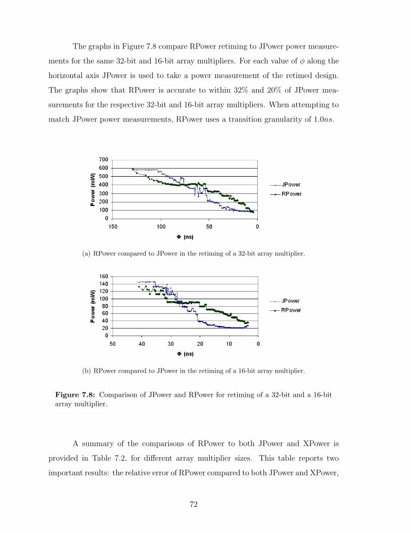
The graphs in Figure 7.8 compare RPower retiming to JPower power measure-
ments for the same 32-bit and 16-bit array multipliers. For each value of φ along the
horizontal axis JPower is used to take a power measurement of the retimed design.
The graphs show that RPower is accurate to within 32% and 20% of JPower mea-
surements for the respective 32-bit and 16-bit array multipliers. When attempting to
match JPower power measurements, RPower uses a transition granularity of 1.0ns.
(a) RPower compared to JPower in the retiming of a 32-bit array multiplier.
(b) RPower compared to JPower in the retiming of a 16-bit array multiplier.
Figure 7.8: Comparison of JPower and RPower for retiming of a 32-bit and a 16-bitarray multiplier.
A summary of the comparisons of RPower to both JPower and XPower is
provided in Table 7.2, for different array multiplier sizes. This table reports two
important results: the relative error of RPower compared to both JPower and XPower,
72

and also the power savings predicted by RPower through retiming. On average,
RPower is accurate to within 13% of XPower, and to within 17% of JPower. When
RPower uses a granularity of 0.35ns (to compare with XPower) it reports an average
power savings of 66% by retiming. When a granularity of 1.0ns is used (to compare
with JPower) an average power savings of 45% is reported by retiming.
Table 7.2: RPower’s average % error for different array multiplier designs comparedto XPower and RPower.
Operand RPower Average % Error % Power SavingsBitwidth XPower JPower 0.35ns gran 1.0ns gran
4 18.0 -12.6 33.3 10.28 12.2 5.4 65.4 37.516 7.4 31.7 78.2 57.432 12.5 19.5 91.6 76.0
An additional insight that Table 7.2 provides is that more power savings are
available from larger designs. Larger designs tend to have deeper delay paths. Glitch-
ing increases quadratically with depth[37], thus designs with deeper delay paths will
have more power savings available through glitch reduction. This observation was
also made in Chapter 4 with pipelining.
This chapter has shown that RPower can effectively estimate energy consump-
tion within FPGA designs. RPower estimates are within 13% of XPower post-place
and route power estimates, and within 17% of JPower power measurements. Since
RPower is an activation rate-based power estimation tool, it can be used at the gate
level to make FPGA architecture independent power estimations of any design.
This chapter has also shown that retiming can be used effectively to reduce
energy in FPGA designs. Retiming can reduce energy by up to 92%. An energy
evaluation metric called energy area delay has been shown to be an effective way to
weigh the power and clock rate improvements gained from retiming against the area
and latency costs. Using an algorithm combining retiming with RPower it is found
73

that for a set of testbench designs, an average of 40% energy reduction and a 54%
clock rate improvement can be gained at the cost of a 1.1× and 1.5× area and latency
cost respectively.
74

Chapter 8
Conclusion
This study has shown that retiming can be effectively used to reduce energy
consumption by up to 92%. Energy is reduced as retiming automatically pipelines and
repositions registers in order to reduce glitching. Without retiming, dynamic power
consumed from glitching can account for up to 97% of total power consumption in a
design. Retiming can almost eliminate glitching in a design.
This study has also shown that an energy metric called energy area delay is a
good way to explore the design space created by retiming. When this metric is used
with retiming for a set of testbench designs, the designs can be improved to consume
on average, 40% less energy and run 54% faster for only an average 1.1× area increase
and 1.5× latency cost.
An important part of retiming for power reduction is the activation rate-based
power estimation tool introduced in this study called RPower. RPower’s power esti-
mation capabilities are accurate to within 13% on average. The strength of RPower’s
power estimation comes from the transition probability model it is built on. RPower
estimates power by estimating transitions within a design. RPower accurately esti-
mates design transitions to within 10% on average.
Without requiring input vectors, LUT clustering, mapping, placement, or rout-
ing, RPower can estimate power for any design, for any FPGA architecture. Providing
relatively accurate power estimations to a retiming algorithm at the gate level means
that significant power reductions can be made early in the design process.
8.1 Future Work
In the future, RPower’s accuracy could be improved with the introduction of
a simple LUT clustering phase. A new clustering phase would simply ensure that
75

nodes within the retiming directed graph are grouped into 4-input LUTs. Currently,
some nodes represent only 2-input or 3-input LUTs. Thus the introduction of this
new LUT clustering phase would more closely match the actual FPGA mapping.
No architecture specific information would be necessary to perform this clustering,
so RPower’s accuracy would be improved while maintaining its relative architecture
independent status.
The algorithm in Chapter 7 that combines retiming with RPower can poten-
tially reduce the energy consumption of any FPGA design, however, it performs best
on feed-forward designs. Future work will improve upon this algorithm by catering
more to designs with feedback sections. Such improvements could include the use of
C-slow retiming techniques[58].
Additionally, the algorithm combining retiming with RPower will also be im-
proved by providing a better way to control the number of pipeline stages inserted into
a design. This improvement would allow this algorithm to interface with a synthesis
tool which has strict requirements for latency, throughput, and data introduction
levels.
The valuable power consumption information provided by RPower at such an
early stage in the design process could become an important part of a high-level
synthesis tool. Additionally, the information provided by RPower could be used as a
part of the algorithm used to technology map and place and route an FPGA design.
As the importance of low power consumption within digital designs grows, effective
power consumption estimation, early-on in the design process will become more and
more important to these kinds of tools.
Power consumption is becoming as important a design specification as area and
throughput in digital designs. In FPGA designs, which consume more power relative
to ASICs, this is especially true. Thus effective power evaluation and reduction
strategies are becoming more and more important. The gate level power estimation
and reduction techniques presented in this work are an effective way to address the
rising significance of power consumption reduction in FPGA designs.
76

Bibliography
[1] L. Stok and J. Cohn, “There is life left in ASICs,” in International Symposiumon Physical Design 2003 (ISPD’03). Proceedings, April 2003, pp. 48–50. 5
[2] E. Kusse and J. Rabaey, “Low-energy embedded FPGA structures,” in Interna-tional Symposium on Low Power Electronics and Design 1998, August 1998, pp.155–160. 5, 9, 10, 24, 26, 52, 83, 117
[3] F. Li, D. Chen, L. He, and J. Cong, “Architecture evaluation for power-efficientFPGAs,” in Proceedings of the 11th Annual International Symposium on Field-Programmable Gate Arrays (FPGA 2003), February 2003, pp. 175–184. 5, 11
[4] J. Kao, S. Narendra, and A. Chandrakasan, “Subthreshold leakage modeling andreduction techniques,” in IEEE International Conference on Computer AidedDesign. Proceedings, 2002, pp. 141–148. 5
[5] K. Usami, N. Kawabe, M. Koizumi, K. Seta, and T. Furusawa, “Automatedselective multi-threshold design for ultra-low standby applications,” in IEEEInternational Conference on Low-Power Electronics and Design. Proceedings,2002, pp. 202–206. 6
[6] T. K. et al, “A 0.9–v, 150–mhz, 10–mw, 4 mm2, 2–d discrete cosine transformcore processor with variable threshold voltage (VT) scheme,” JSSC, vol. 13,no. 11, pp. 1770–1779, Novmenber 1996. 6
[7] S. Narendra, A. Keshavarzi, B. Bloechel, S. Borkar, and V. De, “Forward bodybias for microporcessors in 130–nm technology generation and beyond,” JSSC,vol. 38, no. 5, pp. 696–701, May 2003. 6
[8] L. Clark, S. Demmons, N. Deutscher, and F. Ricci, “Standby power managementfor a 0.18µm processor,” in International Symposium on Low-Power Electronicsand Design. Proceedings, August 2002, pp. 7–12. 6
[9] S. Narendra, S. Borkar, V. De, D. Antoniadis, and A. Chandrakasan, “Scalingof stack effect and its application for leakage reduction,” in IEEE InternationalSymposium on Low-Power Electronics and Design. Proceedings, 2001, pp. 195–200. 6
[10] L. Shang, A. S. Kaviani, and K. Bethala, “Dynamic power consumption in virtex-ii FPGA family,” in Proceedings of the 10th Annual International Symposium onField-Programmable Gate Arrays (FPGA 2002), 2002, pp. 157–164. 6
77

[11] H. Veendrick, “Short-circuit dissipation of static CMOS circuitry and its impacton the design of buffer circuits,” JSSC, vol. 19, no. 4, pp. 468–473, August 1984.6
[12] F. Li, Y. Lin, L. He, and J. Cong, “Low–power FPGA using pre–defined dual–vdd/dual–vt fabrics,” in Proceedings of the 12th Annual International Sympo-sium on Field-Programmable Gate Arrays (FPGA 2004), February 2004, pp.42–50. 8, 11
[13] N. H. Weste and D. Harris, CMOS VLSI Design, 3rd ed. Boston, Massachusetts:Addison-Wesley, 2005. 8
[14] A. Shen, A. Kaviani, and K. Bathala, “On average power dissipation and ran-dom pattern testability of CMOS combinational logic networks,” in IEEE Inter-national Conference on Computer-Aided Design, 1992, pp. 402–407. 9, 27
[15] J. Leijten, J. van Meerbergen, and J. Jess, “Analysis and reduction of glitches insynchronous networks,” in European Design and Test Conference, 1995.ED&TCProceedings, March 1995, pp. 398–403. 9
[16] A. Raghunathan, S. Dey, and N. K. Jha, “Register transfer level power opti-mization with emphasis on glitch analysis and reduction,” IEEE Transactionson Computer-aided Design of Intergerated Circuits and Systems, vol. 18, no. 8,pp. 1114–1131, August 1999. 9, 10, 24
[17] K. S. Chung, T. Kim, and C. L. Liu, “A complete model for glitch analysis inlogic circuits,” Journal of Circuits, Systems and Computers, vol. 11, no. 2, pp.137–154, 2002. 9
[18] L. Benini, G. D. Micheli, A. Macii, E. Macii, M. Poncino, and R. Scarsi, “Glitchpower minimization by selective gate freezing,” IEEE Transactions on Very LargeScale Integration (VLSI) Systems, vol. 8, no. 3, pp. 287–297, June 2000. 9
[19] D. Kim and K. Choi, “Power conscious high level synthesis using loop folding,”in Proceedings of the 34th Design Automation Conference (DAC 1997), 1997. 9
[20] J. C. Monteiro and A. L. Oliveira, “Finite state machine decomposition for lowpower,” in Proceedings of the 35th Design Automation Conference (DAC 1998),1998. 9
[21] N. C. et al, “Unification of basic retiing and supply voltage scaling to minimizedynamic power consumption for synchronous digital designs,” in ACM GreatLakes Symposium on VLSI. Proceedings, 2003. 9
[22] Y. L. Hsu and S. J. Wang, “Retiming–based logic synthesis for low power,” in In-ternational Symposium on Low Power Electronics and Design 2002. Proceedings.ACM Press, 2002, pp. 275–278. 9
[23] T. Tuan and B. Lai, “Leakage power analysis of a 90nm FPGA,” in IEEE 2003Custom Integrated Circuits Conference. Proceedings, 2003, pp. 57–60. 10, 12
78

[24] J. Becker, M. Huebner, and M. Ullmann, “Power estimation and power measure-ment of Xilinx Virtex FPGAs: Trade-offs and limitations,” in Proceedings of the16th Symposium on Integrated Circuits and Systems Design (SBCCI’03). IEEEComputer Society Press, 2003. 10
[25] Y. Lin and L. He, “Leakage efficient chip-level dual–vdd assignment with timeslack allocation for FPGA power reduction,” in Proceedings of the 42nd DesignAutomation Conference (DAC 2005), June 2005, pp. 720–725. 11
[26] V. George, H. Zhang, and J. Rabaey, “The design of a low energy FPGA,” in In-ternational Symposium on Low Power Electronics and Design 1999. Proceedings,August 1999, pp. 188–193. 11
[27] F. Li, Y. Lin, and L. He, “FPGA power reduction using configurable dual–vdd,”in Proceedings of the 41nd Design Automation Conference (DAC 2004), June2004, pp. 735–740. 11
[28] ——, “Vdd programmabililty to reduce FPGA interconnect power,” inIEEE/ACM International Conference on Computer-Aided Design, November2004, pp. 760–765. 11
[29] Y. Lin, F. Li, and L. He, “Power modeling and architecture evaluation for FPGAwith novel circuits for vdd programmability,” in Proceedings of the 13th AnnualInternational Symposium on Field-Programmable Gate Arrays (FPGA 2005),February 2005, pp. 199–207. 11
[30] A. Gayasen, K. Lee, N. Vijaykrishnan, M. Kandemir, M. J. Irwin, and T. TUan,“A dual–vDD low power FPGA architecture,” in Field-Programmable Logic andApplications. Proceedings of the 13th International Workshop, FPL 2004, ser.Lecture Notes in Computer Science, LNCS 3203. Springer-Verlag, August2004. [Online]. Available: http://www.gigascale.org/pubs/596.html 11
[31] A. Lodi, L. Ciccarelli, and R. Giansante, “Combining low-leakage techniques forFPGA routing design,” in Proceedings of the 13th Annual International Sym-posium on Field-Programmable Gate Arrays (FPGA 2005), February 2005, pp.208–214. 11
[32] A. Gayasen, Y. Tsai, N. Vijaykrishnan, M. Kandemir, M. J. Irwin, and T. Tuan,“Reducing leakage energy in FPGAs using region-constrained placement,” inProceedings of the 12th Annual International Symposium on Field-ProgrammableGate Arrays (FPGA 2004), February 2004, pp. 51–58. 11
[33] J. H. Anderson and F. N. Najim, “Power-aware technology mapping for LUT-based FPGAs,” in IEEE 2002 Field-Programmable Technology (FPT) Confer-ence. Proceedings, December 2002, pp. 211–218. 12
[34] J. H. Anderson, F. N. Najam, and T. Tuan, “Active leakage power optimizationfor FPGAs,” in Proceedings of the 12th Annual International Symposium onField-Programmable Gate Arrays (FPGA 2004), February 2004, pp. 33–41. 12
79

[35] R. J. Francis, J. Rose, and A. Vranesic, “Fast technology mapping for lookuptable–based FPGAs,” in Proceedings of the 28th Design Automation Conference(DAC 1991), 1991, pp. 227–233. 12
[36] J. Cong and Y. Ding, “Flowmap: An optimal technology mapping algorithm fordelay optimization in lookup–table based FPGA designs,” IEEE Transactionson CAD, vol. 13, no. 1, pp. 1–12, 1994. 12
[37] M. Nemani and F. Najm, “Towards a high–level power estimation capability,”IEEE Transactions on CAD, vol. 15, no. 6, pp. 588–598, 1996. 12, 27, 73
[38] J. Lamoureux and S. J. E. Wilton, “On the interaction between power-awareFPGA CAD algorithms,” in ICCAD’03 Proceedings, 2003, pp. 701–708. 12
[39] S. J. Wilton, S.-S. Ang, and W. Luk, “The impact of pipelining on energy peroperation in field-programmable gate arrays,” in Field-Programmable Logic andApplications. Proceedings of the 13th International Workshop, FPL 2004, ser.Lecture Notes in Computer Science, LNCS 3203. Springer-Verlag, August 2004,pp. 719–728. 13, 23
[40] R. Fischer, K. Buchenrieder, and U. Nageldinger, “Reducing the power con-sumption of FPGAs through retiming,” in Proceedings of the 12th IEEE In-ternational Conference and Workshops on the Engineering of Computer BasedSystems (ECBS’05), 2005. 13
[41] XPower Manual, Xilinx, Inc. 15, 99
[42] U. East, “SLAAC-1V user VHDL guide,” Tech. Rep., 2004. 16
[43] P. E. Landman and J. M. Rabaey, “Architectural power analysis: The dualbit type method,” IEEE Transactions on Very Large Scale Integration (VLSI)Systems, vol. 3, no. 2, pp. 173–187, June 1995. 19
[44] A. Raghunathan, S. Dey, and N. K. Jha, “Register-transfer level estimation tech-niques for switching activity and power consumption,” in ICCAD’96 Proceedings,1996. 19
[45] S. Gupta and F. N. Najm, “Power modeling for high-level power estimation,”IEEE Transactions on Very Large Scale Integration (VLSI) Systems, vol. 8, no. 1,pp. 18–29, February 2000. 19
[46] T. Jiang, X. Tang, and P. Banerjee, “Macro-models for high level area and powerestimation on FPGAs,” in GLVLSI, April 2004, pp. 162–165. 19
[47] R. F. Lyon, “Two’s complement pipeline multipliers,” IEEE Transactions onCommunications, pp. 418–425, April 1976. 23, 30, 84
[48] Y.-N. Chang, J. H. Satyanarayana, and K. K. Parhi, “Systematic design of high-speed and low-power digit-serial multipliers,” IEEE Transactions on Circuits andSystems-II: Analog and Digital Signal Processing, vol. 45, no. 12, pp. 1585–1596,December 1998. 23
80

[49] B. E. Nelson, Designing Digital Systems, 1st ed. Provo, Utah: BYU AcademicPublishing, 2005. 25
[50] S. S. Demirsy, A. G. Dempster, and I. Kale, “Power analysis of multiplier blocks,”in IEEE International Symposium on Circuits and Systems, vol. 1, May 2002,pp. I–297–I–300. 26, 83
[51] J. Valls and E. Boerno, “Efficient FPGA–implementation of two’s complementdigit–serial/parallel multipliers,” IEEE Transactions on Circuits and Systems-II:Analog and Digital Signal Processing, vol. 50, no. 6, pp. 317–322, June 2003. 30,85
[52] U. Narayanan, P. Pan, and C. L. Liu, “Low power logic synthesis under a generaldelay model,” in International Symposium on Low Power Electronics and Design1998. Proceedings, August 1998, pp. 209–214. 34
[53] J. H. Anderson and F. N. Najm, “Switching activity analysis and pre-layoutactivity prediction for FPGAs,” in SLIP’03, April 2003, pp. 15–21. 48
[54] U. Narayanan, H. W. Leong, K.-S. Chung, and C. L. Liu, “Low power multi-plexer decomposition,” in International Symposium on Low Power Electronicsand Design 1997. Proceedings, August 1997, pp. 269–274. 49
[55] U. Narayanan and C. L. Liu, “Low power logic synthesis for XOR based circuits,”in International Conference on Computer-Aided Design 1997. Proceedings, 1997.49
[56] S. B. K. Vrudhula and H.-Y. Xie, “Techniques for CMOS power estimation andlogic synthesis for low power design,” in International Conference for Low PowerDesign 1997. Proceedings, 1994, pp. 21–26. 49
[57] C. E. Leiserson and J. B. Saxe, “Retiming synchronous circuitry,” Digital, Tech.Rep., August 1986. 59, 60
[58] N. Weaver, Y. Markovskiy, Y. Patel, and J. Wawrzynek, “Post-placement c-slow retiming for the xilinx virtex FPGA,” in Proceedings of the 11th AnnualInternational Symposium on Field-Programmable Gate Arrays (FPGA 2003),February 2003, pp. 185–194. 60, 76
[59] S. Xing and W. W. H. Yu, “FPGA adders: Performance evaluation and optimaldesign,” IEEE Design & Test of Computers, vol. 15, pp. 24–29, Jan-March 1998.84
[60] P. Bellows and B. Hutchings, “JHDL - an HDL for reconfigurable systems,” inProceedings of the IEEE Symposium on FPGAs for Custom Computing Machines(FCCM ’98), K. L. Pocek and J. M. Arnold, Eds., IEEE Computer Society.IEEE Computer Society Press, April 1998, pp. 175–184. 101
[61] EDIF manipulation software tool. BYU. [Online]. Available: http://reliability.ee.byu.edu/edif/ 102, 103, 109
81

[62] C. Carmichael, “Triple module redundancy design techniques for Virtex FP-GAs,” Xilinx Corporation, Tech. Rep., November 2001, xAPP197 (v1.0). 117
[63] N. Rollins, M. Wirthlin, and P. Graham, “Evaluation of power costs in apply-ing TMR to FPGA designs,” in Proceedings of the 7th Annual InternationalConference on Military and Aerospace Programmable Logic Devices (MAPLD),September 2004. 117
[64] R. Gonzalez and M. Horowitz, “Energy dissapation in general purpose micro-processors,” IEEE Journal of Solid-State Circuits, vol. 31, no. 9, pp. 1277–1284,September 1996. 122
82

Appendix A
Multiplier Designs
Multiplier designs are ideal for demonstrating the effects of glitching on to-
tal power consumption and on operation energy. A multiplier is a good design for
demonstrating this because of its large amount of net delays and varied net lengths
which lead to a large number of glitches[2, 50]. Two types of multipliers are shown
here: array multipliers and digit-serial multipliers. In most FPGA fabrics dedicated
multipliers exist. The array and digit-serial multipliers are not meant to replace
these dedicated multipliers, but are used to show the principle that reducing glitches
reduces power.
A.1 Array Multipliers
The multiplier in Figure A.1 shows that pipelining can be easily implemented
by adding registers between multiplier stages of an array multiplier. The 4x4 mul-
tiplier shown in Figure A.1 is one of the array multipliers used in this study. In
addition to this multiplier, 8x8, 16x16, and 32x32 array multipliers are used. Incre-
mental pipelining is applied to each of these multipliers. Multiplier designs begin as
non-pipelined (latency and throughput equal to one clock cycle), and pipelining is in-
crementally inserted until each design is fully pipelined (N pipeline stages for an NxN
multiplier). Pipeline stages increase by powers of two. So for the 32x32 multiplier,
the following number of pipeline stages are incrementally inserted: 0, 1, 2, 4, 8, 16,
and 32. Each pipeline stage is implemented by adding registers between multiplier
stages (Figure A.1) and is relatively equally spaced from other pipeline stages.
83

Figure A.1: 4x4 array multiplier.
Each multiplier stage is implemented as a carry-ripple adder. If implemented
in an ASIC, a carry-ripple adder may be a poor implementation, however, in an
FPGA it is the most efficient adder[59]. Xing and Yu show that compared to other
adders it has the lowest cost and highest performance-cost ratio. This is due to its
highly regular structure and effective use of CLB carry logic.
A.2 Digit-Serial Multipliers
The amount of pipelining available in the multiplier shown in Figure A.1 is
limited by number of multiplier stages. In other words an NxN multiplier can have
a maximum of N pipeline stages. Additional pipelining is available in a digit-serial
multiplier where pipelining is applied at a smaller granularity[47]. A digit-serial
multiplier is pipelined at the digit level. The increased pipelining leads to less glitches,
and therefore less power, but also leads to an increase in latency and throughput.
With such an extreme amount of pipelining the minimum clock period of the
digit-serial multiplier is reduced allowing for a faster clock rate, but the pipelining
not only increases the latency but also the throughput of the design. Whereas the
throughput of an NxN multiplier based on the design of Figure A.1 is one product per
cycle, the throughput of a digit-serial multiplier is one product per N/D cycles (where
D is the digit size). Note that for traditional digit-serial multipliers one product is
84

retrieved once per N ∗ 2/D cycles, but for this study we use an efficient digit-serial
multiplier that produces a product in half as many cycles[51]. New operands are
introduced to a digit-serial multiplier every N/D cycles.
Figure A.2: Signed digit-serial multiplier. The digit size is 2 and the operand bitwidthis 4.
Figure A.2 shows the design of a digit-serial multiplier with a digit size of two
and an operand bitwidth of four. The figure shows both a serial output and a parallel
output. The serial output produces the bottom half of the product, and the parallel
output produces the top half. The parallel output is only valid during the clock cycle
of the final serial output. This parallel output is what allows a data introduction rate
of N/D instead of N ∗ 2/D.
85

86

Appendix B
Using JPower
JPower is a tool that measures the amount of current flowing on the SLAAC1V
board. The ’J’ in JPower comes from Jason Zimmerman who made the tool opera-
tional while working at Los Alamos National Laboratories (LANL) during the summer
of 2003. The SLAAC1V board was originally designed with this current measuring
capability, but was not implemented in the SLAAC1V C API. In order to enable this
ability modifications were made to this SLAAC1V API and also to the SLAAC1V
XVPI controller. These modifications were intended for use using API 0.3.2, PCI
0.3.1 and XVPI 0.16.
The amount of consumed power this tool reports is a combination of both static
and dynamic power. Static power will be defined as the amount of power consumed
by a design when no clock is running. No signals will toggle on any of the nets of
a synchronous design when the clock is not running. Dynamic power on the other
hand refers to the amount of power consumed by active nets in the design. Transient
signals and glitches therefore add to the amount of dynamic power consumed by a
design.
B.1 SLAAC1V XVPI Changes
To update the SLAAC1V package enabling the JPower tool functionality the
XVPI controller must be reprogrammed with the modified XVPI controller. The
bitfile required to reprogram the XVPI EEPROM must be obtained from LANL or
BYU. Before reprogramming the XVPI controller it is essential to ensure that the
87

SLAAC1V board is not in use. It is also wise to ensure that no intensive programs
are running on the computer hosting the SLAAC1V board. The following procedure
can be followed to reprogram the XVPI EEPROM:
1 Change to the directory: $SLAAC1V ROOT/pub/bit/xvpi
2 Run: ../bin/slaac1vdb
3 In the debugger run the command:
eeprom write xvpi1v continuous adc cclk.bit
4 Quit the debugger
5 SHUTDOWN the computer (do not simply reboot)
6 After turning on the computer repeat steps 1 and 2
7 In the debugger load any design into XP1: conf x1 <bitfile>
8 In the debugger run the command: rc 0x6a
If the register value reported is 0x1fffff the XVPI reconfiguration did not work.
If the reconfiguration did work, the register value reported will most likely be:
0x1fff20.
9 Another way to test to see if the XVPI reconfiguration worked is attempt to
write to register 0x6a: wc 0x6a 0x1fff2c
Note that only the last 10 bits of the register are writable.
It is important to note that this procedure only needs to be performed once.
After successfully reprogramming the XVPI EEPROM, it should not have to be done
again.
88

B.2 JPower Details
The SLAAC1V board current is measured by means of the analogue to digital
converter (ADC). The SLAAC1V board ADC is then used to sample the current from
one of three different channels. Channel 0 reports the 5V current, channel 1 re-
ports the 2.5V current and channel 2 reports the 3.3V current. Since the SLAAC1V
board contains Virtex XCV1000 chips, channel 2 reports the I/O current, and chan-
nel 1 reports the current drawn by the rest of the chip logic. The ADC can sample a
single channel at up to 120 kHz or can sample multiple channels at a rate of 120 kHz
divided by the number of channels being sampled. In most cases the only channel
that will be sampled will be channel 1.
When the ADC samples a channel, the value sampled is recorded in a regis-
ter on the SLAAC1V board (register 0x6A) as a 10-bit number. To transform this
10-bit number into a current measurement, the register value is multiplied by a con-
stant (4.8828125) and rounded to produce a current value in mA. Measurements can
therefore be taken in the range of 0 to 4990 mA.
B.3 SLAAC1V API Additions
In order to access the values reported by the SLAAC1V board ADC, additions
were made to the SLAAC1V C API. New data types and functions were added to
the SLAAC1V API files called Slaac1VBoard.h and Slaac1VBoard.c in order to
facilitate the use of JPower.
B.3.1 API Structure Additions
The following C struct was added to represent the different channels:
struct CHANNEL_STRUCT {
int ch0;
int ch1;
89

int ch2;
int ch3;
};
Each integer represents the corresponding channel indicated by its name. Channel 3
is not currently functional.
A channel mask is an important parameter in many of the ADC functions
(which will be named channel mask). This mask is of type UINT (a previously
defined SLAAC1V API type) and is initialized to be a boolean OR of a combination
of the following newly defined constants:
• ADC CH 0 (or ADC 5V CH)
• ADC CH 1 (or ADC 2 5V CH)
• ADC CH 2 (or ADC 3 3V CH)
• ADC CH 3
When the SLAAC1V board ADC is powered down a parameter is passed to
the function that performs this task. The parameter (which will be named pd mode)
is one of the values defined by the following enumeration:
typedef enum _ADCPowerdownMode {
ADC_FULLPD=0,
ADC_FASTPD=1,
ADC_NOPD=2 } ADCPowerdownMode;
B.3.2 API Function Additions
In order to gain access to the SLAAC1V board’s ADC a few basic functions
were added to the SLAAC1V API. The following functions have been added to to
enable the use of JPower:
90

• void ADCStart(UINT channel mask);
– This function starts the continuous ADC circuit with the channels enabled
specified by the channel mask. Remember that the ADC can only be
sampled at 120 kHz divided by the number of channels in the channel
mask.
• void ADCStop();
– Stops the ADC.
• void ADCPowerdown (ADCPowerdownMode pd mode);
– Provides power down control for the ADC. This function should be called
at least 12.77 µs before ADCStop().
• int ADCRead (UINT channel mask, struct CHANNEL STRUCT*
channels);
– Reads a sample from the given channels and returns a value rounded to
the closest mA. Returns -1 if any of the channels draw more than 4990
mA.
B.4 JPower Sample
In order to show how JPower works, a simple design is used whose current
can be easily measured. If a design is too small it is difficult to accurately measure
the amount of current it uses. The design used in this example is large enough to
enable accurate current measurements. The array of 72 8-bit incrementers shown in
Figure B.1 acts as a simple design. The incrementer is replicated so that the design
will consume enough dynamic power for JPower to accurately measure. The bitwidth
of the incrementers is restricted to 8 so that the nets in the design will be relatively
active.
91

Figure B.1: Test design - an array of 72 8-bit incrementers
To measure the amount of current flowing in the SLAAC1V board the SLAAC1V
C API is used. Once a bitstream for the array of incrementers has been created to
place in XP1, the API is used to load the SLAAC1V board and control the ADC. To
take a current measurement from the design the following code could be run in a C
file:
.
.
.
CHANNEL_STRUCT chan;
UINT channel_mask = ADC_2_5V_CH;
Slaac1VBoard board = new Slaac1VBoard(NULL, xp1_design, NULL);
board->ADCStart(channel_mask);
board->run();
wait(wait_time);
board->ADCRead(channel_mask, &chan);
board->ADCPowerdown(ADC_FULLPD);
wait(wait_time);
board->ADCStop();
.
.
92

The problem with just running this set of functions to get a power measure-
ment is that the measured result is not consistent every time it is run. When it is run
just once there may be a power spike right when the current is sampled. On the other
hand the design could be at it’s lowest power usage at that moment. To eliminate
the effects of such extreme measurements, an average of many measurements should
be taken. To illustrate this, Table B.1 shows current measurement results when this
simple program is run five times in a row (with a clock frequency of 20 MHz). The
table shows that when the current is sampled only once the results vary from as low
as 444 mA up to 537 mA (column 2). On the other hand, instead of sampling the
current just once each time the program is run, the current should be sampled a
number of times. When a number of samples are taken each time the program is run
the averaged current varies only from 488 mA to 490 mA (column 3).
Table B.1: JPower current measurements for an array of 72 8-bit incrementers -single sampling and averaged sampling
Trial Single (mA) Averaged (mA)
1 444 488.22 513 489.43 474 489.34 449 490.05 537 488.8
In order to get consistent power measurement results the channel is sampled
many times and all of the measurements are averaged. Column three of Table B.1
shows the results from sampling the 2.5V channel 5000 times and averaging the mea-
surements (again the SLAAC1V clock is run at 20 MHz). From this point forward
when current is measured using JPower it is assumed that the 2.5V channel is sampled
5000 times and the measurements are averaged.
93

B.5 JPower Calibration
The amount of current reported by JPower includes the current flowing through
the entire SLAAC1V board and not just the design on the XP1 FPGA. This means
that the measured current flowing in the array of incrementers (Figure B.1) is lower
than the amount listed in Table B.1. There needs to be a way then to find what
portion of the current sampled by the ADC is flowing through the designs in the XP1
FPGA. There are many other resources on the SLAAC1V board besides this single
FPGA chip where the design resides. Each of these resources also consume power.
These resources include the other two FPGA chips on the board (X0 and XP2), the
XVPI EEPROM controller, the 12 MB of on-board memory, the two on-board FIFOs,
and the PCI connection.
To distinguish between the current flowing through the XP1 FPGA and the
current flowing through the rest of the SLAAC1V board some tests were run on the
board with no designs present on any of the FPGAs (except that when no design is
loaded into X0, a default design is loaded). With no designs present on the SLAAC1V
board, the ADC was used to sample the current flowing through the board when it was
run at a range of different frequencies (0 to 70 MHz). These tests were first run with
the clock turned off and then with the clock turned on. The resulting measurements
are found in Table B.2.
From the results found in Table B.2 the slope and intercept of each column
(shown in Figure B.2), can be used to create an equation for the current in terms of
whether the clock is turned on as well as frequency. This equation follows:
BASE CURRENT = 315 + FREQ + CLK ∗ (3FREQ) (B.1)
94

Table B.2: ADC sample results of the 2.5V channel when no designs are present onthe SLAAC1V board
Freq (MHz) No CLK (mA) CLK (mA)
10 322 35020 330 38530 337 42040 344 45550 352 49360 358 52770 366 564
where
FREQ = clock frequency (in MHz), and
CLK =
0 : no clock running
1 : clock running.
Equation B.1 is divided into to two parts: static and dynamic current. The
CLK variable marks this delineation. It is interesting to note that the static current
is somewhat dependent on the frequency at which the design clock runs. This de-
pendence is shown by the slope of the non-clocked current in Figure B.2. A flat line
would have indicated no dependence on the clock frequency. The y-intercept of this
slope is where the static current constant (315) is derived.
The second part of the equation in Equation B.1 represents the dynamic cur-
rent. The graph of the clocked current measurements in Figure B.2 has the static
current included as a part of its measurements. Therefore, in order to decipher the
amount of dynamic current, the static current measurements must be subtracted from
the clocked measurements. Subtracting the slope of the non-clocked measurements
from the clocked measurements reveals the dynamic current (the 3FREQ variable in
Equation B.1).
95

Figure B.2: Calibration slopes for JPower
Equation B.1 can be applied to the current values in Table B.1 to find out
how much current to subtract from these original measured current values. Since the
values in Table B.1 were obtained when the board was run at 20 MHz, the value 20
is substituted for the FREQ variable. Also, since the clock was running when those
values were obtained, the value 1 is substituted for the CLK variable. The amount
of current to be subtracted is:
BASE CURRENT = 315 + (20) + (1) * (3(20))
= 395 mA.
Subtracting this amount of current from the values in Table B.1 shows the
actual current measurements for the array of 72 8-bit incrementers. These values are
shown in Table B.3 (compare with the values in Table B.1).
JPower’s ability to take true power consumption measurements for a design is
invaluable. Unfortunately however, since the JPower tool is linked to the SLAAC1V
board, it’s use is limited to designs based on Xilinx’s Virtex FPGA architecture.
96

Table B.3: Single sampled and multiple average sampled current measurements foran array of 72 8-bit incrementers
Trial Single (mA) Averaged (mA)
1 49 93.22 118 94.43 79 94.34 54 95.05 142 93.8
97

98

Appendix C
Using XPower
The amount of power dissipation this tools reports is a combination of both
static and dynamic power. Static power will be defined as the amount of power
consumed by a design when no clock is running. No signals will toggle on any of
the nets of a synchronous design when the clock is not running. Dynamic power
on the other hand refers to the amount of power consumed by active nets in the
design. Transient signals and glitches therefore add to the amount of dynamic power
consumed by a design.
Xilinx has a power estimation tool called XPower[41] which can estimate power
consumption of designs for a variety of Xilinx FPGA architectures (not just Virtex).
This tool is different from JPower in that it does not measure the actual current
flowing in an FPGA. Instead, based on the input design, it calculates a power con-
sumption estimate. This estimation is based on the design resources as well as the
activity rates (the number of transitions) of the nets in the design. In order for
XPower to be able to perform this estimation, every net in the design must have an
activity rate assigned to it.
The signal activity rates of design nets must be imported into XPower inde-
pendently of the placed and routed FPGA design. Xilinx provides three different
ways to import this information. The first method to import net activity rates is to
individually set each rate by means of the graphical XPower tool. Setting every net’s
activity rate this way is unrealistic since a design can have thousands of nets. The
next method imports activity rate information through a ModelSim simulation file (a
99

VCD file). The third way to import this information is by means of an XPower XML
settings file.
Regardless of which method is used to import activity rate information, XPower
will report the confidence level of it’s power estimation, along with the percentage of
nets which have activity rates set. When all of the nets have activity rates assigned
to them, XPower reports an accurate confidence level. If some of the nets do not have
activity rates assigned to them, the confidence level is reported as reasonable, and if
a significant number of nets do not have an activity rate assigned to them XPower re-
ports an inaccurate confidence level. Regardless of which activity rate setting method
is used, an accurate XPower confidence level is important.
Figure C.1: Example of an XPower confidence level report
100

Figure C.1 shows an example of an XPower confidence report. Outlined with
a yellow box in the figure is the XPower button that will report the power estimation
confidence level. Outlined with the green box is the confidence level report. In this
example none of the design nets have activity rates set and so a confidence level of
inaccurate is reported.
Figure C.1 shows the graphical XPower tool. XPower can also be run from
the command line using the xpwr command. Both ways of running XPower can give
more information than simply a power consumption estimate. As well as a current
and power consumption estimate for every signal, loading information can also be
provided. To write this information to a file the following switches must be used
along with the xpwr command: -v -a -l <file size>. The -v switch means verbose
and the -a switch prints out an advanced report. The -l switch sets a maximum file
size for the report. Just like the graphical XPower tool, the command line version
will also indicate either an inaccurate, reasonable, or accurate confidence level.
An accurate XPower confidence level is important for a reliable power esti-
mation, however an accurate confidence level in and of itself will not guarantee a
reliable estimation. An accurate timing model must be used to generate the net ac-
tivity rate information before it is imported by XPower. This must be taken into
account whether a ModelSim simulation file (VCD file) or an XPower XML settings
file provides the activity rate information to XPower.
C.1 XPower Static Simulation Using XML Setting Files
XPower can create XML files as a means of saving session settings. An
XPower-created XML file can therefore be loaded to restore the settings of a pre-
vious XPower session. Since XML files can be created by XPower to restore settings,
XML files can also be created independently of XPower to provide settings. JHDL[60]
can be used to create such an XML file. A JHDL simulation can be used to collect
the transition rates of all the nets in a design and then write that information into an
101

XML file that is readable by XPower. This power simulation flow is shown if Figure
C.2. Note that although a JHDL testbench is used to gather transition information
to create an XML file, the original design need not be written using JHDL. An EDIF
tool exists which can import the EDIF created from any HDL and generate a JHDL
wrapper to interpret the EDIF design as a JHDL design [61]. This JHDL wrapper is
then used in the testbench to create an XML file.
Figure C.2: Static XPower simulation flow using JHDL
A JHDL-created XML file successfully assigns the activity rates to every net
of a design (and therefore achieves an accurate XPower confidence level), however
JHDL is unable to simulate transient signals. Since JHDL is unable to simulate
glitch signals, the activity rates produced are too low, resulting in inaccurate XPower
power estimation reports. This study goes on to show that for some simple designs the
estimations based on this JHDL static simulation can be off by up to 26%. Because
of this inaccuracy, importing activity rate information through ModelSim simulations
is considered to be a more accurate method for power consumption estimation.
102

C.1.1 HDL to XPower Name Conversion
When using a JHDL testbench to create an XML settings file usable by
XPower, it is essential that the net names are in a format recognizable by XPower.
This means that some of the net names seen in the JHDL testbench will need to be
altered. There are a few changes that need to be made to JHDL testbench net names
before they are recognized by XPower.
The first net name alteration changes net names within a bus. In the JHDL
testbench the individual nets within the bus are delimited with angle brackets: “<”
and “>”. For example the sixth net in a bus called ‘x’ would be represented as:
“x<5>”. For XPower to recognize this net, the angle brackets need to be replaced.
The angle brackets need to be replaced by one of two representations: normal brackets
“(” and “)” (if the original design was written in VHDL), or token versions of the
angle brackets “<” and “>” (if the original design was written in JHDL).
The second modification requires that name hierarchy be removed from the net
name. For example, the JHDL testbench net name “arraymult/un22 temp axb 6”
would have to be truncated to “un22 temp axb 6”.
The biggest change to the JHDL testbench net name must be made with the
help of the EDIF tool previously mentioned [61]. Within an EDIF file sometimes
a net will be renamed. In this case a net has an old name and a new name (the
renamed name). XPower uses old names for nets, not the new name created in EDIF.
The EDIF tool previously mentioned must be used in conjunction with the JHDL
testbench to find the old net names and use them.
Along with using old EDIF net names, some final changes must be made to
some net names. As an example of one such change, some of the nets that are re-
named in EDIF contain the string: “cryZ0Z” (the “Z0Z” portion does not exist in
the old name). To the old name of these nets must be appended the string: “ 0/O”.
For example, a net with the new EDIF net name, “un22 temp cryZ0Z 2” has an old
103

name, “un22 temp cry 2” but XPower recognizes the name as, “un22 temp cry 2 0/O
”. The EDIF tool previously mentioned can be used to make this and all other nec-
essary net name modifications, so that all net names will be recognized by XPower.
With these modifications the JHDL testbench net names will be suitable for
XPower. If there are any discrepancies, offending net names will be listed in XPower
reports.
C.2 XPower Dynamic Simulations Using ModelSim VCD Files
In order to demonstrate how ModelSim can be used to produce accurate tim-
ing information, another simple test design is introduced. A series of 416 up/down
loadable counters (shown in Figure C.3) will be used as another test design.
Figure C.3: Series of 416 up/down loadable counters
C.2.1 Capturing Transient Signals
Xilinx tools can be used to create timing information (SDF file) from a given
design, which takes into account transient signals (glitches). This back-annotated
timing information can be imported into ModelSim along with a VHDL design to
create an accurate simulation file (VCD file) needed by XPower. This simulation
file not only produces an accurate XPower confidence level but is also based on an
accurate timing model. As a result, reliable power estimation reports are produced.
The tool flow for using ModelSim to accurately simulate dynamic power is shown in
Figure C.4.
There are a few important procedures to follow when creating VCD files with
ModelSim for use in XPower. To begin with, a flattened VHDL design is required to
104

Figure C.4: Dynamic XPower simulation flow using ModelSim
import to ModelSim. The design must be flattened because XPower cannot handle
hierarchy within VCD files. If there is no hierarchy in the VHDL design, there will
be none in the VCD file.
Regardless of what hardware description language (HDL) is used to create the
FPGA design, a flattened (i.e. flattened in terms of hierarchy) VHDL design can be
back-annotated using a simple Xilinx command (this also means that the HDL code
does not have to be written without hierarchy). To begin with, simply synthesize
the design using the Xilinx tool flow (up to a placed and routed design). Next use
the Xilinx back annotation command called netgen as follows: netgen -sim -ofmt
vhdl -fn <design name>.par.ncd. The -sim option indicates that a simulation
output is desired. The -ofmt vhdl parameter indicates that the back annotated
output file will be in VHDL format. The -fn option indicates to create a flattened
VHDL design. Note that there are other netgen options that can be used that may
be applicable.
Another important aspect of accurate timing information is the timing infor-
mation provided by an SDF file. This file is created in the back annotation process by
105

the Xilinx tools. When this file is used by means of the -sdfmax option in ModelSim,
more accurate results are obtained in XPower since transient signals are taken into
account.
Now with a flattened VHDL file and a back annotated timing file (SDF file)
ModelSim can be used to create a VCD file for XPower. Using ModelSim this way
provides important transient signal information (glitches) - something that the XML
method did not provide. In order to get transient signal information the timing reso-
lution must be sufficiently small. This can be done with the -t option in ModelSim.
This option takes a time value as an argument (ex: -t 10ps). For optimal results it
is suggested that a granularity of 1 ns be used. A smaller granularity will capture
more simulated glitching, however many of those glitches are unrealistically small and
would not likely be produced in hardware. Thus a larger granularity acts to filter out
these smaller glitches.
Figure C.5 shows the wave form produced in ModelSim by a simulation of the
example design from Figure C.3. The yellow box in the figure highlights some signal
glitches. Remember that using XML files as a way of importing signal information
to XPower does not include glitches. As this figure shows, glitches can be quite
prevalent.
C.2.2 Input Vectors
The next important step toward obtaining an accurate XPower confidence
level report is to ensure that all of the FPGA design inputs are driven with input
vectors during the ModelSim simulation. Doing this should ensure that all of the nets
in the design are active during the simulation. This also means that the ModelSim
simulation must run long enough to capture a sufficient amount of net activity. If
the simulation is not run long enough some or many nets in the design will have low
or zero activity rates - leading to a reasonable or an inaccurate confidence report in
XPower.
106

Figure C.5: Waveform from a ModelSim simulation of the design in Figure
To provide the stimuli for the design inputs a ModelSim DO file can be used.
Since the example design used here contains only counters, there are very few inputs.
DO files can be written using TCL so when there are a large number of inputs to be
driven, input vectors can be read in from files using TCL commands. The following
lines are an example of what can be used in such a DO file:
vlib work
vcom <design>.vhd
vsim -sdfmax <design>.sdf -t 10ps <design>
force <design>/clk 0,1 10ns -r 20ns
force <design>/reset 0
vcd file <design>.vcd
vcd on
vcd add <design>/*
run <design_time>
107

vcd flush
quit -f
With a back-annotated VHDL file, an SDF file and a DO file, ModelSim can
be effectively used to create a VCD simulation file. It is important to note that VCD
files can be very large (over 1GB). XPower will not recognize VCD files that are too
large (greater than about 1.5 GB). In order to limit the size of VCD files, the -limit
option can be used in the DO file.
C.2.3 EDIF to XPower Name Conversion
Sometimes some of the flattened VCD net names are not written in a format
that XPower can recognize. When XPower cannot recognize a net from the VCD file
it will not be able to include power consumption information from that net. To find
out if there are any nets that XPower could not get information about, the estimate
activity rates option in XPower can be used. Figure C.6 shows the results of using
this option. The yellow box shows the estimate activity rates button and the green
box shows that after pressing this button a file called <design name>.parfield.txt is
created which lists the nets which have no activity rate (where <design name> is the
name of the design).
Often the nets listed in the <design name>.parfield.txt file are indeed included
in the VCD file, but the name format of the VCD net name is not the format XPower
expects. When this is the case, performing a search in the VCD file for the nets in
the <design name>.parfield.txt file will reveal the discrepancies in net name formats.
Often the problem is that some of the underscores ‘ ’ in the VCD file net name should
be replaced by double underscores ‘ ’. Also in some cases an underscore ‘ ’ needs to
be replaced by a forward slash ‘/’. For example, in the XPower estimation in Figure
C.6 The VCD net name: “upcntnohalflatch 103 muxcy l 5 o” was modified to
become “upcntnohalflatch 103/muxcy l 5/o”. As described in the HDL to
108

Figure C.6: XPower activity rate estimation example
XPower Name Conversion section, an EDIF tool [61] can be used to correct these
net names.
C.3 XPower XML Method vs. VCD Method
If XPower reports an accurate confidence level and XPower’s activity rate
estimator option reveals no nets with missing activity rate information then accurate
XPower results may not be far behind. Remember that these two things alone will
not guarantee accurate results. Again the importance of using accurate timing models
must be emphasized. Using the static simulation JHDL/XML method of specifying
activity rate information can produce an accurate confidence level report and report
no nets with lacking activity rate information in XPower. However, the XML method
cannot provide important transient signal information. Transient signals (glitches)
cause a significant amount of power consumption.
To show how significant the transient signal information is that VCD files
provide, compare the XPower results for some test designs using both methods. The
109

Table C.1: Comparison of XML and VCD methods
Incrementers Up/Down CountersFreq XML VCD Diff %Err XML VCD Diff %Err
(MHz) (mW) (mW) (mW) (mW) (mW) (mW)
10 56 64 8 14.3 222 260 38 17.120 85 103 18 21.2 418 494 76 18.230 115 142 27 23.5 614 727 113 18.440 145 180 35 24.1 818 960 142 17.450 175 218 43 24.6 1006 1188 182 18.160 205 257 52 25.6 1202 1419 217 18.170 235 295 60 25.5 1399 1649 250 17.9
two example designs will be used for this purpose (Figures B.1 and C.3). Both designs
will be simulated with each method, at a range of different frequencies. Table C.1
compares the results of these two methods. Note that the power reported in this table
is the power from the 2.5V source and not the total power estimation. Only the 2.5V
power is reported so that comparisons can be made with JPower results. Also, these
results are for a Virtex XCV1000 chip (again, so that the results can be compared
with JPower).
Table C.1 shows that without transient signal information the estimated power
consumption is about 24% less than with transient signal information for the array of
incrementers, and about 18% less for the series of up/down loadable counters. This
indicates that glitches account for a significant amount of power consumption.
In order to test what other factors could affect XPower results a series of
tests were done using these same two example designs (Figures B.1 and C.3) in
which different XPower parameters were varied. In particular, the temperature and
voltages were varied. Varying the XPower temperature parameter had no effect on
the estimated power results. Varying the value of the 2.5V source however did have
an effect. For each 0.1V variation from the 2.5V voltage there was about a 4% change
in the current estimation.
110

Appendix D
Comparing JPower and XPower
The amount of consumed power these tools report is a combination of both
static and dynamic power. Static power will be defined as the amount of power
consumed by a design when no clock is running. No signals will toggle on any of
the nets of a synchronous design when the clock is not running. Dynamic power
on the other hand refers to the amount of power consumed by active nets in the
design. Transient signals and glitches therefore add to the amount of dynamic power
consumed by a design.
Having two different tools to evaluate power consumption, ideally both tools
will produce similar results. JPower measures actual current values, but must be
calibrated. XPower only estimates power consumption and must be properly fed
with everything it needs for accurate results. In this section the results of the two
tools are compared.
Before comparing results of the tools, the test designs that have been used will
be described in more detail. Figure B.1 shows a high level view of an array of 72 8-bit
incrementers. Figure D.1(a) shows the details of a single bit incrementer. As the
figure shows, the incrementer easily fits within a single slice of a CLB. It is difficult
for the tools to precisely measure the power consumption of an 8-bit incrementer (let
alone a single-bit incrementer). For this reason an array of incrementers is used.
72 incrementers are used so that each incrementer output can be fed to an
IOB on the SLAAC1V board. Connecting the most significant bit of each incrementer
output to an IOB prevents the design from being optimized away. Since I/O is limited
111

(a) Details of a single-bit incrementer (b) Details of a single-bit up/down loadablecounter
Figure D.1: Single-bit incrementer and up/down loadable counter used as test designsto compare XPower and JPower results.
on the SLAAC1V board, so is the number of 8-bit incrementers that can be included
in the array. In this study the collection of IOBs on the XP1 chip which correspond to
the Left bus are the IOBs used for output signals. Since the Left bus is 72 bits wide,
the incrementer can be replicated only 72 times. In order to ensure that the nets of
the incrementers remain relatively active, the bitwidth of each replicated incrementer
is limited to 8 bits.
Figure C.3 shows the high level diagram of the series of 416 up/down loadable
counters. Figure D.1(b) shows the details of a single-bit up/down loadable counter.
Just like the single-bit incrementer, the single-bit counter fits within a single slice of
a CLB and so in order to provide a design which consumes a significant amount of
power, the counter is replicated. The output of each replicated counter is fed into the
load input of the next replicated counter, producing a long string of counters. The
output of the last counter leads to IOBs. Note that this design is not I/O limited like
the array of incrementers is. This means that the counter can be replicated as many
times as the Xilinx place and route tool will allow for Virtex XCV1000 chip.
To provide a third test design, the array of incrementers from Figure B.1 is
used and a way is provided to replicate the incrementers more than just 72 times. As
Figure D.2 shows, the incrementer outputs are sectioned into groups of 16. Within
112

a group, the most significant bit of each incrementer is fed into an XOR gate, which
then leads to an IOB. This allows the 8-bit incrementer to be replicated 416 times.
Figure D.2: An array of 416 8-bit incrementers with grouped outputs leading to XORgates
With these three test designs the results of JPower and XPower are compared.
These comparisons are made using both tools to measure and estimate the power
consumption of each design when run at a range of different frequencies. Taking
power measurements at a range of frequencies provides a plot of frequency vs. power
(energy) from which a slope can be interpolated which has units of mW per MHz
(nJ). This slope corresponds to the dynamic power consumption. The intercept of
this line provides a value for the static power. Figures D.3, D.4, and D.5 show the
results of this test graphically and Table D.1 provides the numbers.
Table D.1: Comparison of JPower and XPower for the three test designs
Incr XOR Cnt
Static Power (mW)JPower 12.5 18.6 17.9XPower 26.4 30.4 31.4
Dynamic Power (nJ)JPower 3.8 19.6 27.7XPower 3.8 19.9 23.1
113

Figure D.3: JPower and XPower plot for an array of 72 8-bit incrementers
Figure D.4: JPower and XPower plot for 416 XOR’ed 8-bit incrementers
The table and graphs show that overall JPower and XPower match up quite
well. There are deviations however. These differences could indicate a problem with
the JPower measurements, with the XPower estimations or a combination of both.
The JPower calibration equation could need to be altered under some circumstances.
The difficulties of using XPower properly are discussed in the XPower appendix.
114

Figure D.5: JPower and XPower plot for 416 8-bit up/down loadable counters
115

116

Appendix E
The Effects of Placement and Routing on Power
The interconnect of an FPGA accounts for the majority of the area on the
chip and also accounts for the majority of the power dissipated by FPGA designs [2].
The amount of power consumed by the interconnect and clock tree can account for
up to 86% of total dissipated power [2]. Effective use of the interconnect therefore is
essential to minimizing power consumption.
Misuse or ineffective use of FPGA interconnect can cause significant increases
in power consumption. Previous studies relating to power costs of triple modular
redundancy (TMR) on FPGAs [62] have shown that a poorly placed design can cost
over 2x more in terms of power than a well placed design [63]. The study of the
effects of TMR on power consumption for FPGAs was performed by the author of
this document and a part of that study will follow.
To demonstrate the effects of placement and routing on power consumption
of FPGA designs, TMR is first applied to the simple incrementer design in Figure
B.1. Applying TMR triples the design’s size (in terms of LUTs). After the design
is triplicated, four different placement schemes are applied to the design. The first
placement is the auto-placement done by the Xilinx place and route tools. The
remaining three placements are hand placements done as shown in Figure E.1. The
first of these three hand placements is a poor placement; the incrementers are spread
far apart from each other and therefore long nets are required to connect to the voters.
The second placement is an improvement on the first, but the third placement is the
best placement.
117

Figure E.1: Three different hand placements of the array of 72 8-bit incrementersafter TMR has been applied.
Table E.1 lists the energy slopes (similar to those shown in Table D.1) for the
four different placements for both the JPower and XPower tools. It also lists the same
slopes normalized to the ideal placement (hand placement 3). The normalized values
show how power consumptions is related to placement. It also shows that JPower
is more sensitive than XPower to design placement. For the poor hand placement
JPower reports an energy slope of 10.65 nJ while XPower reports 6.20 nJ. Notice
however that for the ideal placement both XPower and JPower differ by less than
1%.
Table E.1: Relative power costs for different placements of an array of 72 8-bitincrementers
IncrementerAuto-Place Place 1 Place 2 Place 3
Energy Slopes (nJ)
JPower 7.37 10.65 6.15 4.76XPower 5.23 6.20 5.21 4.78
Normalized Energy Slopes
JPower 1.55 2.24 1.29 1.00XPower 1.09 1.30 1.09 1.00
118

Appendix F
Power and Energy Metrics
Most studies quantifying the power consumption of FPGA circuits report on
the average power of the overall circuit. More often however, the primary concern
is the amount of energy consumed. Energy can be a more useful metric since it is
not dependent of operating frequency. The energy consumption of the individual
operators and modules within a design can be individually evaluated to build low-
energy design. In other words, understanding the energy consumption of individual
operators will allow the designer or synthesis tool to choose operators that meet a
specific throughput constraint while minimizing energy consumption. In this chapter,
four different energy parameters are used: energy per operation, energy delay, energy
throughput, and energy density.
F.1 Energy per Operation
Energy per operation quantifies the amount of energy required to complete
a single operation of a specific circuit operator. This measure, reported in nJ, is
more useful than an average power measure when comparing arithmetic circuits with
different implementation approaches. Specifically, this measure allows us to compare
the energy efficiency of multi-cycle operators with single-cycle operators.
Circuit energy can be computed by integrating the circuit power consumption
over time (E =∫
Pdt). Assuming constant power consumption, the energy can be
estimated by multiplying the average power of the circuit operator by the amount
of time to complete a single operation. For single-cycle operators, the energy per
119

operation is simply the average power of the circuit times the clock period:
Ecycle = P · tclk (F.1)
where
P = the average power of the circuit, and
tclk = the circuit clock period.
The pipelined array multiplier (Appendix A) is an example of a circuit with
a single-cycle operation. The energy per operation for the pipelined multipliers is
shown in Figure F.1. Energy per operation is affected by glitching power. Just as the
graph of power consumption in Figure 4.5 drops logarithmically, Figure F.1 shows
that energy per operation also drops logarithmically. The graph also shows that as
the width of the multiplier increases, energy per operation grows exponentially.
Figure F.1: The energy per operation (in nJ) for an array multiplier of different widthsand various amounts of pipelining.
The energy per operation of multi-cycle circuit operators must take into con-
sideration the number of clock cycles required to perform the operation. For a non-
120

pipelined multi-cycle operator, the energy per operation is:
Eop = P · tclk · n (F.2)
where
P = the average power of the circuit,
tclk = the circuit clock period, and
n = the number of clock cycles required to perform the operation.
Pipelined operators overlap the computation of several discrete operations in
a single clock cycle. The energy consumed by a pipelined operator is shared among
the various instances of the operator in the pipeline. Thus for pipelined operators,
rather than considering the number of cycles required to perform the operation (n),
the interval between successive initiations of the pipeline operation is considered (δ).
The energy for a single computation is computed as:
Eop = P · tclk · δ (F.3)
where
P = the average power of the circuit,
tclk = the circuit clock period, and
δ = the data introduction interval.
For δ = 1 (which is the case for the pipelined array multipliers), a new opera-
tion can be initiated every clock cycle and the energy per operation is Eop = P · tclk.
The digit-serial multiplier (Appendix A) is an example of a circuit with multi-
cycle operation. The digit-serial multiplier does not have a δ = 1 like the pipelined
array multipliers, but has δ = N/D; where N is the bitwidth of the digit-serial
multiplier operands, and D is the digit size. Thus, despite its much lower overall
121
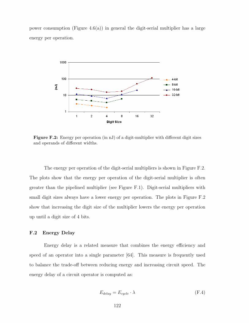
power consumption (Figure 4.6(a)) in general the digit-serial multiplier has a large
energy per operation.
Figure F.2: Energy per operation (in nJ) of a digit-multiplier with different digit sizesand operands of different widths.
The energy per operation of the digit-serial multipliers is shown in Figure F.2.
The plots show that the energy per operation of the digit-serial multiplier is often
greater than the pipelined multiplier (see Figure F.1). Digit-serial multipliers with
small digit sizes always have a lower energy per operation. The plots in Figure F.2
show that increasing the digit size of the multiplier lowers the energy per operation
up until a digit size of 4 bits.
F.2 Energy Delay
Energy delay is a related measure that combines the energy efficiency and
speed of an operator into a single parameter [64]. This measure is frequently used
to balance the trade-off between reducing energy and increasing circuit speed. The
energy delay of a circuit operator is computed as:
Edelay = Ecycle · λ (F.4)
122

where
λ = the latency of a single computation of the operator.
The latency of the operation is λ = tmin·n where n is the number of clock cycles
required to complete a single operation and tmin is the minimum clock time period of
the circuit. Recall that a pipelined multiplier will have n =number of pipeline stages,
and a digit serial multiplier will have n = N/D (where N is the operand widths and
D is the digit size).
The minimum clock time period of a circuit decreases as the amount of pipelin-
ing increases. This smaller clock period provides greater throughput for designs with
single-cycle operations such as the pipelined multipliers. However, as we increase the
amount of pipelining the latency increases (n increases), potentially increasing the
energy delay. Thus, as pipelining is increased the energy delay could increase due to
an increased latency, but the energy delay could also be reduced due the the reduced
amount of glitching.
Figure F.3(a) shows how an increased amount of pipelining could either de-
crease or increase energy delay. In designs which have a large percentage of glitching
(see Figure 4.2) such as the 32-bit multiplier, increasing the amount of pipelining de-
creases the energy delay. In designs with less glitching, energy delay rises as pipelining
is increased.
The trade-off of larger latency for less glitching is accented with the digit-serial
multiplier. The digit-serial multiplier consumes almost no energy due to glitching,
but relative to the pipelined multipliers requires a large number of cycles to complete
an operation. The plots in Figure F.3(b) show the energy density of digit-serial
multipliers. Due to the large amount of glitching in the pipelined array multipliers,
the digit-serial multipliers have a lower energy delay. For the digit-serial multipliers
the energy delay decreases with increasing digit size only up to a certain point (like
energy per operation). The optimal digit size for energy delay appears to be 4 bits.
123

(a) Energy delay (in nJ·ns) for an array multiplier of different widths andvarious amounts of pipelining.
(b) Energy delay (in nJ·ns) of digit-serial multipliers of different digit sizesand operands of different widths.
Figure F.3: The energy delay (in nJ·ns) of different sizes of array and digit-serialmultipliers.
F.3 Energy Throughput
The energy throughput parameter is similar to energy delay in that it combines
energy efficiency and circuit speed into a single parameter. Energy throughput differs
from energy delay in that it does not take into account the number of clock cycles
needed to complete a single operation (n), but rather it considers the number of clock
cycles between successive operation initiations (δ). In most cases only one or the
124

other is used. Energy throughput is calculated as:
Ethput = Ecycle · tmin · δ (F.5)
where
tmin = the minimum clock period of the circuit, and
δ = the data introduction interval.
For pipelined multipliers δ = 1 and for digit-serial multipliers δ = N/D.
Sometimes it is more useful to consider throughput energy rather than energy
delay. In some designs a pipelined operation is used successively in such a way that
a new operation can be initiated on each clock cycle (δ = 1). In these cases, energy
throughput might be a more desirable parameter than energy delay. Energy delay is
more useful for designs which require an operation to complete before a new one can
be initiated (δ = pipedepth).
Where increasing pipeline depth raises energy delay (due to an increased la-
tency), it lowers energy throughput. Pipelining benefits energy throughput in two
ways: it reduces glitches which lowers overall energy consumption, and it reduces
the minimum clock period - providing a greater throughput. Figure F.4(a) shows
how pipelining greatly benefits energy throughput. Energy throughput (in nJ·ns) is
displayed on a logarithmic scale therefore over a range of different pipeline depths
it appears linear. The graph shows how critical the first stages of pipelining are.
Implementing only a single pipeline stage in the 32x32 multiplier reduces the energy
throughput by an order of magnitude.
Energy throughput for the digit-serial multiplier is the same as energy density
since n = δ = N/D (where N is the size of the digit-serial multiplier operands
and D is the digit size). In other words, the data introduction rate is the same as
throughput. Despite its low power consumption (see Figure 4.6(b)) the digit-serial
multiplier tends to have a large energy throughput and energy delay. The digit-serial
125

(a) Energy throughput (in nJ·ns) for an array multiplier of different widthsand various amounts of pipelining.
(b) Energy throughput (in nJ·ns) of digit-serial multipliers of different digitsizes and operands of different widths.
Figure F.4: The energy throughput (in nJ·ns) of different sizes of array and digit-serialmultipliers.
multiplier benefits from having almost no glitching and a smaller clock period than the
pipelined multipliers. However, it suffers from having a large δ value. In almost every
case, this large δ value overshadows the advantages of a low minimum clock period
and minimized glitching. Figure F.4(b) shows the energy throughput for the digit
serial multipliers. As with energy delay, the optimal digit size appears to be 4 bits
(again). Comparing this figure with Figure F.4(a) reveals that as the pipeline depth
of the multipliers increases, they overtake the digit-serial multipliers in efficiency.
126

F.4 Energy Density
The final energy parameter used in this study is energy density, Edensity. This
parameter normalizes the amount of energy required to perform a single operation to
the number of logic resources used by the circuit. This parameter can be calculated
as:
Edensity = Ecycle/A (F.6)
where
A = the “area” of the circuit.
It is important to note that the amount of dynamic energy consumed by a
circuit module is not necessarily linearly related to the size of the circuit. As described
earlier, the primary contributer to dynamic power is signal glitches. Since circuit size
affects energy density, large circuits that reduce glitching through pipelining may have
a lower energy density than smaller pipelined circuits.
Figure F.5(a) shows the energy density for the pipelined multipliers. The
energy trends shown in this figure are the result of glitching and average net activity
rate. As expected, glitching is reduced as pipelining is introduced, lowering the
overall energy consumption. However, the size of the multiplier also affects the energy
density. The nets of a smaller multiplier have a higher average activity rate than a
larger multiplier, thus it is possible for smaller designs with lower energy consumptions
to report a larger energy density. This trend is shown in the digit-serial designs (Figure
F.5(b)).
The graph in Figure F.5(b) shows the energy density of the digit-serial mul-
tipliers. The plots in this figure show that despite being a circuit with a multi-cycle
operation, the digit-serial energy density is almost always lower than the energy den-
sity of the pipelined multipliers. The digit-serial multipliers generally have a smaller
area than the pipelined multipliers. Whereas the area of the pipelined multipliers
has no direct correlation with its energy density, the energy density of the digit-serial
127

(a) Energy density (in pJ/LUT) for an array multiplier of different widthsand various amounts of pipelining.
(b) Energy density (in pJ/LUT) of digit-serial multipliers of different digitsizes and operands of different widths.
Figure F.5: The energy density (in pJ/LUT) of different sizes of array and digit-serialmultipliers.
multipliers is inversely proportional to area. The digit-serial multipliers with 4-bit
operands have the smallest area and the highest energy density. Conversely, the digit-
serial multipliers with 32-bit operands have the largest area and the smallest energy
density.
128

F.5 Clock Energy
Often the additional registers required for pipelining can come at little or no
cost in FPGA designs, since the configurable logic blocks (CLBs) used in the design
have registers included that often go unused. When an ASIC design is pipelined, the
power savings due to glitch reduction has to be weighted against the power increase
due to the increase in register count. Unlike an ASIC design however, in an FPGA
design there is little or no increase in clock power as pipeline depths or digit sizes
are increased. Figures F.6(a) and F.6(b) show the amount of clock energy required
for the pipelined multipliers and digit-serial multipliers respectively. For the digit-
serial multipliers, the clock energy consumed is constant, regardless of the operand
bit width or digit size. The amount of power consumed by the clock is a small fraction
of the total power consumption.
129

(a) Clock energy consumption in pipelined array multipliers
(b) Clock energy consumption in digit-serial multipliers
Figure F.6: Clock energy of different sizes of array and digit-serial multipliers.
130