Embed Size (px)
Citation preview

LM2593HV
Reducing Converter Stresses
Literature Number: SNVA577

Technology Edge
Posted with permission from the May 2002 issue of Power Electronics Technology.®Copyright 2002, PRIMEDIA Business Magazine & Media Inc. All rights reserved
Reducing Converter StressesBy: Sanjaya Maniktala - Principal Engineer
Introduction
When designing or testing DC-DC converters with a wide input voltage range, we are invariably concerned withhow the stresses in the power supply may change with respect to input/line variations. For example, whenconducting stress testing or design validation, one needs to fix an input voltage for the test. But it isn't obviouswhether a given stress is going to be the highest at the maximum or at the minimum of the input voltage range. Orworse, somewhere in the middle of the input voltage range!?
Further, designers used to working with one major topology may be quite surprised when they shift attention toanother topology, because the rules of the game do in fact change suddenly. In fact the answer to what inputvoltage represents the 'worst' condition for a given stress, does have a lot to do with the topology at hand. So forexample, the peak switch current is higher at low input voltages for the Boost and the Buck-Boost, but quite theopposite for the Buck, for which the worst case is at high input voltages. Further, during the design process too,similar puzzling questions can arise. For example, should the inductor be designed at the highest input or thelowest input voltage of the range? For a Buck it didn't seem to matter too much at what input voltage we designthe inductor, but if one applies the same nonchalance to a Boost or a Buck-Boost, there may be no power supplyto put through any further testing.
Among the stresses we have obviously ignored are the voltage stresses, as for them it is clear that the worstcondition is going to be at the maximum input voltage. Besides, designers can easily figure out the requiredvoltage ratings of the devices used, in any given topology. The same applies to load conditions. It is understoodthat maximum load is the worst condition, and that is what we need to design for and test. But the important pointis even while delivering this constant maximum load, the internal currents of the power supply do change theirshape, peak values, RMS and Average values considerably in response to changes in input voltage. The purposeof this article is to figure out how some of these vary and to thereby fix a 'worst case' design or test condition foreach of them.

A comprehensive table of design information (Table 1a in this part and Table 1b in the next part of the article tofollow) is provided for all the three main topologies: the Buck, the Buck-Boost and the Boost. We are considering apower supply of any of these topologies, operating at constant (maximum) load, with a fixed output voltage, whoseinput voltage is varied. We predict the response of a given parameter to the resulting variation in duty cycle, and

thereby figure out the worst case input test or design condition. These conclusions will be summarized in Part 2 ofthis article which follows. The equations are essentially cast in terms of the output voltage (V
O), max load ('I
O') and
Duty Cycle ('D'), and inductor current ripple ratio ('r'). The input voltage 'VIN
' is not included directly in the stress
formulae, as 'D' is intended to reflect the input voltage variation. The most important fact to keep in mind in thisarticle when relating D to V
IN is that for all topologies, low D corresponds to high V
IN and a high D to low V
IN(since output voltage is considered fixed). It will also be noticed that the design table includes the drops across theSwitch ('V
SW') and diode ('V
D') for all the topologies. It was figured that since these 'drops' have become
increasingly important with the present day situation of ever-decreasing input/output voltage rails, it doesn't makesense anymore to approximate them to zero as is often done in related literature. So the table, being a fairlycomplete and accurate reference source of useful design information, was also used to make some importantdesign related conclusions along the way.
In Part 1 of this article we will present the equations for inductor and capacitors. In Part 2 we will take up thesemiconductors, and also plot out the functions referred to in both articles and summarize them in an easy lookuptable.
Inductor Current Waveforms
An inductor current waveform consists of an AC/ramp component 'DI', and a DC/average component 'IDC
', the
latter being the geometric center of the ramp. For the Buck, the average inductor current is the load current, butfor the Boost and the Buck-Boost, the average diode current is the load current. So as from Table 1a, it can beshown that
So it is clear that the average Inductor current becomes very high if D approaches 1 for the Boost and theBuck-Boost. This corresponds to the lowest input voltage 'V
IN_MIN' for these topologies, and the inductor design
must be conducted at this voltage. But for the Buck there is hardly any relationship of inductor design to inputvoltage since the average current depends only on the load (which is considered fixed in our analysis). So for aBuck regulator, as a first pass selection, we often simply pick an inductor with a current rating equal to the load.
The AC component of the inductor current, 'IAC
', or 'DI' cannot be fully ignored even for a Buck. This parameter is
important, firstly, because alongwith IDC
, it determines the peak value of the inductor current. This peak value
needs to be known so as to accurately evaluate the energy handling requirement of the inductor (defined as½*L*I2
PEAK). If we do not size the inductor accordingly, the core may saturate. But more importantly, for all
topologies, this AC component is completely responsible for the core loss (which does not depend on IDC
, so long
as the inductor is not saturating).
Now, for all the topologies, there is an applied voltage 'VON
' applied across the inductor when the switch is ON.
This causes a certain AC ramp component 'DI' across the inductor from the basic equation VON
=L*DI/(D/f) or
DI=VON
*D/(L*f), where f is the frequency. As the input voltage falls, VON also decreases, but D increases. So
what happens to DI?
The term DI is provided in Table 1a. We see that

Plotting these functions out we will see that
where VIN_50
is the input voltage at which D=50% for the topology under consideration. The equation for VIN_50
is
also provided in Table 1a. If the input voltage range does not include VIN_50
, we must choose either VIN_MIN
or
VIN_MAX
, whichever happens to be closer to VIN_50
.
We also define a useful parameter called the current ripple ratio 'r' which is the ratio of the AC to the DC value ofthe inductor current, with the converter delivering maximum load. So
This parameter 'r' is important as it determines among other things, the inductance 'L', and the physical size ofmost of the power components. It can be shown that the size of the inductor is reduced by increasing 'r'. Howeveran 'r' of 0.3-0.4 represents the most optimum choice for any topology. Allowing greater current ripple than thisdoes not appreciably reduce the size of the inductor, but increases the size of the input/output capacitors. Now,having designed the inductor for a given value of 'r' at the appropriate input voltage end, as discussed earlier, aswe vary the input voltage over the expected range, 'r' changes accordingly. The equations in Table 1a are castessentially in terms of 'r' and D, as these are the two main parameters that vary with input voltage. The variation of'r' with D is also provided, thus making D the only actual variable in our analysis . The value of the requiredinductance (based on a chosen 'r') can be found in Table 1a, and the physical size of this inductor can be alsocalculated from the required energy handling capability as listed.
Inductor Energy
The 'Energy Handling Capability' is e=½* L*I2PEAK
. This parameter literally 'sizes' up the inductor for a given
application. Note that the size is not determined just by inductance, since almost any inductance can betheoretically achieved on any core, simply by winding the appropriate number of turns on it. The completeequations for 'e' are provided in Table 1a. For our analysis here, we first make an approximation for the rathercomplicated term involving 'r'. Assuming 'r' to be small this term becomes
From Table 1a, for small 'r', we can see that the Energy handling Capability goes as
Plotting these functions out we will see that

Note that for both the Boost and the Buck-Boost, the required energy handling capability increases dramatically asduty cycle approaches 0.6. This is known to designers of front-end PFC stages. Such stages are typically of Boosttopology, providing an internal 400VDC rail from a worldwide AC input. It is seen that the size of the requiredinductor goes up sharply as the minimum input voltage falls, and so the inductor design should be carried out atthe minimum input voltage. As for the Buck, some designers use the maximum input voltage, some the minimum,and some simply use the nominal input voltage. It really does not matter too much, provided 'r' is, and remains,small as we assumed. In reality, 'r' does increase as input voltage increases (thereby causing a slight increase inpeak value), so it is preferable to design the inductor of a buck regulator for the highest input voltage.
Inductor Avg/RMS Currents
If 'r' is small, the average and RMS values of the inductor current are the same, 'IL'. The copper loss in the
inductor is IL2*R, where 'R' is the winding resistance. The copper loss is usually very large compared to the core
loss (which depends on DI, as discussed earlier), and largely determines the temperature rise of the inductor.
From Table 1a, for small 'r', we can see that the RMS/Avg current goes as
We can see that for the Boost and Buck-Boost, if D is large, IL increases. Therefore when evaluating copper loss
or temperature rise of the inductor for these, we need to use the minimum input voltage. For the Buck, since 'r'does increase with increasing input voltage, the RMS value of the inductor current is also higher, and so weshould use the maximum input voltage.
Input Capacitor Currents
A key parameter is the RMS current ,'IIN
', through the input electrolytic capacitor. It determines the basic/minimum
selection criterion since the capacitor must be rated at least for the worst case RMS current that may pass throughit. A capacitor operated with an RMS current higher than its rated value, is not guaranteed to have any specific lifeby most manufacturers. Life expectancy vs. temperature curves/equations as provided, are then not considered tobe valid.
From Table 1a, for small 'r', we can see that this goes as
Plotting these functions out we will see that

So the temperature of the output capacitor must also be evaluated at the above input voltages. If the input voltagerange does not include V
IN_50, we must choose either V
IN_MIN or V
IN_MAX, whichever happens to be closer to
VIN_50
.
We are also concerned with the peak to peak current, IPP_IN
through the input capacitor as this determines the
input voltage ripple DVIN
=IPP_IN
*ESRIN
, where ESRIN
is the Equivalent Series Resistance of the input capacitor.
This input ripple is a major component of the EMI spectrum at the input of the power supply.
From Table 1a, for small 'r', we can see that this goes as
Plotting these functions out we will see that
For a Buck stage, the input voltage ripple is almost a constant with respect to input voltage variations, provided 'r'is very small. However since 'r' does increase somewhat at high input voltages, it is preferable to evaluate thisparameter at the highest input voltage.
Output Capacitor Currents
The Output Capacitor also needs to be at least big enough to handle the worst case RMS current through it, 'IOUT
'.
From Table 1a, for small 'r', we can see that this goes as
Plotting these functions out we will see that
So the temperature of the output capacitor must also be evaluated at the above input voltages.
We are also concerned with the peak to peak current, IPP_OUT
through the output capacitor as this determines the

output voltage ripple DVOUT
=IPP_OUT
*ESROUT
, where ESROUT
is the Equivalent Series Resistance of the output
capacitor. This output ripple is a major component of the noise spectrum at the output of the power supply.
From Table 1a, for small 'r', we can see that this goes as
Plotting these functions out we will see that
Switch RMS/Avg Current
For a MOSFET Switch we need to calculate the conduction loss as given by I2RMS
*rds. The crossover losses are
lowest at the minimum input voltage. But since they are usually a small fraction of the conduction losses, and arethus ignored here. The I
RMS of the switch varies in the following manner
From Table 1b, for small 'r', we can see that this goes as

Plotting these functions out we will see that
It should however be noted that for a Buck, the dissipation in the Switch at low input voltages goes up only slightly,but for the remaining topologies, this dissipation is expected to go up steeply at low input voltages, leading to alarge drop in efficiency. In Table 1b, the average switch current is also provided, for calculation of dissipation inbipolar switches. It can be shown that the above conclusions for RMS are also valid for the average value of theswitch current (which is required to calculate the conduction loss for a bipolar switch).
Talking about efficiency leads to the other main component of loss in a power supply, the diode loss. We will nowsee how this varies, and what it implies for the effect of input variations on the efficiency of the power supply.
Average Diode Current/Efficiency
For a diode we need to calculate the forward loss as given by IAVG
*VD, where 'V
D' is the drop across the diode
when it conducts. For the Boost and the Buck-Boost, the average diode current is the load current, so it is notgoing to change with duty cycle. But for the Buck it does vary.
From Table 1b, we can see that this goes as
Plotting these out in Figure 1, we can see that
We saw that the dissipation in the switch of a Buck remains almost constant as input voltage increases, but nowwe see that the diode dissipation increases as we do so. So we expect the efficiency of a Buck regulator to fall athigh input voltages on account of increased diode dissipation (assuming the drop across switch is less than thedrop across the diode). For the Boost and Buck-Boost, the diode dissipation does not change as input voltagefalls, but the switch dissipation increases dramatically. So we expect the efficiency of a Boost or a Buck-Boost tofall at low input voltages on account of increased switch dissipation (unless crossover losses are very large, inwhich case the reverse is occasionally found to be true).

For diode temperatures, we need to test a Buck regulator at the highest input voltage. For the other topologies, itdoes not matter. This is shown as 'V
IN' in Table 2, implying any input voltage.

Peak Switch Current
This parameter is important because every controller has a current limit for the switch, and if the calculated peakexceeds the lowest value possible of the switch current limit, anywhere in the input voltage range, the requiredoutput power cannot be delivered. The peak current in a Buck is just a little higher than the load current, and so forexample, the LM2593HV 'Step Down (Buck) regulator' IC from National Semiconductor, which is designed for '2Aload', has a minimum set value of 2.3A for the switch current limit. Yet, as seen in Figure 2, and from thedatasheet of this device, this Buck IC can be operated as a 'positive to negative' regulator, which is actually astandard Buck-Boost topology. In this mode, the peak current values are much higher, as can be seen from Table1b, and in fact depend not only on load, but on the duty cycle/input voltage too. We now try to see how the peakcurrent values vary for all the topologies, with changes in input voltage.
From Table 1b, for small 'r', we can see that the peak current goes as
Plotting these functions we will see that for the Boost and the Buck-Boost the peak value of switch current occursat maximum duty cycle (minimum input voltage), whereas for the Buck this occurs at lowest duty cycle (highestinput voltage). Therefore Current Limit must be tested at minimum input voltage for the Boost and the Buck-Boost,but for the Buck we must go to the highest input voltage. We conclude
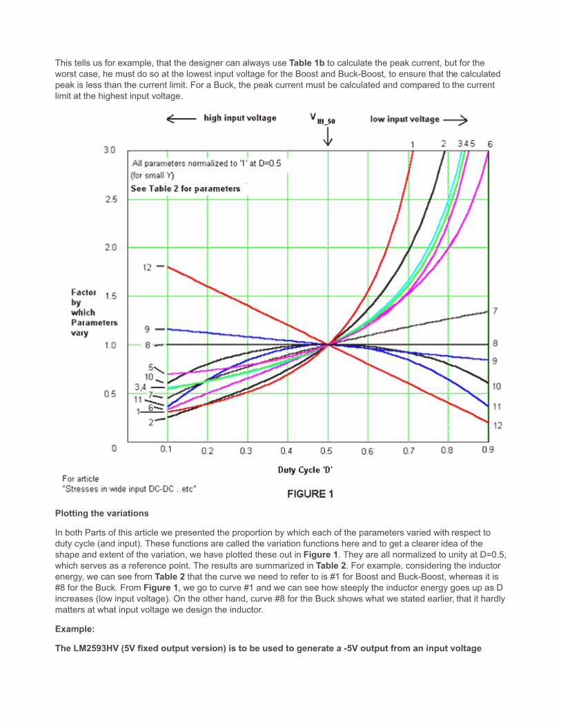
This tells us for example, that the designer can always use Table 1b to calculate the peak current, but for theworst case, he must do so at the lowest input voltage for the Boost and Buck-Boost, to ensure that the calculatedpeak is less than the current limit. For a Buck, the peak current must be calculated and compared to the currentlimit at the highest input voltage.
Plotting the variations
In both Parts of this article we presented the proportion by which each of the parameters varied with respect toduty cycle (and input). These functions are called the variation functions here and to get a clearer idea of theshape and extent of the variation, we have plotted these out in Figure 1. They are all normalized to unity at D=0.5,which serves as a reference point. The results are summarized in Table 2. For example, considering the inductorenergy, we can see from Table 2 that the curve we need to refer to is #1 for Boost and Buck-Boost, whereas it is#8 for the Buck. From Figure 1, we go to curve #1 and we can see how steeply the inductor energy goes up as Dincreases (low input voltage). On the other hand, curve #8 for the Buck shows what we stated earlier, that it hardlymatters at what input voltage we design the inductor.
Example:
The LM2593HV (5V fixed output version) is to be used to generate a -5V output from an input voltage
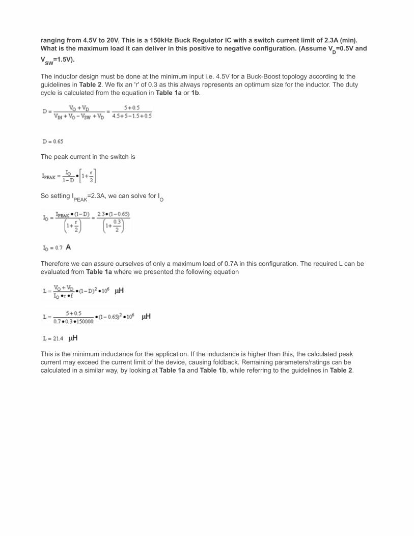
ranging from 4.5V to 20V. This is a 150kHz Buck Regulator IC with a switch current limit of 2.3A (min).What is the maximum load it can deliver in this positive to negative configuration. (Assume VD=0.5V andVSW=1.5V).
The inductor design must be done at the minimum input i.e. 4.5V for a Buck-Boost topology according to theguidelines in Table 2. We fix an 'r' of 0.3 as this always represents an optimum size for the inductor. The dutycycle is calculated from the equation in Table 1a or 1b.
The peak current in the switch is
So setting IPEAK
=2.3A, we can solve for IO
Therefore we can assure ourselves of only a maximum load of 0.7A in this configuration. The required L can beevaluated from Table 1a where we presented the following equation
This is the minimum inductance for the application. If the inductance is higher than this, the calculated peakcurrent may exceed the current limit of the device, causing foldback. Remaining parameters/ratings can becalculated in a similar way, by looking at Table 1a and Table 1b, while referring to the guidelines in Table 2.

IMPORTANT NOTICE
Texas Instruments Incorporated and its subsidiaries (TI) reserve the right to make corrections, modifications, enhancements, improvements,and other changes to its products and services at any time and to discontinue any product or service without notice. Customers shouldobtain the latest relevant information before placing orders and should verify that such information is current and complete. All products aresold subject to TI’s terms and conditions of sale supplied at the time of order acknowledgment.
TI warrants performance of its hardware products to the specifications applicable at the time of sale in accordance with TI’s standardwarranty. Testing and other quality control techniques are used to the extent TI deems necessary to support this warranty. Except wheremandated by government requirements, testing of all parameters of each product is not necessarily performed.
TI assumes no liability for applications assistance or customer product design. Customers are responsible for their products andapplications using TI components. To minimize the risks associated with customer products and applications, customers should provideadequate design and operating safeguards.
TI does not warrant or represent that any license, either express or implied, is granted under any TI patent right, copyright, mask work right,or other TI intellectual property right relating to any combination, machine, or process in which TI products or services are used. Informationpublished by TI regarding third-party products or services does not constitute a license from TI to use such products or services or awarranty or endorsement thereof. Use of such information may require a license from a third party under the patents or other intellectualproperty of the third party, or a license from TI under the patents or other intellectual property of TI.
Reproduction of TI information in TI data books or data sheets is permissible only if reproduction is without alteration and is accompaniedby all associated warranties, conditions, limitations, and notices. Reproduction of this information with alteration is an unfair and deceptivebusiness practice. TI is not responsible or liable for such altered documentation. Information of third parties may be subject to additionalrestrictions.
Resale of TI products or services with statements different from or beyond the parameters stated by TI for that product or service voids allexpress and any implied warranties for the associated TI product or service and is an unfair and deceptive business practice. TI is notresponsible or liable for any such statements.
TI products are not authorized for use in safety-critical applications (such as life support) where a failure of the TI product would reasonablybe expected to cause severe personal injury or death, unless officers of the parties have executed an agreement specifically governingsuch use. Buyers represent that they have all necessary expertise in the safety and regulatory ramifications of their applications, andacknowledge and agree that they are solely responsible for all legal, regulatory and safety-related requirements concerning their productsand any use of TI products in such safety-critical applications, notwithstanding any applications-related information or support that may beprovided by TI. Further, Buyers must fully indemnify TI and its representatives against any damages arising out of the use of TI products insuch safety-critical applications.
TI products are neither designed nor intended for use in military/aerospace applications or environments unless the TI products arespecifically designated by TI as military-grade or "enhanced plastic." Only products designated by TI as military-grade meet militaryspecifications. Buyers acknowledge and agree that any such use of TI products which TI has not designated as military-grade is solely atthe Buyer's risk, and that they are solely responsible for compliance with all legal and regulatory requirements in connection with such use.
TI products are neither designed nor intended for use in automotive applications or environments unless the specific TI products aredesignated by TI as compliant with ISO/TS 16949 requirements. Buyers acknowledge and agree that, if they use any non-designatedproducts in automotive applications, TI will not be responsible for any failure to meet such requirements.
Following are URLs where you can obtain information on other Texas Instruments products and application solutions:
Products Applications
Audio www.ti.com/audio Communications and Telecom www.ti.com/communications
Amplifiers amplifier.ti.com Computers and Peripherals www.ti.com/computers
Data Converters dataconverter.ti.com Consumer Electronics www.ti.com/consumer-apps
DLP® Products www.dlp.com Energy and Lighting www.ti.com/energy
DSP dsp.ti.com Industrial www.ti.com/industrial
Clocks and Timers www.ti.com/clocks Medical www.ti.com/medical
Interface interface.ti.com Security www.ti.com/security
Logic logic.ti.com Space, Avionics and Defense www.ti.com/space-avionics-defense
Power Mgmt power.ti.com Transportation and Automotive www.ti.com/automotive
Microcontrollers microcontroller.ti.com Video and Imaging www.ti.com/video
RFID www.ti-rfid.com
OMAP Mobile Processors www.ti.com/omap
Wireless Connectivity www.ti.com/wirelessconnectivity
TI E2E Community Home Page e2e.ti.com
Mailing Address: Texas Instruments, Post Office Box 655303, Dallas, Texas 75265Copyright © 2011, Texas Instruments Incorporated