Embed Size (px)
Citation preview
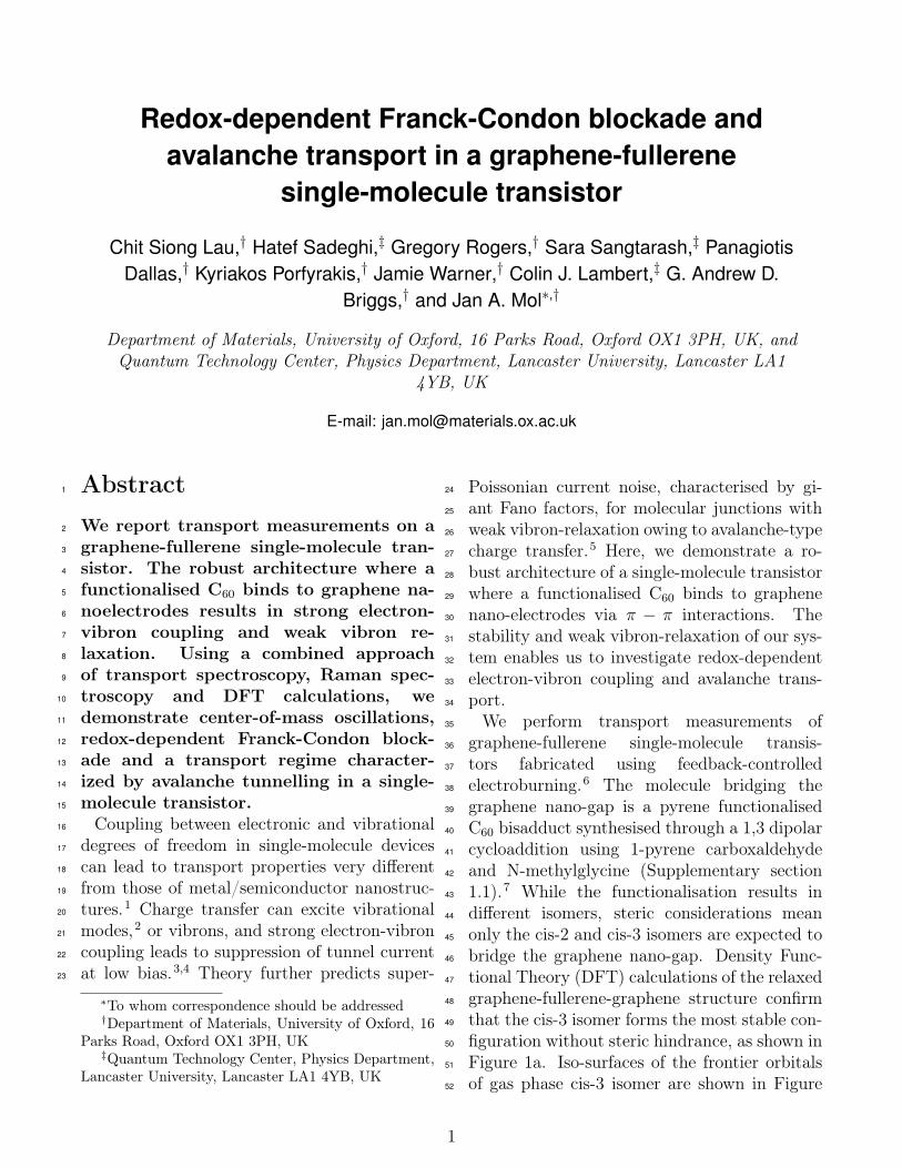
Redox-dependent Franck-Condon blockade andavalanche transport in a graphene-fullerene
single-molecule transistor
Chit Siong Lau,† Hatef Sadeghi,‡ Gregory Rogers,† Sara Sangtarash,‡ PanagiotisDallas,† Kyriakos Porfyrakis,† Jamie Warner,† Colin J. Lambert,‡ G. Andrew D.
Briggs,† and Jan A. Mol∗,†
Department of Materials, University of Oxford, 16 Parks Road, Oxford OX1 3PH, UK, andQuantum Technology Center, Physics Department, Lancaster University, Lancaster LA1
4YB, UK
E-mail: [email protected]
Abstract1
We report transport measurements on a2
graphene-fullerene single-molecule tran-3
sistor. The robust architecture where a4
functionalised C60 binds to graphene na-5
noelectrodes results in strong electron-6
vibron coupling and weak vibron re-7
laxation. Using a combined approach8
of transport spectroscopy, Raman spec-9
troscopy and DFT calculations, we10
demonstrate center-of-mass oscillations,11
redox-dependent Franck-Condon block-12
ade and a transport regime character-13
ized by avalanche tunnelling in a single-14
molecule transistor.15
Coupling between electronic and vibrational16
degrees of freedom in single-molecule devices17
can lead to transport properties very different18
from those of metal/semiconductor nanostruc-19
tures.1 Charge transfer can excite vibrational20
modes,2 or vibrons, and strong electron-vibron21
coupling leads to suppression of tunnel current22
at low bias.3,4 Theory further predicts super-23
∗To whom correspondence should be addressed†Department of Materials, University of Oxford, 16
Parks Road, Oxford OX1 3PH, UK‡Quantum Technology Center, Physics Department,
Lancaster University, Lancaster LA1 4YB, UK
Poissonian current noise, characterised by gi-24
ant Fano factors, for molecular junctions with25
weak vibron-relaxation owing to avalanche-type26
charge transfer.5 Here, we demonstrate a ro-27
bust architecture of a single-molecule transistor28
where a functionalised C60 binds to graphene29
nano-electrodes via π − π interactions. The30
stability and weak vibron-relaxation of our sys-31
tem enables us to investigate redox-dependent32
electron-vibron coupling and avalanche trans-33
port.34
We perform transport measurements of35
graphene-fullerene single-molecule transis-36
tors fabricated using feedback-controlled37
electroburning.6 The molecule bridging the38
graphene nano-gap is a pyrene functionalised39
C60 bisadduct synthesised through a 1,3 dipolar40
cycloaddition using 1-pyrene carboxaldehyde41
and N-methylglycine (Supplementary section42
1.1).7 While the functionalisation results in43
different isomers, steric considerations mean44
only the cis-2 and cis-3 isomers are expected to45
bridge the graphene nano-gap. Density Func-46
tional Theory (DFT) calculations of the relaxed47
graphene-fullerene-graphene structure confirm48
that the cis-3 isomer forms the most stable con-49
figuration without steric hindrance, as shown in50
Figure 1a. Iso-surfaces of the frontier orbitals51
of gas phase cis-3 isomer are shown in Figure52
1
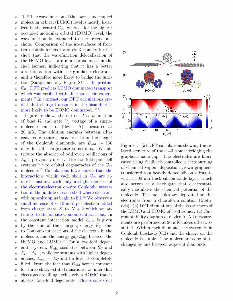
1b.8 The wavefunction of the lowest unoccupied53
molecular orbital (LUMO) level is mostly local-54
ized in the central C60, whereas for the highest55
occupied molecular orbital (HOMO) level, the56
wavefunction is extended to the pyrene an-57
chors. Comparison of the iso-surfaces of fron-58
tier orbitals for cis-2 and cis-3 isomers further59
show that the wavefunction delocalization of60
the HOMO levels are more pronounced in the61
cis-3 isomer, indicating that it has a better62
π-π interaction with the graphene electrodes63
and is therefore more likely to bridge the junc-64
tion (Supplementary Figure S11). In pristine65
C60, DFT predicts LUMO dominated transport66
which was verified with thermoelectric experi-67
ments.9 In contrast, our DFT calculations pre-68
dict that charge transport in the bisadduct is69
more likely to be HOMO dominated.10,1170
Figure 1c shows the current I as a function71
of bias Vb and gate Vg voltage of a single-72
molecule transistor (device A), measured at73
20 mK. The addition energies between adja-74
cent redox states, measured from the height75
of the Coulomb diamonds, are Eadd ∼ 16076
meV for all charge-state transitions. We at-77
tribute the absence of odd/even oscillations of78
Eadd, previously observed for two-fold spin shell79
systems,6,12 to orbital degeneracies of the C6080
molecule.13 Calculations have shown that the81
interactions within each shell in C60 are al-82
most constant, with only a slight increase of83
the electron-electron on-site Coulomb interac-84
tion in the middle of each shell where electrons85
with opposite spins begin to fill.13 We observe a86
small increase of ∼ 10 meV per electron added87
from charge state N to N + 2 which we at-88
tribute to the on-site Coulomb interactions. In89
the constant interaction model Eadd is given90
by the sum of the charging energy EC , due91
to Coulomb interactions of the electrons in the92
molecule, and the energy gap ∆HL between the93
HOMO and LUMO.14 For a two-fold degen-94
erate system, Eadd oscillates between EC and95
EC +∆HL, while for systems with higher degen-96
eracies, Eadd = EC until a level is completely97
filled. From the fact that Eadd here is constant98
for three charge-state transitions, we infer that99
electrons are filling exclusively a HOMO that is100
at least four-fold degenerate. This is consistent101
Figure 1: (a) DFT calculations showing the re-laxed structure of the cis-3 isomer bridging thegraphene nano-gap. The electrodes are fabri-cated using feedback-controlled electroburningof chemical vapour deposition grown graphenetransferred to a heavily doped silicon substratewith a 300 nm thick silicon oxide layer, whichalso serves as a back-gate that electrostati-cally modulates the chemical potential of themolecule. The molecules are deposited on theelectrodes from a chloroform solution (Meth-ods). (b) DFT simulations of the iso-surfaces ofthe LUMO and HOMO of cis-3 isomer. (c) Cur-rent stability diagram of device A. All measure-ments are performed at 20 mK unless otherwisestated. Within each diamond, the system is inCoulomb blockade (CB) and the charge on themolecule is stable. The molecular redox statechanges by one between adjacent diamonds.
2
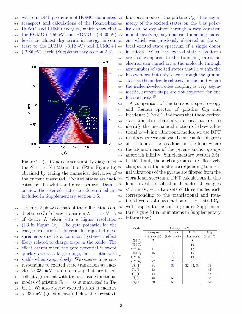
with our DFT prediction of HOMO dominated102
transport and calculations of the Kohn-Sham103
HOMO and LUMO energies, which show that104
the HOMO (-4.59 eV) and HOMO-1 (-4.60 eV)105
levels are almost degenerate in energy, in con-106
trast to the LUMO (-3.12 eV) and LUMO+1107
(-2.86 eV) levels (Supplementary section 2.3).108
Figure 2: (a) Conductance stability diagram ofthe N + 1 to N + 2 transition (P3 in Figure 1c)obtained by taking the numerical derivative ofthe current measured. Excited states are indi-cated by the white and green arrows. Detailson how the excited states are determined areincluded in Supplementary section 1.5.
Figure 2 shows a map of the differential con-109
ductance G of charge transition N + 1 to N + 2110
of device A taken with a higher resolution111
(P3 in Figure 1c). The gate potential for the112
charge transition is different for repeated mea-113
surements due to a common hysteretic effect114
likely related to charge traps in the oxide. The115
effect occurs when the gate potential is swept116
quickly across a large range, but is otherwise117
stable when swept slowly. We observe lines cor-118
responding to excited state transitions at ener-119
gies ≥ 33 meV (white arrows) that are in ex-120
cellent agreement with the intrinsic vibrational121
modes of pristine C60,15 as summarized in Ta-122
ble 1. We also observe excited states at energies123
< 33 meV (green arrows), below the lowest vi-124
brational mode of the pristine C60. The asym-125
metry of the excited states on the bias polar-126
ity can be explained through a rate equation127
model involving asymmetric tunnelling barri-128
ers, which was previously observed in the or-129
bital excited state spectrum of a single donor130
in silicon. When the excited state relaxations131
are fast compared to the tunneling rates, an132
electron can tunnel on to the molecule through133
any number of excited states that lie within the134
bias window but only leave through the ground135
state as the molecule relaxes. In the limit where136
the molecule-electrodes coupling is very asym-137
metric, current steps are not expected for one138
bias polarity.16139
A comparison of the transport spectroscopy140
and Raman spectra of pristine C60 and141
bisadduct (Table 1) indicates that these excited142
state transitions have a vibrational nature. To143
identify the mechanical motion of these addi-144
tional low-lying vibrational modes, we use DFT145
results where we analyse the mechanical degrees146
of freedom of the bisadduct in the limit where147
the atomic mass of the pyrene anchor groups148
approach infinity (Supplementary section 2.6).149
In this limit, the anchor groups are effectively150
clamped and the modes corresponding to inter-151
nal vibrations of the pyrene are filtered from the152
vibrational spectrum. DFT calculations in this153
limit reveal six vibrational modes at energies154
< 33 meV, with two sets of three modes each155
corresponding to the translational and rota-156
tional center-of-mass motion of the central C60157
with respect to the anchor groups (Supplemen-158
tary Figure S13a, animations in Supplementary159
Information).160
Mode Energy (meV)Transport Raman DFT C60
(this work) (this work) (this work) (Ref.15)CM Ty 7 8CM Tx 10CM Rz 11 13 12CM Tz 16 16 16CM Rx 21 19 19CM Ry 27 25 21Hg(1) 34 33 32, 33, 34 33T2u(1) 42 43Gu(1) 42 43Hg(2) 48 55 53Ag(1) 60 61 61
161
3
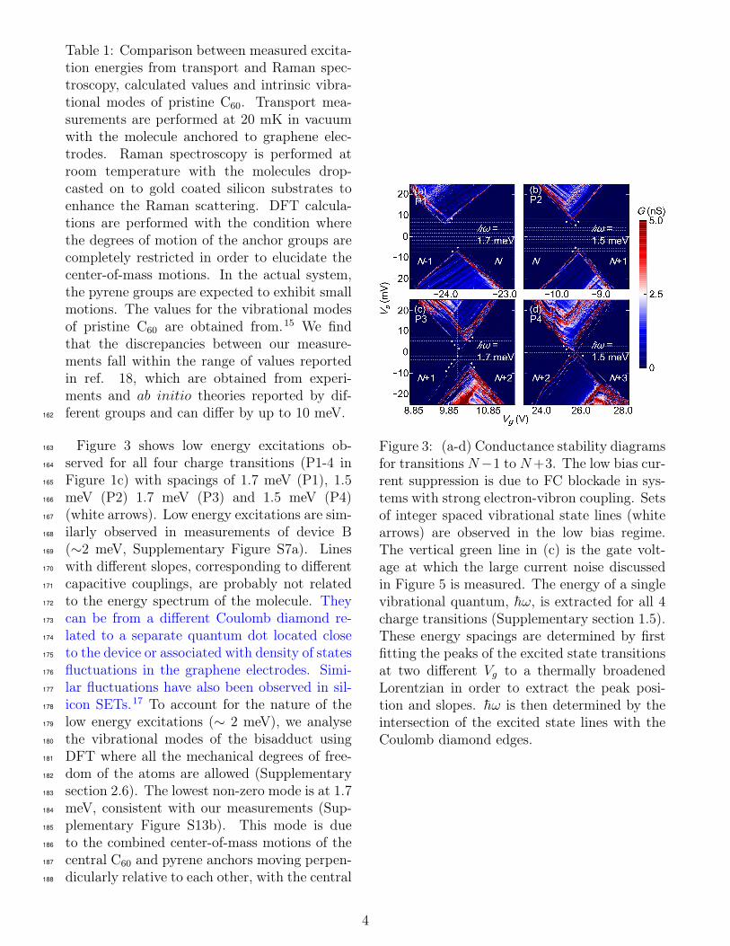
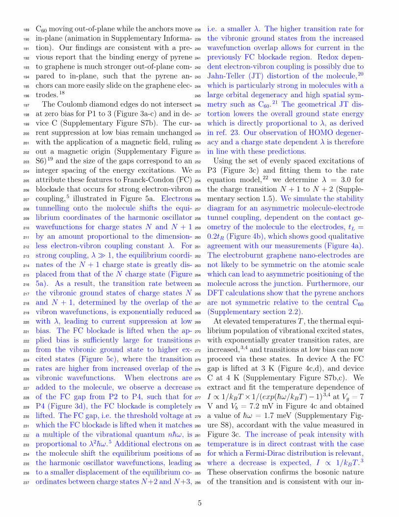
Table 1: Comparison between measured excita-tion energies from transport and Raman spec-troscopy, calculated values and intrinsic vibra-tional modes of pristine C60. Transport mea-surements are performed at 20 mK in vacuumwith the molecule anchored to graphene elec-trodes. Raman spectroscopy is performed atroom temperature with the molecules drop-casted on to gold coated silicon substrates toenhance the Raman scattering. DFT calcula-tions are performed with the condition wherethe degrees of motion of the anchor groups arecompletely restricted in order to elucidate thecenter-of-mass motions. In the actual system,the pyrene groups are expected to exhibit smallmotions. The values for the vibrational modesof pristine C60 are obtained from.15 We findthat the discrepancies between our measure-ments fall within the range of values reportedin ref. 18, which are obtained from experi-ments and ab initio theories reported by dif-ferent groups and can differ by up to 10 meV.162
Figure 3 shows low energy excitations ob-163
served for all four charge transitions (P1-4 in164
Figure 1c) with spacings of 1.7 meV (P1), 1.5165
meV (P2) 1.7 meV (P3) and 1.5 meV (P4)166
(white arrows). Low energy excitations are sim-167
ilarly observed in measurements of device B168
(∼2 meV, Supplementary Figure S7a). Lines169
with different slopes, corresponding to different170
capacitive couplings, are probably not related171
to the energy spectrum of the molecule. They172
can be from a different Coulomb diamond re-173
lated to a separate quantum dot located close174
to the device or associated with density of states175
fluctuations in the graphene electrodes. Simi-176
lar fluctuations have also been observed in sil-177
icon SETs.17 To account for the nature of the178
low energy excitations (∼ 2 meV), we analyse179
the vibrational modes of the bisadduct using180
DFT where all the mechanical degrees of free-181
dom of the atoms are allowed (Supplementary182
section 2.6). The lowest non-zero mode is at 1.7183
meV, consistent with our measurements (Sup-184
plementary Figure S13b). This mode is due185
to the combined center-of-mass motions of the186
central C60 and pyrene anchors moving perpen-187
dicularly relative to each other, with the central188
Figure 3: (a-d) Conductance stability diagramsfor transitions N−1 to N+3. The low bias cur-rent suppression is due to FC blockade in sys-tems with strong electron-vibron coupling. Setsof integer spaced vibrational state lines (whitearrows) are observed in the low bias regime.The vertical green line in (c) is the gate volt-age at which the large current noise discussedin Figure 5 is measured. The energy of a singlevibrational quantum, h̄ω, is extracted for all 4charge transitions (Supplementary section 1.5).These energy spacings are determined by firstfitting the peaks of the excited state transitionsat two different Vg to a thermally broadenedLorentzian in order to extract the peak posi-tion and slopes. h̄ω is then determined by theintersection of the excited state lines with theCoulomb diamond edges.
4
C60 moving out-of-plane while the anchors move189
in-plane (animation in Supplementary Informa-190
tion). Our findings are consistent with a pre-191
vious report that the binding energy of pyrene192
to graphene is much stronger out-of-plane com-193
pared to in-plane, such that the pyrene an-194
chors can more easily slide on the graphene elec-195
trodes.18196
The Coulomb diamond edges do not intersect197
at zero bias for P1 to 3 (Figure 3a-c) and in de-198
vice C (Supplementary Figure S7b). The cur-199
rent suppression at low bias remain unchanged200
with the application of a magnetic field, ruling201
out a magnetic origin (Supplementary Figure202
S6)19 and the size of the gaps correspond to an203
integer spacing of the energy excitations. We204
attribute these features to Franck-Condon (FC)205
blockade that occurs for strong electron-vibron206
coupling,5 illustrated in Figure 5a. Electrons207
tunnelling onto the molecule shifts the equi-208
librium coordinates of the harmonic oscillator209
wavefunctions for charge states N and N + 1210
by an amount proportional to the dimension-211
less electron-vibron coupling constant λ. For212
strong coupling, λ� 1, the equilibrium coordi-213
nates of the N + 1 charge state is greatly dis-214
placed from that of the N charge state (Figure215
5a). As a result, the transition rate between216
the vibronic ground states of charge states N217
and N + 1, determined by the overlap of the218
vibron wavefunctions, is exponentially reduced219
with λ, leading to current suppression at low220
bias. The FC blockade is lifted when the ap-221
plied bias is sufficiently large for transitions222
from the vibronic ground state to higher ex-223
cited states (Figure 5c), where the transition224
rates are higher from increased overlap of the225
vibronic wavefunctions. When electrons are226
added to the molecule, we observe a decrease227
of the FC gap from P2 to P4, such that for228
P4 (Figure 3d), the FC blockade is completely229
lifted. The FC gap, i.e. the threshold voltage at230
which the FC blockade is lifted when it matches231
a multiple of the vibrational quantum nh̄ω, is232
proportional to λ2h̄ω.5 Additional electrons on233
the molecule shift the equilibrium positions of234
the harmonic oscillator wavefunctions, leading235
to a smaller displacement of the equilibrium co-236
ordinates between charge statesN+2 andN+3,237
i.e. a smaller λ. The higher transition rate for238
the vibronic ground states from the increased239
wavefunction overlap allows for current in the240
previously FC blockade region. Redox depen-241
dent electron-vibron coupling is possibly due to242
Jahn-Teller (JT) distortion of the molecule,20243
which is particularly strong in molecules with a244
large orbital degeneracy and high spatial sym-245
metry such as C60.21 The geometrical JT dis-246
tortion lowers the overall ground state energy247
which is directly proportional to λ, as derived248
in ref. 23. Our observation of HOMO degener-249
acy and a charge state dependent λ is therefore250
in line with these predictions.251
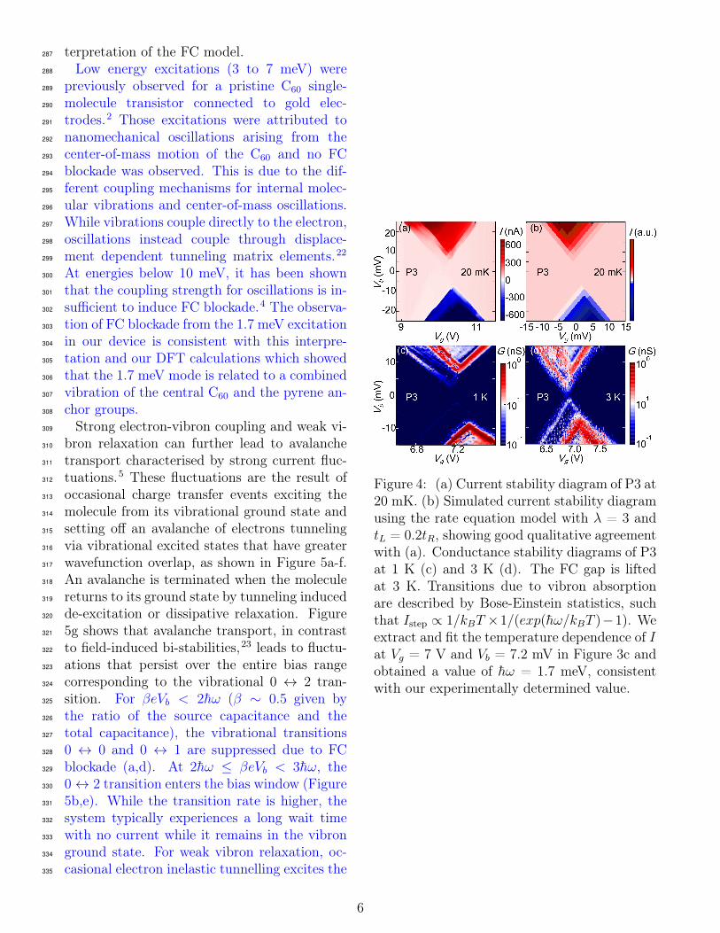
Using the set of evenly spaced excitations of252
P3 (Figure 3c) and fitting them to the rate253
equation model,22 we determine λ = 3.0 for254
the charge transition N + 1 to N + 2 (Supple-255
mentary section 1.5). We simulate the stability256
diagram for an asymmetric molecule-electrode257
tunnel coupling, dependent on the contact ge-258
ometry of the molecule to the electrodes, tL =259
0.2tR (Figure 4b), which shows good qualitative260
agreement with our measurements (Figure 4a).261
The electroburnt graphene nano-electrodes are262
not likely to be symmetric on the atomic scale263
which can lead to asymmetric positioning of the264
molecule across the junction. Furthermore, our265
DFT calculations show that the pyrene anchors266
are not symmetric relative to the central C60267
(Supplementary section 2.2).268
At elevated temperatures T , the thermal equi-269
librium population of vibrational excited states,270
with exponentially greater transition rates, are271
increased,3,4 and transitions at low bias can now272
proceed via these states. In device A the FC273
gap is lifted at 3 K (Figure 4c,d), and device274
C at 4 K (Supplementary Figure S7b,c). We275
extract and fit the temperature dependence of276
I ∝ 1/kBT ×1/(exp(h̄ω/kBT )−1)3,4 at Vg = 7277
V and Vb = 7.2 mV in Figure 4c and obtained278
a value of h̄ω = 1.7 meV (Supplementary Fig-279
ure S8), accordant with the value measured in280
Figure 3c. The increase of peak intensity with281
temperature is in direct contrast with the case282
for which a Fermi-Dirac distribution is relevant,283
where a decrease is expected, I ∝ 1/kBT .3284
These observation confirms the bosonic nature285
of the transition and is consistent with our in-286
5
terpretation of the FC model.287
Low energy excitations (3 to 7 meV) were288
previously observed for a pristine C60 single-289
molecule transistor connected to gold elec-290
trodes.2 Those excitations were attributed to291
nanomechanical oscillations arising from the292
center-of-mass motion of the C60 and no FC293
blockade was observed. This is due to the dif-294
ferent coupling mechanisms for internal molec-295
ular vibrations and center-of-mass oscillations.296
While vibrations couple directly to the electron,297
oscillations instead couple through displace-298
ment dependent tunneling matrix elements.22299
At energies below 10 meV, it has been shown300
that the coupling strength for oscillations is in-301
sufficient to induce FC blockade.4 The observa-302
tion of FC blockade from the 1.7 meV excitation303
in our device is consistent with this interpre-304
tation and our DFT calculations which showed305
that the 1.7 meV mode is related to a combined306
vibration of the central C60 and the pyrene an-307
chor groups.308
Strong electron-vibron coupling and weak vi-309
bron relaxation can further lead to avalanche310
transport characterised by strong current fluc-311
tuations.5 These fluctuations are the result of312
occasional charge transfer events exciting the313
molecule from its vibrational ground state and314
setting off an avalanche of electrons tunneling315
via vibrational excited states that have greater316
wavefunction overlap, as shown in Figure 5a-f.317
An avalanche is terminated when the molecule318
returns to its ground state by tunneling induced319
de-excitation or dissipative relaxation. Figure320
5g shows that avalanche transport, in contrast321
to field-induced bi-stabilities,23 leads to fluctu-322
ations that persist over the entire bias range323
corresponding to the vibrational 0 ↔ 2 tran-324
sition. For βeVb < 2h̄ω (β ∼ 0.5 given by325
the ratio of the source capacitance and the326
total capacitance), the vibrational transitions327
0 ↔ 0 and 0 ↔ 1 are suppressed due to FC328
blockade (a,d). At 2h̄ω ≤ βeVb < 3h̄ω, the329
0↔ 2 transition enters the bias window (Figure330
5b,e). While the transition rate is higher, the331
system typically experiences a long wait time332
with no current while it remains in the vibron333
ground state. For weak vibron relaxation, oc-334
casional electron inelastic tunnelling excites the335
Figure 4: (a) Current stability diagram of P3 at20 mK. (b) Simulated current stability diagramusing the rate equation model with λ = 3 andtL = 0.2tR, showing good qualitative agreementwith (a). Conductance stability diagrams of P3at 1 K (c) and 3 K (d). The FC gap is liftedat 3 K. Transitions due to vibron absorptionare described by Bose-Einstein statistics, suchthat Istep ∝ 1/kBT ×1/(exp(h̄ω/kBT )−1). Weextract and fit the temperature dependence of Iat Vg = 7 V and Vb = 7.2 mV in Figure 3c andobtained a value of h̄ω = 1.7 meV, consistentwith our experimentally determined value.
6
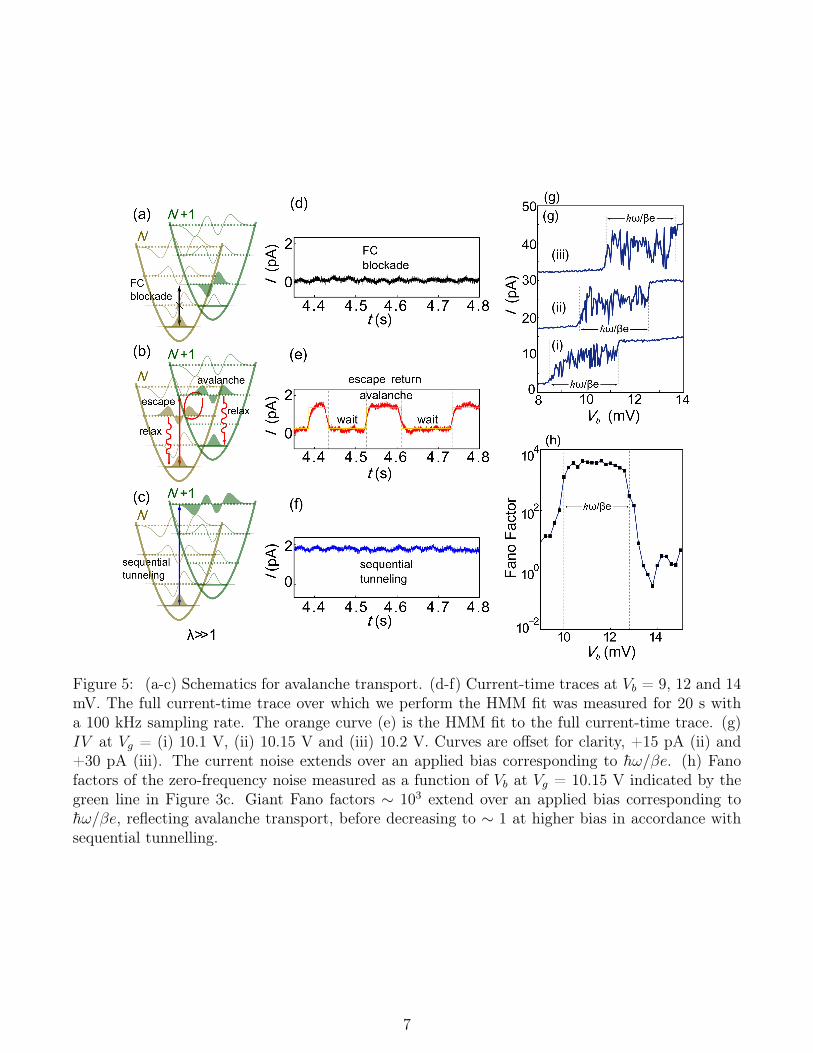
Figure 5: (a-c) Schematics for avalanche transport. (d-f) Current-time traces at Vb = 9, 12 and 14mV. The full current-time trace over which we perform the HMM fit was measured for 20 s witha 100 kHz sampling rate. The orange curve (e) is the HMM fit to the full current-time trace. (g)IV at Vg = (i) 10.1 V, (ii) 10.15 V and (iii) 10.2 V. Curves are offset for clarity, +15 pA (ii) and+30 pA (iii). The current noise extends over an applied bias corresponding to h̄ω/βe. (h) Fanofactors of the zero-frequency noise measured as a function of Vb at Vg = 10.15 V indicated by thegreen line in Figure 3c. Giant Fano factors ∼ 103 extend over an applied bias corresponding toh̄ω/βe, reflecting avalanche transport, before decreasing to ∼ 1 at higher bias in accordance withsequential tunnelling.
7
molecule to a higher vibrational state, with sub-336
sequent tunnelling events further increasing this337
excitation. Having escaped the ground state,338
an avalanche of tunnelling events occur. The339
process terminates when the system returns to340
the vibrational ground state, resulting in an-341
other long wait time before the cycle repeats.342
At βeVb ≥ 3h̄ω, charge transfer proceeds via343
sequential tunnelling through the 0↔ 3 transi-344
tion (Figure 5c,f).345
To characterise the current fluctuations we346
extract the 0 ↔ 2 escape and return rates by347
fitting a current–time trace of device A mea-348
sured at Vb = 12 mV to a Hidden Markov349
Model (HMM) assuming a two state stochas-350
tic process (orange line in Figure 5e).24 We351
obtain an escape rate of 15 ±2 s−1, which352
corresponds to a FC matrix element W0↔2 ∼353
0.002 and λ ∼ 4 (Supplementary section 1.9),354
and a return rate of 22 ±2 s−1. These rates355
place an upper-bound of ∼ 1 s−1 on the dis-356
sipative relaxation rate. The observation of357
such a slow relaxation rate, compared to val-358
ues measured in time resolved spectroscopy (∼359
1 ps−1),25 is indeed surprising. However, those360
measurements are usually performed in a sol-361
vent where dissipation to solvent ions is pos-362
sible. Low temperature and vacuum condi-363
tions suppresses the dissipation rate,26 which364
is mostly dependent on dissipation to the elec-365
trodes in single-molecule junctions.10,27 Fits of366
the conductance peaks (Supplementary section367
1.5) show that the pyrene anchors form weak368
π-π stacking interactions with the graphene369
electrode (molecule-electrode coupling t0 ∼1370
meV). While the in-plane thermal conductivity371
of graphene is exceptionally large, its out-of-372
plane thermal conductivity is limited by weak373
van der Waals interactions between adjacent374
planes and substrates and can possibly suppress375
vibron dissipation to the graphene electrodes.28376
Vibrationally induced conformational changes377
where an anharmonic potential with local mini-378
mas suppress dissipation is another possibility.1379
Metastable molecular conformation can be long380
lived on the order of milliseconds, consistent381
with the return rates in our system, and can be382
accessed through a vibrational excited state.29383
Dissipation to the electrodes is dependent on384
the atomistic details of the vibron density of385
states at the molecule-electrode interface. The386
non-equilibrium distribution of vibrons is non-387
trivial and requires a self-consistent calculation388
of electron-vibron dynamics.389
Electron avalanche transport is characterized390
by giant Fano factors on the order of 102-103 oc-391
curring in steps over the bias window (h̄ω/βe)392
corresponding to a vibron transition.5 The zero393
frequency Fano factor F = S/2e〈I〉 for the394
excess noise S(0) − S(0)Vb=0 indicates the de-395
viation from Poissonian noise, where F = 1.396
The noise power density S(ω) is defined as the397
Fourier transform of the current-current corre-398
lation,399
S(ω) =
∞∫−∞
dteiωt〈δI(t+ t′)δI(t′)〉t′ . (1)
In Figure 5h, we determine the zero frequency400
Fano factors as a function of Vb (Supplementary401
section 1.9), taken at Vg = 10.15 V indicated402
by the vertical green line in Figure 3c. At 10403
≤ Vb ≤ 13 mV, the Fano factors increase to an404
order of ∼ 102−103, reflecting the current fluc-405
tuations due to avalanche transport. These gi-406
ant Fano factors likewise persist over an applied407
bias corresponding to h̄ω. When Vb is sufficient408
to lift FC blockade, the Fano factor is expected409
to return to values of the order of 1.5 At Vb =410
13.4 mV, the Fano factors decrease to ∼ 1 in411
accordance with sequential transport.30412
We have demonstrated a robust architec-413
ture using functionalised C60 bisadduct and414
graphene electrodes to create single-molecule415
transistors which enables the observation of416
redox-dependent FC blockade and avalanche417
transport. While doping-induced variations418
in the Fermi-level of the graphene electrodes419
and offset charges in the oxide can influence420
the alignment of the electrochemical potential421
of the molecule with the Fermi-level of the422
graphene electrodes, we show that the function-423
alisation of C60 with pyrene anchors groups can424
modify electron delocalization and energy lev-425
els leading to HOMO dominated transport, in426
contrast to previous reports of LUMO domi-427
8
nated transport in C60 transistors.10 Calcula-428
tions have suggested that the modification of429
electron delocalization and energies via the in-430
clusion of side group can be used to tune the431
thermopower of single-molecule junctions.31,32432
Furthermore, thermoelectric efficiency is max-433
imised when charge transport across a junction434
occurs through a single level with low vibra-435
tional heat conductance.32 Therefore, the ob-436
servation of an extremely long vibron lifetime437
not only offers unique potential for the funda-438
mental study of quantized motion and thermal439
transport on the nanoscale, but is also promis-440
ing for practical applications in single-molecule441
energy-conversion devices.32442
Methods443
Device Fabrication and Measure-444
ments445
The molecular devices are fabricated on a heav-446
ily doped silicon chip with a 300 nm thick oxide447
which also serves as a back gate to modulate448
charge transport through the junction. First,449
graphene is synthesized on liquid copper sup-450
ported on a tungsten substrate using chemi-451
cal vapour deposition.33 Using a wet transfer452
technique, the graphene is transferred to the453
silicon substrate with pre-patterened gold elec-454
trodes. The graphene electrodes are fabricated455
based on the method of feedback-controlled456
electroburning.34 Fabricated nanogaps are typ-457
ically between 1 to 2 nm. The devices are next458
immersed in a 10 µM chloroform solution con-459
taining the C60 bisadducts for 30 mins. We460
wirebond the devices to our sample puck and461
transfer them to our dilution fridge with a base462
temperature of 20 mK. All electrical measure-463
ments are performed using low noise, battery464
operated electronics, while the gate voltage was465
modulated with a Keithley 2400 sourcemeter.466
DFT theoretical methods467
To calculate the vibrational modes of the468
bisadducts, we use the Harmonic approxima-469
tion method to construct the Dynamical Ma-470
trix D. The xyz coordinate of the two isomers of471
the bisadducts were constructed and the geome-472
try relaxation were performed with Siesta35 im-473
plementation of the Density Functional Theory474
(DFT) by double–ζ polarized bases set (DZP)475
and the GGA functional with PBE parameter-476
ization to the force tolerance of 20 meV/Å. A477
real-space grid is defined with an equivalent en-478
ergy cut-off of 250 Ry. From the relaxed xyz479
coordinates of the system, a set of the xyz coor-480
dinates were generated by displacing each atom481
in positive and negative x, y and z directions482
by δq′ = 0.01 Å. The forces in three direc-483
tions qi = (xi, yi, zi) on each atom were then484
calculated by DFT with the same parameters as485
the relaxed system but without geometry relax-486
ation. These set of the force F qi = (F x
i , Fyi , F
zi )487
vectors are used to construct the Dynamical488
matrix (Supplementary section 2.1). The elec-489
tronic structure and transport calculations are490
performed using GOLLUM as described in.8491
References492
(1) Galperin, M.; Ratner, M. A.; Nitzan, A.493
Journal of Physics: Condensed Matter494
2007, 19, 103201.495
(2) Park, H.; Park, J.; Lim, A.; Anderson, E.;496
Alivisatos, A.; McEuen, P. Nature 2000,497
407, 57–60.498
(3) Leturcq, R.; Stampfer, C.; Inderbitzin, K.;499
Durrer, L.; Hierold, C.; Mariani, E.;500
Schultz, M. G.; von Oppen, F.; Ensslin, K.501
Nature Physics 2009, 5, 327–331.502
(4) Burzurí, E.; Yamamoto, Y.; Warnock, M.;503
Zhong, X.; Park, K.; Cornia, A.; Van Der504
Zant, H. S. J. Nano Letters 2014, 14,505
3191–3196.506
(5) Koch, J.; Von Oppen, F. Physical Review507
Letters 2005, 94.508
(6) Mol, J. A.; Lau, C. S.; Lewis, W. J. M.;509
Sadeghi, H.; Roche, C.; Cnossen, A.;510
Warner, J. H.; Lambert, C. J.; Ander-511
son, H. L.; Briggs, G. A. D. Nanoscale512
2015, 7, 13181–13185.513
9
(7) Maggini, M.; Scorrano, G.; Prato, M.514
Journal of the American Chemical Society515
1993, 115, 9798–9799.516
(8) Sadeghi, H.; Mol, J. A.; Lau, C. S.;517
Briggs, G. A. D.; Warner, J.; Lam-518
bert, C. J. Proceedings of the National519
Academy of Sciences 2015, 112, 2658–520
2663.521
(9) Yee, S. K.; Malen, J. A.; Majumdar, A.;522
Segalman, R. A. Nano Letters 2011, 11,523
4089–4094.524
(10) Schulze, G.; Franke, K. J.; Gagliardi, A.;525
Romano, G.; Lin, C. S.; Rosa, A. L.;526
Niehaus, T. A.; Frauenheim, T.; Di527
Carlo, A.; Pecchia, A.; Pascual, J. I.528
Physical Review Letters 2008, 100,529
136801.530
(11) Al-Galiby, Q.; Grace, I.; Sadeghi, H.;531
Lambert, C. J. Journal of Materials532
Chemistry C 2015, 3, 2101–2106.533
(12) Kubatkin, S.; Danilov, A.; Hjort, M.;534
Cornil, J.; Brédas, J.-L.; Stuhr-535
Hansen, N.; Hedegård, P.; Bjørnholm, T.536
Nature 2003, 425, 698–701.537
(13) Ke, S.-H.; Baranger, H.; Yang, W.538
Physical Review Letters 2003, 91, 116803.539
(14) Kaasbjerg, K.; Flensberg, K. Nano letters540
2008, 8, 3809–14.541
(15) Heid, R.; Pintschovius, L.; Godard, J. M.542
Physical Review B 1997, 56, 5925–5936.543
(16) Lansbergen, G. P.; Rahman, R.; Ver-544
duijn, J.; Tettamanzi, G. C.; Collaert, N.;545
Biesemans, S.; Klimeck, G.; Hollenberg, L.546
C. L.; Rogge, S. Phys. Rev. Lett. 2011,547
107, 136602.548
(17) Fuechsle, M.; Miwa, J. a.; Mahapatra, S.;549
Ryu, H.; Lee, S.; Warschkow, O.; Hol-550
lenberg, L. C. L.; Klimeck, G.; Sim-551
mons, M. Y. Nature Nanotechnology552
2012, 7, 242–246.553
(18) Bailey, S.; Visontai, D.; Lambert, C. J.;554
Bryce, M. R.; Frampton, H.; Chappell, D.555
The Journal of chemical physics 2014,556
140, 054708.557
(19) Winkelmann, C. B.; Roch, N.; Wernsdor-558
fer, W.; Bouchiat, V.; Balestro, F. Nat559
Phys 2009, 5, 876–879.560
(20) Lannoo, M.; Baraff, G. A.; Schlüter, M.;561
Tomanek, D. Physical Review B 1991, 44,562
12106–12108.563
(21) O’Brien, M. C. M. 1993, 61, 688.564
(22) Koch, J.; Von Oppen, F.; Oreg, Y.;565
Sela, E. Physical Review B 2004, 70, 1–566
12.567
(23) Secker, D.; Wagner, S.; Ballmann, S.; Här-568
tle, R.; Thoss, M.; Weber, H. B. Physical569
Review Letters 2011, 106, 3–6.570
(24) Greenfeld, M.; Pavlichin, D. S.;571
Mabuchi, H.; Herschlag, D. PLoS572
ONE 2012, 7.573
(25) Laubereau, A.; von der Linde, D.;574
Kaiser, W. Physical Review Letters 1972,575
28, 1162–1165.576
(26) Kuznetsov, A. M.; Ulstrup, J. Journal577
of Electroanalytical Chemistry 2004, 564,578
209–222.579
(27) Pascual, K. J. F.; Ignacio, J. Journal of580
Physics: Condensed Matter 2012, 24,581
394002.582
(28) Pop, E.; Varshney, V.; a.K. Roy, A. K.583
MRS Bulletin 2012, 37, 1273–1281.584
(29) Eggeling, C.; Fries, J. R.; Brand, L.;585
GÃijnther, R.; Seidel, C. A. M.586
Proceedings of the National Academy of587
Sciences 1998, 95, 1556–1561.588
(30) Onac, E.; Balestro, F.; Trauzettel, B.;589
Lodewijk, C.; Kouwenhoven, L. Physical590
Review Letters 2006, 96, 026803.591
(31) Kim, Y.; Jeong, W.; Kim, K.; Lee, W.;592
Reddy, P. Nat Nano 2014, 9, 881–885.593
10
(32) Reddy, P.; Jang, S.-Y.; Segalman, R. A.;594
Majumdar, A. Science 2007, 315, 1568–595
1571.596
(33) Wu, Y. a.; Fan, Y.; Speller, S.;597
Creeth, G. L.; Sadowski, J. T.;598
He, K.; Robertson, A. W.; Allen, C. S.;599
Warner, J. H. ACS nano 2012, 6, 5010–7.600
(34) Lau, C. S.; Mol, J. A.; Warner, J. H.;601
Briggs, G. A. D. Physical chemistry602
chemical physics: PCCP 2014, 16, 20398–603
401.604
(35) Sánchez-Portal, J. M. S.; Artacho, E.;605
Gale, J. D.; García, A.; Junquera, J.;606
Ordejón, P.; Daniel, Journal of Physics:607
Condensed Matter 2002, 14, 2745.608
Acknowledgements609
We thank the Royal Society for a Newton Inter-610
national Fellowship for J. A. M. and a Univer-611
sity Research Fellowship for J. H. W., and the612
Agency for Science Technology and Research613
(A*STAR) for a studentship for C. S. L. This614
work is supported by Oxford Martin School,615
EPSRC grants EP/J015067/1, EP/K001507/1,616
EP/J014753/1, EP/H035818/1, EP/K030108/1617
and the European Union Marie-Curie Net-618
work MOLESCO. This project/publication was619
made possible through the support of a grant620
from Templeton World Charity Foundation.621
The opinions expressed in this publication are622
those of the author(s) and do not necessarily623
reflect the views of Templeton World Charity624
Foundation.625
Competing financial interests626
The authors declare no competing financial in-627
terests.628
11