Embed Size (px)
Citation preview
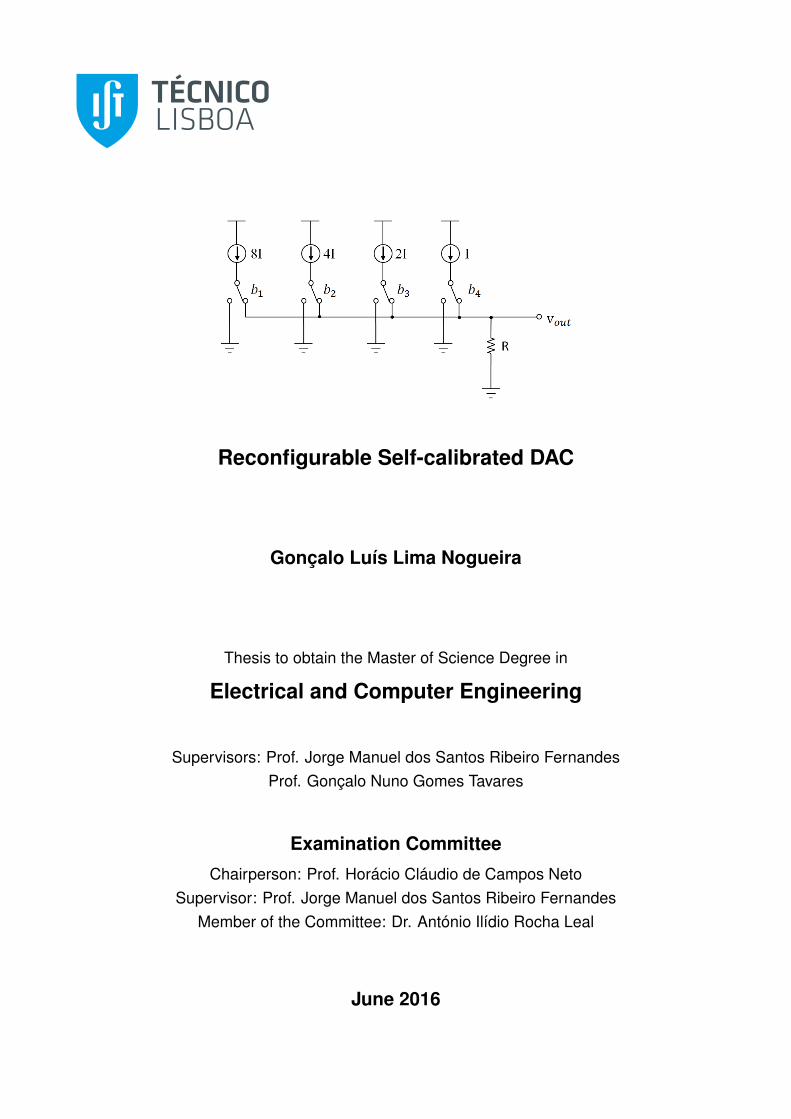
Reconfigurable Self-calibrated DAC
Gonçalo Luís Lima Nogueira
Thesis to obtain the Master of Science Degree in
Electrical and Computer Engineering
Supervisors: Prof. Jorge Manuel dos Santos Ribeiro FernandesProf. Gonçalo Nuno Gomes Tavares
Examination Committee
Chairperson: Prof. Horácio Cláudio de Campos NetoSupervisor: Prof. Jorge Manuel dos Santos Ribeiro Fernandes
Member of the Committee: Dr. António Ilídio Rocha Leal
June 2016

ii
Abstract
A new calibration method for current steering DACs based on rearranging the commutation sequence of
thermometer coded current sources, also called switching-sequence post-adjustment (SSPA) is presented.
This calibration method calculates the optimal commutation sequence that maximizes any desired per-
formance metric instead of generating it based on ad-hoc or heuristic arguments, which, while often
performing adequately are not guaranteed to attain the best solution.
The proposed calibration method has three steps: (1) sorting the thermometer coded current sources
by increasing current value, (2) measuring the current produced by each thermometer coded current
source and (3) finding the optimal commutation sequence. The second step is done with the help of an
extra current source array. An add-on is proposed, consisting on the correction of the output error in
realtime, during D/A conversion.
As a proof of concept, part of a 12-bit segmented current steering DAC is designed, using a 6-6
segmentation, and using the minimum area possible. In this work, six different simulations are run,
targeting two different performance metrics (one in each simulation), comparing the proposed calibration
algorithm to another state-of-the-art SSPA calibration method. The results show that the proposed
calibration method improves the INL up to 9 times and the ENOB up to 1.1 bit when compared to the
other.
Keywords: Calibration method, current-steering, DAC, optimal commutation sequence, reconfigurable,
SSPA
iii

iv

Resumo
Um novo metodo de calibracao para current steering DACs baseado em definir uma sequencia da co-
mutacao de fontes de corrente em codigo termometro, tambem conhecido por switching-sequence post-
adjustment (SSPA) e apresentado. Este metodo de calibracao calcula a sequencia de comutacao optima
que maximiza qualquer especificacao desejada em vez de a gerar baseada em argumentos ad-hoc ou
heuristicos, que, embora geralmente tenham bom desempenho, nao garantem a obtencao da solucao
optima.
O metodo de calibracao proposto consiste em tres passos: (1) sequenciar as fontes de corrente em
codigo termometro por ordem crescente de corrente produzida, (2) medir a corrente produzida por cada
fonte de corrente em codigo termometro e (3) procurar a sequencia de comutacao optima. O segundo
passo e realizado com a ajuda de um conjunto extra de fontes de corrente. Uma tecnica adicional e
proposta, consistindo na correccao da saıda em tempo real, durante a conversao digital/analogico.
Como prova de conceito, parte de um current steering DAC segmentado de 12 bit e construido, usando
uma segmentacao 6-6 e a mınima area possıvel. Na dissertacao sao realizadas seis simulacoes distintas,
visando duas diferentes especificacoes (uma especificacao em cada simulacao) e comparando o metodo de
calibracao proposto com um metodo de calibracao SSPA do estado da arte. Os resultados mostram que
para o metodo proposto a INL melhora ate 9 vezes e o ENOB ate 1.1 bit quando comparado com o outro
metodo.
Palavras-chave: Metodo de calibracao, current-steering, DAC, Sequencia de comutacao optima, Re-
configuravel, SSPA
v

vi
Contents
Abstract . . . . . . . . . . . . . . . . . . . . . . . . . . . . . . . . . . . . . . . . . . . . . . . . . iii
Resumo . . . . . . . . . . . . . . . . . . . . . . . . . . . . . . . . . . . . . . . . . . . . . . . . . v
List of Figures . . . . . . . . . . . . . . . . . . . . . . . . . . . . . . . . . . . . . . . . . . . . . xii
List of Tables . . . . . . . . . . . . . . . . . . . . . . . . . . . . . . . . . . . . . . . . . . . . . . xiii
List of Acronyms . . . . . . . . . . . . . . . . . . . . . . . . . . . . . . . . . . . . . . . . . . . . xv
List of Symbols . . . . . . . . . . . . . . . . . . . . . . . . . . . . . . . . . . . . . . . . . . . . . xvii
1 Introduction 1
1.1 Historical Perspective of Digital-to-Analog Converters . . . . . . . . . . . . . . . . . . . . 1
1.2 Motivation . . . . . . . . . . . . . . . . . . . . . . . . . . . . . . . . . . . . . . . . . . . . 1
1.3 Objectives . . . . . . . . . . . . . . . . . . . . . . . . . . . . . . . . . . . . . . . . . . . . . 2
1.4 Structure of the Thesis . . . . . . . . . . . . . . . . . . . . . . . . . . . . . . . . . . . . . . 3
2 Digital-to-Analog Converters 5
2.1 Basic Concepts and Architectures . . . . . . . . . . . . . . . . . . . . . . . . . . . . . . . . 5
2.1.1 Digital-to-Analog Conversion . . . . . . . . . . . . . . . . . . . . . . . . . . . . . . 5
2.1.2 Static Specifications . . . . . . . . . . . . . . . . . . . . . . . . . . . . . . . . . . . 7
2.1.3 Dynamic Specifications . . . . . . . . . . . . . . . . . . . . . . . . . . . . . . . . . 9
2.1.4 Digital-to-Analog Converter Architectures . . . . . . . . . . . . . . . . . . . . . . . 12
2.1.5 Segmented Current-Steering DAC’s Customization . . . . . . . . . . . . . . . . . . 16
2.2 Commutation Sequences for Thermometer-Coded Current-Steering DAC Calibration . . . 19
2.2.1 Hierarchical Symmetrical Resequencing . . . . . . . . . . . . . . . . . . . . . . . . 20
2.2.2 State-of-the-Art Resequencing . . . . . . . . . . . . . . . . . . . . . . . . . . . . . . 22
2.3 Specifications of the developed DAC . . . . . . . . . . . . . . . . . . . . . . . . . . . . . . 22
2.3.1 Correction Block . . . . . . . . . . . . . . . . . . . . . . . . . . . . . . . . . . . . . 24
2.3.2 Extra Current Sources in the MSB Current Source Array . . . . . . . . . . . . . . 29
2.3.3 Comparator Block . . . . . . . . . . . . . . . . . . . . . . . . . . . . . . . . . . . . 32
3 Analog Circuits 33
3.1 MSB Current Source Array . . . . . . . . . . . . . . . . . . . . . . . . . . . . . . . . . . . 33
3.2 Comparator Block . . . . . . . . . . . . . . . . . . . . . . . . . . . . . . . . . . . . . . . . 40
3.2.1 Architecure . . . . . . . . . . . . . . . . . . . . . . . . . . . . . . . . . . . . . . . . 40
vii
3.2.2 Sampling . . . . . . . . . . . . . . . . . . . . . . . . . . . . . . . . . . . . . . . . . 45
3.2.3 Calibration of the Offset Voltage . . . . . . . . . . . . . . . . . . . . . . . . . . . . 46
4 MSB Current Source’s Sorting Algorithm 49
4.1 Data Acquisition . . . . . . . . . . . . . . . . . . . . . . . . . . . . . . . . . . . . . . . . . 49
4.2 Optimal Commutation Sequence . . . . . . . . . . . . . . . . . . . . . . . . . . . . . . . . 54
4.2.1 MSB Commutation Sequence . . . . . . . . . . . . . . . . . . . . . . . . . . . . . . 54
4.2.2 Current Source Correction . . . . . . . . . . . . . . . . . . . . . . . . . . . . . . . . 65
4.3 Output Current Characteristic . . . . . . . . . . . . . . . . . . . . . . . . . . . . . . . . . 71
5 Conclusions 79
5.1 Final Conclusions . . . . . . . . . . . . . . . . . . . . . . . . . . . . . . . . . . . . . . . . . 79
5.2 Future Work . . . . . . . . . . . . . . . . . . . . . . . . . . . . . . . . . . . . . . . . . . . 80
Bibliography 82
A Simulation Results 83
A.1 Simulation Results from Subsection 4.2.1 . . . . . . . . . . . . . . . . . . . . . . . . . . . 83
A.2 Simulation Results from Subsection 4.2.2 . . . . . . . . . . . . . . . . . . . . . . . . . . . 85
A.3 Simulation Results from Section 4.3 . . . . . . . . . . . . . . . . . . . . . . . . . . . . . . 86
viii
List of Figures
2.1 Analog and digital signals . . . . . . . . . . . . . . . . . . . . . . . . . . . . . . . . . . . . 6
2.2 Simple DAC scheme . . . . . . . . . . . . . . . . . . . . . . . . . . . . . . . . . . . . . . . 6
2.3 Input and output signals of a DAC . . . . . . . . . . . . . . . . . . . . . . . . . . . . . . . 6
2.4 DAC output characteristic . . . . . . . . . . . . . . . . . . . . . . . . . . . . . . . . . . . . 7
2.5 Offset and gain errors in an output characteristic of a DAC . . . . . . . . . . . . . . . . . 8
2.6 Real output characteristic of a DAC and the correspondent INL . . . . . . . . . . . . . . . 8
2.7 Real output characteristic of a DAC and the correspondent DNL . . . . . . . . . . . . . . 9
2.8 Step response of a second-order system . . . . . . . . . . . . . . . . . . . . . . . . . . . . . 10
2.9 Output signal of an input count up sequence with an occurrence of a glitch . . . . . . . . 10
2.10 Resistor-string with n-channel switches and a tree-like decoder 3-bit DAC . . . . . . . . . 12
2.11 Binary weighted resistors 4-bit DAC . . . . . . . . . . . . . . . . . . . . . . . . . . . . . . 13
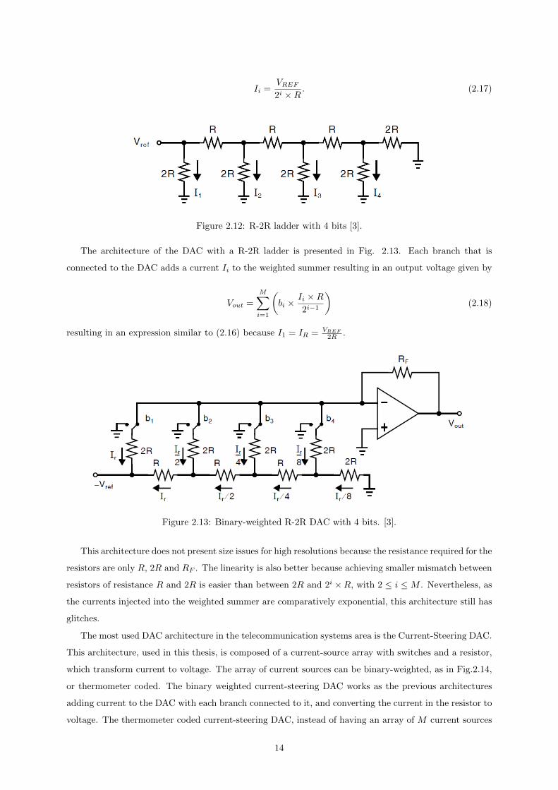
2.12 R-2R ladder with 4 bits . . . . . . . . . . . . . . . . . . . . . . . . . . . . . . . . . . . . . 14
2.13 Binary-weighted R-2R DAC with 4 bits . . . . . . . . . . . . . . . . . . . . . . . . . . . . 14
2.14 Binary-Weighted Current-Steering DAC with 4 bits . . . . . . . . . . . . . . . . . . . . . . 15
2.15 Advantages and disadvantages of binary weighted, thermometer coded and segmented DAC
architectures . . . . . . . . . . . . . . . . . . . . . . . . . . . . . . . . . . . . . . . . . . . 16
2.16 100 MATLAB simulation results for thermometer-coded versus binary-weighted DACs . . 17
2.17 Normalized required area vs percentage of segmentation . . . . . . . . . . . . . . . . . . . 17
2.18 Resenquencing of the current sources . . . . . . . . . . . . . . . . . . . . . . . . . . . . . . 18
2.19 Calibration process . . . . . . . . . . . . . . . . . . . . . . . . . . . . . . . . . . . . . . . . 19
2.20 Simulation results for optimization of the number of extra current sources . . . . . . . . . 20
2.21 Hierarchical symmetrical sequence . . . . . . . . . . . . . . . . . . . . . . . . . . . . . . . 21
2.22 Hierarchical symmetrical mirror sequence . . . . . . . . . . . . . . . . . . . . . . . . . . . 21
2.23 Hierarchical symmetrical mirror sequence for telecommunications . . . . . . . . . . . . . . 23
2.24 Performance results for the sorting algorithm in [1] . . . . . . . . . . . . . . . . . . . . . . 23
2.25 Block diagram of the DAC system . . . . . . . . . . . . . . . . . . . . . . . . . . . . . . . 24
2.26 Current values of the sorted current source array and respective error intervals . . . . . . 28
2.27 Histogram with the correction higher than 2 LSB needed in 10000 MSB current source
arrays while using the sorting algorithm with correction . . . . . . . . . . . . . . . . . . . 28
ix
2.28 σI
I of the current sources in a MSB current source array as a function of the number of
extra current sources while maintaining a DNL of 2 LSB with a 99% yield . . . . . . . . . 29
2.29 Relative area in function of the number of extra current sources . . . . . . . . . . . . . . . 31
2.30 Structure of the comparator block . . . . . . . . . . . . . . . . . . . . . . . . . . . . . . . 32
3.1 Designed current source . . . . . . . . . . . . . . . . . . . . . . . . . . . . . . . . . . . . . 34
3.2 DAC simplified output impedance equivalent circuit . . . . . . . . . . . . . . . . . . . . . 36
3.3 Designed decoding circuit . . . . . . . . . . . . . . . . . . . . . . . . . . . . . . . . . . . . 37
3.4 Testbench circuit used for the simulations . . . . . . . . . . . . . . . . . . . . . . . . . . . 38
3.5 Result of the 500 monte carlo simulations . . . . . . . . . . . . . . . . . . . . . . . . . . . 39
3.6 Output current produced by the current source cell as a function of the output voltage . . 39
3.7 Schematic of the circuit of the comparator used in this work . . . . . . . . . . . . . . . . . 41
3.8 Voltages in the comparator as a function of time during operation . . . . . . . . . . . . . 41
3.9 Bit error rate of a 204 µV input referred noise comparator as a function of the input offset
voltage and simulation results . . . . . . . . . . . . . . . . . . . . . . . . . . . . . . . . . . 44
3.10 Circuit of the input of the comparator block, where the current is amplified, converted to
voltage, sampled and hold . . . . . . . . . . . . . . . . . . . . . . . . . . . . . . . . . . . . 45
3.11 Circuit used as variable capacitors in Fig.3.7 (C2) . . . . . . . . . . . . . . . . . . . . . . . 47
3.12 Variation of gate-source and gate-drain capacitances versus VGS . . . . . . . . . . . . . . 47
4.1 Plot of the current generated by each MSB current source, following the pointer array
sequence before step 1 . . . . . . . . . . . . . . . . . . . . . . . . . . . . . . . . . . . . . . 50
4.2 Plot of the current generated by each MSB current source, following the pointer array
sequence after step 1 . . . . . . . . . . . . . . . . . . . . . . . . . . . . . . . . . . . . . . . 51
4.3 Plot of the current generated by each MSB current source, following the pointer array
sequence, and difference interval limits after step 2 . . . . . . . . . . . . . . . . . . . . . . 52
4.4 Source queue flowchart . . . . . . . . . . . . . . . . . . . . . . . . . . . . . . . . . . . . . . 59
4.5 Optimal queue flowchart . . . . . . . . . . . . . . . . . . . . . . . . . . . . . . . . . . . . . 59
4.6 Number of marked vertices in the optimal queue as a function of the optimal queue dimension 60
4.7 Mean optimal value at the end of the search as a function of the optimal queue dimension 61
4.8 Mean simulated INL of 1000 MSB current source arrays using this work’s sorting algorithm
as a function of the comparator’s input referred noise voltage . . . . . . . . . . . . . . . . 62
4.9 Mean simulated INL of 1000 MSB current source arrays using the sorting algorithm in [1]
sorting algorithm as a function of the comparator’s input referred noise voltage . . . . . . 62
4.10 Quantization noise producing circuit . . . . . . . . . . . . . . . . . . . . . . . . . . . . . . 63
4.11 Example graph of VQ(t) if the data converters of Fig.4.10 were ideal . . . . . . . . . . . . 63
4.12 Mean simulated ENOB of 1000 MSB current source arrays for a fullscale signal using this
work’s sorting algorithm as a function of the comparator’s input referred noise voltage . . 65
4.13 Mean simulated ENOB of 1000 MSB current source arrays for a fullscale signal using the
sorting algorithm in [1] as a function of the comparator’s input referred noise voltage . . . 65
x
4.14 Mean simulated INL of 1000 MSB current source arrays using this work’s sorting algorithm
implemented with correction as a function of the comparator’s input referred noise voltage 70
4.15 Mean simulated INL of 1000 MSB current source arrays using the sorting algorithm in [1]
implemented with correction as a function of the comparator’s input referred noise voltage 70
4.16 Mean simulated ENOB of 1000 MSB current source arrays for a fullscale signal using this
work’s sorting algorithm implemented with correction as a function of the comparator’s
input referred noise voltage . . . . . . . . . . . . . . . . . . . . . . . . . . . . . . . . . . . 70
4.17 Mean simulated ENOB of 1000 MSB current source arrays for a fullscale signal using the
sorting algorithm in [1] implemented with correction as a function of the comparator’s
input referred noise voltage . . . . . . . . . . . . . . . . . . . . . . . . . . . . . . . . . . . 71
4.18 Average output current characteristic of a MSB current source as a function of the input
code Din of the DAC . . . . . . . . . . . . . . . . . . . . . . . . . . . . . . . . . . . . . . . 72
4.19 Output current error deviation characteristic of a MSB current source as a function of the
input code Din of the DAC . . . . . . . . . . . . . . . . . . . . . . . . . . . . . . . . . . . 73
4.20 Estimated output current error average characteristic of the DAC as a function of the input
code Din . . . . . . . . . . . . . . . . . . . . . . . . . . . . . . . . . . . . . . . . . . . . . . 73
4.21 Mean simulated INL of 1000 MSB current source arrays using this work’s sorting algorithm
implemented with correction as a function of the comparator’s input referred noise voltage 75
4.22 Mean simulated INL of 1000 MSB current source arrays using this work’s sorting algorithm
implemented without correction as a function of the comparator’s input referred noise voltage 75
4.23 Mean simulated INL of 1000 MSB current source arrays using the sorting algorithm in
[1] implemented without correction as a function of the comparator’s input referred noise
voltage . . . . . . . . . . . . . . . . . . . . . . . . . . . . . . . . . . . . . . . . . . . . . . . 76
4.24 Mean simulated ENOB of 1000 MSB current source arrays for a fullscale signal using this
work’s sorting algorithm implemented with correction as a function of the comparator’s
input referred noise voltage . . . . . . . . . . . . . . . . . . . . . . . . . . . . . . . . . . . 76
4.25 Mean simulated ENOB of 1000 MSB current source arrays for a fullscale signal using this
work’s sorting algorithm implemented without correction as a function of the comparator’s
input referred noise voltage . . . . . . . . . . . . . . . . . . . . . . . . . . . . . . . . . . . 76
4.26 Mean simulated ENOB of 1000 MSB current source arrays for a fullscale signal using the
sorting algorithm in [1] implemented without correction as a function of the comparator’s
input referred noise voltage . . . . . . . . . . . . . . . . . . . . . . . . . . . . . . . . . . . 77
A.1 Worstcase simulated INL of 1000 MSB current source arrays using this work’s sorting
algorithm as a function of the comparator’s input referred noise voltage . . . . . . . . . . 83
A.2 Worstcase simulated INL of 1000 MSB current source arrays using the sorting algorithm
in [1] as a function of the comparator’s input referred noise voltage . . . . . . . . . . . . . 84
xi

A.3 Mean simulated ENOB of 1000 MSB current source arrays for a −3 dB fullscale signal
using this work’s sorting algorithm as a function of the comparator’s input referred noise
voltage . . . . . . . . . . . . . . . . . . . . . . . . . . . . . . . . . . . . . . . . . . . . . . . 84
A.4 Mean simulated ENOB of 1000 MSB current source arrays for a −3 dB fullscale signal
using the sorting algorithm in [1] as a function of the comparator’s input referred noise
voltage . . . . . . . . . . . . . . . . . . . . . . . . . . . . . . . . . . . . . . . . . . . . . . . 84
A.5 Worstcase simulated INL of 100 MSB current source arrays using this work’s sorting algo-
rithm implemented with correction as a function of the comparator’s input referred noise
voltage . . . . . . . . . . . . . . . . . . . . . . . . . . . . . . . . . . . . . . . . . . . . . . . 85
A.6 Worstcase simulated INL of 1000 MSB current source arrays using the sorting algorithm
in [1] implemented with correction as a function of the comparator’s input referred noise
voltage . . . . . . . . . . . . . . . . . . . . . . . . . . . . . . . . . . . . . . . . . . . . . . . 85
A.7 Mean simulated ENOB of 1000 MSB current source arrays for a −3 dB fullscale signal using
this work’s sorting algorithm implemented with correction as a function of the comparator’s
input referred noise voltage . . . . . . . . . . . . . . . . . . . . . . . . . . . . . . . . . . . 85
A.8 Mean simulated ENOB of 1000 MSB current source arrays for a −3 dB fullscale signal using
the sorting algorithm implemented in [1] with correction as a function of the comparator’s
input referred noise voltage . . . . . . . . . . . . . . . . . . . . . . . . . . . . . . . . . . . 86
A.9 Mean simulated ENOB of 1000 MSB current source arrays for a fullscale signal using this
work’s sorting algorithm, implemented without correction and improving the INL, as a
function of the comparator’s input referred noise voltage . . . . . . . . . . . . . . . . . . . 86
A.10 Mean simulated ENOB of 1000 MSB current source arrays for a fullscale signal using
this work’s sorting algorithm, implemented with correction and improving the INL, as a
function of the comparator’s input referred noise voltage . . . . . . . . . . . . . . . . . . . 86
A.11 Mean simulated ENOB of 1000 MSB current source arrays for a −3 dB fullscale signal
using this work’s sorting algorithm implemented without correction as a function of the
comparator’s input referred noise voltage . . . . . . . . . . . . . . . . . . . . . . . . . . . 87
A.12 Mean simulated ENOB of 1000 MSB current source arrays for a −3 dB fullscale signal
using the sorting algorithm in [1] implemented without correction as a function of the
comparator’s input referred noise voltage . . . . . . . . . . . . . . . . . . . . . . . . . . . 87
A.13 Mean simulated ENOB of 1000 MSB current source arrays for a −3 dB fullscale signal using
this work’s sorting algorithm implemented with correction as a function of the comparator’s
input referred noise voltage . . . . . . . . . . . . . . . . . . . . . . . . . . . . . . . . . . . 87
A.14 Mean simulated INL of 1000 MSB current source arrays using this work’s sorting algo-
rithm, implemented without correction and improving the ENOB, as a function of the
comparator’s input referred noise voltage . . . . . . . . . . . . . . . . . . . . . . . . . . . 88
A.15 Mean simulated INL of 1000 MSB current source arrays using this work’s sorting algorithm,
implemented with correction and improving the ENOB, as a function of the comparator’s
input referred noise voltage . . . . . . . . . . . . . . . . . . . . . . . . . . . . . . . . . . . 88
xii
List of Tables
2.1 Transistor dimensions, current variation and relative area as a function of the number of
extra current sources resultant from the global optimization . . . . . . . . . . . . . . . . . 31
3.1 Process parameters . . . . . . . . . . . . . . . . . . . . . . . . . . . . . . . . . . . . . . . . 35
3.2 Dimensions of the transistors of the MSB current source cell . . . . . . . . . . . . . . . . . 38
3.3 Dimensions of the transistors of the MSB current source cell after adding the extra current
sources . . . . . . . . . . . . . . . . . . . . . . . . . . . . . . . . . . . . . . . . . . . . . . . 39
3.4 Dimensions of the transistors of the comparator circuit, except for the variable capacitors
C2 . . . . . . . . . . . . . . . . . . . . . . . . . . . . . . . . . . . . . . . . . . . . . . . . . 44
3.5 Dimensions of the transistors inside variable capacitor C2 . . . . . . . . . . . . . . . . . . 48
4.1 Current sources data: current sources and initial respective difference . . . . . . . . . . . 51
4.2 Current sources data: current sources by ascending current value . . . . . . . . . . . . . . 52
4.3 Current sources data: current sources by ascending current value and respective difference 53
4.4 Current sources data: current sources by ascending current value and respective estimated
difference to the master current source . . . . . . . . . . . . . . . . . . . . . . . . . . . . . 55
4.5 Current sources data: current sources by ascending current value and respective estimated
DNL error . . . . . . . . . . . . . . . . . . . . . . . . . . . . . . . . . . . . . . . . . . . . . 56
4.6 Current sources pairs data: Pairs and respective estimated DNL error . . . . . . . . . . . 57
4.7 Pair and DAC’s commutation sequence . . . . . . . . . . . . . . . . . . . . . . . . . . . . . 60
4.8 Current sources data: current sources by ascending current value, respective estimated
DNL error and number of dstep used to correct each current source . . . . . . . . . . . . . 66
4.9 Current sources data for the algorithm in [1] implemented with correction: current sources
by ascending current value, respective estimated DNL error and number of dstep used to
correct each current source . . . . . . . . . . . . . . . . . . . . . . . . . . . . . . . . . . . 67
4.10 Current sources data: pairs and respective estimated pair DNL error . . . . . . . . . . . . 67
4.11 Current sources data: pair and DAC’s commutation sequence and respective number of
dstep used to correct the current source . . . . . . . . . . . . . . . . . . . . . . . . . . . . . 68
4.12 Current sources data: pair and DAC’s commutation sequence and respective number of
dstep used to correct the current source plus the secondary correction array . . . . . . . . 69
4.13 Current sources data: pair and DAC’s commutation sequence and individual code correction 69
xiii

xiv

List of Acronyms
Acronym Description
ADC Analog-to-Digital Converter
CMOS Complementary Metal-Oxide-Semiconductor
DAC Digital-to-Analog Converter
DNL Differential Nonlinearity
DFT Direct Fourier Transform
ENOB Effective Number of Bits
FFT Fast Fourier Transform
INL Integral Nonlinearity
LSB Least Significant Bit
MIMCAP Metal-Insulator-Metal Capacitor
MOMCAP Metal-Oxide-Metal Capacitor
NMOS n-channel Metal-Oxide-Semiconductor
PMOS p-channel Metal-Oxide-Semiconductor
OPAMP Operational Amplifier
MOSFET Metal-Oxide-Semiconductor Field Effect Transistor
MSB Most Significant Bit
RAM Random Access Memory
SSPA Switching-Sequence Post-Adjustment
SNDR Signal to Noise and Distortion Ratio
SFDR Spurious Free Dynamic Range
SNR Signal-to-Noise Ratio
THD Total Harmonic Distortion
xv

xvi

List of Symbols
Symbol Description
α Standard deviation input increase by standard deviation capacitance in-
crease
γ Coefficient dependent of the transistors drain to source voltage and sizes
(used in thermal noise)
µ Carrier mobility
µ(X) Mean value of the random variable X
µCox HS Electron mobility multiplied by the gate oxide transistor of the high speed
transistor
µCox HS LV Electron mobility multiplied by the gate oxide transistor of the high speed
low Vth transistor
σ Sigma
σcap standard deviation of the capacitor due to process variations
σI/I Relative standard deviation of the current produced by a current source
σI0 Standard deviation of the current of a current source in the array without
extra current sources
σI1 Standard deviation of the current of a current source in the array with extra
current sources
σoffset standard deviation of the input referred noise voltage of the comparator
σ(X) Standard deviation of the random variable X
τ0 Differential’s pair time constant
∆ Quantization step
∆MSB MSB quantization step
A0 Occupied area by the current source array without the extra current sources
A1 Occupied area by the current source array with the extra current sources
Aβ Matching property of a MOSFET determined by fluctuations in the electron
mobility
Acst Area of the designed current source transistor
Ai Amplitude of the bin i in a DFT or FFT
xvii

Are Area occupied by a MSB current source, except for the current source tran-
sistor
AVthMatching property of a MOSFET determined by the gate oxide thickness
Aun Area occupied by a current source (Unity)
bi Digital value of the bit i
bin(f) Number of the bin in the DFT or FFT correspondent to the frequency f
bin max() Number of the bin in the DFT or FFT correspondent to the spectrum
component with the highest amplitude value
Cnk n choose k
Cox Gate oxide capacitance
CSG Source to gate capacitance
dB Decibel
dDin Digital input word Din
dest Array with the approximate mean difference of the MSB current sources
Din Value of the input word of the DAC
dmes Measured difference Array
DNLpair DNL of a current steering DAC that pairs current sources, applying dither-
ing
DNLsingle DNL of a current steering DAC that does not pair current sources or applies
dithering teechniques
dstep Unit equal to 2−5 LSB of current
e(i,j) Error produced by the pair (i,j)
ek Error current of a current source due to process variations
e′k(Din) Current error of the MSB current source k, when the input code is Din, due
to its finite output impedance
eLSB Sum of all the current error of the LSB current source in a segmented current
steering DAC when they are disabled
emax Current error of the current source with the biggest absolute error value in
the array
ep Mean error current of a pair of current sources
ep max Mean error current of the pair of current sources with the highest absolute
mean error
erandom Current error of a random current source from the array
es max Maximum current error value of the absolute value of the sum of ep with
eLSB
fin Fundamental frequency of the input signal
xviii
fobj Objective function
gds Drain to source conductance
gm Transconductance
H Number of harmonics measured
i General index
I Current produced by a current source
ID Current produced by the number of current sources connected to the dummy
load
IDS Current driven from the drain to the source
Ik Current produced by the current source k
IMSB Current generated by a MSB current source
IO Current produced by the current sources connected to the output
Iout(Din) Current at the output of a current DAC when the input code is Din
IREF Reference current value
ISD Current driven from source to drain
k Current source index
L Length of a transistor
LCS Length of the current source transistor in the MSB current source
LCAS Length of the cascode transistor in the MSB current source
Lmin minimum length of a transistor
M Resolution of a DAC measured in bits
n General index
N Number of codes
NBW Equivalent noise bandwidth
ncs Number of current sources in the current source array
nD Number of current sources connected to the dummy load
ndif Array containing in each position the number of current sources that have
the same
ndif smaller Array containing in each position the number of current sources that have
the same dmes value as the one pointed and that have smaller current than
the pointed current source
nextra Number of extra current sources in the current source array
nO Number of current sources connected to the output load
p Pair index
xix
Pextra cs(n, i, psuc) Probability of having n sucesses out of n+i independent yes/no experiments,
knowing the probability of success psuc
PD Distortion power of a signal
PN Noise power of a signal
Pfullscale Power of a sampled fullscale signal
Pquant N Quantization power noise
PS Power of the sampled signal
psuc Probability of having a success in a yes/no experiment
˜psuc Approximate probability of having a success in a yes/no experiment
Rout Resistance of the output resistor
round(x) Integer closer to the value x. In case x has a fractional part of 0.5, then
round(x) is the integer closer to x with the largest value
S General set
Sn Symmetric group
sout Output signal of a generic DAC
sout,ideal Ideal output signal fo a generic DAC
SREF Reference signal for a generic DAC
ti Integration time in the comparator during a comparison
Ts Time interval
VCAOVOverdrive voltage of the cascode transistor
VCSOVOverdrive voltage of the current source transistor
Vdd Supply voltage
VDS Drain to source voltage drop
VDSswitchDrain to source voltage drop of the switch transistor
VGS Gate to source voltage drop
VIN Voltage at the input N of the comparator
VIP Voltage at the input P of the comparator
Vmar sat Saturation margin voltage
vn Root mean square noise voltage
Vnode(i) Voltage in the node i
VON Voltage at the output N of the comparator
VOP Voltage at the output P of the comparator
Vout Output Voltage
Vout swing Output swing voltage
VOV Overdrive voltage
VREF Reference voltage
VSD Source to drain voltage drop
xx

VSG Source to gate voltage drop
Vth Threshold voltage
Y General set
X Random variable
W Width of a transistor
WCAS Width of the cascode transistor in the MSB current source
WCAS SW Width of the switch cascode transistor in the MSB current source
WCS Width of the current source transistor in the MSB current source
Wmin Minimum width of a transistor
WSW Width of the switch transistor in the MSB current source
ZD Output impedance of the current sources connected to the dummy load
ZDkOutput impedance of the current source k connected to the dummy load
ZL Load impedance
ZO Output impedance of the current sources connected to the output
ZOkOutput impedance of the current source k connected to the output
xxi

xxii
Chapter 1
Introduction
In this chapter the proposed work is presented. In section 1.1 the Digital-to-Analog Converter’s (DAC)
relevance in today’s applications is presented, followed by section 1.2 which presents the motivation for
the development of this work. In section 1.3 the objectives for this thesis are presented, introducing its
theme and presenting the goals to be pursued, and for last, in section 1.4 a brief presentation of the
structure of the thesis is made.
1.1 Historical Perspective of Digital-to-Analog Converters
Telecommunications and electronics are wide areas that make extensive use of contemporary circuits
and signal processing algorithms. As the signal processing on these areas occur mainly in the digital
domain and the input and output is mainly analog, the use of an Analog-to-Digital Converter (ADC)
and a Digital-to-Analog Converter (DAC) is needed to do the bridge between the inputs, outputs and
processing unit.
With the increase of the mobile market the need for die area reduction as well as power consumption
has increased, making the development of techniques to improve the performance of converter circuits
one of the main areas of development in the present-day. In order to achieve moderate resolutions for
communications while maintaining a small area, calibration techniques are used to make up for the process
deviations of Metal-Oxide-Semiconductor Field Effect Transistors (MOSFET).
1.2 Motivation
Segmented current-steering DACs with calibration using commutation sequences, which belong to the
state-of-the-art of telecommunication electronic systems, sort the current sources by increasing current
value and apply commutation sequences to the MSB current source array to improve the Differential
NonLinearity (DNL) and Integral NonLinearity (INL). These commutation sequences are based on ad-
hoc or heuristic arguments, which, while often performing adequately, are not guaranteed to attain the
best solution. As so, there is no literature on finding an optimal commutation sequence to apply to a
MSB current source array, or on measuring the difference of current between MSB current sources and
1
use that information to calculate a commutation sequence that improves the INL, the DNL or any other
performance the most. There is also no literature on using the latter together with current sources that
correct the output as desired.
As so, in this work, the current produced by each current source in the MSB current source array is
quantized and an optimal algorithm to obtain the optimal commutation sequence and error correction
targeting the improvement of a desired performance applied, which can be the INL, the Total Harmonic
Distortion (THD), the Signal-to-Noise Ratio (SNR), the Signal-to-Noise and Distortion Ratio (SNDR),
the even or odd harmonic distortion or a weighted-function composed of any of these specifications.
1.3 Objectives
The main objective of this work is to develop and design an algorithm that calculates the optimal
commutation sequence for a DAC, targeting any performance, with the possibility of being reconfigured
at any time. The secondary objective of this work is to test the algorithm by designing a DAC or part of
one, implementing the algorithm and performing tests to verify different performances.
To design the DAC the use of three current source arrays, a resistor, a comparator and a digital
system is needed. The MSB and LSB current source arrays and the resistor are part of the current-
steering digital-to-analog conversion method; the other current source array, which will be denominated
by correction current source array, is used to measure the difference of current between MSB current
sources and correct the error present in the output during digital-to-analog conversion; the comparator
detects, between two input currents, which one is higher; the digital system controls the DAC operations
and stores the optimal commutation sequence for a desired performance. This system is not designed in
this thesis, as it is not needed to test the algorithm.
In this work it will be considered that there is a processing unit, outside the DAC’s chip, that
communicates with the DAC, processes information and computes the optimal commutation sequence.
If the DAC is in an embedded system, then a processing unit is usually available and the calibration
program can be put in it, saving space in the chip. The digital system of the DAC has a writable memory
unit to address current sources, so, if a non-volatile memory is used, the microprocessor that computes
the optimal commutation sequence can calibrate the DAC upon fabrication, being removed or changed
after, if needed. This process allows the DAC to be calibrated after production, being only vulnerable to
aging effects. Calibration can be performed again if the processing unit to which the DAC is connected
to after production has the calibration program.
In order to reduce area the MSB current array is designed with extra but smaller current sources that
maintain the DAC’s performance. With this approach, of all current sources in the MSB current source
array only the ones that improve the performance of the DAC optimally are used.
In the algorithm the MSB current sources are sorted by increasing current value, being the median
defined as the master current source and the difference of current between each current source and the
master current source measured. To measure this difference, current sources from the correction current
source array are enabled in parallel with the master current source and compared to a MSB current
2
source. The algorithm that finds the optimal commutation sequence combines permutations and graph
theory, where the set of all commutation sequences is described as a graph. In this graph the commutation
sequence that minimizes a desired performance is searched, and when found used. The algorithm can
also implement correction while searching. If correction is used, then, after the optimal commutation
sequence has been found, the current sources in the correction current source array correct the output
error as the output is generated.
In the end it is expected to obtain an INL and DNL below 1 Least Significant Bit (LSB) and an
Effective Number of Bits (ENOB) above 11.5 bits with the designed 12 bit DAC blocks.
1.4 Structure of the Thesis
This thesis is divided in 5 chapters, being a small description of the following chapters presented in the
next paragraphs.
The second chapter of this thesis presents DACs: some basic concepts and architectures, a revision of
the state-of-the-art and the specifications of the developed DAC blocks.
The third chapter of this thesis presents the developed analog circuits inside the DAC’s chip, explaining
how each part was dimensioned.
The fourth chapter explains the sorting algorithm used to calibrate this DAC and presents results
of simulations done with the sorting algorithms created, comparing the results with another sorting
algorithm.
The fifth chapter presents conclusions on the work developed on this thesis and recommendations of
future work to develop.
3

4
Chapter 2
Digital-to-Analog Converters
In this chapter Digital-to-Analog Converters are presented. Firstly, in section 2.1 some basic concepts
and architectures of DACs are presented, along with a calibration method used in DACs with the same
architecture used in this work. Then, in section 2.2 a review of commutation sequences for calibrating
thermometer-coded or segmented current-steering DACs is made, being also presented the commutation
sequence that is used to compare with this work. The last section presents the specifications of the DAC
developed in this work, explaining its architecture and how it is projected.
2.1 Basic Concepts and Architectures
2.1.1 Digital-to-Analog Conversion
A DAC is an electronic circuit that converts digital signals to analog signals. Signals are mathematical
representations of a function of one or more independent variables. The analog output signal used in a
DAC is either a voltage or a current and is usually represented as a function of time. The digital input
signal used in a DAC is Boolean and is usually represented as a function of time. An analog signal is a
signal that is continuous in the amplitude and time domain. On the other hand, a digital signal is a signal
that is discrete in the amplitude and time domain, that is, the signals are only described at discrete times
with limited Boolean values. In Fig.2.1 two signals, one analog and the other digital are represented.
In a DAC the conversion is made by putting digital words (d0, d1 , ... ,dN ) of M bits (bM−1...b1b0),
with N = 2M − 1 and bM−1 the MSB, at the input of the circuit as seen in Fig.2.2.
The output is then generated as a voltage or current value given by the expression
sout =Din
2MSREF (2.1)
where sout is the output’s signal value, Din is the input word’s value and SREF is the reference signal’s
value. The value of Din is calculated based on the digital word using
Din =
M−1∑i=0
bi × 2i (2.2)
5

(a) Analog signal (b) Digital signal
Figure 2.1: (a) Analog and (b) digital signals [2].
Figure 2.2: Simple DAC scheme.
with bi the value of bit i. As sout cannot be higher than SREF , Din is limited and varies from 0 to N .
The digital word at the input of the DAC is altered only at discrete values of time remaining unaltered
during an interval of time, Ts, correspondent to a period of operation of the DAC, as in Fig.2.1. This
means that the output signal of the DAC will be constant during intervals of time Ts and performs steps
at values multiples of Ts as seen in Fig. 2.3
(a) Input signal (b) Output signal
Figure 2.3: (a) Input and (b) output signals of a DAC [2].
The ideal output characteristic of a DAC is given by expression (2.1) and is represented in Fig.2.4.
6
The quantization step, ∆, is the resolution of the output signal, that is, the difference between the value
of the output signals of two adjacent words and ideally is calculated as
∆ =SREF
2M. (2.3)
Despite these basic ideal concepts, a real DAC has non-linearities which change its output character-
istic. This will be addressed in the next two subsections.
Figure 2.4: DAC output characteristic.
2.1.2 Static Specifications
Static specifications in a DAC are specifications that can be measured with static tests, that is, without the
need to have an input variable in time, like a sinusoidal signal. The static specifications used to measure
DACs’ performance are Offset Error, Gain Error, Differential Nonlinearity (DNL), Integral Nonlinearity
(INL), Monotonicity and Resolution. The offset and gain errors, DNL and INL are measured in Least
Significant Bits (LSB) and these are measured relatively to the value of ∆.
The resolution of a DAC is the value of M , that is, the number of bits in the input digital words of
the DAC. The precision of the generated output signal increases with the resolution.
The offset error corresponds to the output value when Din = 0 and the gain error corresponds to the
difference between the value at the output in the ideal DAC and the value at the output in the real DAC,
when Din = 2M − 1 and the offset error has been reduced to zero. A graphical illustration of these errors
can be seen in Fig.2.5.
The INL corresponds to the deviation from a straight line, the one that the output of the ideal DAC
should follow. This line can be chosen as the one that minimizes the maximum difference of all the codes
but for a more conservative measure the line used is the one that connects the endpoints of sout[3]. The
INL is matematically described by
INL(Din) =sout(Din)− sout,ideal(Din)
∆(2.4)
7
Figure 2.5: Offset and gain errors in an output characteristic of a DAC.
where sout,ideal(Din) is the ideal output value when the input is Din and with 0 ≤ Din ≤ 2M − 1. If the
conservative measure is adopted, the line used is
sout,ideal(Din) = Din ×∆ + sout(0) (2.5)
with
∆ =sout(2
M − 1)− sout(0)
2M − 1. (2.6)
In Fig.2.6 a real output characteristic of a DAC and its correspondent INL can be observed.
Figure 2.6: Real output characteristic of a DAC and the correspondent INL (left and right respectively).
The DNL is the difference value at the output of two adjacent digital words in regard to the quanti-
zation step ∆. It is mathematically described by
DNL(Din) =sout(Din)− sout(Din − 1)−∆
∆(2.7)
8
with 1 ≤ Din ≤ 2M − 1.
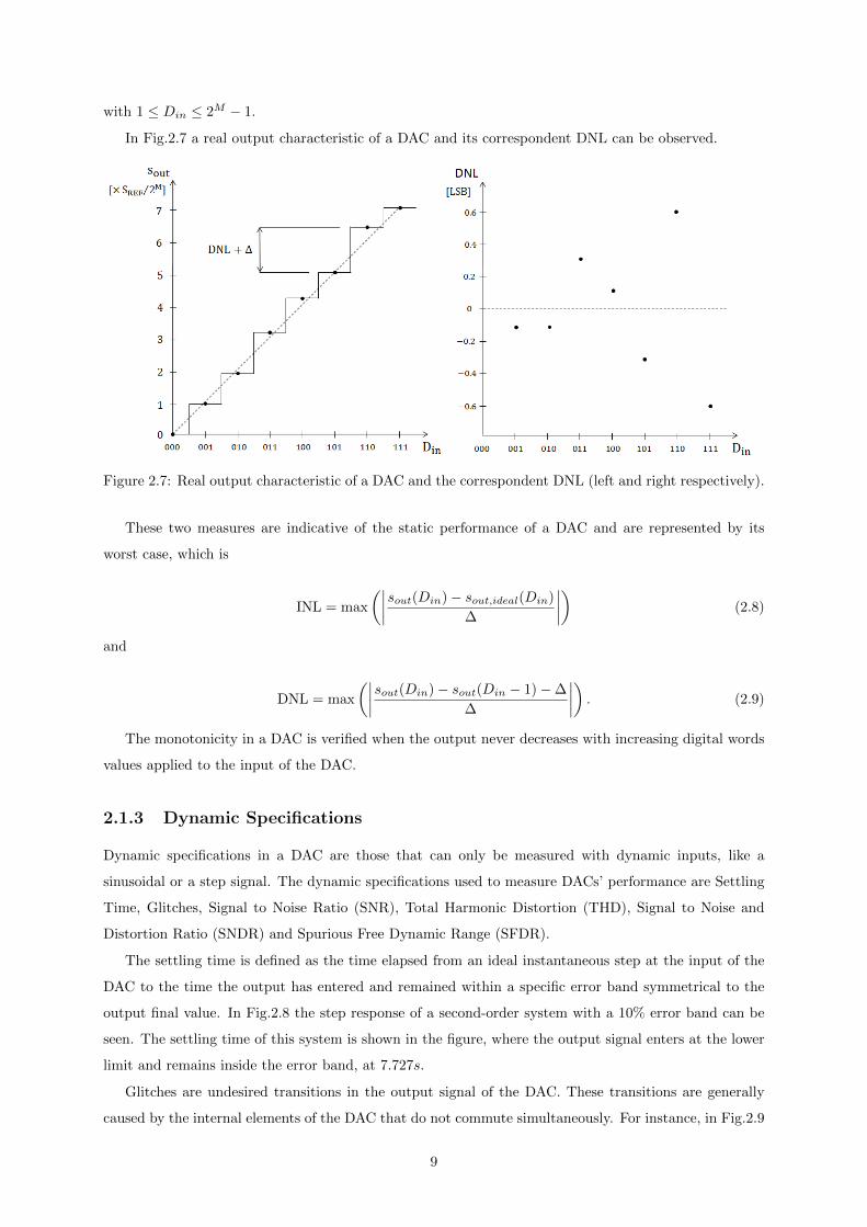
In Fig.2.7 a real output characteristic of a DAC and its correspondent DNL can be observed.
Figure 2.7: Real output characteristic of a DAC and the correspondent DNL (left and right respectively).
These two measures are indicative of the static performance of a DAC and are represented by its
worst case, which is
INL = max
(∣∣∣∣sout(Din)− sout,ideal(Din)
∆
∣∣∣∣) (2.8)
and
DNL = max
(∣∣∣∣sout(Din)− sout(Din − 1)−∆
∆
∣∣∣∣) . (2.9)
The monotonicity in a DAC is verified when the output never decreases with increasing digital words
values applied to the input of the DAC.
2.1.3 Dynamic Specifications
Dynamic specifications in a DAC are those that can only be measured with dynamic inputs, like a
sinusoidal or a step signal. The dynamic specifications used to measure DACs’ performance are Settling
Time, Glitches, Signal to Noise Ratio (SNR), Total Harmonic Distortion (THD), Signal to Noise and
Distortion Ratio (SNDR) and Spurious Free Dynamic Range (SFDR).
The settling time is defined as the time elapsed from an ideal instantaneous step at the input of the
DAC to the time the output has entered and remained within a specific error band symmetrical to the
output final value. In Fig.2.8 the step response of a second-order system with a 10% error band can be
seen. The settling time of this system is shown in the figure, where the output signal enters at the lower
limit and remains inside the error band, at 7.727s.
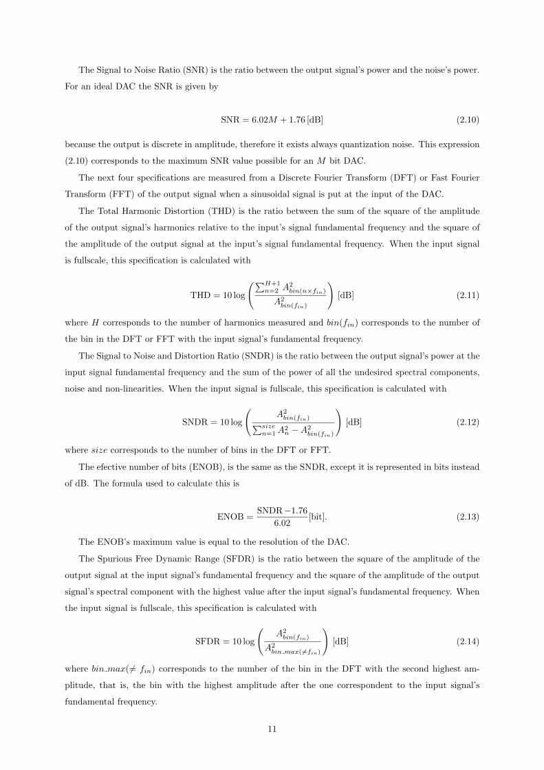
Glitches are undesired transitions in the output signal of the DAC. These transitions are generally
caused by the internal elements of the DAC that do not commute simultaneously. For instance, in Fig.2.9
9
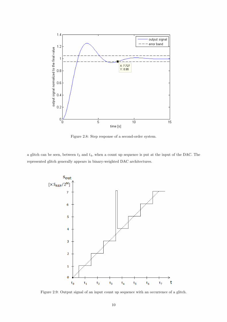
Figure 2.8: Step response of a second-order system.
a glitch can be seen, between t3 and t4, when a count up sequence is put at the input of the DAC. The
represented glitch generally appears in binary-weighted DAC architectures.
Figure 2.9: Output signal of an input count up sequence with an occurrence of a glitch.
10
The Signal to Noise Ratio (SNR) is the ratio between the output signal’s power and the noise’s power.
For an ideal DAC the SNR is given by
SNR = 6.02M + 1.76 [dB] (2.10)
because the output is discrete in amplitude, therefore it exists always quantization noise. This expression
(2.10) corresponds to the maximum SNR value possible for an M bit DAC.
The next four specifications are measured from a Discrete Fourier Transform (DFT) or Fast Fourier
Transform (FFT) of the output signal when a sinusoidal signal is put at the input of the DAC.
The Total Harmonic Distortion (THD) is the ratio between the sum of the square of the amplitude
of the output signal’s harmonics relative to the input’s signal fundamental frequency and the square of
the amplitude of the output signal at the input’s signal fundamental frequency. When the input signal
is fullscale, this specification is calculated with
THD = 10 log
(∑H+1n=2 A
2bin(n×fin)
A2bin(fin)
)[dB] (2.11)
where H corresponds to the number of harmonics measured and bin(fin) corresponds to the number of
the bin in the DFT or FFT with the input signal’s fundamental frequency.
The Signal to Noise and Distortion Ratio (SNDR) is the ratio between the output signal’s power at the
input signal fundamental frequency and the sum of the power of all the undesired spectral components,
noise and non-linearities. When the input signal is fullscale, this specification is calculated with
SNDR = 10 log
(A2bin(fin)∑size
n=1A2n −A2
bin(fin)
)[dB] (2.12)
where size corresponds to the number of bins in the DFT or FFT.
The efective number of bits (ENOB), is the same as the SNDR, except it is represented in bits instead
of dB. The formula used to calculate this is
ENOB =SNDR−1.76
6.02[bit]. (2.13)
The ENOB’s maximum value is equal to the resolution of the DAC.
The Spurious Free Dynamic Range (SFDR) is the ratio between the square of the amplitude of the
output signal at the input signal’s fundamental frequency and the square of the amplitude of the output
signal’s spectral component with the highest value after the input signal’s fundamental frequency. When
the input signal is fullscale, this specification is calculated with
SFDR = 10 log
(A2bin(fin)
A2bin max(6=fin)
)[dB] (2.14)
where bin max(6= fin) corresponds to the number of the bin in the DFT with the second highest am-
plitude, that is, the bin with the highest amplitude after the one correspondent to the input signal’s
fundamental frequency.
11
When the input signal is not fullscale
10log10
(Pfullscale
PS
)
is added to the specifications measured in dB, where Pfullscale is the power of the sampled signal fullscale
and PS is the power of the sampled signal used for the calculation of the specification.
2.1.4 Digital-to-Analog Converter Architectures
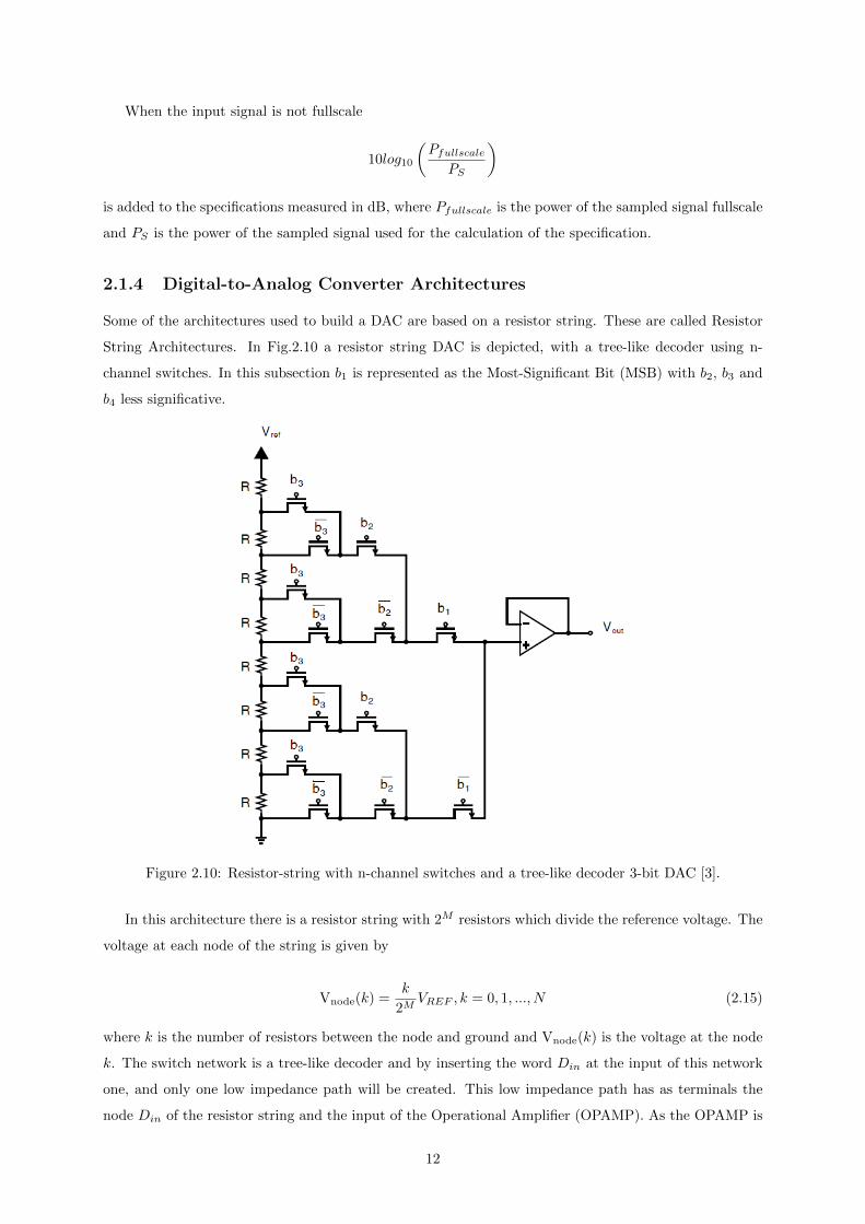
Some of the architectures used to build a DAC are based on a resistor string. These are called Resistor
String Architectures. In Fig.2.10 a resistor string DAC is depicted, with a tree-like decoder using n-
channel switches. In this subsection b1 is represented as the Most-Significant Bit (MSB) with b2, b3 and
b4 less significative.
Figure 2.10: Resistor-string with n-channel switches and a tree-like decoder 3-bit DAC [3].
In this architecture there is a resistor string with 2M resistors which divide the reference voltage. The
voltage at each node of the string is given by
Vnode(k) =k
2MVREF , k = 0, 1, ..., N (2.15)
where k is the number of resistors between the node and ground and Vnode(k) is the voltage at the node
k. The switch network is a tree-like decoder and by inserting the word Din at the input of this network
one, and only one low impedance path will be created. This low impedance path has as terminals the
node Din of the resistor string and the input of the Operational Amplifier (OPAMP). As the OPAMP is
12

setup like a buffer its output is equal to its input, which means the output voltage is given similarly to
(2.1).
In this architecture the number of resistors in the resistor string and transistors in the switch network
increase exponentially with the resolution of the DAC which cause problems of area for higher resolution.
Furthermore, the time constant of the low impedance path increases quadratically with the resolution of
the DAC, increasing significantly the settling time of the DAC. Due to this, these kind of DACs are more
advantageous for lower resolutions.
Other category of DAC architectures are Binary-Scaled Converters. In Fig.2.11 a Binary-Scaled
Converter with binary weighted resistors is shown.
Figure 2.11: Binary weighted resistors 4-bit DAC [3].
In this architecture there are M branches, one for each bit, each with a resistor in it. The resistance
of each of these resistors is proportional to the bit it represents, increasing exponentially from branch to
branch. In each branch there is also a switch, which is connected to ground or the OPAMP, depending
on the corresponding bit value. The OPAMP in the DAC is implemented as a weighted summer, so,
each branch that is connected to it adds an amount of current to the OPAMP proportional to the ratio
between the resistor on the branch and RF and is converted to voltage at RF . The output voltage of this
DAC is given by the expression
Vout =
M∑i=1
(bi ×
RF2i ×R
VREF
)(2.16)
which is proportional to the expressions (2.1) and (2.2) combined.
This architecture has only one resistor and switch per bit but for high resolution DACs the resistance
becomes large, as it increases exponencially (2i × R) with the resolution. This causes the area of the
DAC to increase exponentially with the resolution. Also, as all resistors have different resistances, this
architecture is very likely to have glitches and non-linearity issues.
A binary scaled architecture that solves some of the previous architecture problems is the R-2R
architecture, that changes the binary weighted resistors for a R-2R ladder. This ladder, which is presented
in Fig.2.12, has different current values in each branch that change with a power of 2 by 2 from branch
to branch with
13
Ii =VREF2i ×R
. (2.17)
Figure 2.12: R-2R ladder with 4 bits [3].
The architecture of the DAC with a R-2R ladder is presented in Fig. 2.13. Each branch that is
connected to the DAC adds a current Ii to the weighted summer resulting in an output voltage given by
Vout =
M∑i=1
(bi ×
Ii ×R2i−1
)(2.18)
resulting in an expression similar to (2.16) because I1 = IR = VREF
2R .
Figure 2.13: Binary-weighted R-2R DAC with 4 bits. [3].
This architecture does not present size issues for high resolutions because the resistance required for the
resistors are only R, 2R and RF . The linearity is also better because achieving smaller mismatch between
resistors of resistance R and 2R is easier than between 2R and 2i ×R, with 2 ≤ i ≤M . Nevertheless, as
the currents injected into the weighted summer are comparatively exponential, this architecture still has
glitches.
The most used DAC architecture in the telecommunication systems area is the Current-Steering DAC.
This architecture, used in this thesis, is composed of a current-source array with switches and a resistor,
which transform current to voltage. The array of current sources can be binary-weighted, as in Fig.2.14,
or thermometer coded. The binary weighted current-steering DAC works as the previous architectures
adding current to the DAC with each branch connected to it, and converting the current in the resistor to
voltage. The thermometer coded current-steering DAC, instead of having an array of M current sources
14
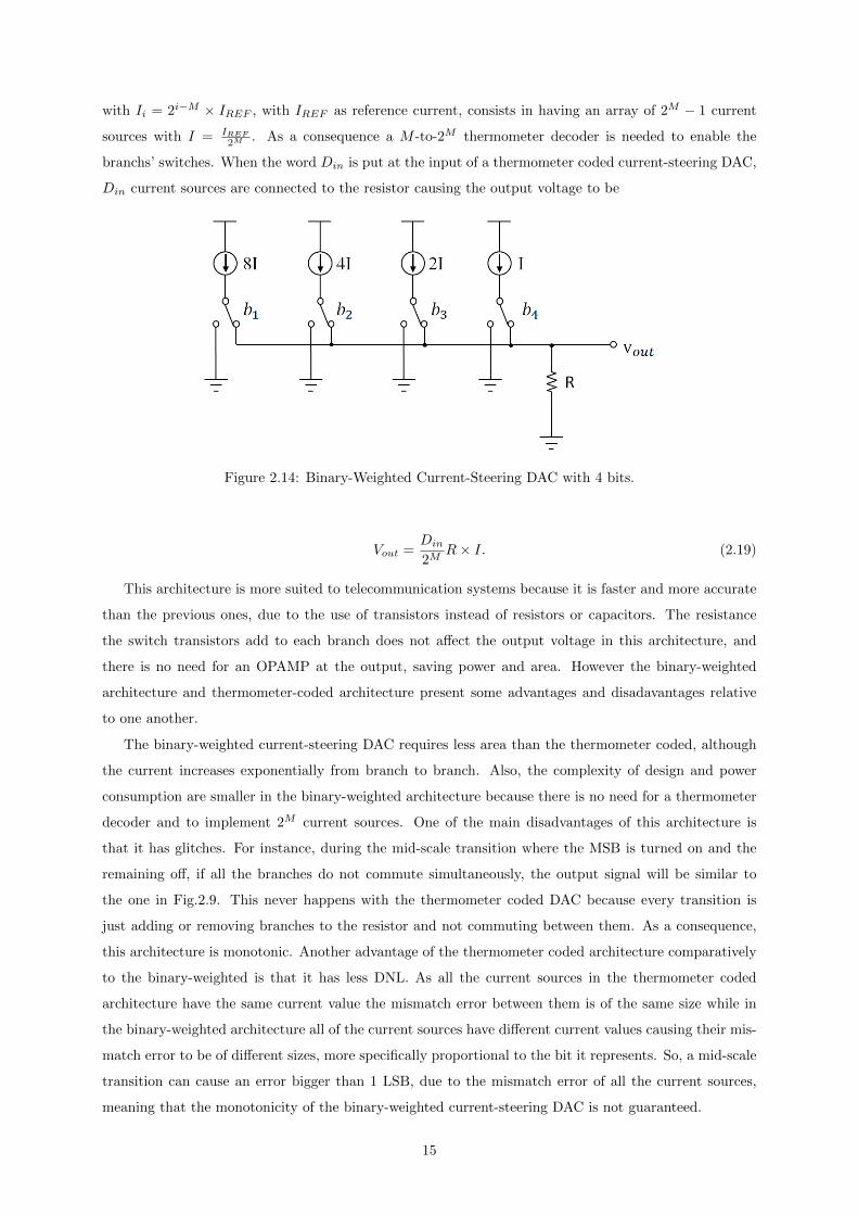
with Ii = 2i−M × IREF , with IREF as reference current, consists in having an array of 2M − 1 current
sources with I = IREF
2M . As a consequence a M -to-2M thermometer decoder is needed to enable the
branchs’ switches. When the word Din is put at the input of a thermometer coded current-steering DAC,
Din current sources are connected to the resistor causing the output voltage to be
Figure 2.14: Binary-Weighted Current-Steering DAC with 4 bits.
Vout =Din
2MR× I. (2.19)
This architecture is more suited to telecommunication systems because it is faster and more accurate
than the previous ones, due to the use of transistors instead of resistors or capacitors. The resistance
the switch transistors add to each branch does not affect the output voltage in this architecture, and
there is no need for an OPAMP at the output, saving power and area. However the binary-weighted
architecture and thermometer-coded architecture present some advantages and disadavantages relative
to one another.
The binary-weighted current-steering DAC requires less area than the thermometer coded, although
the current increases exponentially from branch to branch. Also, the complexity of design and power
consumption are smaller in the binary-weighted architecture because there is no need for a thermometer
decoder and to implement 2M current sources. One of the main disadvantages of this architecture is
that it has glitches. For instance, during the mid-scale transition where the MSB is turned on and the
remaining off, if all the branches do not commute simultaneously, the output signal will be similar to
the one in Fig.2.9. This never happens with the thermometer coded DAC because every transition is
just adding or removing branches to the resistor and not commuting between them. As a consequence,
this architecture is monotonic. Another advantage of the thermometer coded architecture comparatively
to the binary-weighted is that it has less DNL. As all the current sources in the thermometer coded
architecture have the same current value the mismatch error between them is of the same size while in
the binary-weighted architecture all of the current sources have different current values causing their mis-
match error to be of different sizes, more specifically proportional to the bit it represents. So, a mid-scale
transition can cause an error bigger than 1 LSB, due to the mismatch error of all the current sources,
meaning that the monotonicity of the binary-weighted current-steering DAC is not guaranteed.
15
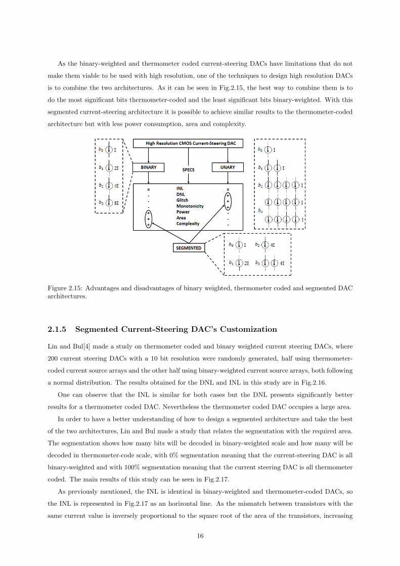
As the binary-weighted and thermometer coded current-steering DACs have limitations that do not
make them viable to be used with high resolution, one of the techniques to design high resolution DACs
is to combine the two architectures. As it can be seen in Fig.2.15, the best way to combine them is to
do the most significant bits thermometer-coded and the least significant bits binary-weighted. With this
segmented current-steering architecture it is possible to achieve similar results to the thermometer-coded
architecture but with less power consumption, area and complexity.
Figure 2.15: Advantages and disadvantages of binary weighted, thermometer coded and segmented DACarchitectures.
2.1.5 Segmented Current-Steering DAC’s Customization
Lin and Bul[4] made a study on thermometer coded and binary weighted current steering DACs, where
200 current steering DACs with a 10 bit resolution were randomly generated, half using thermometer-
coded current source arrays and the other half using binary-weighted current source arrays, both following
a normal distribution. The results obtained for the DNL and INL in this study are in Fig.2.16.
One can observe that the INL is similar for both cases but the DNL presents significantly better
results for a thermometer coded DAC. Nevertheless the thermometer coded DAC occupies a large area.
In order to have a better understanding of how to design a segmented architecture and take the best
of the two architectures, Lin and Bul made a study that relates the segmentation with the required area.
The segmentation shows how many bits will be decoded in binary-weighted scale and how many will be
decoded in thermometer-code scale, with 0% segmentation meaning that the current-steering DAC is all
binary-weighted and with 100% segmentation meaning that the current steering DAC is all thermometer
coded. The main results of this study can be seen in Fig.2.17.
As previously mentioned, the INL is identical in binary-weighted and thermometer-coded DACs, so
the INL is represented in Fig.2.17 as an horizontal line. As the mismatch between transistors with the
same current value is inversely proportional to the square root of the area of the transistors, increasing
16
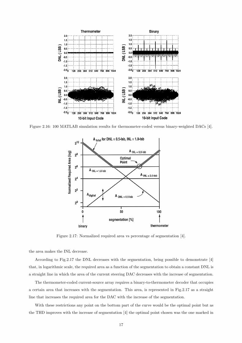
Figure 2.16: 100 MATLAB simulation results for thermometer-coded versus binary-weighted DACs [4].
Figure 2.17: Normalized required area vs percentage of segmentation [4].
the area makes the INL decrease.
According to Fig.2.17 the DNL decreases with the segmentation, being possible to demonstrate [4]
that, in logarithmic scale, the required area as a function of the segmentation to obtain a constant DNL is
a straight line in which the area of the current steering DAC decreases with the increase of segmentation.
The thermometer-coded current-source array requires a binary-to-thermometer decoder that occupies
a certain area that increases with the segmentation. This area, is represented in Fig.2.17 as a straight
line that increases the required area for the DAC with the increase of the segmentation.
With these restrictions any point on the bottom part of the curve would be the optimal point but as
the THD improves with the increase of segmentation [4] the optimal point chosen was the one marked in
17
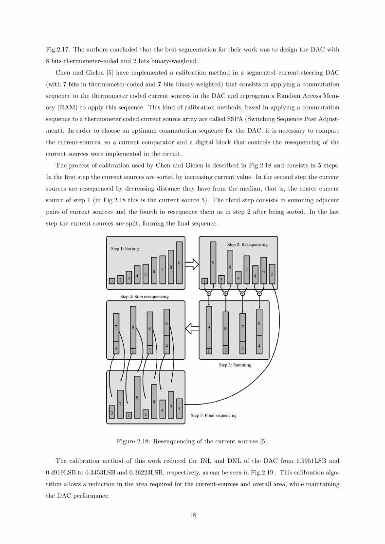
Fig.2.17. The authors concluded that the best segmentation for their work was to design the DAC with
8 bits thermometer-coded and 2 bits binary-weighted.
Chen and Gielen [5] have implemented a calibration method in a segmented current-steering DAC
(with 7 bits in thermometer-coded and 7 bits binary-weighted) that consists in applying a commutation
sequence to the thermometer coded current sources in the DAC and reprogram a Random Access Mem-
ory (RAM) to apply this sequence. This kind of calibration methods, based in applying a commutation
sequence to a thermometer coded current source array are called SSPA (Switching Sequence Post Adjust-
ment). In order to choose an optimum commutation sequence for the DAC, it is necessary to compare
the current-sources, so a current comparator and a digital block that controls the resequencing of the
current sources were implemented in the circuit.
The process of calibration used by Chen and Gielen is described in Fig.2.18 and consists in 5 steps.
In the first step the current sources are sorted by increasing current value. In the second step the current
sources are resequenced by decreasing distance they have from the median, that is, the center current
source of step 1 (in Fig.2.18 this is the current source 5). The third step consists in summing adjacent
pairs of current sources and the fourth in resequence them as in step 2 after being sorted. In the last
step the current sources are split, forming the final sequence.
Figure 2.18: Resenquencing of the current sources [5].
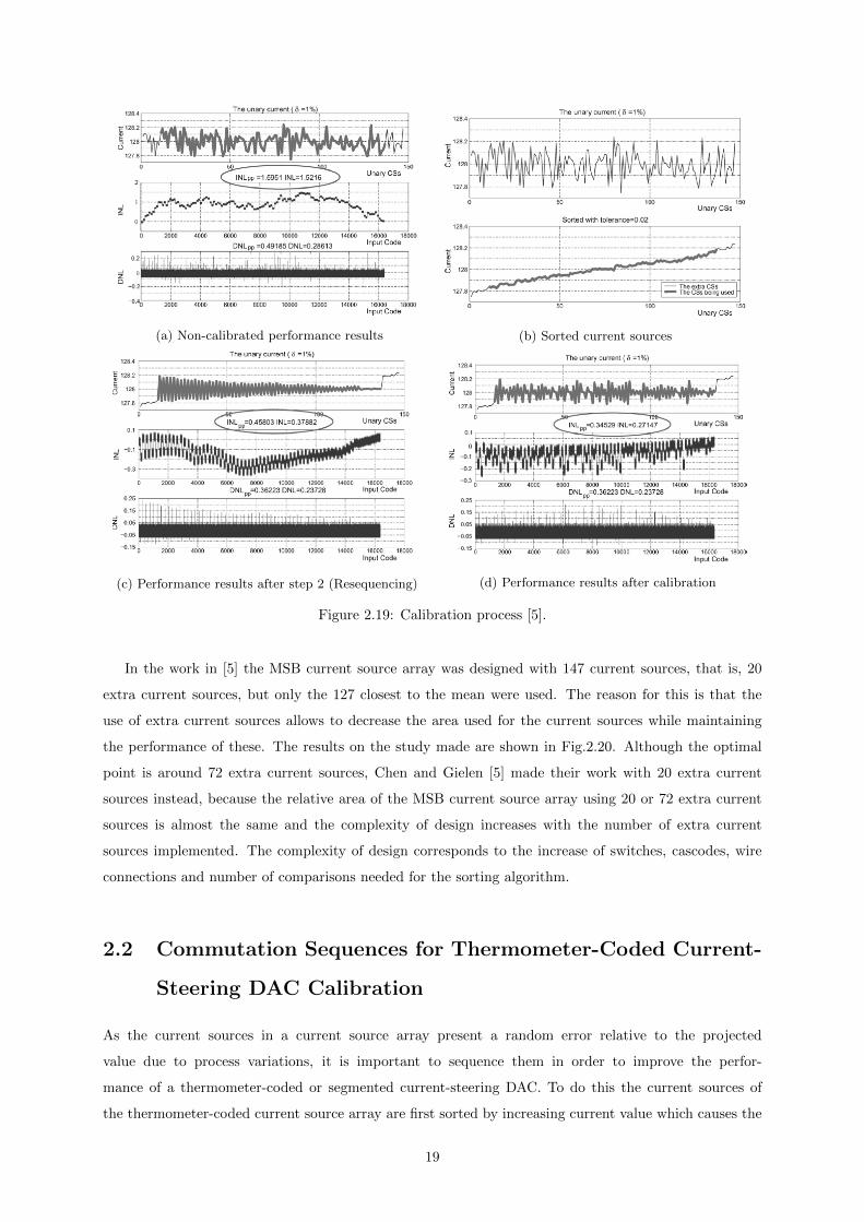
The calibration method of this work reduced the INL and DNL of the DAC from 1.5951LSB and
0.4919LSB to 0.3453LSB and 0.36223LSB, respectively, as can be seen in Fig.2.19 . This calibration algo-
rithm allows a reduction in the area required for the current-sources and overall area, while maintaining
the DAC performance.
18
(a) Non-calibrated performance results (b) Sorted current sources
(c) Performance results after step 2 (Resequencing) (d) Performance results after calibration
Figure 2.19: Calibration process [5].
In the work in [5] the MSB current source array was designed with 147 current sources, that is, 20
extra current sources, but only the 127 closest to the mean were used. The reason for this is that the
use of extra current sources allows to decrease the area used for the current sources while maintaining
the performance of these. The results on the study made are shown in Fig.2.20. Although the optimal
point is around 72 extra current sources, Chen and Gielen [5] made their work with 20 extra current
sources instead, because the relative area of the MSB current source array using 20 or 72 extra current
sources is almost the same and the complexity of design increases with the number of extra current
sources implemented. The complexity of design corresponds to the increase of switches, cascodes, wire
connections and number of comparisons needed for the sorting algorithm.
2.2 Commutation Sequences for Thermometer-Coded Current-
Steering DAC Calibration
As the current sources in a current source array present a random error relative to the projected
value due to process variations, it is important to sequence them in order to improve the perfor-
mance of a thermometer-coded or segmented current-steering DAC. To do this the current sources of
the thermometer-coded current source array are first sorted by increasing current value which causes the
19
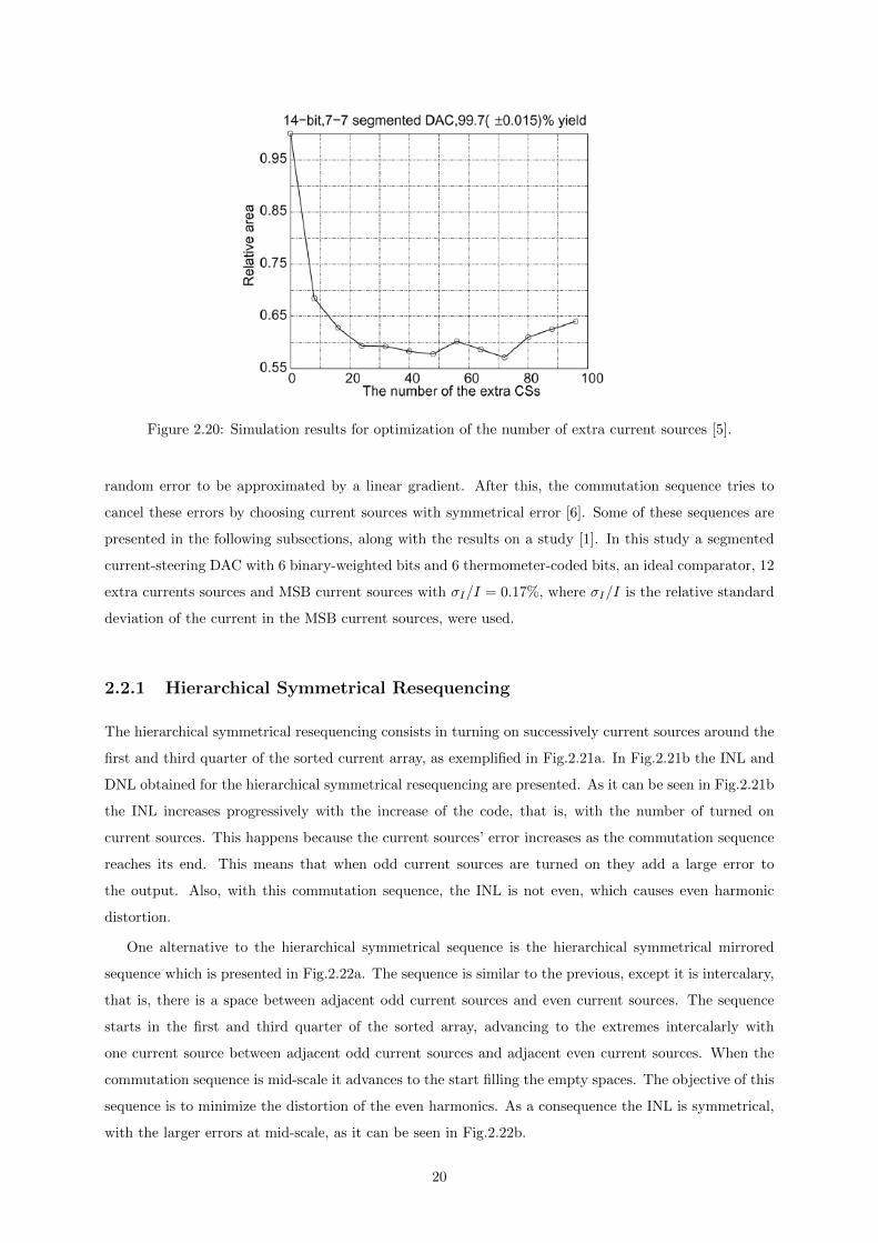
Figure 2.20: Simulation results for optimization of the number of extra current sources [5].
random error to be approximated by a linear gradient. After this, the commutation sequence tries to
cancel these errors by choosing current sources with symmetrical error [6]. Some of these sequences are
presented in the following subsections, along with the results on a study [1]. In this study a segmented
current-steering DAC with 6 binary-weighted bits and 6 thermometer-coded bits, an ideal comparator, 12
extra currents sources and MSB current sources with σI/I = 0.17%, where σI/I is the relative standard
deviation of the current in the MSB current sources, were used.
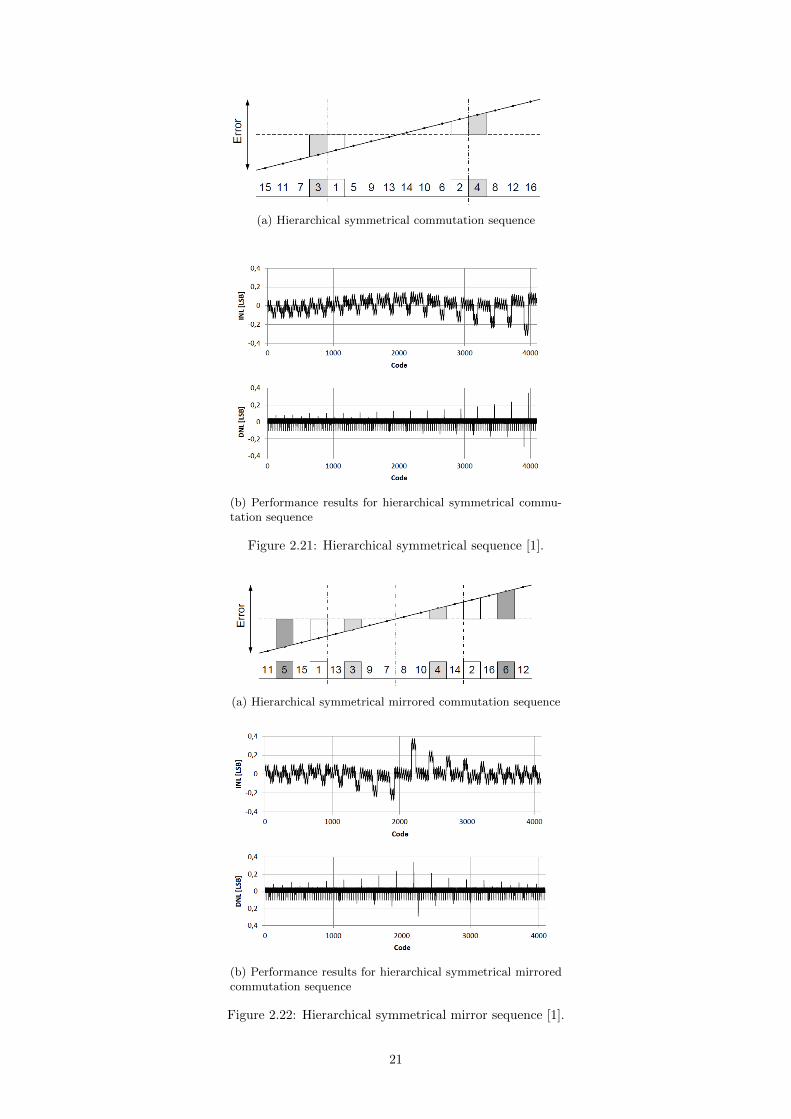
2.2.1 Hierarchical Symmetrical Resequencing
The hierarchical symmetrical resequencing consists in turning on successively current sources around the
first and third quarter of the sorted current array, as exemplified in Fig.2.21a. In Fig.2.21b the INL and
DNL obtained for the hierarchical symmetrical resequencing are presented. As it can be seen in Fig.2.21b
the INL increases progressively with the increase of the code, that is, with the number of turned on
current sources. This happens because the current sources’ error increases as the commutation sequence
reaches its end. This means that when odd current sources are turned on they add a large error to
the output. Also, with this commutation sequence, the INL is not even, which causes even harmonic
distortion.
One alternative to the hierarchical symmetrical sequence is the hierarchical symmetrical mirrored
sequence which is presented in Fig.2.22a. The sequence is similar to the previous, except it is intercalary,
that is, there is a space between adjacent odd current sources and even current sources. The sequence
starts in the first and third quarter of the sorted array, advancing to the extremes intercalarly with
one current source between adjacent odd current sources and adjacent even current sources. When the
commutation sequence is mid-scale it advances to the start filling the empty spaces. The objective of this
sequence is to minimize the distortion of the even harmonics. As a consequence the INL is symmetrical,
with the larger errors at mid-scale, as it can be seen in Fig.2.22b.
20
(a) Hierarchical symmetrical commutation sequence
(b) Performance results for hierarchical symmetrical commu-tation sequence
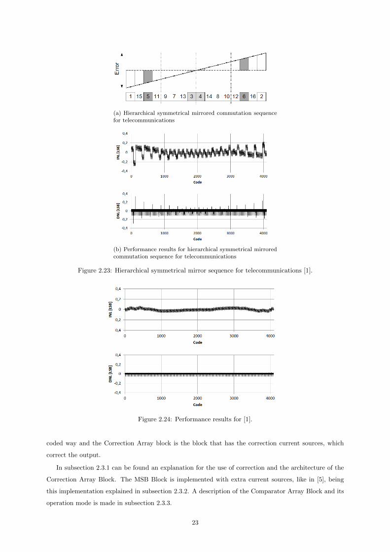
Figure 2.21: Hierarchical symmetrical sequence [1].
(a) Hierarchical symmetrical mirrored commutation sequence
(b) Performance results for hierarchical symmetrical mirroredcommutation sequence
Figure 2.22: Hierarchical symmetrical mirror sequence [1].
21

2.2.2 State-of-the-Art Resequencing
In telecommunication systems, modulations like Orthogonal Frequency Division Multiplexing (OFDM)
have a mean energy level significantly below full scale. As so, it is preferable to have the larger errors at
the extremes of the INL characteristic. One commutation sequence used to implement this characteristic
is the one in Fig.2.23a that is similar to the hierarchical symmetrical mirrored sequence, except that it
starts at the extremes and advances to the center intercalarly, returning afterwards. The maximum and
minimal INL values are similar to the results in subsection 2.2.1 as it can be seen in Fig.2.23b, although
the larger errors are now in the extremes of the INL characteristic. This commuting sequence has reduced
even harmonic distortion like the hierarchical symmetrical mirrored sequence as the INL characteristic is
even.
When choosing a commutation sequence it is advisable for it to be symmetrical, as this cancels the
INL error every pair of current sources enabled. If the error generated by enabled odd current sources
is not cancelled by the next current source enabled then increased deviation can occur, resulting in an
higher INL. To improve this effect a commutation sequence was used [1], similar to the latter presented,
with the difference that the current sources are grouped in pairs, and when only one of the current sources
of the pair has to be enabled, the current source is randomly selected between the two. For instance, if
the input of the DAC is Din = 1, only one of the current sources of the pair formed by the current sources
1 and 2 is enabled, being selected randomly one of the two. If Din = 2 the current sources 1 and 2 will
be enabled. This sequence, which is not deterministic, performs the mean of the error along the code,
decreasing the total error. As so, the INL and DNL characteristic are dynamic and depict the mean error
presented by the codes. The results obtained from this commutation sequence are in Fig.2.24. As it can
be seen this commutation sequence decreases the DNL and INL significantly, while maintaining the even
harmonic distortion small as the INL is even.
2.3 Specifications of the developed DAC
The specifications of the developed DAC are presented in this chapter, which include correction current
sources, extra MSB current sources and the comparator used.
The DAC presented in this work is a segmented current steering DAC with 12 bit resolution, in order
to compare to use [1] as a benchmark for comparison, using 6 bits thermometer coded and 6 bits binary
weighted, an output swing of 0.5 V, a supply voltage of 1.2 V and a resistor of 200Ω to convert the current
to voltage.
A block diagram of the DAC can be seen in Fig.2.25 where the interaction with the microprocessor
is present. The Control Unit block is a digital block that controls the operations of the DAC and
communicates with the microprocessor. The Decode/Memory is a writable digital block that stores
and decodes information from the control unit and controls the switches of the current sources. The
Decode/Memory and Control Unit are not studied in this thesis. The LSB array block corresponds to
the block with the LSB current sources, which are implemented in a binary-weighted way, the MSB array
block corresponds to the block with the MSB current sources, which are implemented in a thermometer-
22
(a) Hierarchical symmetrical mirrored commutation sequencefor telecommunications
(b) Performance results for hierarchical symmetrical mirroredcommutation sequence for telecommunications
Figure 2.23: Hierarchical symmetrical mirror sequence for telecommunications [1].
Figure 2.24: Performance results for [1].
coded way and the Correction Array block is the block that has the correction current sources, which
correct the output.
In subsection 2.3.1 can be found an explanation for the use of correction and the architecture of the
Correction Array Block. The MSB Block is implemented with extra current sources, like in [5], being
this implementation explained in subsection 2.3.2. A description of the Comparator Array Block and its
operation mode is made in subsection 2.3.3.
23
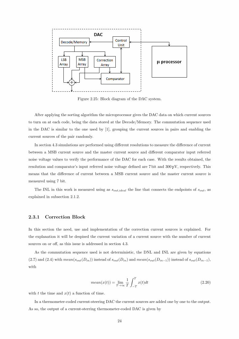
Figure 2.25: Block diagram of the DAC system.
After applying the sorting algorithm the microprocessor gives the DAC data on which current sources
to turn on at each code, being the data stored at the Decode/Memory. The commutation sequence used
in the DAC is similar to the one used by [1], grouping the current sources in pairs and enabling the
current sources of the pair randomly.
In section 4.3 simulations are performed using different resolutions to measure the difference of current
between a MSB current source and the master current source and different comparator input referred
noise voltage values to verify the performance of the DAC for each case. With the results obtained, the
resolution and comparator’s input referred noise voltage defined are 7 bit and 300µV, respectively. This
means that the difference of current between a MSB current source and the master current source is
measured using 7 bit.
The INL in this work is measured using as sout,ideal the line that connects the endpoints of sout, as
explained in subsection 2.1.2.
2.3.1 Correction Block
In this section the need, use and implementation of the correction current sources is explained. For
the explanation it will be despised the current variation of a current source with the number of current
sources on or off, as this issue is addressed in section 4.3.
As the commutation sequence used is not deterministic, the DNL and INL are given by equations
(2.7) and (2.4) with mean(sout(Din)) instead of sout(Din) and mean(sout(Din−1)) instead of sout(Din−1),
with
mean(x(t)) = limT→∞
1
T
∫ T
−Tx(t)dt (2.20)
with t the time and x(t) a function of time.
In a thermometer-coded current-steering DAC the current sources are added one by one to the output.
As so, the output of a current-sterring thermometer-coded DAC is given by
24
Iout(Din) =
Din∑k=1
Ik (2.21)
with Din the input word’s value and Ik the k current source of the current source array.
Using (2.7) and combining with (2.21) the DNL of the code Din of a current-steering thermometer-
coded DAC is given by
DNL(Din) =mean(IDin)−∆
∆. (2.22)
Assuming that the current source k of the current source array is affected of an error ek, due to process
variations, the current of that current source can be expressed as
Ik = ∆ + ek. (2.23)
In the DAC projected in this work the Dinth current source of an odd code Din is randomly selected
from a pair of current sources. Let IDin1and IDin2
be the current values of the pair of current sources
used for the Dinth current source. Considering that the choice of the current source is random with 50%
probability of each being selected and combining (2.22) and (2.23) it is obtained
DNL(Din) =eDin1
+ eDin2
2∆=ep∆
(2.24)
with ep the mean error of the pair p = round(Din
2 ) and round(x) the integer closer to the value x. In
case x has a fractional part of 0.5, round(x) is the integer closer to x with the largest value. In (2.24)
can be seen that DNL(Din) depends only on the mean error of the current sources in each pair.
Combining (2.7), (2.9) and (2.24) it is concluded that the DNL of a current-steering thermometer-
coded DAC with a commutation sequence similar to [1] is given by
DNLpair = max(∣∣∣ep
∆
∣∣∣) =∣∣∣ep max
∆
∣∣∣ (2.25)
where ep max represents the maximum absolute mean error of the pairs of current sources in the MSB
current source array. Notice that a commutation sequence with grouped pairs is better than a determinis-
tic for a current-steering DAC, as, combining (2.7), (2.9), (2.22) and (2.23), a deterministic commutation
sequence would have a
DNLsingle = max (DNL(Din)) = max(∣∣∣eDin
∆
∣∣∣) =∣∣∣emax
∆
∣∣∣ (2.26)
with emax the maximum absolute error of the current sources in the MSB current source array. Consid-
ering that the current source with error |emax| is grouped with other current source, then
DNLpair =
∣∣∣∣emax + erandom2∆
∣∣∣∣ ≤ ∣∣∣∣2emax2∆
∣∣∣∣ =∣∣∣emax
∆
∣∣∣ = DNLsingle . (2.27)
Nevertheless, the DAC presented in this work is segmented and not thermometer-coded. The thermometer-
25
coded current source array represents the MSBs and the binary-weighted current source array represents
the LSBs. The LSB current source array does not add a current to the output bigger than one of the
current sources in the MSB current source array. So, the biggest values for the DNL are obtained when
a MSB current source commutes in parallel with all the LSB current sources. This can be observed
in Fig.2.21b or Fig.2.22b, where the peaks correspond to the commutation of MSB current sources in
parallel with the LSB current sources and what is between the peaks to the commutation of LSB current
sources only. With this, the DNL of a segmented current-steering DAC using a grouped pair commutation
sequence is given by
DNL = max
(∣∣∣∣ep + eLSB∆
∣∣∣∣) =∣∣∣es max
∆
∣∣∣ (2.28)
with eLSB the sum of the error of all the binary-weighted current sources when they are toggled off and
with
es max = max(|ep + eLSB |). (2.29)
Therefore it is possible to conclude that the DNL of a segmented current-steering DAC with a grouped
pair commutation sequence is dependent of the error of the current sources inside a DAC and grouped pairs
of MSB current sources. Once the pairs are formed, the DNL value is independent of the commutation
sequence applied, as can be seen in expression (2.28) and in Fig.2.19c and Fig.2.19d, where only sequencing
occurs from one figure to the other.
Calculating max(| INL(Din)−INL(Din−1)|) in a segmented current-steering DAC using the definition
(2.4) and combining with (2.7), (2.9) and (2.28) the following is obtained
max(| INL(Din)− INL(Din − 1)|) = max(DNL(Din)) =∣∣∣es max
∆
∣∣∣ . (2.30)
Assuming that
| INL(Dmax)− INL(Dmax − 1)| =∣∣∣es max
∆
∣∣∣ (2.31)
with Dmax a value of Din that verifies the equation above, the minimum value that INL(Dmax) and
INL(Dmax − 1) can have in module is∣∣ es max
2∆
∣∣. This means that for a segmented current-steering DAC
INL ≥∣∣∣es max
2∆
∣∣∣ . (2.32)
In order to obtain smaller values for the INL it is needed to decrease the error of the current sources,
especially the MSB current sources, because these are the ones that contribute to es max the most. With
the use of correction current sources it is possible to decrease the σI
I used in the current sources of the
MSB current source array, which as a consequence decreases the area of the MSB current source array.
This method decreases the error of the MSB current sources, improving the DNL and INL.
This work proposes the use of a segmented current source array to measure the difference of current
26
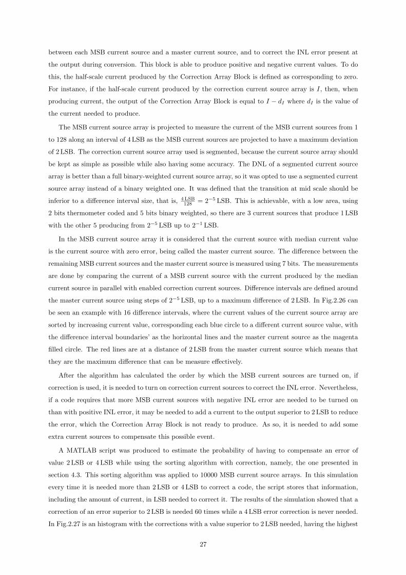
between each MSB current source and a master current source, and to correct the INL error present at
the output during conversion. This block is able to produce positive and negative current values. To do
this, the half-scale current produced by the Correction Array Block is defined as corresponding to zero.
For instance, if the half-scale current produced by the correction current source array is I, then, when
producing current, the output of the Correction Array Block is equal to I − dI where dI is the value of
the current needed to produce.
The MSB current source array is projected to measure the current of the MSB current sources from 1
to 128 along an interval of 4 LSB as the MSB current sources are projected to have a maximum deviation
of 2 LSB. The correction current source array used is segmented, because the current source array should
be kept as simple as possible while also having some accuracy. The DNL of a segmented current source
array is better than a full binary-weighted current source array, so it was opted to use a segmented current
source array instead of a binary weighted one. It was defined that the transition at mid scale should be
inferior to a difference interval size, that is, 4 LSB128 = 2−5 LSB. This is achievable, with a low area, using
2 bits thermometer coded and 5 bits binary weighted, so there are 3 current sources that produce 1 LSB
with the other 5 producing from 2−5 LSB up to 2−1 LSB.
In the MSB current source array it is considered that the current source with median current value
is the current source with zero error, being called the master current source. The difference between the
remaining MSB current sources and the master current source is measured using 7 bits. The measurements
are done by comparing the current of a MSB current source with the current produced by the median
current source in parallel with enabled correction current sources. Difference intervals are defined around
the master current source using steps of 2−5 LSB, up to a maximum difference of 2 LSB. In Fig.2.26 can
be seen an example with 16 difference intervals, where the current values of the current source array are
sorted by increasing current value, corresponding each blue circle to a different current source value, with
the difference interval boundaries’ as the horizontal lines and the master current source as the magenta
filled circle. The red lines are at a distance of 2 LSB from the master current source which means that
they are the maximum difference that can be measure effectively.
After the algorithm has calculated the order by which the MSB current sources are turned on, if
correction is used, it is needed to turn on correction current sources to correct the INL error. Nevertheless,
if a code requires that more MSB current sources with negative INL error are needed to be turned on
than with positive INL error, it may be needed to add a current to the output superior to 2 LSB to reduce
the error, which the Correction Array Block is not ready to produce. As so, it is needed to add some
extra current sources to compensate this possible event.
A MATLAB script was produced to estimate the probability of having to compensate an error of
value 2 LSB or 4 LSB while using the sorting algorithm with correction, namely, the one presented in
section 4.3. This sorting algorithm was applied to 10000 MSB current source arrays. In this simulation
every time it is needed more than 2 LSB or 4 LSB to correct a code, the script stores that information,
including the amount of current, in LSB needed to correct it. The results of the simulation showed that a
correction of an error superior to 2 LSB is needed 60 times while a 4 LSB error correction is never needed.
In Fig.2.27 is an histogram with the corrections with a value superior to 2 LSB needed, having the highest
27
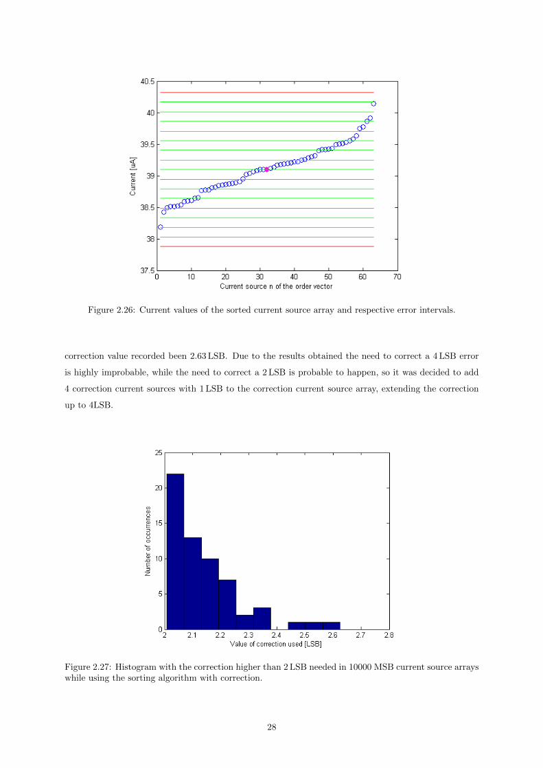
Figure 2.26: Current values of the sorted current source array and respective error intervals.
correction value recorded been 2.63 LSB. Due to the results obtained the need to correct a 4 LSB error
is highly improbable, while the need to correct a 2 LSB is probable to happen, so it was decided to add
4 correction current sources with 1 LSB to the correction current source array, extending the correction
up to 4LSB.
Figure 2.27: Histogram with the correction higher than 2 LSB needed in 10000 MSB current source arrayswhile using the sorting algorithm with correction.
28
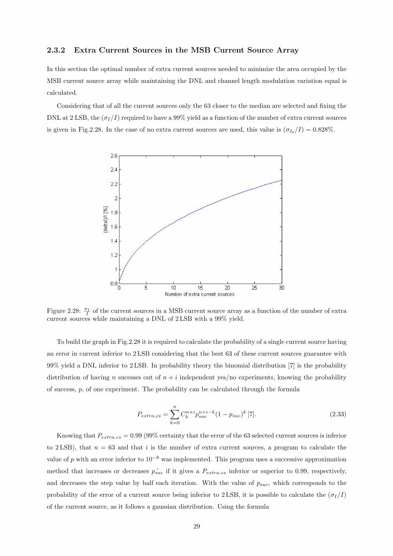
2.3.2 Extra Current Sources in the MSB Current Source Array
In this section the optimal number of extra current sources needed to minimize the area occupied by the
MSB current source array while maintaining the DNL and channel length modulation variation equal is
calculated.
Considering that of all the current sources only the 63 closer to the median are selected and fixing the
DNL at 2 LSB, the (σI/I) required to have a 99% yield as a function of the number of extra current sources
is given in Fig.2.28. In the case of no extra current sources are used, this value is (σI0/I) = 0.828%.
Figure 2.28: σI
I of the current sources in a MSB current source array as a function of the number of extracurrent sources while maintaining a DNL of 2 LSB with a 99% yield.
To build the graph in Fig.2.28 it is required to calculate the probability of a single current source having
an error in current inferior to 2 LSB considering that the best 63 of these current sources guarantee with
99% yield a DNL inferior to 2 LSB. In probability theory the binomial distribution [7] is the probability
distribution of having n sucesses out of n + i independent yes/no experiments, knowing the probability
of success, p, of one experiment. The probability can be calculated through the formula
Pextra cs =
n∑k=0
Cn+ik pn+i−k
suc (1− psuc)k [7]. (2.33)
Knowing that Pextra cs = 0.99 (99% certainty that the error of the 63 selected current sources is inferior
to 2 LSB), that n = 63 and that i is the number of extra current sources, a program to calculate the
value of p with an error inferior to 10−8 was implemented. This program uses a successive approximation
method that increases or decreases ˜psuc if it gives a Pextra cs inferior or superior to 0.99, respectively,
and decreases the step value by half each iteration. With the value of psuc, which corresponds to the
probability of the error of a current source being inferior to 2 LSB, it is possible to calculate the (σI/I)
of the current source, as it follows a gaussian distribution. Using the formula
29
(σI/I) = − 2−5
√2× erf−1(−psuc)
× 100 (2.34)
with
erf(x) =2√π
∫ x
0
e−t2
dt (2.35)
and erf−1(x) the inverse function of erf(x) and combining with the program implemented that estimates
p it is possible to obtain (σI/I) [%] in function of the number of extra current sources as can be seen in
Fig.2.28.
In order to compare between the area occupied with and without extra current sources the areas
A1 and A0, respectively, are defined. The first area has current sources with σI1/I and the second has
current sources with σI0/I. The results of Fig.2.28 are used in this comparison to define the σI1/I as a
function of the number of extra current sources. The relation between areas, taking only the area of the
current source transistors of the MSB current sources into account is given by
A1
A0=
(σI0σI1
)263 + nextra
63(2.36)
with nextra the number of extra current sources.
Nevertheless, the total area reduction can only be calculated using the other transistors within the
MSB current source, as only the current source transistor changes size with σI1 . The total area of a MSB
current source is then given by
Aun = APM1 ×(σI0σI1
)2
+Are (2.37)
where APM1 is the area of the designed current source transistor of the MSB current source for A0 and
Are is the area of the remaining transistors of the correspondent MSB current source. Using this, the
relative area as a function of the number of extra current sources guaranting a DNL inferior to 2 LSB
with 99% yield is given by
A1
A0=
(63 + nextra)× (APM1 ×(σI0
σI1
)2
+Are)
63× (APM1 +Are). (2.38)
To illustrate (2.38) real values are used for APM1 and Are, which will later be obtained in section
3.1, leading to the plot in Fig.2.29. From the results it was calculated that the number of extra current
sources to add to the current source array is 12 and to increase the σI/I of the current sources to 1.741%,
which reduces the area by 42.87%.
Nevertheless, the output impedance of the MSB current source changes with the variation of σI/I,
which is one of the main specifications for the MSB current source. In order to maintain the output
impedance equal (15.02 MΩ), Are has to change with the variation of σI1/I. As Are increases with the
increase of σI1/I, the number of extra current sources that minimizes the overall area is inferior or equal
to 12. In order to have the most reliable results a transistor level simulator was used to obtain the
30
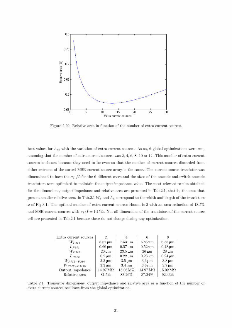
Figure 2.29: Relative area in function of the number of extra current sources.
best values for Are with the variation of extra current sources. As so, 6 global optimizations were run,
assuming that the number of extra current sources was 2, 4, 6, 8, 10 or 12. This number of extra current
sources is chosen because they need to be even so that the number of current sources discarded from
either extreme of the sorted MSB current source array is the same. The current source transistor was
dimensioned to have the σI1/I for the 6 different cases and the sizes of the cascode and switch cascode
transistors were optimized to maintain the output impedance value. The most relevant results obtained
for the dimensions, output impedance and relative area are presented in Tab.2.1, that is, the ones that
present smaller relative area. In Tab.2.1 Wx and Lx correspond to the width and length of the transistors
x of Fig.3.1. The optimal number of extra current sources chosen is 2 with an area reduction of 18.5%
and MSB current sources with σI/I = 1.15%. Not all dimensions of the transistors of the current source
cell are presented in Tab.2.1 because these do not change during any optimization.
Extra current sources 2 4 6 8WPM1 8.67 µm 7.53 µm 6.85 µm 6.38 µmLPM1 0.66 µm 0.57 µm 0.52 µm 0.48 µmWPM2 20 µm 23.5µm 26 µm 28 µmLPM2 0.2µm 0.22 µm 0.23 µm 0.24 µm
WPM3−PM6 3.3µm 3.5 µm 3.6µm 3.8 µmWPM7−PM10 3.3µm 3.4 µm 3.6µm 3.7 µm
Output impedance 14.97 MΩ 15.06 MΩ 14.97 MΩ 15.02 MΩRelative area 81.5% 83.26% 87.24% 92.43%
Table 2.1: Transistor dimensions, output impedance and relative area as a function of the number ofextra current sources resultant from the global optimization.
31
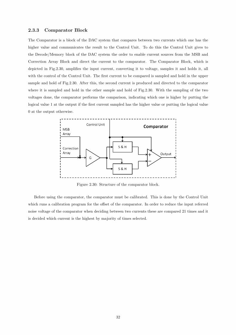
2.3.3 Comparator Block
The Comparator is a block of the DAC system that compares between two currents which one has the
higher value and communicates the result to the Control Unit. To do this the Control Unit gives to
the Decode/Memory block of the DAC system the order to enable current sources from the MSB and
Correction Array Block and direct the current to the comparator. The Comparator Block, which is
depicted in Fig.2.30, amplifies the input current, converting it to voltage, samples it and holds it, all
with the control of the Control Unit. The first current to be compared is sampled and hold in the upper
sample and hold of Fig.2.30. After this, the second current is produced and directed to the comparator
where it is sampled and hold in the other sample and hold of Fig.2.30. With the sampling of the two
voltages done, the comparator performs the comparison, indicating which one is higher by putting the
logical value 1 at the output if the first current sampled has the higher value or putting the logical value
0 at the output otherwise.
Figure 2.30: Structure of the comparator block.
Before using the comparator, the comparator must be calibrated. This is done by the Control Unit
which runs a calibration program for the offset of the comparator. In order to reduce the input referred
noise voltage of the comparator when deciding between two currents these are compared 21 times and it
is decided which current is the highest by majority of times selected.
32
Chapter 3
Analog Circuits
In this chapter the design and dimensioning of the MSB current source array and comparator are ex-
plained. In section 3.1 the design and dimensioning of the current sources of the MSB current source
array are presented. A simulated characteristic of a MSB current source at transistor level is also shown.
In section 3.2 the design and dimensioning of the comparator is presented.
3.1 MSB Current Source Array
The current source design used in the MSB current source array is the one in Fig.3.1. This current source
is composed by PM1, the current source transistor, PM2, the cascode transistor, PM3, PM4, PM5 and
PM6, the switch transistors, PM7, PM8, PM9 and PM10, the switch cascode transistors and I1 and I2,
two auxiliary current sources. The transistors used are PMOS instead of NMOS as the NMOS bulk’s
voltage must be equal to the substrate, if a triple well technology is not used, while the PMOS bulk’s
voltage can be equal to the source. This turns 3 of the transistors of a NMOS current source susceptible
to body effect, while that does not exist with a PMOS current source.
Four branches were designed for the current source cell, one branch to connect to the comparator, one
branch to generate the output, and two to serve as dummies. Only one branch is enabled every time, so
when a disabled branch is enabled, the one that was previously enabled is disabled. The dummy branches
are needed in the design to ensure fast commutations, as it is faster to commute the current from one
branch to another than to turn the current on and off.
The reference current of the DAC is I =Vout swing
Rout= 0.5
200 = 2.5 mA. As 6 of the 12 bits of the DAC
are thermometer coded each MSB current source designed generates a current IMSB = I26 = 39.0625 µA.
From the simulation that generated Fig.2.28 in subsection 2.3.2 it is seen that for a DNL of 2 LSB to be
achieved with 99% yield for the MSB current source array with no extra current sources, these have to
be designed with (σI0/I) = 0.828%.
Pelgrom [8] demonstrated that the standard deviation, σI , of the current, I, that is generated in a
transistor with width W and length L is given by
33
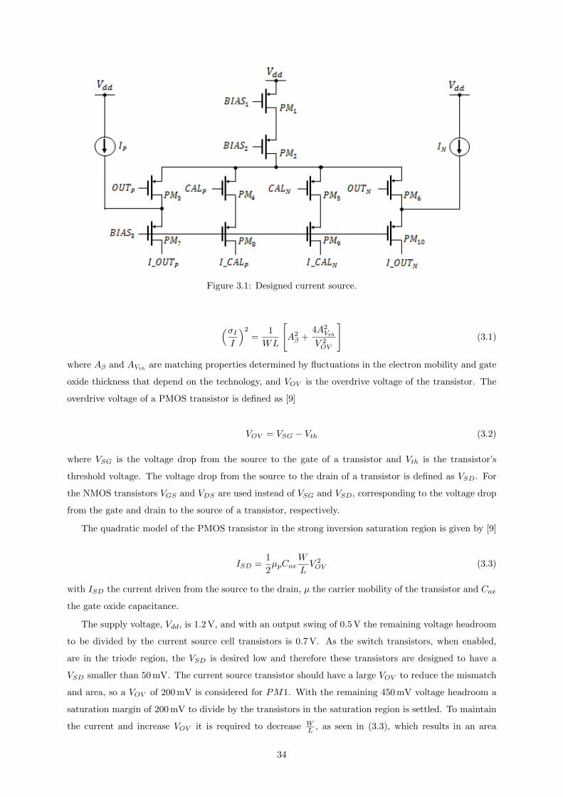
Figure 3.1: Designed current source.
(σII
)2
=1
WL
[A2β +
4A2Vth
V 2OV
](3.1)
where Aβ and AVthare matching properties determined by fluctuations in the electron mobility and gate
oxide thickness that depend on the technology, and VOV is the overdrive voltage of the transistor. The
overdrive voltage of a PMOS transistor is defined as [9]
VOV = VSG − Vth (3.2)
where VSG is the voltage drop from the source to the gate of a transistor and Vth is the transistor’s
threshold voltage. The voltage drop from the source to the drain of a transistor is defined as VSD. For
the NMOS transistors VGS and VDS are used instead of VSG and VSD, corresponding to the voltage drop
from the gate and drain to the source of a transistor, respectively.
The quadratic model of the PMOS transistor in the strong inversion saturation region is given by [9]
ISD =1
2µpCox
W
LV 2OV (3.3)
with ISD the current driven from the source to the drain, µ the carrier mobility of the transistor and Cox
the gate oxide capacitance.
The supply voltage, Vdd, is 1.2 V, and with an output swing of 0.5 V the remaining voltage headroom
to be divided by the current source cell transistors is 0.7 V. As the switch transistors, when enabled,
are in the triode region, the VSD is desired low and therefore these transistors are designed to have a
VSD smaller than 50 mV. The current source transistor should have a large VOV to reduce the mismatch
and area, so a VOV of 200 mV is considered for PM1. With the remaining 450 mV voltage headroom a
saturation margin of 200 mV to divide by the transistors in the saturation region is settled. To maintain
the current and increase VOV it is required to decrease WL , as seen in (3.3), which results in an area
34
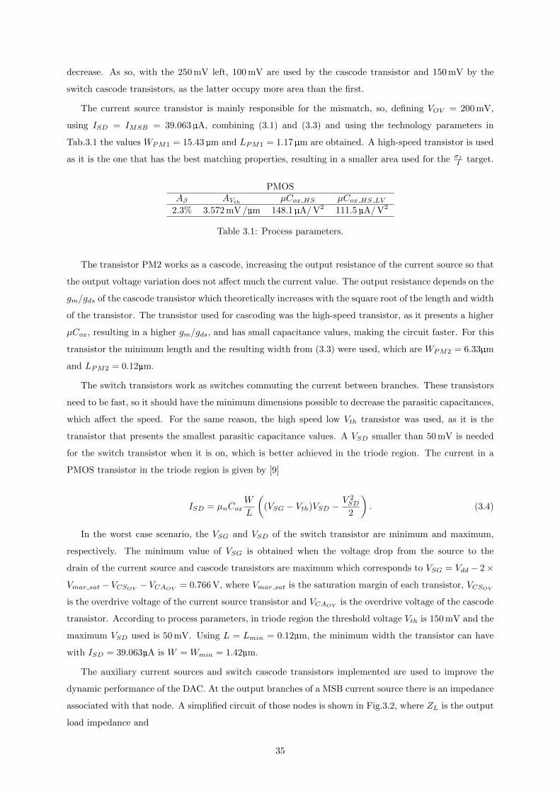
decrease. As so, with the 250 mV left, 100 mV are used by the cascode transistor and 150 mV by the
switch cascode transistors, as the latter occupy more area than the first.
The current source transistor is mainly responsible for the mismatch, so, defining VOV = 200 mV,
using ISD = IMSB = 39.063 µA, combining (3.1) and (3.3) and using the technology parameters in
Tab.3.1 the values WPM1 = 15.43 µm and LPM1 = 1.17 µm are obtained. A high-speed transistor is used
as it is the one that has the best matching properties, resulting in a smaller area used for the σI
I target.
PMOSAβ AVth
µCox HS µCox HS LV
2.3% 3.572 mV /µm 148.1 µA/V2 111.5µA/V2
Table 3.1: Process parameters.
The transistor PM2 works as a cascode, increasing the output resistance of the current source so that
the output voltage variation does not affect much the current value. The output resistance depends on the
gm/gds of the cascode transistor which theoretically increases with the square root of the length and width
of the transistor. The transistor used for cascoding was the high-speed transistor, as it presents a higher
µCox, resulting in a higher gm/gds, and has small capacitance values, making the circuit faster. For this
transistor the minimum length and the resulting width from (3.3) were used, which are WPM2 = 6.33µm
and LPM2 = 0.12µm.
The switch transistors work as switches commuting the current between branches. These transistors
need to be fast, so it should have the minimum dimensions possible to decrease the parasitic capacitances,
which affect the speed. For the same reason, the high speed low Vth transistor was used, as it is the
transistor that presents the smallest parasitic capacitance values. A VSD smaller than 50 mV is needed
for the switch transistor when it is on, which is better achieved in the triode region. The current in a
PMOS transistor in the triode region is given by [9]
ISD = µnCoxW
L
((VSG − Vth)VSD −
V 2SD
2
). (3.4)
In the worst case scenario, the VSG and VSD of the switch transistor are minimum and maximum,
respectively. The minimum value of VSG is obtained when the voltage drop from the source to the
drain of the current source and cascode transistors are maximum which corresponds to VSG = Vdd − 2×
Vmar sat − VCSOV− VCAOV
= 0.766 V, where Vmar sat is the saturation margin of each transistor, VCSOV
is the overdrive voltage of the current source transistor and VCAOVis the overdrive voltage of the cascode
transistor. According to process parameters, in triode region the threshold voltage Vth is 150 mV and the
maximum VSD used is 50 mV. Using L = Lmin = 0.12µm, the minimum width the transistor can have
with ISD = 39.063µA is W = Wmin = 1.42µm.
The auxiliary current sources and switch cascode transistors implemented are used to improve the
dynamic performance of the DAC. At the output branches of a MSB current source there is an impedance
associated with that node. A simplified circuit of those nodes is shown in Fig.3.2, where ZL is the output
load impedance and
35

1
ZO=
ncs∑k=1
1
ZOk
, (3.5)
IO = IMSB × nO, (3.6)
1
ZD=
ncs∑k=1
1
ZDk
, (3.7)
ID = IMSB × nD (3.8)
with ZOkthe output impedance of the k MSB current source connected to the output node load, ZDk
the output impedance of the k MSB current source connected to the dummy node load, nO the number
of current sources connected to the output load and nD the number of current sources connected to the
dummy load.
Figure 3.2: DAC simplified output impedance equivalent circuit [10].
It is desirable that ZO does not change during conversion to maintain the output voltage linear,
but without the auxiliary current sources and switch cascode transistors this does not happen, causing
distortion in the output signal. This is due to the fact that the source to gate capacitance, CSG, of
the transistor connected to the load controls the frequency of the dominant pole of a current source’s
impedance [11] and is approximately constant in saturation region but has a significantly different value in
weak inversion. If the switch cascode transistors and auxiliary current sources were not used, when a MSB
current source commuted, the CSG of the transistor connected to the load would change significantly,
causing ZO to change and distortion would be introduced in the output. With the auxiliary current
sources and switch cascode transistor, when a MSB current source commutes, as the switch cascode
transistor continues in strong inversion, the output capacitance does not change significantly, improving
the dynamic performance of the DAC. A current correspondent to 1%− 2% of IMSB is enough to reduce
the distortion[12], so a 2% current was chosen, to reduce the effect as much as possible. This auxiliary
current increases the output voltage by 10 mV. In order to obtain the highest frequency possible for the
36
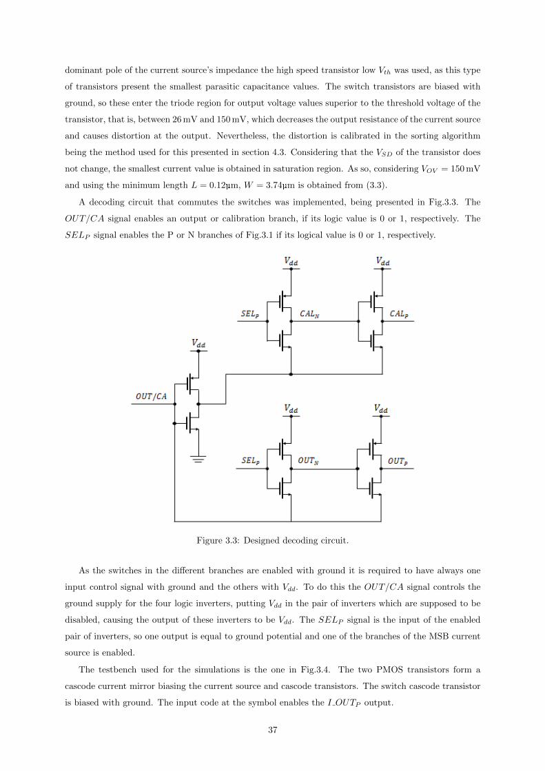
dominant pole of the current source’s impedance the high speed transistor low Vth was used, as this type
of transistors present the smallest parasitic capacitance values. The switch transistors are biased with
ground, so these enter the triode region for output voltage values superior to the threshold voltage of the
transistor, that is, between 26 mV and 150 mV, which decreases the output resistance of the current source
and causes distortion at the output. Nevertheless, the distortion is calibrated in the sorting algorithm
being the method used for this presented in section 4.3. Considering that the VSD of the transistor does
not change, the smallest current value is obtained in saturation region. As so, considering VOV = 150 mV
and using the minimum length L = 0.12µm, W = 3.74µm is obtained from (3.3).
A decoding circuit that commutes the switches was implemented, being presented in Fig.3.3. The
OUT/CA signal enables an output or calibration branch, if its logic value is 0 or 1, respectively. The
SELP signal enables the P or N branches of Fig.3.1 if its logical value is 0 or 1, respectively.
Figure 3.3: Designed decoding circuit.
As the switches in the different branches are enabled with ground it is required to have always one
input control signal with ground and the others with Vdd. To do this the OUT/CA signal controls the
ground supply for the four logic inverters, putting Vdd in the pair of inverters which are supposed to be
disabled, causing the output of these inverters to be Vdd. The SELP signal is the input of the enabled
pair of inverters, so one output is equal to ground potential and one of the branches of the MSB current
source is enabled.
The testbench used for the simulations is the one in Fig.3.4. The two PMOS transistors form a
cascode current mirror biasing the current source and cascode transistors. The switch cascode transistor
is biased with ground. The input code at the symbol enables the I OUTP output.
37
Figure 3.4: Testbench circuit used for the simulations.
DC monte carlo analysis was performed (500 runs), sweeping VTEST ’s voltage from 10 mV to 510 mV.
Based on the results from these simulations the dimensions of the transistors were tuned until (σI/I) ≤
1.15%, VSDswitch≤ 50 mV and INL < 2 LSB (considering there are no process variations) were obtained.
The latter requirement is due to the finite output impedance of the MSB current sources. After tuning,
the dimensions obtained are presented in Tab.3.2.
Transistor Width(µm) Length(µm)Current source 12.05 0.91
Cascode 14 0.18Switch 3 0.12
Thick oxide 2.9 0.12
Table 3.2: Dimensions of the transistors of the MSB current source cell.
As stated in subsection 2.3.2, 2 extra current sources were added to the MSB current source array,
decreasing the area of the MSB current source array and changing the dimensions to the ones in Tab.3.3.
With these MSB current source dimensions, 500 monte carlo simulations and a nominal simulation of
the output current as a function of the output voltage are presented in Fig.3.5 and Fig.3.6 respectively.
In Fig.3.5 i low corresponds to the current value when the output voltage is 10 mV, i high corresponds
to the current value when the output voltage is 510 mV, i var to the difference of the latter two and
vds spec to the VDS of the switch transistor of the enabled branch.
The (σI/I) target is achieved, as can be seen in Fig.3.5, with (σI/I) = 1.1% for i high and i low.
With i var = 33.4 nA the INL obtained considering that the MSB current sources do not suffer process
variations is around 1.8 LSB, which means that to achieve INL > 2 LSB, i var must be superior to 37.1 nA,
38

Transistor Width(µm) Length(µm)Current source 8.67 0.66
Cascode 20 0.2Switch 3.3 0.12
Thick oxide 3.3 0.12
Table 3.3: Dimensions of the transistors of the MSB current source cell after adding the extra currentsources.
Figure 3.5: Result of the 500 monte carlo simulations.
Figure 3.6: Output current produced by the current source cell as a function of the output voltage.
which is nearly 3.7 nA more than the mean value obtained in the simulation. The current values of the
MSB current sources are identical independent random variables with a gaussian distribution. According
to [7] the standard deviation and mean of the sum of n identical independent random variables with a
gaussian distribution is equal to
σ(X) =√nσ(Xi) (3.9)
µ(X) = nµ(Xi) (3.10)
where X =∑ni=1Xi and Xi, i = 1, ..., n are identical independent random variables with a gaussian
distribution. This means that combining (3.9) and (3.10)
σ(X)
µ(X)=
1√n
σ(Xi)
µ(Xi)(3.11)
With this, the 4 nA sigma value obtained in the simulation becomes insignificant as the relation σ/µ
of the output current decreases as more MSB current sources drive current to the output. The VSD target
39
for the switch transistor is achieved with a 96% yield, which is enough for the work, as this specification
is not the most relevant.
The area occupied by this current source array, without the interconnections, is 837.9 µm2.
3.2 Comparator Block
In this section the circuits belonging to the Comparator block are presented in three subsections, the
first, explaining the comparator of Fig.2.30, the second, explaining the amplifier and sample and holds in
Fig.2.30 and the third, explaining the circuit for the calibration of the offset voltage of the comparator.
The comparator is expected to have a 300µV input referred noise and a 50 µV maximum input offset,
with the lowest area possible. The sample & hold circuit combined with the amplifier add noise to the
comparator, so, the 300 µV are divided by the two, producing the sample & hold circuit a noise voltage
of 212 µV and having the comparator an input referred noise voltage of 212µV. This is possible as it is
the noise power that sums and not the noise voltage [9], which means
v2n3
= v2n2
+ v2n1
(3.12)
where v2n1
and v2n2
are two root mean square noise voltages produced by two independent different sources
and v2n3
is the resultant root mean square noise voltage from the sum of the two sources.
3.2.1 Architecure
The architecture of the comparator used in this work is based on the one presented in [13], with the
difference that the circuit is built with and for a PMOS differential input pair and capacitors are added
in the second stage, as can be seen in Fig.3.7.
The first stage of the comparator is in the upper part of Fig.3.7, having as inputs VIP and VIN , and
the second stage is in the lower part of Fig.3.7, having as outputs VOP and VON . The comparator is
controlled by the latch signal, performing a comparison when this signal is put at ground potential. In
Fig.3.8 the operation of the comparator can be seen, being explained in the following paragraphs.
Before a comparison is started the signal latch is at Vdd potential, which means that the transistor
M1 is off and M3P , M3N , M4P and M4N are on. This means that no current is being spent by the
comparator as M1 can be approximated by an open circuit, VCP and VCN are at ground potential, as
M3P and M3N are on, and M6P and M6N are off. The transistors M4P and M4N are on, which means
that VOP and VON begin the comparison at Vdd potential. Due to the latter M7P and M7N are on, so
the drain of these transistors start the comparison with ground potential.
The moment latch is toggled off M1 becomes on and M3P , M3N , M4P and M4N become off. The
transistor M1 starts to drive current, which passes through M2P and M2N and is integrated in C1P and
C1N as M3P and M3N are off. Considering that VIP > VIN the transistor M2N drives more current than
M2P , increasing VCN faster than VCP . Nevertheless VCN and VCP have a value very close one to another
as can be seen in Fig.3.8, where they seem overlapped. When VCN and VCP pass the threshold voltage
40
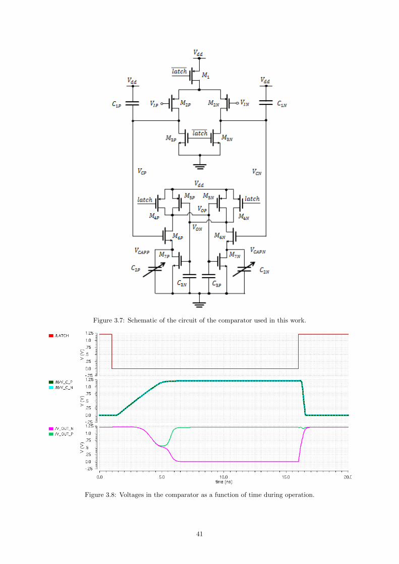
Figure 3.7: Schematic of the circuit of the comparator used in this work.
Figure 3.8: Voltages in the comparator as a function of time during operation.
41
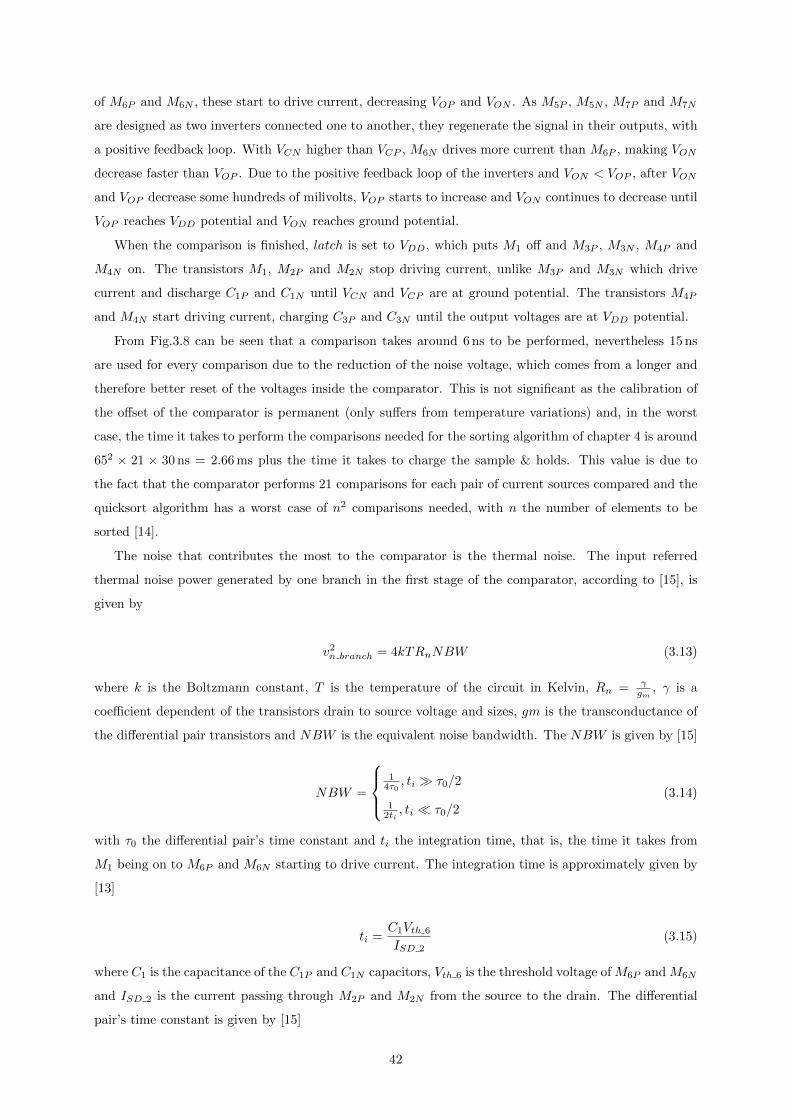
of M6P and M6N , these start to drive current, decreasing VOP and VON . As M5P , M5N , M7P and M7N
are designed as two inverters connected one to another, they regenerate the signal in their outputs, with
a positive feedback loop. With VCN higher than VCP , M6N drives more current than M6P , making VON
decrease faster than VOP . Due to the positive feedback loop of the inverters and VON < VOP , after VON
and VOP decrease some hundreds of milivolts, VOP starts to increase and VON continues to decrease until
VOP reaches VDD potential and VON reaches ground potential.
When the comparison is finished, latch is set to VDD, which puts M1 off and M3P , M3N , M4P and
M4N on. The transistors M1, M2P and M2N stop driving current, unlike M3P and M3N which drive
current and discharge C1P and C1N until VCN and VCP are at ground potential. The transistors M4P
and M4N start driving current, charging C3P and C3N until the output voltages are at VDD potential.
From Fig.3.8 can be seen that a comparison takes around 6 ns to be performed, nevertheless 15 ns
are used for every comparison due to the reduction of the noise voltage, which comes from a longer and
therefore better reset of the voltages inside the comparator. This is not significant as the calibration of
the offset of the comparator is permanent (only suffers from temperature variations) and, in the worst
case, the time it takes to perform the comparisons needed for the sorting algorithm of chapter 4 is around
652 × 21 × 30 ns = 2.66 ms plus the time it takes to charge the sample & holds. This value is due to
the fact that the comparator performs 21 comparisons for each pair of current sources compared and the
quicksort algorithm has a worst case of n2 comparisons needed, with n the number of elements to be
sorted [14].
The noise that contributes the most to the comparator is the thermal noise. The input referred
thermal noise power generated by one branch in the first stage of the comparator, according to [15], is
given by
v2n branch = 4kTRnNBW (3.13)
where k is the Boltzmann constant, T is the temperature of the circuit in Kelvin, Rn = γgm
, γ is a
coefficient dependent of the transistors drain to source voltage and sizes, gm is the transconductance of
the differential pair transistors and NBW is the equivalent noise bandwidth. The NBW is given by [15]
NBW =
1
4τ0, ti τ0/2
12ti, ti τ0/2
(3.14)
with τ0 the differential pair’s time constant and ti the integration time, that is, the time it takes from
M1 being on to M6P and M6N starting to drive current. The integration time is approximately given by
[13]
ti =C1Vth 6
ISD 2(3.15)
where C1 is the capacitance of the C1P and C1N capacitors, Vth 6 is the threshold voltage of M6P and M6N
and ISD 2 is the current passing through M2P and M2N from the source to the drain. The differential
pair’s time constant is given by [15]
42
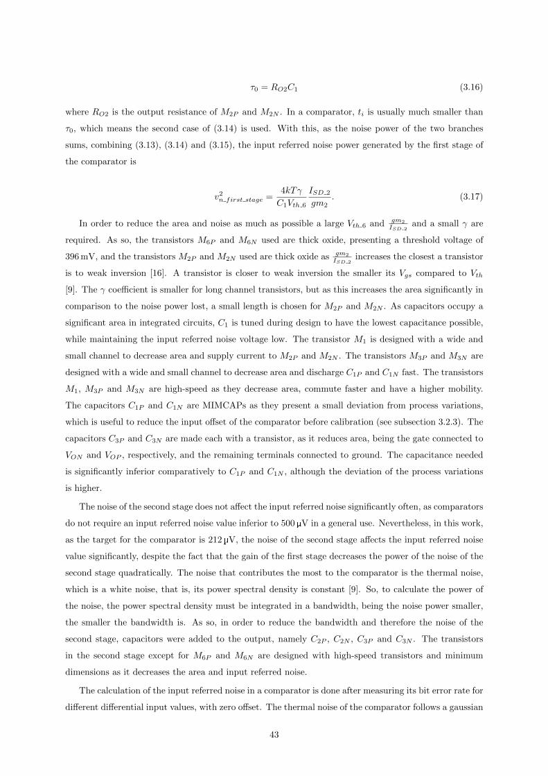
τ0 = RO2C1 (3.16)
where RO2 is the output resistance of M2P and M2N . In a comparator, ti is usually much smaller than
τ0, which means the second case of (3.14) is used. With this, as the noise power of the two branches
sums, combining (3.13), (3.14) and (3.15), the input referred noise power generated by the first stage of
the comparator is
v2n first stage =
4kTγ
C1Vth 6
ISD 2
gm2. (3.17)
In order to reduce the area and noise as much as possible a large Vth 6 and gm2
ISD 2and a small γ are
required. As so, the transistors M6P and M6N used are thick oxide, presenting a threshold voltage of
396 mV, and the transistors M2P and M2N used are thick oxide as gm2
ISD 2increases the closest a transistor
is to weak inversion [16]. A transistor is closer to weak inversion the smaller its Vgs compared to Vth
[9]. The γ coefficient is smaller for long channel transistors, but as this increases the area significantly in
comparison to the noise power lost, a small length is chosen for M2P and M2N . As capacitors occupy a
significant area in integrated circuits, C1 is tuned during design to have the lowest capacitance possible,
while maintaining the input referred noise voltage low. The transistor M1 is designed with a wide and
small channel to decrease area and supply current to M2P and M2N . The transistors M3P and M3N are
designed with a wide and small channel to decrease area and discharge C1P and C1N fast. The transistors
M1, M3P and M3N are high-speed as they decrease area, commute faster and have a higher mobility.
The capacitors C1P and C1N are MIMCAPs as they present a small deviation from process variations,
which is useful to reduce the input offset of the comparator before calibration (see subsection 3.2.3). The
capacitors C3P and C3N are made each with a transistor, as it reduces area, being the gate connected to
VON and VOP , respectively, and the remaining terminals connected to ground. The capacitance needed
is significantly inferior comparatively to C1P and C1N , although the deviation of the process variations
is higher.
The noise of the second stage does not affect the input referred noise significantly often, as comparators
do not require an input referred noise value inferior to 500µV in a general use. Nevertheless, in this work,
as the target for the comparator is 212µV, the noise of the second stage affects the input referred noise
value significantly, despite the fact that the gain of the first stage decreases the power of the noise of the
second stage quadratically. The noise that contributes the most to the comparator is the thermal noise,
which is a white noise, that is, its power spectral density is constant [9]. So, to calculate the power of
the noise, the power spectral density must be integrated in a bandwidth, being the noise power smaller,
the smaller the bandwidth is. As so, in order to reduce the bandwidth and therefore the noise of the
second stage, capacitors were added to the output, namely C2P , C2N , C3P and C3N . The transistors
in the second stage except for M6P and M6N are designed with high-speed transistors and minimum
dimensions as it decreases the area and input referred noise.
The calculation of the input referred noise in a comparator is done after measuring its bit error rate for
different differential input values, with zero offset. The thermal noise of the comparator follows a gaussian
43
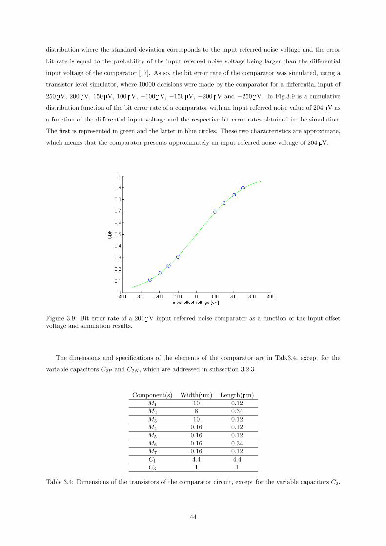
distribution where the standard deviation corresponds to the input referred noise voltage and the error
bit rate is equal to the probability of the input referred noise voltage being larger than the differential
input voltage of the comparator [17]. As so, the bit error rate of the comparator was simulated, using a
transistor level simulator, where 10000 decisions were made by the comparator for a differential input of
250 µV, 200 µV, 150 µV, 100 µV, −100 µV, −150 µV, −200 µV and −250 µV. In Fig.3.9 is a cumulative
distribution function of the bit error rate of a comparator with an input referred noise value of 204µV as
a function of the differential input voltage and the respective bit error rates obtained in the simulation.
The first is represented in green and the latter in blue circles. These two characteristics are approximate,
which means that the comparator presents approximately an input referred noise voltage of 204 µV.
Figure 3.9: Bit error rate of a 204µV input referred noise comparator as a function of the input offsetvoltage and simulation results.
The dimensions and specifications of the elements of the comparator are in Tab.3.4, except for the
variable capacitors C2P and C2N , which are addressed in subsection 3.2.3.
Component(s) Width(µm) Length(µm)M1 10 0.12M2 8 0.34M3 10 0.12M4 0.16 0.12M5 0.16 0.12M6 0.16 0.34M7 0.16 0.12C1 4.4 4.4C3 1 1
Table 3.4: Dimensions of the transistors of the comparator circuit, except for the variable capacitors C2.
44
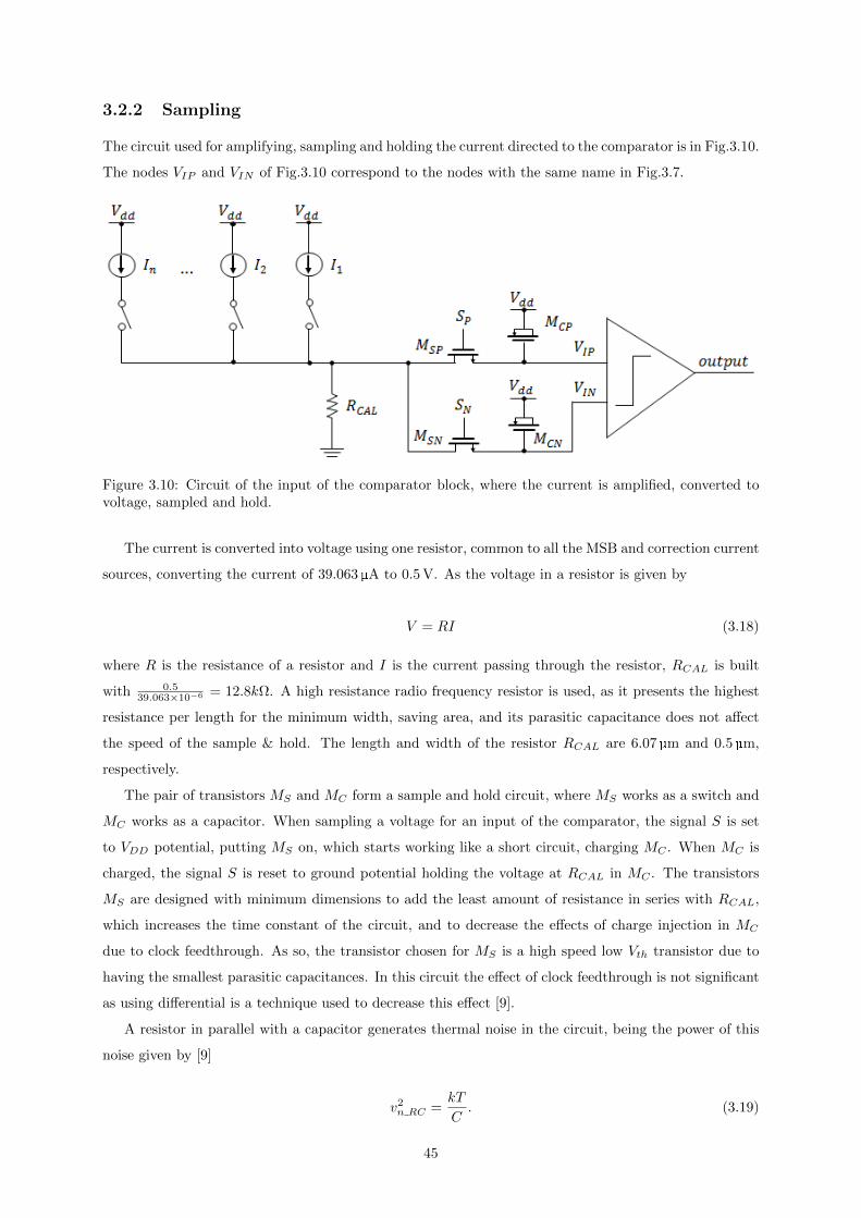
3.2.2 Sampling
The circuit used for amplifying, sampling and holding the current directed to the comparator is in Fig.3.10.
The nodes VIP and VIN of Fig.3.10 correspond to the nodes with the same name in Fig.3.7.
Figure 3.10: Circuit of the input of the comparator block, where the current is amplified, converted tovoltage, sampled and hold.
The current is converted into voltage using one resistor, common to all the MSB and correction current
sources, converting the current of 39.063 µA to 0.5 V. As the voltage in a resistor is given by
V = RI (3.18)
where R is the resistance of a resistor and I is the current passing through the resistor, RCAL is built
with 0.539.063×10−6 = 12.8kΩ. A high resistance radio frequency resistor is used, as it presents the highest
resistance per length for the minimum width, saving area, and its parasitic capacitance does not affect
the speed of the sample & hold. The length and width of the resistor RCAL are 6.07 µm and 0.5µm,
respectively.
The pair of transistors MS and MC form a sample and hold circuit, where MS works as a switch and
MC works as a capacitor. When sampling a voltage for an input of the comparator, the signal S is set
to VDD potential, putting MS on, which starts working like a short circuit, charging MC . When MC is
charged, the signal S is reset to ground potential holding the voltage at RCAL in MC . The transistors
MS are designed with minimum dimensions to add the least amount of resistance in series with RCAL,
which increases the time constant of the circuit, and to decrease the effects of charge injection in MC
due to clock feedthrough. As so, the transistor chosen for MS is a high speed low Vth transistor due to
having the smallest parasitic capacitances. In this circuit the effect of clock feedthrough is not significant
as using differential is a technique used to decrease this effect [9].
A resistor in parallel with a capacitor generates thermal noise in the circuit, being the power of this
noise given by [9]
v2n RC =
kT
C. (3.19)
45
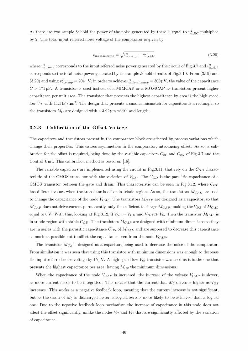
As there are two sample & hold the power of the noise generated by these is equal to v2n RC multiplied
by 2. The total input referred noise voltage of the comparator is given by
vn total comp =√v2n comp + v2
n s&h. (3.20)
where v2n comp corresponds to the input referred noise power generated by the circuit of Fig.3.7 and v2
n s&h
corresponds to the total noise power generated by the sample & hold circuits of Fig.3.10. From (3.19) and
(3.20) and using v2n comp = 204µV, in order to achieve v2
n total comp = 300µV, the value of the capacitance
C is 171 pF. A transistor is used instead of a MIMCAP or a MOMCAP as transistors present higher
capacitance per unit area. The transistor that presents the highest capacitance by area is the high speed
low Vth with 11.1 fF /µm2. The design that presents a smaller mismatch for capacitors is a rectangle, so
the transistors MC are designed with a 3.92 µm width and length.
3.2.3 Calibration of the Offset Voltage
The capacitors and transistors present in the comparator block are affected by process variations which
change their properties. This causes asymmetries in the comparator, introducing offset. As so, a cali-
bration for the offset is required, being done by the variable capacitors C2P and C2N of Fig.3.7 and the
Control Unit. This calibration method is based on [18].
The variable capacitors are implemented using the circuit in Fig.3.11, that rely on the CGD charac-
teristic of the CMOS transistor with the variation of VGS . The CGD is the parasitic capacitance of a
CMOS transistor between the gate and drain. This characteristic can be seen in Fig.3.12, where CGD
has different values when the transistor is off or in triode region. As so, the transistors MCAL are used
to change the capacitance of the node VCAL. The transistors MCAP are designed as a capacitor, so that
MCAP does not drive current permanently, only the sufficient to charge MCAP , making the VDS of MCAL
equal to 0 V. With this, looking at Fig.3.12, if VGS = VDD and VDD Vth, then the transistor MCAL is
in triode region with stable CGD. The transistors MCAP are designed with minimum dimensions as they
are in series with the parasitic capacitance CDS of MCAL and are supposed to decrease this capacitance
as much as possible not to affect the capacitance seen from the node VCAP .
The transistor MC2 is designed as a capacitor, being used to decrease the noise of the comparator.
From simulation it was seen that using this transistor with minimum dimensions was enough to decrease
the input referred noise voltage by 15µV. A high speed low Vth transistor was used as it is the one that
presents the highest capacitance per area, having MC2 the minimum dimensions.
When the capacitance of the node VCAP is increased, the increase of the voltage VCAP is slower,
as more current needs to be integrated. This means that the current that M6 drives is higher as VGS
increases. This works as a negative feedback loop, meaning that the current increase is not significant,
but as the drain of M6 is discharged faster, a logical zero is more likely to be achieved than a logical
one. Due to the negative feedback loop mechanism the increase of capacitance in this node does not
affect the offset significantly, unlike the nodes VC and VO that are significantly affected by the variation
of capacitance.
46
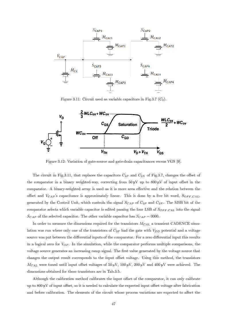
Figure 3.11: Circuit used as variable capacitors in Fig.3.7 (C2).
Figure 3.12: Variation of gate-source and gate-drain capacitances versus VGS [9].
The circuit in Fig.3.11, that replaces the capacitors C2P and C2N of Fig.3.7, changes the offset of
the comparator in a binary weighted-way, correcting from 50 µV up to 800µV of input offset in the
comparator. A binary-weighted array is used as it is more area effective and the relation between the
offset and VCAP ’s capacitance is approximately linear. This is done by a five bit word, SOFF CAL,
generated by the Control Unit, which controls the signal SCAP of C2P and C2N . The MSB bit of the
comparator selects which variable capacitor is edited passing the four LSB of SOFF CAL into the signal
SCAP of the selected capacitor. The other variable capacitor has SCAP = 0000.
In order to measure the dimensions required for the transistors MCAL a transient CADENCE simu-
lation was run where only one of the transistors of C2P had the gate with VDD potential and a voltage
source was put between the differential inputs of the comparator. For a zero differential input this results
in a logical zero for VOP . In the simulation, while the comparator performs multiple comparisons, the
voltage source generates an increasing ramp signal. The first value generated by the voltage source that
changes the output result corresponds to the input offset voltage. Using this method, the transistors
MCAL were tuned until input offset voltages of 50µV, 100 µV, 200 µV and 400 µV were achieved. The
dimensions obtained for these transistors are in Tab.3.5.
Although the calibration method calibrates the input offset of the comparator, it can only calibrate
up to 800 µV of input offset, so it is needed to calculate the expected input offset voltage after fabrication
and before calibration. The elements of the circuit whose process variations are expected to affect the
47
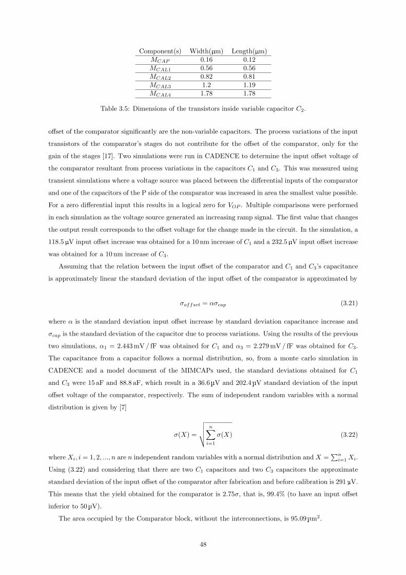
Component(s) Width(µm) Length(µm)MCAP 0.16 0.12MCAL1 0.56 0.56MCAL2 0.82 0.81MCAL3 1.2 1.19MCAL4 1.78 1.78
Table 3.5: Dimensions of the transistors inside variable capacitor C2.
offset of the comparator significantly are the non-variable capacitors. The process variations of the input
transistors of the comparator’s stages do not contribute for the offset of the comparator, only for the
gain of the stages [17]. Two simulations were run in CADENCE to determine the input offset voltage of
the comparator resultant from process variations in the capacitors C1 and C3. This was measured using
transient simulations where a voltage source was placed between the differential inputs of the comparator
and one of the capacitors of the P side of the comparator was increased in area the smallest value possible.
For a zero differential input this results in a logical zero for VOP . Multiple comparisons were performed
in each simulation as the voltage source generated an increasing ramp signal. The first value that changes
the output result corresponds to the offset voltage for the change made in the circuit. In the simulation, a
118.5µV input offset increase was obtained for a 10 nm increase of C1 and a 232.5µV input offset increase
was obtained for a 10 nm increase of C3.
Assuming that the relation between the input offset of the comparator and C1 and C3’s capacitance
is approximately linear the standard deviation of the input offset of the comparator is approximated by
σoffset = ασcap (3.21)
where α is the standard deviation input offset increase by standard deviation capacitance increase and
σcap is the standard deviation of the capacitor due to process variations. Using the results of the previous
two simulations, α1 = 2.443 mV / fF was obtained for C1 and α3 = 2.279 mV / fF was obtained for C3.
The capacitance from a capacitor follows a normal distribution, so, from a monte carlo simulation in
CADENCE and a model document of the MIMCAPs used, the standard deviations obtained for C1
and C3 were 15 aF and 88.8 aF, which result in a 36.6 µV and 202.4 µV standard deviation of the input
offset voltage of the comparator, respectively. The sum of independent random variables with a normal
distribution is given by [7]
σ(X) =
√√√√ n∑i=1
σ(X) (3.22)
where Xi, i = 1, 2, ..., n are n independent random variables with a normal distribution and X =∑ni=1Xi.
Using (3.22) and considering that there are two C1 capacitors and two C3 capacitors the approximate
standard deviation of the input offset of the comparator after fabrication and before calibration is 291 µV.
This means that the yield obtained for the comparator is 2.75σ, that is, 99.4% (to have an input offset
inferior to 50µV).
The area occupied by the Comparator block, without the interconnections, is 95.09 µm2.
48
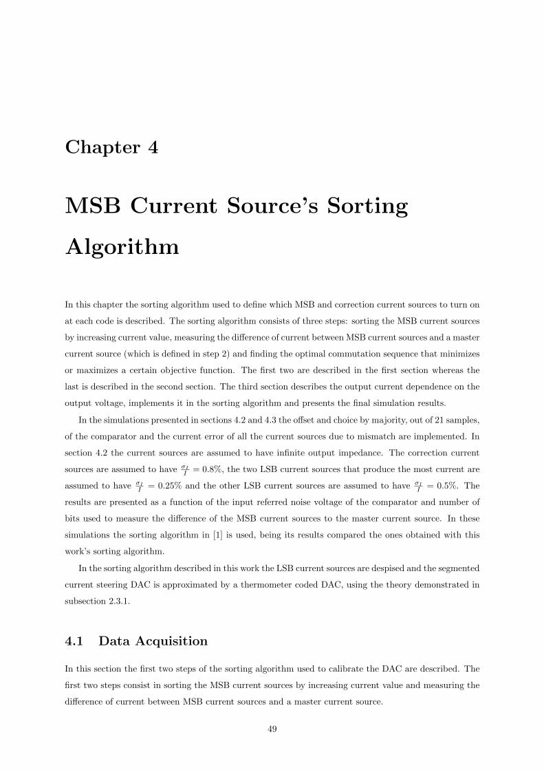
Chapter 4
MSB Current Source’s Sorting
Algorithm
In this chapter the sorting algorithm used to define which MSB and correction current sources to turn on
at each code is described. The sorting algorithm consists of three steps: sorting the MSB current sources
by increasing current value, measuring the difference of current between MSB current sources and a master
current source (which is defined in step 2) and finding the optimal commutation sequence that minimizes
or maximizes a certain objective function. The first two are described in the first section whereas the
last is described in the second section. The third section describes the output current dependence on the
output voltage, implements it in the sorting algorithm and presents the final simulation results.
In the simulations presented in sections 4.2 and 4.3 the offset and choice by majority, out of 21 samples,
of the comparator and the current error of all the current sources due to mismatch are implemented. In
section 4.2 the current sources are assumed to have infinite output impedance. The correction current
sources are assumed to have σI
I = 0.8%, the two LSB current sources that produce the most current are
assumed to have σI
I = 0.25% and the other LSB current sources are assumed to have σI
I = 0.5%. The
results are presented as a function of the input referred noise voltage of the comparator and number of
bits used to measure the difference of the MSB current sources to the master current source. In these
simulations the sorting algorithm in [1] is used, being its results compared the ones obtained with this
work’s sorting algorithm.
In the sorting algorithm described in this work the LSB current sources are despised and the segmented
current steering DAC is approximated by a thermometer coded DAC, using the theory demonstrated in
subsection 2.3.1.
4.1 Data Acquisition
In this section the first two steps of the sorting algorithm used to calibrate the DAC are described. The
first two steps consist in sorting the MSB current sources by increasing current value and measuring the
difference of current between MSB current sources and a master current source.
49
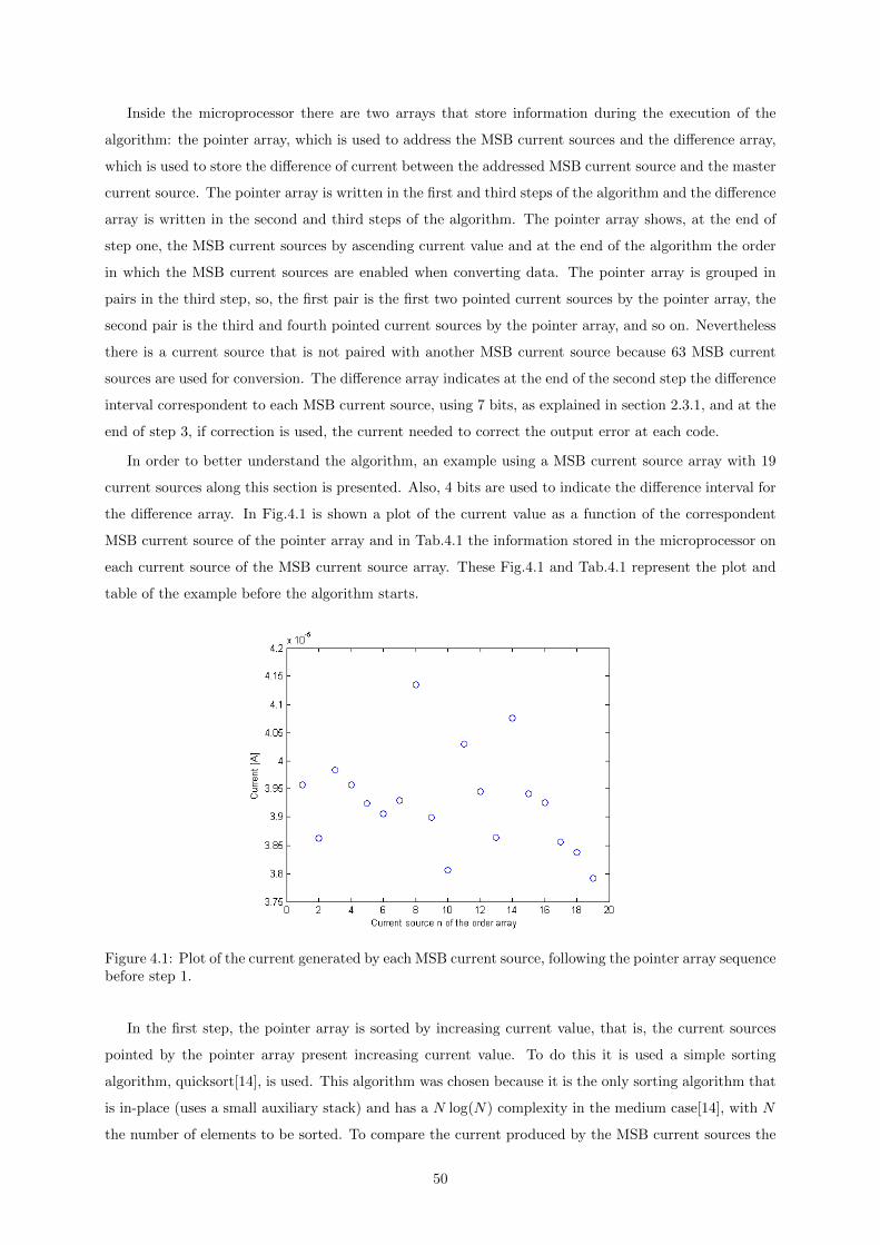
Inside the microprocessor there are two arrays that store information during the execution of the
algorithm: the pointer array, which is used to address the MSB current sources and the difference array,
which is used to store the difference of current between the addressed MSB current source and the master
current source. The pointer array is written in the first and third steps of the algorithm and the difference
array is written in the second and third steps of the algorithm. The pointer array shows, at the end of
step one, the MSB current sources by ascending current value and at the end of the algorithm the order
in which the MSB current sources are enabled when converting data. The pointer array is grouped in
pairs in the third step, so, the first pair is the first two pointed current sources by the pointer array, the
second pair is the third and fourth pointed current sources by the pointer array, and so on. Nevertheless
there is a current source that is not paired with another MSB current source because 63 MSB current
sources are used for conversion. The difference array indicates at the end of the second step the difference
interval correspondent to each MSB current source, using 7 bits, as explained in section 2.3.1, and at the
end of step 3, if correction is used, the current needed to correct the output error at each code.
In order to better understand the algorithm, an example using a MSB current source array with 19
current sources along this section is presented. Also, 4 bits are used to indicate the difference interval for
the difference array. In Fig.4.1 is shown a plot of the current value as a function of the correspondent
MSB current source of the pointer array and in Tab.4.1 the information stored in the microprocessor on
each current source of the MSB current source array. These Fig.4.1 and Tab.4.1 represent the plot and
table of the example before the algorithm starts.
Figure 4.1: Plot of the current generated by each MSB current source, following the pointer array sequencebefore step 1.
In the first step, the pointer array is sorted by increasing current value, that is, the current sources
pointed by the pointer array present increasing current value. To do this it is used a simple sorting
algorithm, quicksort[14], is used. This algorithm was chosen because it is the only sorting algorithm that
is in-place (uses a small auxiliary stack) and has a N log(N) complexity in the medium case[14], with N
the number of elements to be sorted. To compare the current produced by the MSB current sources the
50
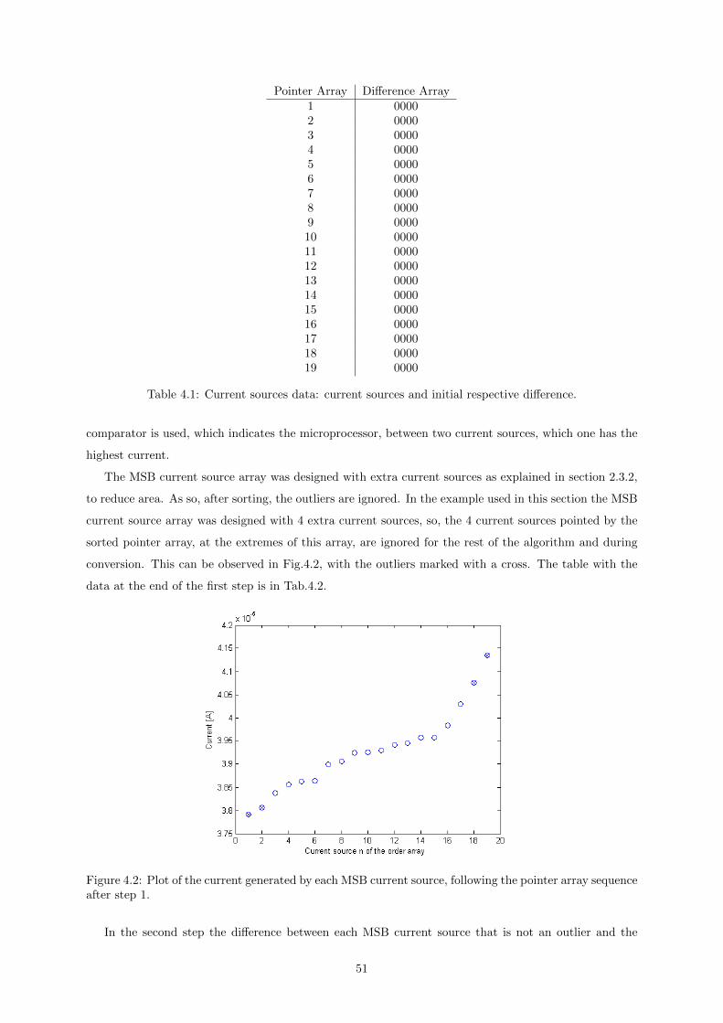
Pointer Array Difference Array1 00002 00003 00004 00005 00006 00007 00008 00009 000010 000011 000012 000013 000014 000015 000016 000017 000018 000019 0000
Table 4.1: Current sources data: current sources and initial respective difference.
comparator is used, which indicates the microprocessor, between two current sources, which one has the
highest current.
The MSB current source array was designed with extra current sources as explained in section 2.3.2,
to reduce area. As so, after sorting, the outliers are ignored. In the example used in this section the MSB
current source array was designed with 4 extra current sources, so, the 4 current sources pointed by the
sorted pointer array, at the extremes of this array, are ignored for the rest of the algorithm and during
conversion. This can be observed in Fig.4.2, with the outliers marked with a cross. The table with the
data at the end of the first step is in Tab.4.2.
Figure 4.2: Plot of the current generated by each MSB current source, following the pointer array sequenceafter step 1.
In the second step the difference between each MSB current source that is not an outlier and the
51

Pointer Array Difference Array19 000010 000018 000017 00002 000013 00009 00006 00005 000016 00007 000015 000012 00004 00001 00003 000011 000014 00008 0000
Table 4.2: Current sources data: current sources by ascending current value.
master current source is measured and stored in the difference array. The MSB current source with
the median current value is assumed to be the one that produces the current closest to the value of a
quantization step, and therefore, is considered the master current source. So, the difference is calculated
in comparison to the master current source. There are 128 difference intervals in which the MSB current
sources are expected to be in, and whose boundaries are defined by the correction current sources in
parallel with the master current source. In the example, as the difference is measured with 4 bits there
are 16 difference intervals. These intervals can be seen in Fig.4.3 where the boundaries of each interval
are represented by horizontal lines.
Figure 4.3: Plot of the current generated by each MSB current source, following the pointer arraysequence, and difference interval limits after step 2.
The least significant bits of the difference array indicate the module of the approximate value of
52

the difference between the master current source and the current source pointed by the pointer array,
measured in 2−5 LSB of current, which will be called dstep from now on. The most significant bit of the
difference array is 0 or 1, depending if the difference is positive or negative, respectively. For instance,
in Fig.4.3, it can be seen that the current source with the smallest current value is five dstep below the
master current source, which is marked as a magenta circle. As so, the value stored in the difference
array for this current source is 0101. The values stored for each current source can be seen in Tab.4.3.
Notice that the master current source does not have a value in the difference array as it is not needed
and that the first two and last two current sources that were in the difference array of Tab.4.2 are no
longer in Tab.4.3 as they are outliers.
Pointer Array Difference Array18 010117 01002 010013 00119 00016 00015 000016 ——7 100015 100112 10014 10101 10103 101111 1110
Table 4.3: Current sources data: current sources by ascending current value and respective difference.
The algorithm used to write the difference array calculates the difference interval that the first current
source pointed by the sorted pointer array is in. After that, it is checked if the second current source
pointed by the sorted pointer array is in the same difference interval as the previous current source, that
is, the first one pointed in the sorted pointer array. This method is then applied to the other current
sources present in the pointer array in order. If one current source is not in the same difference interval
as the previously pointed, then it is checked if the current source is in the next difference interval with
a higher current, passing to the next if it is not, until it is found in which difference interval the current
source is, or the last difference interval is reached.
To calculate the difference interval associated with each current source, correction current sources are
turned on in parallel with the master current source. It is considered that there is an error equal to
zero when the master current source is enabled in parallel with 2 correction current sources that produce
1 LSB. If the difference to be measured is smaller than zero, then a current inferior to 2 LSB is produced
by the Correction Array Block, otherwise a higher current is produced.
The green lines in Fig.4.3 represent the different current values that correction current sources can
produce in parallel with the master current source on. To determine if one current source is within one
difference interval its current is compared with the upper and lower boundaries, in case they exist. The
red boundaries can not be compared because they cannot be produced, they indicate the interval where
53
it is expected to find all the current sources, with exception of the outliers.
After calculating the arrays, the microprocessor applies the third step, that is, the algorithm described
in the next section, using data similar to Tab.4.3 as input and targeting to minimize or maximize a desired
specification.
4.2 Optimal Commutation Sequence
In this section the algorithm that finds the optimal commutation sequence to use in the DAC is described,
corresponding to the step 3 of the sorting algorithm. This commutation sequence is applied to the MSB
current sources, and in the case correction is used, to the latter and to the correction current sources.
In subsection 4.2.1 a description of the algorithm without the use of correction is made and in sub-
section 4.2.2 the INL code correction is implemented. The algorithms that are described in this section
are exclusively performed by the microprocessor.
4.2.1 MSB Commutation Sequence
The algorithm that finds the optimal commutation sequence for a desired performance starts by making
an estimate of the difference value of each MSB current source to the master current source based on
the pointer and difference arrays, then groups the current sources of the pointer array in pairs and ends
searching for the commutation sequence that minimizes or maximizes a desired performance.
To estimate the difference of each MSB current source to the master current source the difference
interval in which a current source is in and how many current sources are in it is verified. Let a difference
step correspond to the difference of current between the boundaries of an error interval. If a current
source has −2 in the difference array, it means that the difference of current between a current source
and the master current source is between −3 and −2 dstep. If this current source is the only one within
this difference interval, then its approximate mean error value is −2.5dstep. If there are more current
sources within the difference interval of this current source whose error is being estimated, then the
approximate mean error value of the current source whose difference is being estimated will depend on
the number of current sources inside the difference interval and on the number of current sources inside
the difference interval that produce less or more current than the current source whose difference is being
estimated. The approximate mean difference of the current source k of the pointer array is calculated in
the algorithm with
dest[k] =ndif smaller[k] + 1
ndif [k] + 1+ dmes[k] (4.1)
where dest is the array with the approximate mean difference of the MSB current sources, dmes is the mea-
sured difference array, ndif [k] is the number of current sources with the value dmes[k] and ndif smaller[k]
is the number of current sources with the value dmes[k] and smaller difference than the current source k
(this is verified with the pointer array). For instance, if there are two MSB current sources with dmes = 4
then their estimated difference value dest is 4 + 13 and 4 + 2
3 , being the second value attributed to the
54
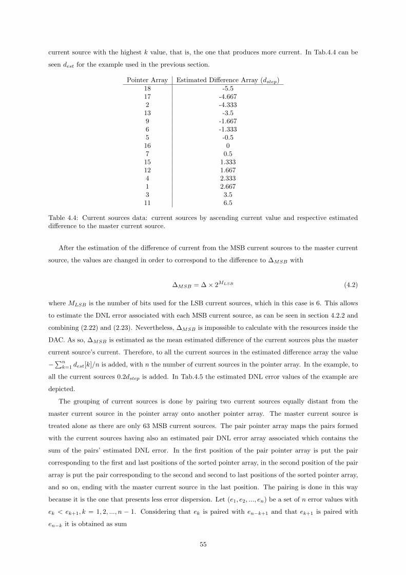
current source with the highest k value, that is, the one that produces more current. In Tab.4.4 can be
seen dest for the example used in the previous section.
Pointer Array Estimated Difference Array (dstep)18 -5.517 -4.6672 -4.33313 -3.59 -1.6676 -1.3335 -0.516 07 0.515 1.33312 1.6674 2.3331 2.6673 3.511 6.5
Table 4.4: Current sources data: current sources by ascending current value and respective estimateddifference to the master current source.
After the estimation of the difference of current from the MSB current sources to the master current
source, the values are changed in order to correspond to the difference to ∆MSB with
∆MSB = ∆× 2MLSB (4.2)
where MLSB is the number of bits used for the LSB current sources, which in this case is 6. This allows
to estimate the DNL error associated with each MSB current source, as can be seen in section 4.2.2 and
combining (2.22) and (2.23). Nevertheless, ∆MSB is impossible to calculate with the resources inside the
DAC. As so, ∆MSB is estimated as the mean estimated difference of the current sources plus the master
current source’s current. Therefore, to all the current sources in the estimated difference array the value
−∑nk=1 dest[k]/n is added, with n the number of current sources in the pointer array. In the example, to
all the current sources 0.2dstep is added. In Tab.4.5 the estimated DNL error values of the example are
depicted.
The grouping of current sources is done by pairing two current sources equally distant from the
master current source in the pointer array onto another pointer array. The master current source is
treated alone as there are only 63 MSB current sources. The pair pointer array maps the pairs formed
with the current sources having also an estimated pair DNL error array associated which contains the
sum of the pairs’ estimated DNL error. In the first position of the pair pointer array is put the pair
corresponding to the first and last positions of the sorted pointer array, in the second position of the pair
array is put the pair corresponding to the second and second to last positions of the sorted pointer array,
and so on, ending with the master current source in the last position. The pairing is done in this way
because it is the one that presents less error dispersion. Let (e1, e2, ..., en) be a set of n error values with
ek < ek+1, k = 1, 2, ..., n − 1. Considering that ek is paired with en−k+1 and that ek+1 is paired with
en−k it is obtained as sum
55
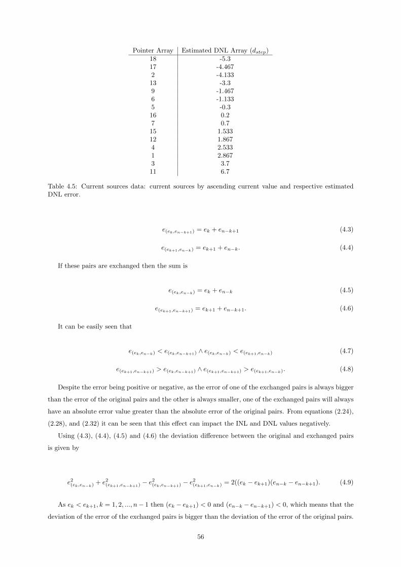
Pointer Array Estimated DNL Array (dstep)18 -5.317 -4.4672 -4.13313 -3.39 -1.4676 -1.1335 -0.316 0.27 0.715 1.53312 1.8674 2.5331 2.8673 3.711 6.7
Table 4.5: Current sources data: current sources by ascending current value and respective estimatedDNL error.
e(ek,en−k+1) = ek + en−k+1 (4.3)
e(ek+1,en−k) = ek+1 + en−k. (4.4)
If these pairs are exchanged then the sum is
e(ek,en−k) = ek + en−k (4.5)
e(ek+1,en−k+1) = ek+1 + en−k+1. (4.6)
It can be easily seen that
e(ek,en−k) < e(ek,en−k+1) ∧ e(ek,en−k) < e(ek+1,en−k) (4.7)
e(ek+1,en−k+1) > e(ek,en−k+1) ∧ e(ek+1,en−k+1) > e(ek+1,en−k). (4.8)
Despite the error being positive or negative, as the error of one of the exchanged pairs is always bigger
than the error of the original pairs and the other is always smaller, one of the exchanged pairs will always
have an absolute error value greater than the absolute error of the original pairs. From equations (2.24),
(2.28), and (2.32) it can be seen that this effect can impact the INL and DNL values negatively.
Using (4.3), (4.4), (4.5) and (4.6) the deviation difference between the original and exchanged pairs
is given by
e2(ek,en−k) + e2
(ek+1,en−k+1) − e2(ek,en−k+1) − e
2(ek+1,en−k) = 2((ek − ek+1)(en−k − en−k+1). (4.9)
As ek < ek+1, k = 1, 2, ..., n− 1 then (ek − ek+1) < 0 and (en−k − en−k+1) < 0, which means that the
deviation of the error of the exchanged pairs is bigger than the deviation of the error of the original pairs.
56
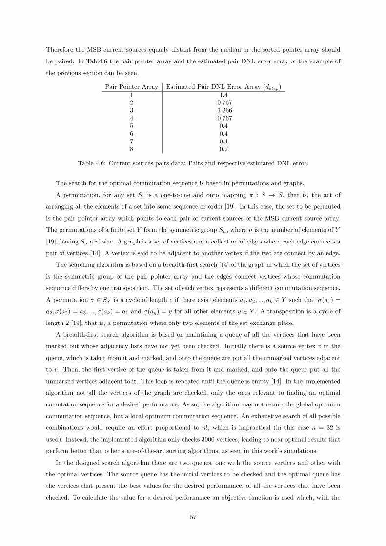
Therefore the MSB current sources equally distant from the median in the sorted pointer array should
be paired. In Tab.4.6 the pair pointer array and the estimated pair DNL error array of the example of
the previous section can be seen.
Pair Pointer Array Estimated Pair DNL Error Array (dstep)1 1.42 -0.7673 -1.2664 -0.7675 0.46 0.47 0.48 0.2
Table 4.6: Current sources pairs data: Pairs and respective estimated DNL error.
The search for the optimal commutation sequence is based in permutations and graphs.
A permutation, for any set S, is a one-to-one and onto mapping π : S → S, that is, the act of
arranging all the elements of a set into some sequence or order [19]. In this case, the set to be permuted
is the pair pointer array which points to each pair of current sources of the MSB current source array.
The permutations of a finite set Y form the symmetric group Sn, where n is the number of elements of Y
[19], having Sn a n! size. A graph is a set of vertices and a collection of edges where each edge connects a
pair of vertices [14]. A vertex is said to be adjacent to another vertex if the two are connect by an edge.
The searching algorithm is based on a breadth-first search [14] of the graph in which the set of vertices
is the symmetric group of the pair pointer array and the edges connect vertices whose commutation
sequence differs by one transposition. The set of each vertex represents a different commutation sequence.
A permutation σ ∈ SY is a cycle of length c if there exist elements a1, a2, ..., ak ∈ Y such that σ(a1) =
a2, σ(a2) = a3, ..., σ(ak) = a1 and σ(ay) = y for all other elements y ∈ Y . A transposition is a cycle of
length 2 [19], that is, a permutation where only two elements of the set exchange place.
A breadth-first search algorithm is based on maintining a queue of all the vertices that have been
marked but whose adjacency lists have not yet been checked. Initially there is a source vertex v in the
queue, which is taken from it and marked, and onto the queue are put all the unmarked vertices adjacent
to v. Then, the first vertice of the queue is taken from it and marked, and onto the queue put all the
unmarked vertices adjacent to it. This loop is repeated until the queue is empty [14]. In the implemented
algorithm not all the vertices of the graph are checked, only the ones relevant to finding an optimal
comutation sequence for a desired performance. As so, the algorithm may not return the global optimum
commutation sequence, but a local optimum commutation sequence. An exhaustive search of all possible
combinations would require an effort proportional to n!, which is impractical (in this case n = 32 is
used). Instead, the implemented algorithm only checks 3000 vertices, leading to near optimal results that
perform better than other state-of-the-art sorting algorithms, as seen in this work’s simulations.
In the designed search algorithm there are two queues, one with the source vertices and other with
the optimal vertices. The source queue has the initial vertices to be checked and the optimal queue has
the vertices that present the best values for the desired performance, of all the vertices that have been
checked. To calculate the value for a desired performance an objective function is used which, with the
57
vertice’s set and estimated pair DNL error array as input, returns a value proportional to the performance
that is desired to be optimized.
The source queue has the vertices by which the search begins. The more vertices there are in the
source queue and the bigger the number of transpositions between each, the better the graph will be
searched, as it starts from “distant” vertices, having more chances of converging to better local optima.
The vertices put in the queue are shifts of the pair pointer array. For instance, in the example the
source vertices would be 1, 2, 3, 4, 5, 6, 7, 8, 2, 3, 4, 5, 6, 7, 8, 1, ..., 8, 1, 2, 3, 4, 5, 6, 7. A cycle of length
c requires at least round( c2 ) transpositions to invert the permutation as c elements are out of place and
a transposition can only return two elements to their original place. As the permutation from one source
vertex to another is a cycle of length(X), with length(S) the length of the set S and X the set of a
vertex, this method was chosen.
The optimal queue has the vertices that present the best values for the desired performance, in
ascending order. The algorithm starts with the worst possible value in every position of the optimal
queue and no sets. In the beginning of the search, the following loop is run: a vertex is removed from the
source queue, marked, it’s value is calculated using the objective function, and it is checked if the value
obtained is better or worse than the first position of the optimal queue. If it is better, then the vertex is
inserted in the queue and the vertices with worse values are shifted, being the worst, this is, the first of
the queue, removed. Otherwise the vertex is not put on the queue. After this, the values of the adjacent
vertices of the removed source vertex are calculated, being put in the optimal queue only the vertices
that have the best values. These adjacent vertices, which are unmarked, are put onto the optimal queue
in the same way as the source vertices. The loop only ends when the source queue is empty.
After this, the following loop is run: the first unmarked vertex of the optimal queue is marked. Then,
the unmarked adjacent vertices to this vertex are checked and put onto the queue, the same way as the
source vertices, if they present a better value than the first vertex of the optimal queue. This loop is
repeated until all the vertices in the optimal queue are marked. The optimal commutation sequence is the
one corresponding to the vertex in the last position of the queue. The pointed pairs in the pair pointer
array are then transformed back into the pair’s pointed current sources, being this the commutation
sequence used by the DAC. In Fig.4.4 and Fig.4.5 can be seen two flowcharts containing the search
algorithm. When transforming the pair’s pointed current sources back, the order of the current sources
inside the pair is immaterial because these are randomly enabled when only one needs to be enabled.
For instance, in the example, if the optimal commutation sequence found by the search algorithm is
4, 8, 1, 3, 5, 2, 6, 7, then the DAC’s optimal commutation sequence is the pointer array of Tab.4.7.
A simulation was done in MATLAB where 1000 random estimated pair DNL error arrays calculated
with 128 difference intervals were created. In this simulation the mean number of marked vertices in the
optimal queue and the mean optimal value obtained for the optimal commutation sequence as a function
of the dimension of the queue were calculated. The results can be seen in Fig.4.6 and Fig.4.7, respectively.
Due to the results it was chosen to use a 6 position queue because a bigger queue would improve the
optimal value by nearly 1%, which is not significant, and require more vertices to be marked, increasing
the computation time unnecessarily.
58
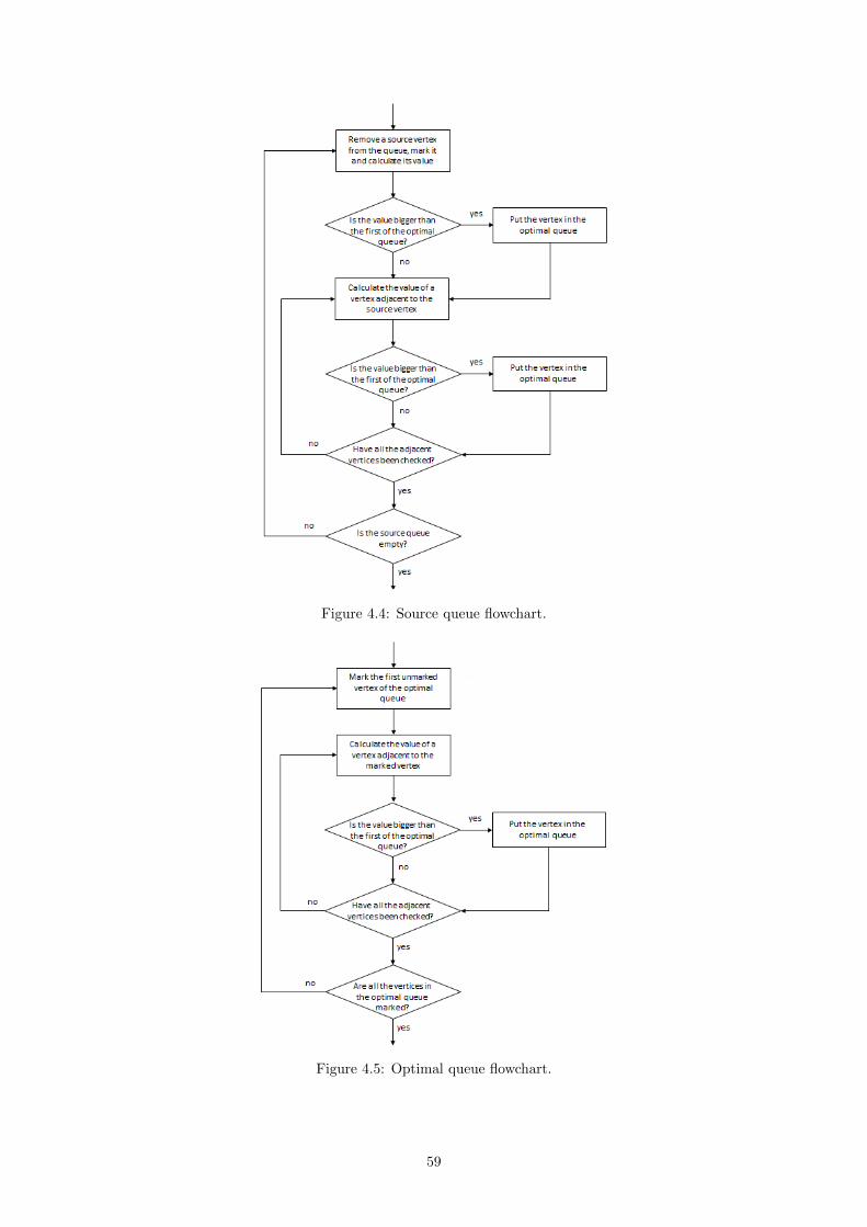
Figure 4.4: Source queue flowchart.
Figure 4.5: Optimal queue flowchart.
59
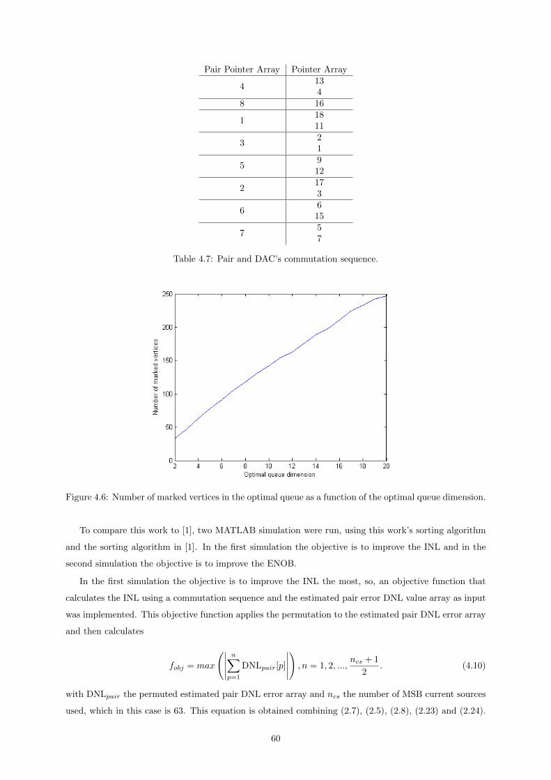
Pair Pointer Array Pointer Array
4134
8 16
11811
321
5912
2173
6615
757
Table 4.7: Pair and DAC’s commutation sequence.
Figure 4.6: Number of marked vertices in the optimal queue as a function of the optimal queue dimension.
To compare this work to [1], two MATLAB simulation were run, using this work’s sorting algorithm
and the sorting algorithm in [1]. In the first simulation the objective is to improve the INL and in the
second simulation the objective is to improve the ENOB.
In the first simulation the objective is to improve the INL the most, so, an objective function that
calculates the INL using a commutation sequence and the estimated pair error DNL value array as input
was implemented. This objective function applies the permutation to the estimated pair DNL error array
and then calculates
fobj = max
(∣∣∣∣∣n∑p=1
DNLpair[p]
∣∣∣∣∣), n = 1, 2, ...,
ncs + 1
2. (4.10)
with DNLpair the permuted estimated pair DNL error array and ncs the number of MSB current sources
used, which in this case is 63. This equation is obtained combining (2.7), (2.5), (2.8), (2.23) and (2.24).
60
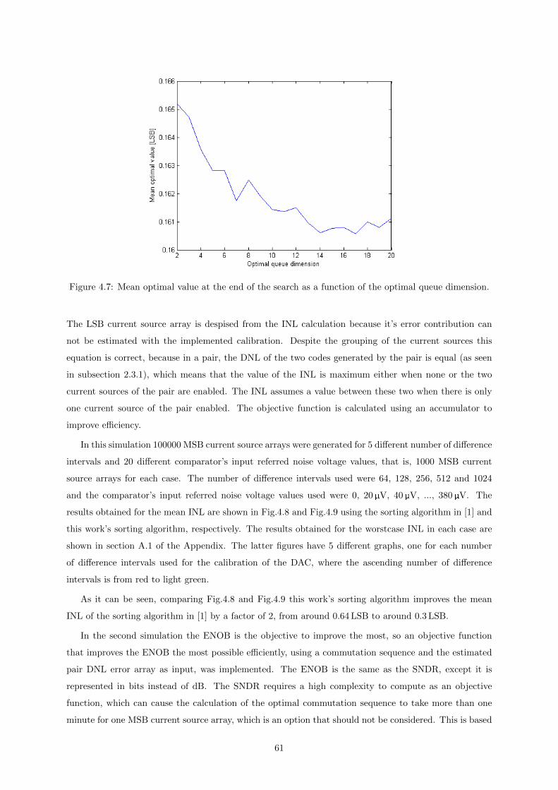
Figure 4.7: Mean optimal value at the end of the search as a function of the optimal queue dimension.
The LSB current source array is despised from the INL calculation because it’s error contribution can
not be estimated with the implemented calibration. Despite the grouping of the current sources this
equation is correct, because in a pair, the DNL of the two codes generated by the pair is equal (as seen
in subsection 2.3.1), which means that the value of the INL is maximum either when none or the two
current sources of the pair are enabled. The INL assumes a value between these two when there is only
one current source of the pair enabled. The objective function is calculated using an accumulator to
improve efficiency.
In this simulation 100000 MSB current source arrays were generated for 5 different number of difference
intervals and 20 different comparator’s input referred noise voltage values, that is, 1000 MSB current
source arrays for each case. The number of difference intervals used were 64, 128, 256, 512 and 1024
and the comparator’s input referred noise voltage values used were 0, 20 µV, 40µV, ..., 380 µV. The
results obtained for the mean INL are shown in Fig.4.8 and Fig.4.9 using the sorting algorithm in [1] and
this work’s sorting algorithm, respectively. The results obtained for the worstcase INL in each case are
shown in section A.1 of the Appendix. The latter figures have 5 different graphs, one for each number
of difference intervals used for the calibration of the DAC, where the ascending number of difference
intervals is from red to light green.
As it can be seen, comparing Fig.4.8 and Fig.4.9 this work’s sorting algorithm improves the mean
INL of the sorting algorithm in [1] by a factor of 2, from around 0.64 LSB to around 0.3 LSB.
In the second simulation the ENOB is the objective to improve the most, so an objective function
that improves the ENOB the most possible efficiently, using a commutation sequence and the estimated
pair DNL error array as input, was implemented. The ENOB is the same as the SNDR, except it is
represented in bits instead of dB. The SNDR requires a high complexity to compute as an objective
function, which can cause the calculation of the optimal commutation sequence to take more than one
minute for one MSB current source array, which is an option that should not be considered. This is based
61
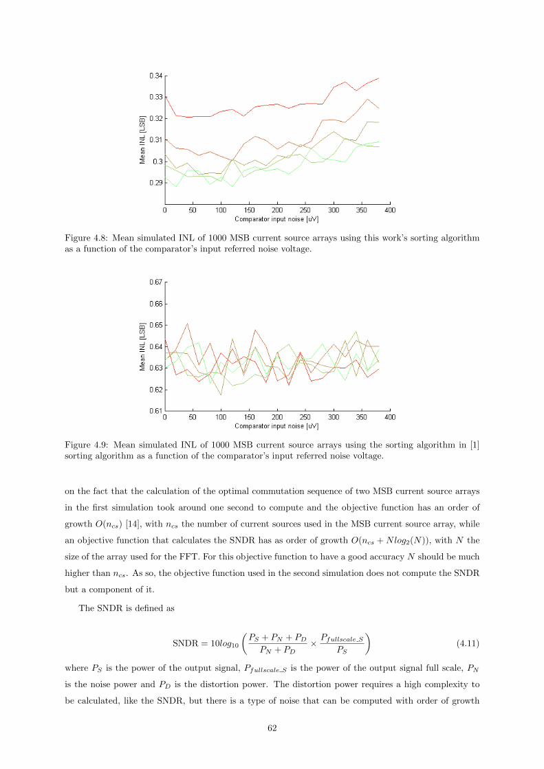
Figure 4.8: Mean simulated INL of 1000 MSB current source arrays using this work’s sorting algorithmas a function of the comparator’s input referred noise voltage.
Figure 4.9: Mean simulated INL of 1000 MSB current source arrays using the sorting algorithm in [1]sorting algorithm as a function of the comparator’s input referred noise voltage.
on the fact that the calculation of the optimal commutation sequence of two MSB current source arrays
in the first simulation took around one second to compute and the objective function has an order of
growth O(ncs) [14], with ncs the number of current sources used in the MSB current source array, while
an objective function that calculates the SNDR has as order of growth O(ncs +Nlog2(N)), with N the
size of the array used for the FFT. For this objective function to have a good accuracy N should be much
higher than ncs. As so, the objective function used in the second simulation does not compute the SNDR
but a component of it.
The SNDR is defined as
SNDR = 10log10
(PS + PN + PDPN + PD
× Pfullscale SPS
)(4.11)
where PS is the power of the output signal, Pfullscale S is the power of the output signal full scale, PN
is the noise power and PD is the distortion power. The distortion power requires a high complexity to
be calculated, like the SNDR, but there is a type of noise that can be computed with order of growth
62
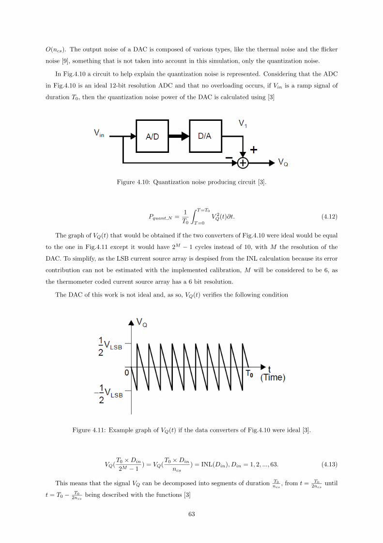
O(ncs). The output noise of a DAC is composed of various types, like the thermal noise and the flicker
noise [9], something that is not taken into account in this simulation, only the quantization noise.
In Fig.4.10 a circuit to help explain the quantization noise is represented. Considering that the ADC
in Fig.4.10 is an ideal 12-bit resolution ADC and that no overloading occurs, if Vin is a ramp signal of
duration T0, then the quantization noise power of the DAC is calculated using [3]
Figure 4.10: Quantization noise producing circuit [3].
Pquant N =1
T0
∫ T=T0
T=0
V 2Q(t)∂t. (4.12)
The graph of VQ(t) that would be obtained if the two converters of Fig.4.10 were ideal would be equal
to the one in Fig.4.11 except it would have 2M − 1 cycles instead of 10, with M the resolution of the
DAC. To simplify, as the LSB current source array is despised from the INL calculation because its error
contribution can not be estimated with the implemented calibration, M will be considered to be 6, as
the thermometer coded current source array has a 6 bit resolution.
The DAC of this work is not ideal and, as so, VQ(t) verifies the following condition
Figure 4.11: Example graph of VQ(t) if the data converters of Fig.4.10 were ideal [3].
VQ(T0 ×Din
2M − 1) = VQ(
T0 ×Din
ncs) = INL(Din), Din = 1, 2, ..., 63. (4.13)
This means that the signal VQ can be decomposed into segments of duration T0
ncs, from t = T0
2ncsuntil
t = T0 − T0
2ncsbeing described with the functions [3]
63
VQ Din(t) = ∆
(− t
T0+Din
ncs
)+ INL(Din),
T0(1 + 2(Din − 1))
2(ncs)< t <
T0(1 + 2Din)
2(ncs). (4.14)
with Din = 1, 2, ..., ncs − 1.
From t = 0 until t = T0
2ncs, VQ(t) is described as
VQ 0(t) = ∆
(− t
T0
)(4.15)
and from t = T0 − T0
2ncsuntil t = T0 VQ(t) is described as
VQ ncs(t) = ∆
(1− t
T0
)+ INL(ncs). (4.16)
Combining (4.12), (4.14), (4.15) and (4.16) yields
Pquant N =∆2
12+
(ncs−1∑Din=1
INL(Din)2
ncs
)− ∆ INL(ncs)
4× n2cs
+INL(ncs)
2
2× ncs. (4.17)
Considering that INL(0) ≈ INL(ncs) ≈ 0 the last two terms of equation (4.17) can be despised. From
this it is easy to create an objective function that minimizes Pquant N and therefore the SNDR. The
objective function used in the second simulation is
fobj =
ncs−1∑Din=1
INL(Din)2, (4.18)
where it is intended to minimize the objective function. The INL(Din), from (2.7), (2.4), (2.23) and
(2.24) is calculated with the formula
INL(Din) =
Din∑k=1
f(k)DNLpair[p(k)]
2(4.19)
with f(k) = 2 for the value of k correspondent to the master current source and f(k) = 1 otherwise,
and with DNLpair[p(k)] the permuted estimated pair DNL error array correspondent to the pair p. If the
master current source is enabled in the code k then p = round((k + 1)/2), otherwise, p = round(k/2).
The objective function in the sorting algorithm is calculated with two accumulators for the objective
function to maintain the order of growth O(ncs).
The second simulation was similar to the first, where 100000 MSB current source arrays were generated
for the same number of difference intervals and comparator’s input referred noise voltage values as in the
first simulation. A fullscale and −3 dB fullscale sinusoidal signals with 4 periods using this work’s and
the sorting algorithm in [1] were generated, considering that the signal was low frequency, that is, that
the current generated did not change during production. A −3 dB fullscale signal was generated, that is,
a signal that has minus 3 dB of power than a fullscale signal, as in telecommunication systems the mean
energy level is often below full scale. With the fullscale signals generated, using (2.12) and (2.13), the
graphs in Fig.4.12, Fig.4.13 were obtained. The results obtained for −3 dB fullscale signals can be seen
64

in section A.1 of the Appendix. These 2 figures have 5 different graphs, one for each number of error
intervals used for the DAC, where the ascending number of difference intervals is from red to light green.
The first two figures correspond to the mean ENOB out of 1000 MSB current source arrays calculated for
a fullscale sinusoidal signal with 4 periods using this work’s and the sorting algorithm in [1], respectively.
Figure 4.12: Mean simulated ENOB of 1000 MSB current source arrays for a fullscale signal using thiswork’s sorting algorithm as a function of the comparator’s input referred noise voltage.
Figure 4.13: Mean simulated ENOB of 1000 MSB current source arrays for a fullscale signal using thesorting algorithm in [1] as a function of the comparator’s input referred noise voltage.
It can be seen in the figures that this work’s sorting algorithm has an ENOB of around 11.94 bit while
the the sorting algorithm in [1] has around 11.72 bit. So, for a fullscale signal the ENOB presents better
values for this work’s sorting algorithm than for the algorithm in [1]. Nevertheless, an ENOB above
M − 0.5, with M the number of bits of the DAC, is a target for projecting DACs, meaning that the
sorting algorithms perform well.
4.2.2 Current Source Correction
In this subsection the code correction implementation is explained and results of simulations are presented.
To do this each current source of the MSB current source array is corrected when the estimated DNL
65
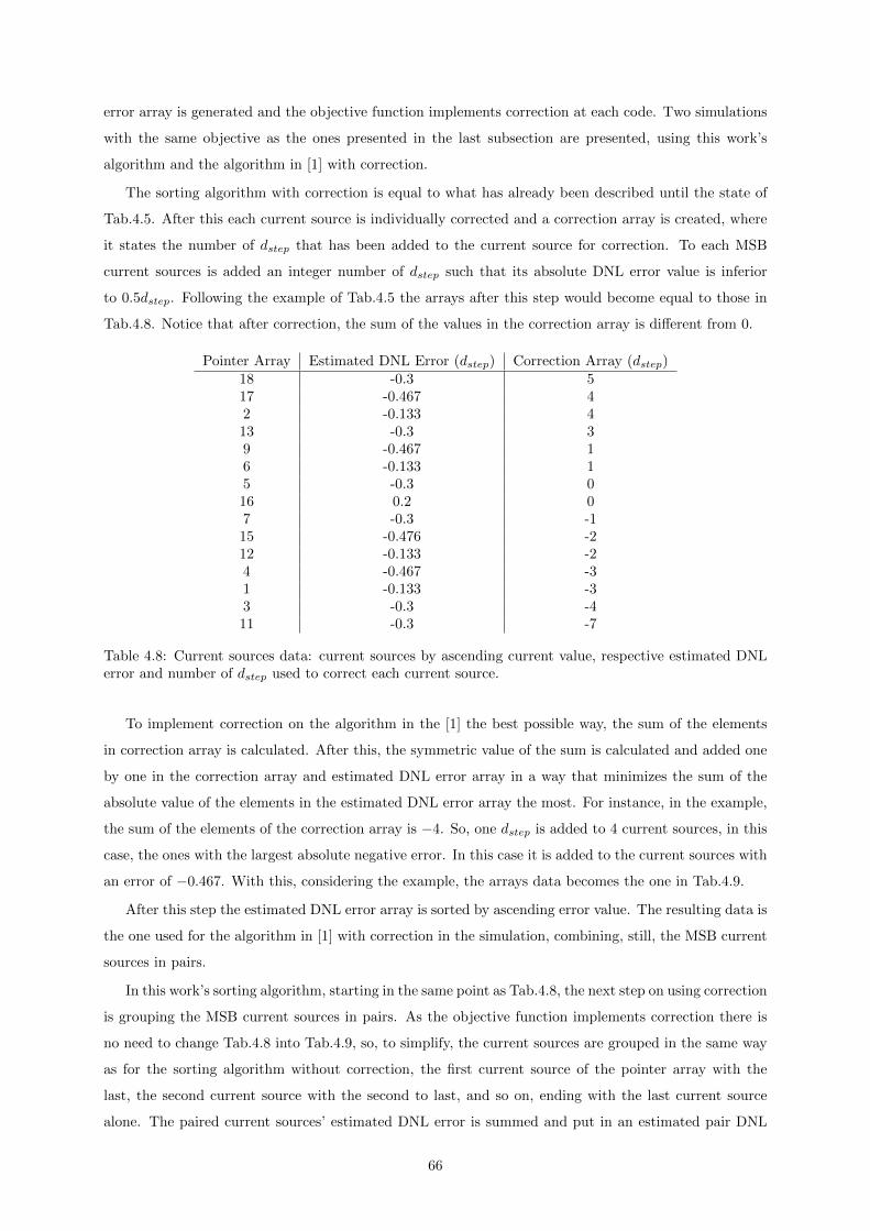
error array is generated and the objective function implements correction at each code. Two simulations
with the same objective as the ones presented in the last subsection are presented, using this work’s
algorithm and the algorithm in [1] with correction.
The sorting algorithm with correction is equal to what has already been described until the state of
Tab.4.5. After this each current source is individually corrected and a correction array is created, where
it states the number of dstep that has been added to the current source for correction. To each MSB
current sources is added an integer number of dstep such that its absolute DNL error value is inferior
to 0.5dstep. Following the example of Tab.4.5 the arrays after this step would become equal to those in
Tab.4.8. Notice that after correction, the sum of the values in the correction array is different from 0.
Pointer Array Estimated DNL Error (dstep) Correction Array (dstep)18 -0.3 517 -0.467 42 -0.133 413 -0.3 39 -0.467 16 -0.133 15 -0.3 016 0.2 07 -0.3 -115 -0.476 -212 -0.133 -24 -0.467 -31 -0.133 -33 -0.3 -411 -0.3 -7
Table 4.8: Current sources data: current sources by ascending current value, respective estimated DNLerror and number of dstep used to correct each current source.
To implement correction on the algorithm in the [1] the best possible way, the sum of the elements
in correction array is calculated. After this, the symmetric value of the sum is calculated and added one
by one in the correction array and estimated DNL error array in a way that minimizes the sum of the
absolute value of the elements in the estimated DNL error array the most. For instance, in the example,
the sum of the elements of the correction array is −4. So, one dstep is added to 4 current sources, in this
case, the ones with the largest absolute negative error. In this case it is added to the current sources with
an error of −0.467. With this, considering the example, the arrays data becomes the one in Tab.4.9.
After this step the estimated DNL error array is sorted by ascending error value. The resulting data is
the one used for the algorithm in [1] with correction in the simulation, combining, still, the MSB current
sources in pairs.
In this work’s sorting algorithm, starting in the same point as Tab.4.8, the next step on using correction
is grouping the MSB current sources in pairs. As the objective function implements correction there is
no need to change Tab.4.8 into Tab.4.9, so, to simplify, the current sources are grouped in the same way
as for the sorting algorithm without correction, the first current source of the pointer array with the
last, the second current source with the second to last, and so on, ending with the last current source
alone. The paired current sources’ estimated DNL error is summed and put in an estimated pair DNL
66
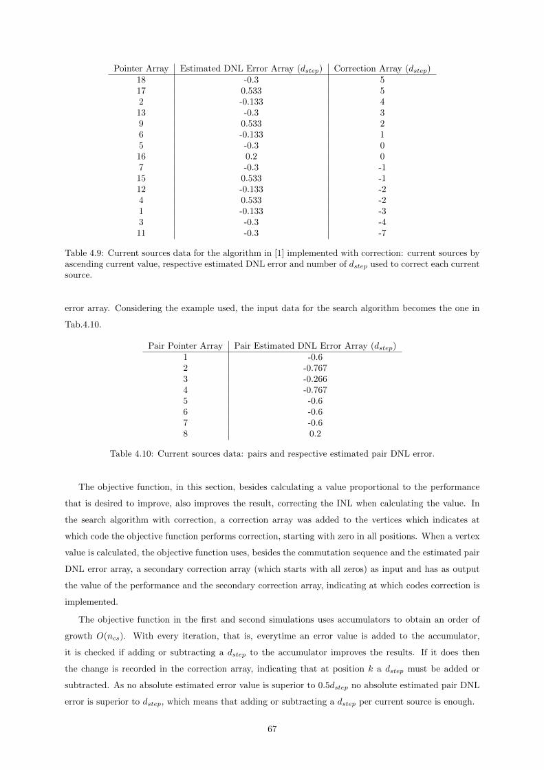
Pointer Array Estimated DNL Error Array (dstep) Correction Array (dstep)18 -0.3 517 0.533 52 -0.133 413 -0.3 39 0.533 26 -0.133 15 -0.3 016 0.2 07 -0.3 -115 0.533 -112 -0.133 -24 0.533 -21 -0.133 -33 -0.3 -411 -0.3 -7
Table 4.9: Current sources data for the algorithm in [1] implemented with correction: current sources byascending current value, respective estimated DNL error and number of dstep used to correct each currentsource.
error array. Considering the example used, the input data for the search algorithm becomes the one in
Tab.4.10.
Pair Pointer Array Pair Estimated DNL Error Array (dstep)1 -0.62 -0.7673 -0.2664 -0.7675 -0.66 -0.67 -0.68 0.2
Table 4.10: Current sources data: pairs and respective estimated pair DNL error.
The objective function, in this section, besides calculating a value proportional to the performance
that is desired to improve, also improves the result, correcting the INL when calculating the value. In
the search algorithm with correction, a correction array was added to the vertices which indicates at
which code the objective function performs correction, starting with zero in all positions. When a vertex
value is calculated, the objective function uses, besides the commutation sequence and the estimated pair
DNL error array, a secondary correction array (which starts with all zeros) as input and has as output
the value of the performance and the secondary correction array, indicating at which codes correction is
implemented.
The objective function in the first and second simulations uses accumulators to obtain an order of
growth O(ncs). With every iteration, that is, everytime an error value is added to the accumulator,
it is checked if adding or subtracting a dstep to the accumulator improves the results. If it does then
the change is recorded in the correction array, indicating that at position k a dstep must be added or
subtracted. As no absolute estimated error value is superior to 0.5dstep no absolute estimated pair DNL
error is superior to dstep, which means that adding or subtracting a dstep per current source is enough.
67
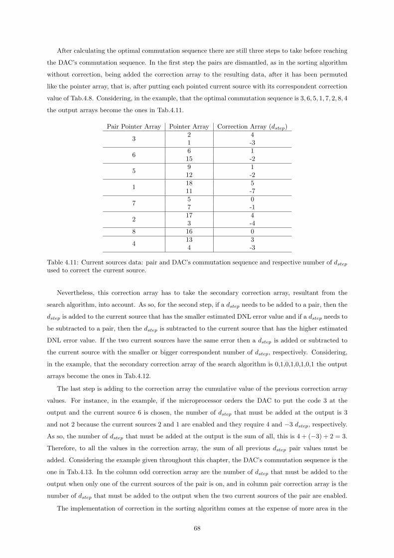
After calculating the optimal commutation sequence there are still three steps to take before reaching
the DAC’s commutation sequence. In the first step the pairs are dismantled, as in the sorting algorithm
without correction, being added the correction array to the resulting data, after it has been permuted
like the pointer array, that is, after putting each pointed current source with its correspondent correction
value of Tab.4.8. Considering, in the example, that the optimal commutation sequence is 3, 6, 5, 1, 7, 2, 8, 4
the output arrays become the ones in Tab.4.11.
Pair Pointer Array Pointer Array Correction Array (dstep)
32 41 -3
66 115 -2
59 112 -2
118 511 -7
75 07 -1
217 43 -4
8 16 0
413 34 -3
Table 4.11: Current sources data: pair and DAC’s commutation sequence and respective number of dstepused to correct the current source.
Nevertheless, this correction array has to take the secondary correction array, resultant from the
search algorithm, into account. As so, for the second step, if a dstep needs to be added to a pair, then the
dstep is added to the current source that has the smaller estimated DNL error value and if a dstep needs to
be subtracted to a pair, then the dstep is subtracted to the current source that has the higher estimated
DNL error value. If the two current sources have the same error then a dstep is added or subtracted to
the current source with the smaller or bigger correspondent number of dstep, respectively. Considering,
in the example, that the secondary correction array of the search algorithm is 0,1,0,1,0,1,0,1 the output
arrays become the ones in Tab.4.12.
The last step is adding to the correction array the cumulative value of the previous correction array
values. For instance, in the example, if the microprocessor orders the DAC to put the code 3 at the
output and the current source 6 is chosen, the number of dstep that must be added at the output is 3
and not 2 because the current sources 2 and 1 are enabled and they require 4 and −3 dstep, respectively.
As so, the number of dstep that must be added at the output is the sum of all, this is 4 + (−3) + 2 = 3.
Therefore, to all the values in the correction array, the sum of all previous dstep pair values must be
added. Considering the example given throughout this chapter, the DAC’s commutation sequence is the
one in Tab.4.13. In the column odd correction array are the number of dstep that must be added to the
output when only one of the current sources of the pair is on, and in column pair correction array is the
number of dstep that must be added to the output when the two current sources of the pair are enabled.
The implementation of correction in the sorting algorithm comes at the expense of more area in the
68
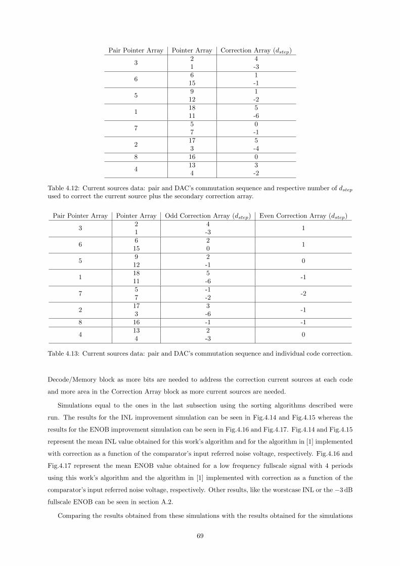
Pair Pointer Array Pointer Array Correction Array (dstep)
32 41 -3
66 115 -1
59 112 -2
118 511 -6
75 07 -1
217 53 -4
8 16 0
413 34 -2
Table 4.12: Current sources data: pair and DAC’s commutation sequence and respective number of dstepused to correct the current source plus the secondary correction array.
Pair Pointer Array Pointer Array Odd Correction Array (dstep) Even Correction Array (dstep)
32 4
11 -3
66 2
115 0
59 2
012 -1
118 5
-111 -6
75 -1
-27 -2
217 3
-13 -6
8 16 -1 -1
413 2
04 -3
Table 4.13: Current sources data: pair and DAC’s commutation sequence and individual code correction.
Decode/Memory block as more bits are needed to address the correction current sources at each code
and more area in the Correction Array block as more current sources are needed.
Simulations equal to the ones in the last subsection using the sorting algorithms described were
run. The results for the INL improvement simulation can be seen in Fig.4.14 and Fig.4.15 whereas the
results for the ENOB improvement simulation can be seen in Fig.4.16 and Fig.4.17. Fig.4.14 and Fig.4.15
represent the mean INL value obtained for this work’s algorithm and for the algorithm in [1] implemented
with correction as a function of the comparator’s input referred noise voltage, respectively. Fig.4.16 and
Fig.4.17 represent the mean ENOB value obtained for a low frequency fullscale signal with 4 periods
using this work’s algorithm and the algorithm in [1] implemented with correction as a function of the
comparator’s input referred noise voltage, respectively. Other results, like the worstcase INL or the −3 dB
fullscale ENOB can be seen in section A.2.
Comparing the results obtained from these simulations with the results obtained for the simulations
69
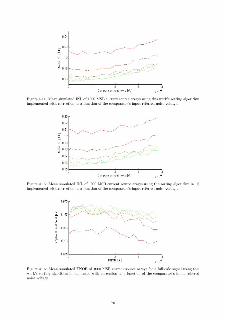
Figure 4.14: Mean simulated INL of 1000 MSB current source arrays using this work’s sorting algorithmimplemented with correction as a function of the comparator’s input referred noise voltage.
Figure 4.15: Mean simulated INL of 1000 MSB current source arrays using the sorting algorithm in [1]implemented with correction as a function of the comparator’s input referred noise voltage.
Figure 4.16: Mean simulated ENOB of 1000 MSB current source arrays for a fullscale signal using thiswork’s sorting algorithm implemented with correction as a function of the comparator’s input referrednoise voltage.
70
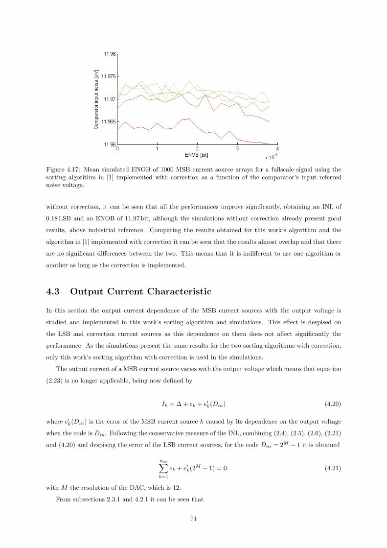
Figure 4.17: Mean simulated ENOB of 1000 MSB current source arrays for a fullscale signal using thesorting algorithm in [1] implemented with correction as a function of the comparator’s input referrednoise voltage.
without correction, it can be seen that all the performances improve significantly, obtaining an INL of
0.18 LSB and an ENOB of 11.97 bit, although the simulations without correction already present good
results, above industrial reference. Comparing the results obtained for this work’s algorithm and the
algorithm in [1] implemented with correction it can be seen that the results almost overlap and that there
are no significant differences between the two. This means that it is indifferent to use one algorithm or
another as long as the correction is implemented.
4.3 Output Current Characteristic
In this section the output current dependence of the MSB current sources with the output voltage is
studied and implemented in this work’s sorting algorithm and simulations. This effect is despised on
the LSB and correction current sources as this dependence on them does not affect significantly the
performance. As the simulations present the same results for the two sorting algorithms with correction,
only this work’s sorting algorithm with correction is used in the simulations.
The output current of a MSB current source varies with the output voltage which means that equation
(2.23) is no longer applicable, being now defined by
Ik = ∆ + ek + e′k(Din) (4.20)
where e′k(Din) is the error of the MSB current source k caused by its dependence on the output voltage
when the code is Din. Following the conservative measure of the INL, combining (2.4), (2.5), (2.6), (2.21)
and (4.20) and despising the error of the LSB current sources, for the code Din = 2M − 1 it is obtained
ncs∑k=1
ek + e′k(2M − 1) = 0. (4.21)
with M the resolution of the DAC, which is 12.
From subsections 2.3.1 and 4.2.1 it can be seen that
71
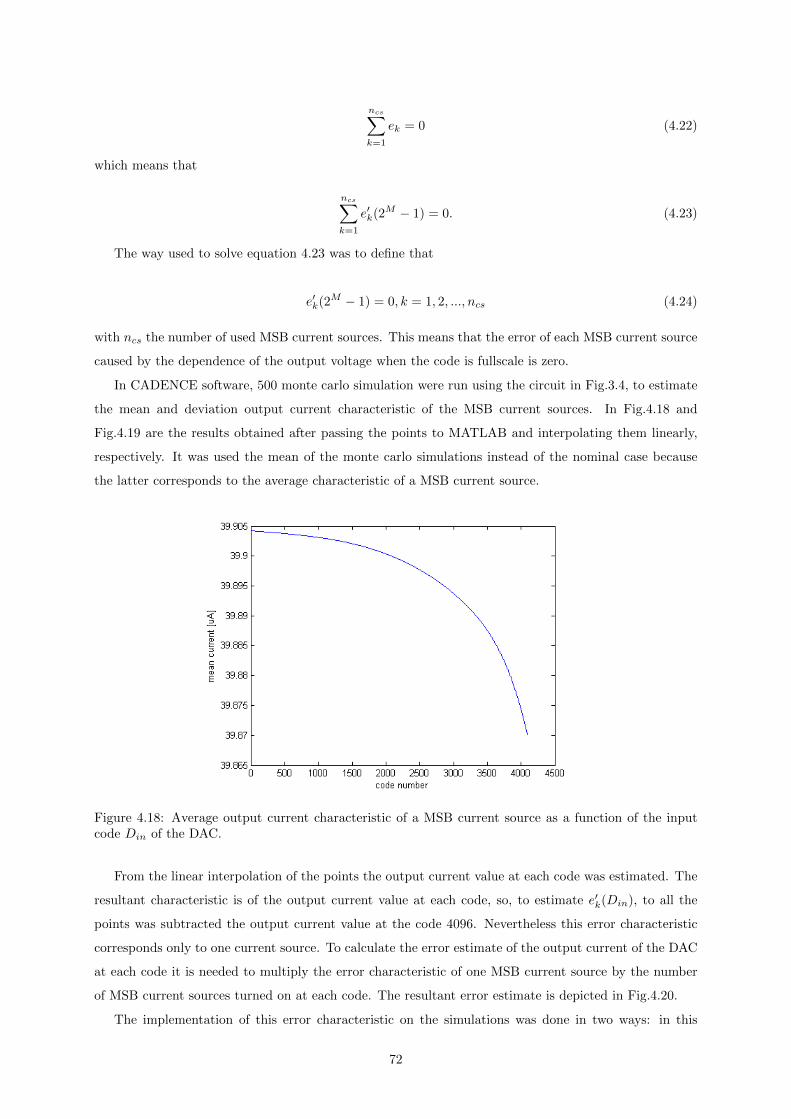
ncs∑k=1
ek = 0 (4.22)
which means that
ncs∑k=1
e′k(2M − 1) = 0. (4.23)
The way used to solve equation 4.23 was to define that
e′k(2M − 1) = 0, k = 1, 2, ..., ncs (4.24)
with ncs the number of used MSB current sources. This means that the error of each MSB current source
caused by the dependence of the output voltage when the code is fullscale is zero.
In CADENCE software, 500 monte carlo simulation were run using the circuit in Fig.3.4, to estimate
the mean and deviation output current characteristic of the MSB current sources. In Fig.4.18 and
Fig.4.19 are the results obtained after passing the points to MATLAB and interpolating them linearly,
respectively. It was used the mean of the monte carlo simulations instead of the nominal case because
the latter corresponds to the average characteristic of a MSB current source.
Figure 4.18: Average output current characteristic of a MSB current source as a function of the inputcode Din of the DAC.
From the linear interpolation of the points the output current value at each code was estimated. The
resultant characteristic is of the output current value at each code, so, to estimate e′k(Din), to all the
points was subtracted the output current value at the code 4096. Nevertheless this error characteristic
corresponds only to one current source. To calculate the error estimate of the output current of the DAC
at each code it is needed to multiply the error characteristic of one MSB current source by the number
of MSB current sources turned on at each code. The resultant error estimate is depicted in Fig.4.20.
The implementation of this error characteristic on the simulations was done in two ways: in this
72
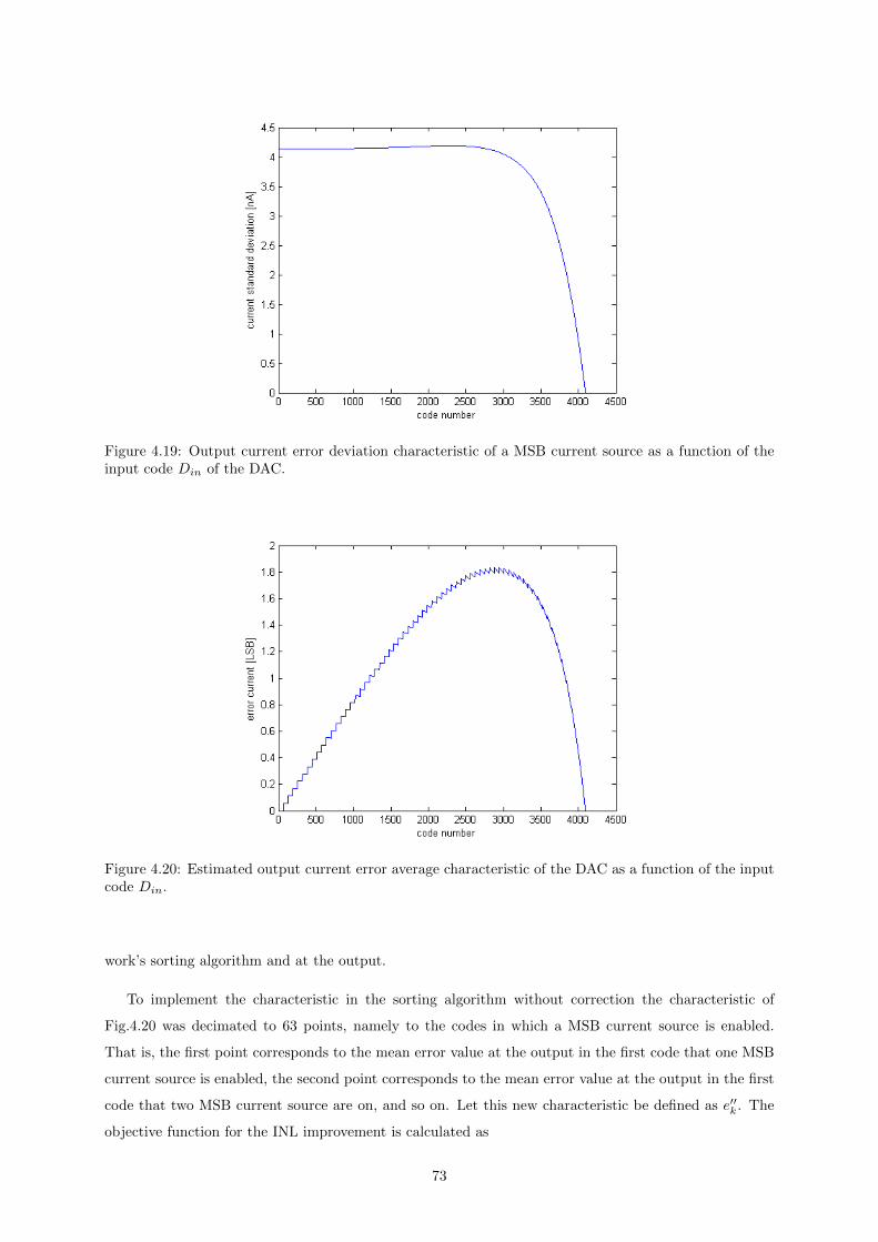
Figure 4.19: Output current error deviation characteristic of a MSB current source as a function of theinput code Din of the DAC.
Figure 4.20: Estimated output current error average characteristic of the DAC as a function of the inputcode Din.
work’s sorting algorithm and at the output.
To implement the characteristic in the sorting algorithm without correction the characteristic of
Fig.4.20 was decimated to 63 points, namely to the codes in which a MSB current source is enabled.
That is, the first point corresponds to the mean error value at the output in the first code that one MSB
current source is enabled, the second point corresponds to the mean error value at the output in the first
code that two MSB current source are on, and so on. Let this new characteristic be defined as e′′k . The
objective function for the INL improvement is calculated as
73
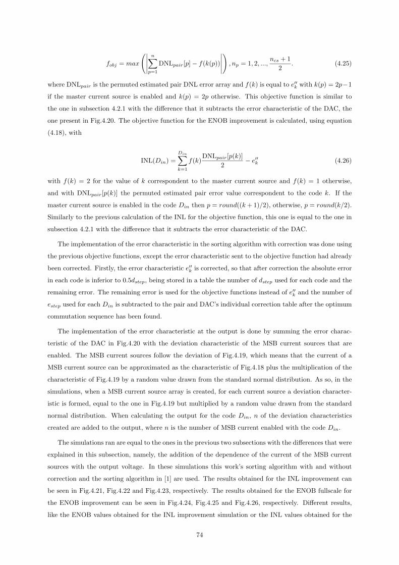
fobj = max
(∣∣∣∣∣n∑p=1
DNLpair[p]− f(k(p))
∣∣∣∣∣), np = 1, 2, ...,
ncs + 1
2. (4.25)
where DNLpair is the permuted estimated pair DNL error array and f(k) is equal to e′′k with k(p) = 2p−1
if the master current source is enabled and k(p) = 2p otherwise. This objective function is similar to
the one in subsection 4.2.1 with the difference that it subtracts the error characteristic of the DAC, the
one present in Fig.4.20. The objective function for the ENOB improvement is calculated, using equation
(4.18), with
INL(Din) =
Din∑k=1
f(k)DNLpair[p(k)]
2− e′′k (4.26)
with f(k) = 2 for the value of k correspondent to the master current source and f(k) = 1 otherwise,
and with DNLpair[p(k)] the permuted estimated pair error value correspondent to the code k. If the
master current source is enabled in the code Din then p = round((k+ 1)/2), otherwise, p = round(k/2).
Similarly to the previous calculation of the INL for the objective function, this one is equal to the one in
subsection 4.2.1 with the difference that it subtracts the error characteristic of the DAC.
The implementation of the error characteristic in the sorting algorithm with correction was done using
the previous objective functions, except the error characteristic sent to the objective function had already
been corrected. Firstly, the error characteristic e′′k is corrected, so that after correction the absolute error
in each code is inferior to 0.5dstep, being stored in a table the number of dstep used for each code and the
remaining error. The remaining error is used for the objective functions instead of e′′k and the number of
estep used for each Din is subtracted to the pair and DAC’s individual correction table after the optimum
commutation sequence has been found.
The implementation of the error characteristic at the output is done by summing the error charac-
teristic of the DAC in Fig.4.20 with the deviation characteristic of the MSB current sources that are
enabled. The MSB current sources follow the deviation of Fig.4.19, which means that the current of a
MSB current source can be approximated as the characteristic of Fig.4.18 plus the multiplication of the
characteristic of Fig.4.19 by a random value drawn from the standard normal distribution. As so, in the
simulations, when a MSB current source array is created, for each current source a deviation character-
istic is formed, equal to the one in Fig.4.19 but multiplied by a random value drawn from the standard
normal distribution. When calculating the output for the code Din, n of the deviation characteristics
created are added to the output, where n is the number of MSB current enabled with the code Din.
The simulations ran are equal to the ones in the previous two subsections with the differences that were
explained in this subsection, namely, the addition of the dependence of the current of the MSB current
sources with the output voltage. In these simulations this work’s sorting algorithm with and without
correction and the sorting algorithm in [1] are used. The results obtained for the INL improvement can
be seen in Fig.4.21, Fig.4.22 and Fig.4.23, respectively. The results obtained for the ENOB fullscale for
the ENOB improvement can be seen in Fig.4.24, Fig.4.25 and Fig.4.26, respectively. Different results,
like the ENOB values obtained for the INL improvement simulation or the INL values obtained for the
74
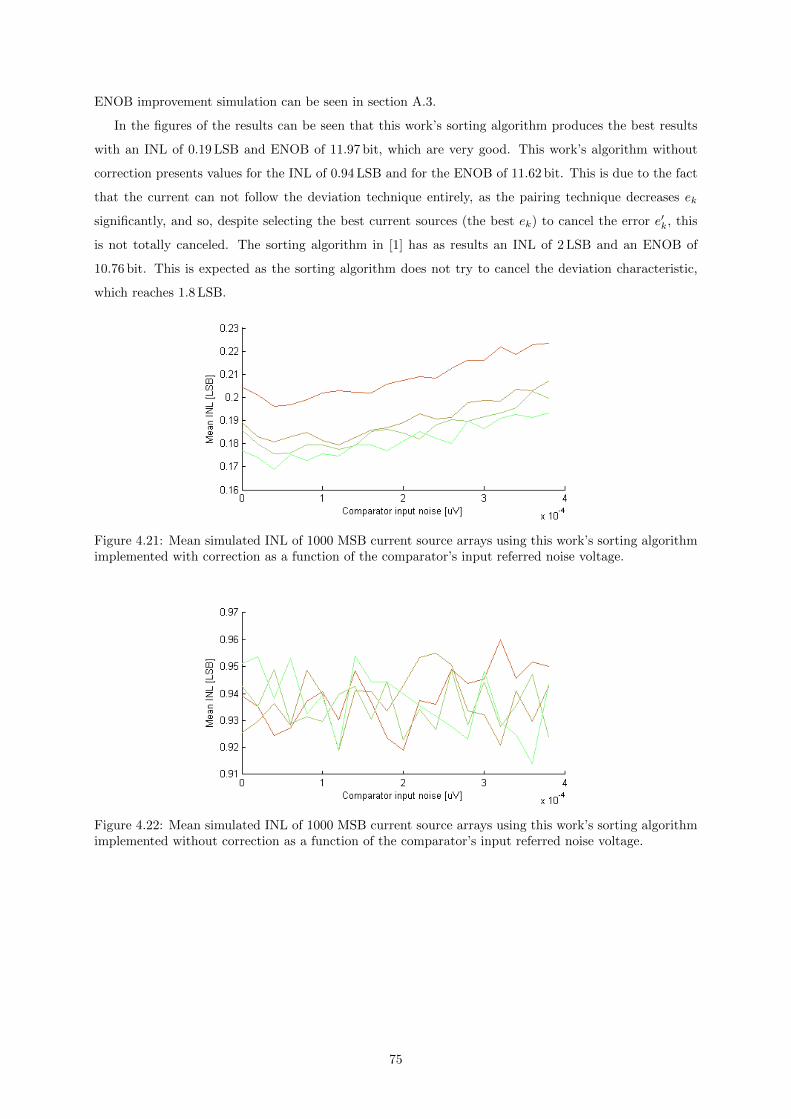
ENOB improvement simulation can be seen in section A.3.
In the figures of the results can be seen that this work’s sorting algorithm produces the best results
with an INL of 0.19 LSB and ENOB of 11.97 bit, which are very good. This work’s algorithm without
correction presents values for the INL of 0.94 LSB and for the ENOB of 11.62 bit. This is due to the fact
that the current can not follow the deviation technique entirely, as the pairing technique decreases ek
significantly, and so, despite selecting the best current sources (the best ek) to cancel the error e′k, this
is not totally canceled. The sorting algorithm in [1] has as results an INL of 2 LSB and an ENOB of
10.76 bit. This is expected as the sorting algorithm does not try to cancel the deviation characteristic,
which reaches 1.8 LSB.
Figure 4.21: Mean simulated INL of 1000 MSB current source arrays using this work’s sorting algorithmimplemented with correction as a function of the comparator’s input referred noise voltage.
Figure 4.22: Mean simulated INL of 1000 MSB current source arrays using this work’s sorting algorithmimplemented without correction as a function of the comparator’s input referred noise voltage.
75
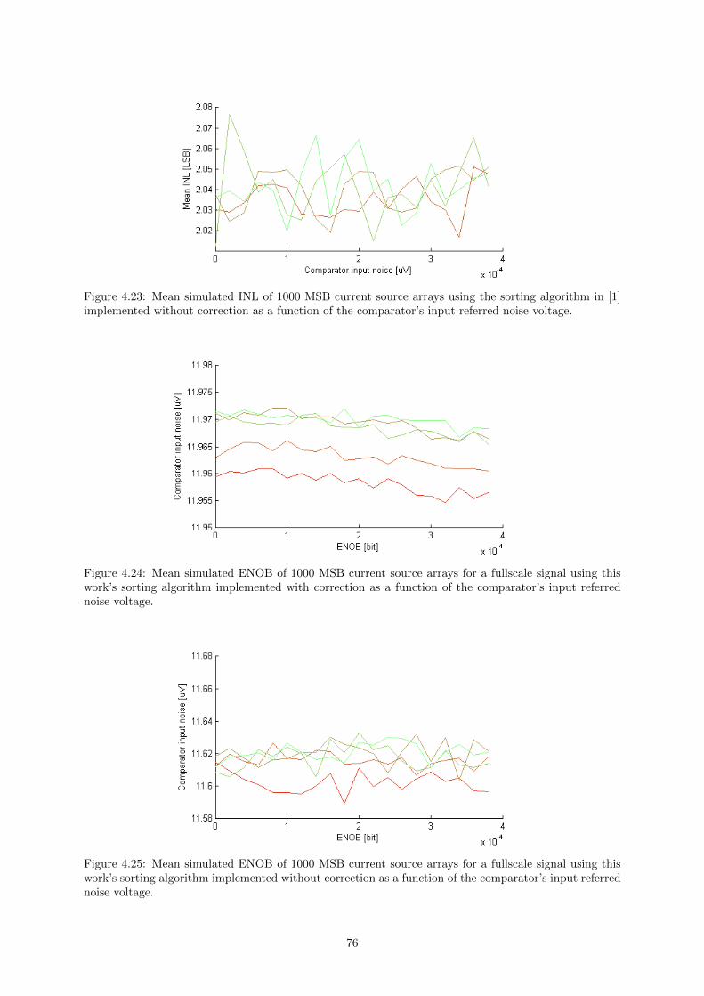
Figure 4.23: Mean simulated INL of 1000 MSB current source arrays using the sorting algorithm in [1]implemented without correction as a function of the comparator’s input referred noise voltage.
Figure 4.24: Mean simulated ENOB of 1000 MSB current source arrays for a fullscale signal using thiswork’s sorting algorithm implemented with correction as a function of the comparator’s input referrednoise voltage.
Figure 4.25: Mean simulated ENOB of 1000 MSB current source arrays for a fullscale signal using thiswork’s sorting algorithm implemented without correction as a function of the comparator’s input referrednoise voltage.
76
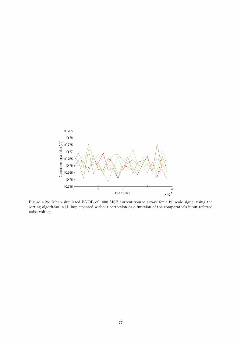
Figure 4.26: Mean simulated ENOB of 1000 MSB current source arrays for a fullscale signal using thesorting algorithm in [1] implemented without correction as a function of the comparator’s input referrednoise voltage.
77

78
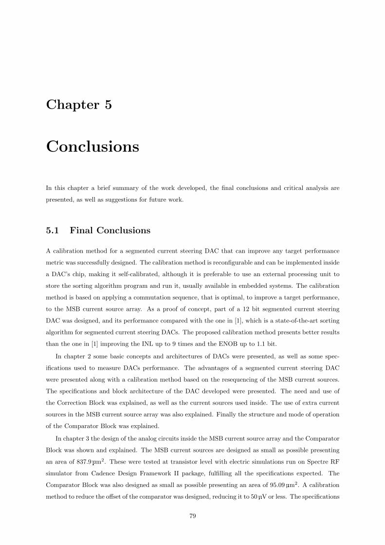
Chapter 5
Conclusions
In this chapter a brief summary of the work developed, the final conclusions and critical analysis are
presented, as well as suggestions for future work.
5.1 Final Conclusions
A calibration method for a segmented current steering DAC that can improve any target performance
metric was successfully designed. The calibration method is reconfigurable and can be implemented inside
a DAC’s chip, making it self-calibrated, although it is preferable to use an external processing unit to
store the sorting algorithm program and run it, usually available in embedded systems. The calibration
method is based on applying a commutation sequence, that is optimal, to improve a target performance,
to the MSB current source array. As a proof of concept, part of a 12 bit segmented current steering
DAC was designed, and its performance compared with the one in [1], which is a state-of-the-art sorting
algorithm for segmented current steering DACs. The proposed calibration method presents better results
than the one in [1] improving the INL up to 9 times and the ENOB up to 1.1 bit.
In chapter 2 some basic concepts and architectures of DACs were presented, as well as some spec-
ifications used to measure DACs performance. The advantages of a segmented current steering DAC
were presented along with a calibration method based on the resequencing of the MSB current sources.
The specifications and block architecture of the DAC developed were presented. The need and use of
the Correction Block was explained, as well as the current sources used inside. The use of extra current
sources in the MSB current source array was also explained. Finally the structure and mode of operation
of the Comparator Block was explained.
In chapter 3 the design of the analog circuits inside the MSB current source array and the Comparator
Block was shown and explained. The MSB current sources are designed as small as possible presenting
an area of 837.9µm2. These were tested at transistor level with electric simulations run on Spectre RF
simulator from Cadence Design Framework II package, fulfilling all the specifications expected. The
Comparator Block was also designed as small as possible presenting an area of 95.09 µm2. A calibration
method to reduce the offset of the comparator was designed, reducing it to 50µV or less. The specifications
79

for the Comparator Block were tested using the transistor level simulator referred above and a MATLAB
model, being fulfilled.
In chapter 4 the sorting algorithm developed in this work was presented, being explained how to
implement it with or without the use of output correction. The implementation of correction in the
sorting algorithm comes at the expense of more area in the Decode/Memory block as more bits are
needed to address the correction current sources at each code. The use of correction is advisable in
the case area is not a limiting specification or the calibration method without correction is not enough
to reach the specifications. Simulations using the specifications of the circuits developed were ran to
compare the developed sorting algorithm with the one in [1]. In the first simulation the sorting algorithm
was simulated without the use of correction and considering the current sources had infinite output
impedance. The results show that the INL improves from 0.64 LSB, value that is achieved by the sorting
algorithm in [1] to 0.3 LSB, value that is achieved by this work’s sorting algorithm. The second simulation
is done with the use of correction for both sorting algorithms and considering that the current sources
have infinite output impedance. The results for both the sorting algorithms almost overlap, achieving
an INL of 0.2 LSB, being, thus, irrelevant the sorting algorithm used, as long as correction is used. In
the third simulation this work’s sorting algorithm with and without the use of correction and the one
in [1] without correction were used, taking the finite output impedance obtained for the MSB current
sources into account. The results obtained for the INL were 2 LSB, 0.94 LSB and 0.19 LSB and for the
ENOB were 11.97 bit, 11.62 bit and 10.76 bit, respectively. The calibration method in [1] does not take
the deviation characteristic of the MSB current sources into account, so it is expected for its INL to
be high. The sorting algorithm of this work without correction does not achieve very good results in
this simulation as it cannot follow the deviation characteristic. This is due to the pairing technique that
decreases the DNL characteristic of the DAC significantly. The ENOB simulations are done considering
that the input signals are low frequency, meaning that high frequency effects impacting the conversion
were not studied.
5.2 Future Work
Following the conclusions drawn above, some topics are suggested in order to complement or continue
the work developed in this thesis:
• Design the Decode/Memory, Control Unit and LSB and Correction Array blocks, for the sorting
algorithm with correction and without correction in order to verify the total area occupied by the
DAC in the two cases.
• Test the dynamic behavior of the DAC, implementing high frequency effects on the simulations.
• Develop layouts of the DAC for the sorting algorithm with and without correction and extract its
view in order to simulate and guarantee the specifications and improvements.
• Implement the DACs in silicon and test them for the sorting algorithm with and without correction,
using an external processing unit.
80
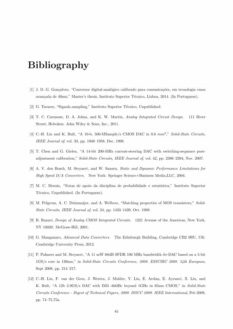
Bibliography
[1] J. D. G. Goncalves, “Conversor digital-analogico calibrado para comunicacoes, em tecnologia cmos
avancada de 40nm,” Master’s thesis, Instituto Superior Tecnico, Lisboa, 2014. (In Portuguese).
[2] G. Tavares, “Signals sampling,” Instituto Superior Tecnico, Unpublished.
[3] T. C. Carusone, D. A. Johns, and K. W. Martin, Analog Integrated Circuit Design. 111 River
Street, Hoboken: John Wiley & Sons, Inc., 2011.
[4] C.-H. Lin and K. Bult, “A 10-b, 500-MSample/s CMOS DAC in 0.6 mm2,” Solid-State Circuits,
IEEE Journal of, vol. 33, pp. 1948–1958, Dec. 1998.
[5] T. Chen and G. Gielen, “A 14-bit 200-MHz current-steering DAC with switching-sequence post-
adjustment calibration,” Solid-State Circuits, IEEE Journal of, vol. 42, pp. 2386–2394, Nov. 2007.
[6] A. V. den Bosch, M. Steyaert, and W. Sansen, Static and Dynamic Performance Limitations for
High Speed D/A Converters. New York: Springer Science+Business Media,LLC, 2004.
[7] M. C. Morais, “Notas de apoio da disciplina de probabilidade e estatıstica,” Instituto Superior
Tecnico, Unpublished. (In Portuguese).
[8] M. Pelgrom, A. C. Duinmaijer, and A. Welbers, “Matching properties of MOS transistors,” Solid-
State Circuits, IEEE Journal of, vol. 24, pp. 1433–1439, Oct. 1989.
[9] B. Razavi, Design of Analog CMOS Integrated Circuits. 1221 Avenue of the Americas, New York,
NY 10020: McGraw-Hill, 2001.
[10] G. Manganaro, Advanced Data Converters. The Edinburgh Building, Cambridge CB2 8RU, UK:
Cambridge University Press, 2012.
[11] P. Palmers and M. Steyaert, “A 11 mW 68dB SFDR 100 MHz bandwidth δσ-DAC based on a 5-bit
1GS/s core in 130nm,” in Solid-State Circuits Conference, 2008. ESSCIRC 2008. 34th European,
Sept 2008, pp. 214–217.
[12] C.-H. Lin, F. van der Goes, J. Westra, J. Mulder, Y. Lin, E. Arslan, E. Ayranci, X. Liu, and
K. Bult, “A 12b 2.9GS/s DAC with IM3 -60dBc beyond 1GHz in 65nm CMOS,” in Solid-State
Circuits Conference - Digest of Technical Papers, 2009. ISSCC 2009. IEEE International, Feb 2009,
pp. 74–75,75a.
81

[13] M. van Elzakker, E. van Tuijl, P. Geraedts, D. Schinkel, E. Klumperink, and B. Nauta, “A 10-bit
Charge-Redistribution ADC consuming 1.9µW at 1 MS/s,” Solid-State Circuits, IEEE Journal of,
vol. 45, no. 5, pp. 1007–1015, May 2010.
[14] R. Sedgewick and K. Wayne, Algorithms in C. 501 Boylston Street, Suite 900, Boston, MA 02116:
Pearson Education, Inc., 2011.
[15] T. Sepke, P. Holloway, C. Sodini, and H.-S. Lee, “Noise analysis for comparator-based circuits,”
Circuits and Systems I: Regular Papers, IEEE Transactions on, vol. 56, no. 3, pp. 541–553, March
2009.
[16] A. Ayed, H. Ghariani, and M. Samet, “Design and optimization of CMOS OTA with gm/Id method-
ology using EKV model for RF frequency synthesizer application.” in Electronics, Circuits and Sys-
tems, 2005. ICECS 2005. 12th IEEE International Conference on, Dec 2005, pp. 1–5.
[17] B. Razavi, “The StrongARM Latch [A Circuit for All Seasons],” Solid-State Circuits Magazine,
IEEE, vol. 7, no. 2, pp. 12–17, Spring 2015.
[18] P. Nuzzo, F. De Bernardinis, P. Terreni, and G. Van der Plas, “Noise Analysis of Regenerative
Comparators for Reconfigurable ADC Architectures,” Circuits and Systems I: Regular Papers, IEEE
Transactions on, vol. 55, no. 6, pp. 1441–1454, July 2008.
[19] T. W. Judson, “Abstract algebra: Theory and applications,” Stephen F. Austin State University,
2012, Unpublished.
82
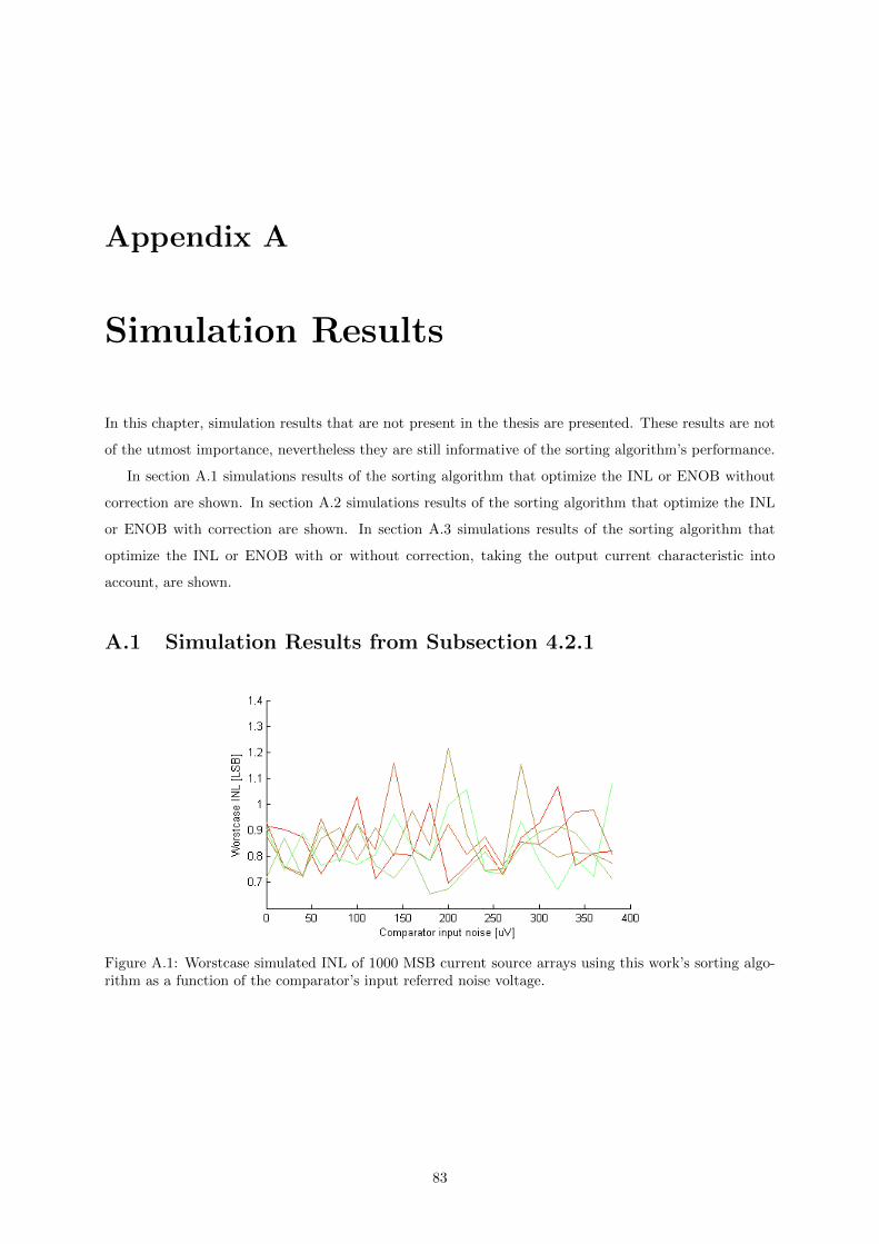
Appendix A
Simulation Results
In this chapter, simulation results that are not present in the thesis are presented. These results are not
of the utmost importance, nevertheless they are still informative of the sorting algorithm’s performance.
In section A.1 simulations results of the sorting algorithm that optimize the INL or ENOB without
correction are shown. In section A.2 simulations results of the sorting algorithm that optimize the INL
or ENOB with correction are shown. In section A.3 simulations results of the sorting algorithm that
optimize the INL or ENOB with or without correction, taking the output current characteristic into
account, are shown.
A.1 Simulation Results from Subsection 4.2.1
Figure A.1: Worstcase simulated INL of 1000 MSB current source arrays using this work’s sorting algo-rithm as a function of the comparator’s input referred noise voltage.
83
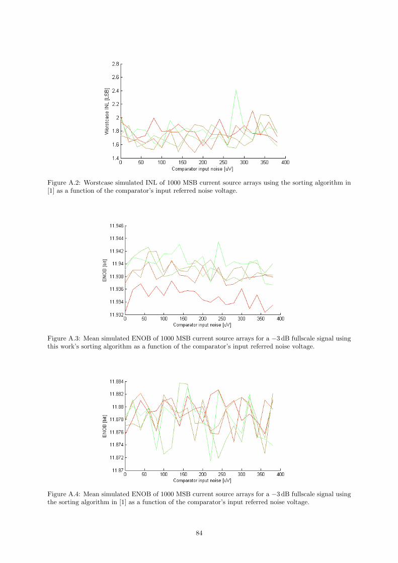
Figure A.2: Worstcase simulated INL of 1000 MSB current source arrays using the sorting algorithm in[1] as a function of the comparator’s input referred noise voltage.
Figure A.3: Mean simulated ENOB of 1000 MSB current source arrays for a −3 dB fullscale signal usingthis work’s sorting algorithm as a function of the comparator’s input referred noise voltage.
Figure A.4: Mean simulated ENOB of 1000 MSB current source arrays for a −3 dB fullscale signal usingthe sorting algorithm in [1] as a function of the comparator’s input referred noise voltage.
84
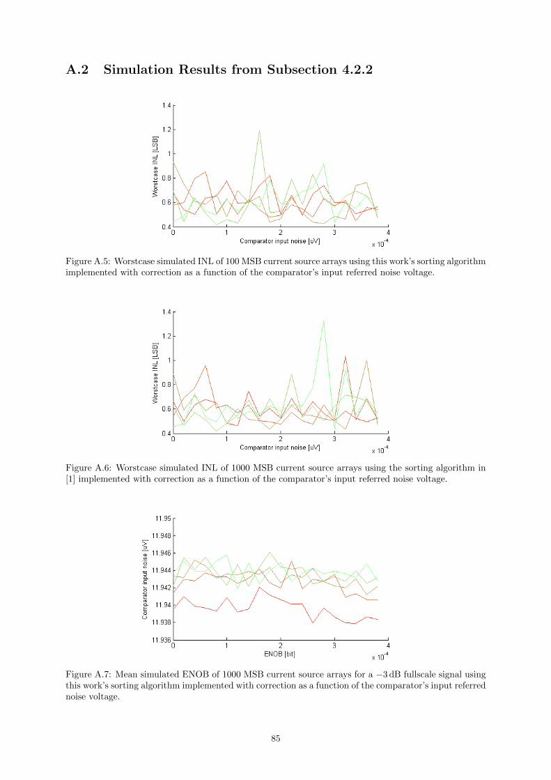
A.2 Simulation Results from Subsection 4.2.2
Figure A.5: Worstcase simulated INL of 100 MSB current source arrays using this work’s sorting algorithmimplemented with correction as a function of the comparator’s input referred noise voltage.
Figure A.6: Worstcase simulated INL of 1000 MSB current source arrays using the sorting algorithm in[1] implemented with correction as a function of the comparator’s input referred noise voltage.
Figure A.7: Mean simulated ENOB of 1000 MSB current source arrays for a −3 dB fullscale signal usingthis work’s sorting algorithm implemented with correction as a function of the comparator’s input referrednoise voltage.
85
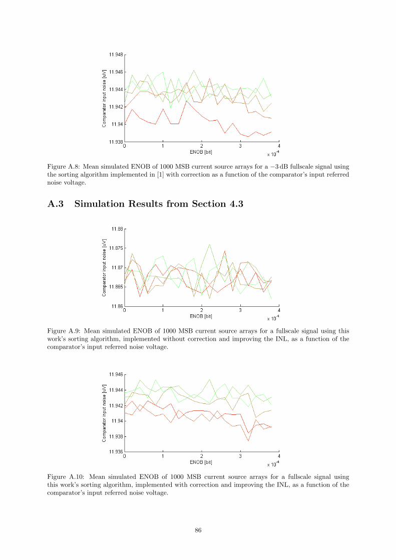
Figure A.8: Mean simulated ENOB of 1000 MSB current source arrays for a −3 dB fullscale signal usingthe sorting algorithm implemented in [1] with correction as a function of the comparator’s input referrednoise voltage.
A.3 Simulation Results from Section 4.3
Figure A.9: Mean simulated ENOB of 1000 MSB current source arrays for a fullscale signal using thiswork’s sorting algorithm, implemented without correction and improving the INL, as a function of thecomparator’s input referred noise voltage.
Figure A.10: Mean simulated ENOB of 1000 MSB current source arrays for a fullscale signal usingthis work’s sorting algorithm, implemented with correction and improving the INL, as a function of thecomparator’s input referred noise voltage.
86
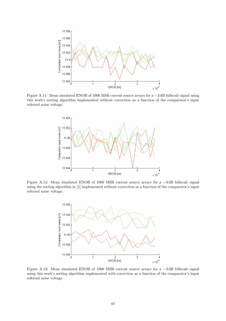
Figure A.11: Mean simulated ENOB of 1000 MSB current source arrays for a −3 dB fullscale signal usingthis work’s sorting algorithm implemented without correction as a function of the comparator’s inputreferred noise voltage.
Figure A.12: Mean simulated ENOB of 1000 MSB current source arrays for a −3 dB fullscale signalusing the sorting algorithm in [1] implemented without correction as a function of the comparator’s inputreferred noise voltage.
Figure A.13: Mean simulated ENOB of 1000 MSB current source arrays for a −3 dB fullscale signalusing this work’s sorting algorithm implemented with correction as a function of the comparator’s inputreferred noise voltage.
87
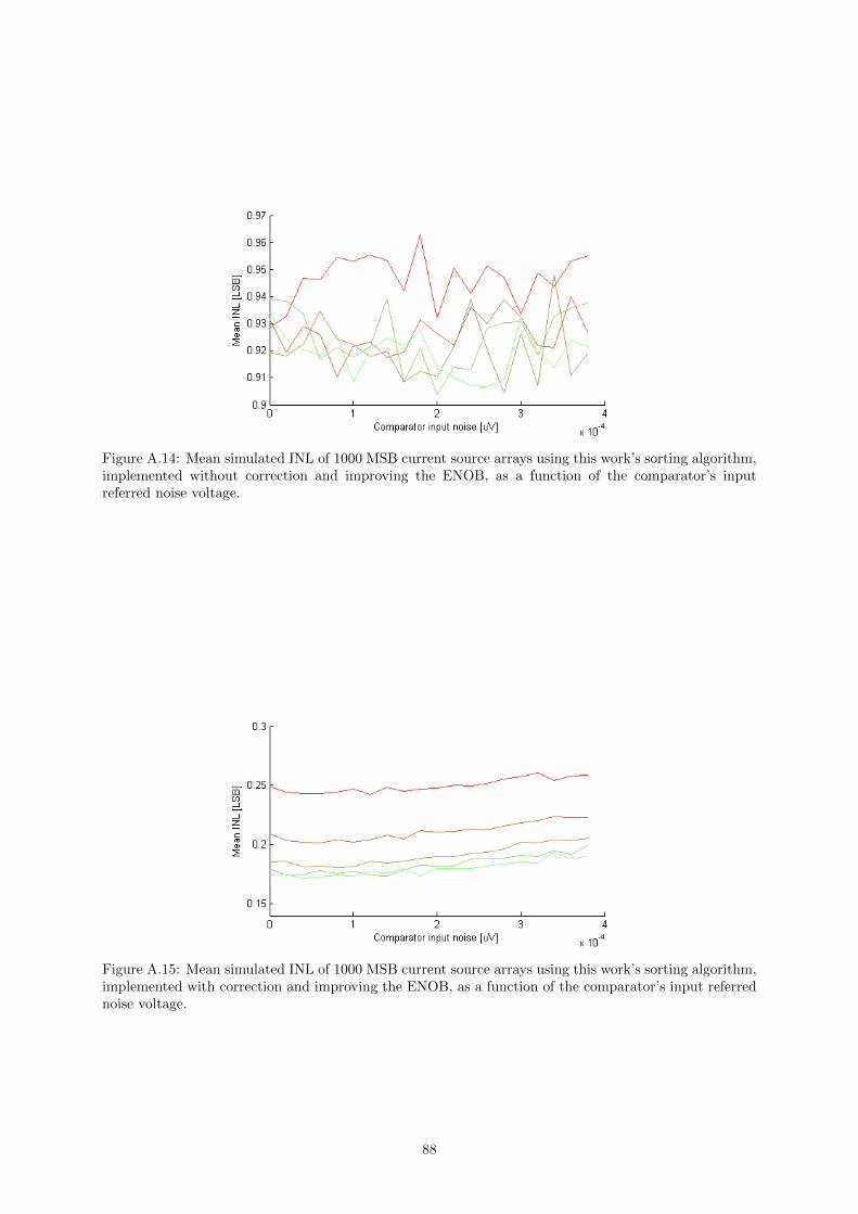
Figure A.14: Mean simulated INL of 1000 MSB current source arrays using this work’s sorting algorithm,implemented without correction and improving the ENOB, as a function of the comparator’s inputreferred noise voltage.
Figure A.15: Mean simulated INL of 1000 MSB current source arrays using this work’s sorting algorithm,implemented with correction and improving the ENOB, as a function of the comparator’s input referrednoise voltage.
88