Embed Size (px)
Citation preview

Reconfigurable, High Density, High Speed, Radiation Hardened FPGA Technology
MAPLD2009
S.Ramaswamy1, Leonard Rockett1, D. Bostedo1 Rajit Manohar2, Clinton W. Kelly, IV2, John Lofton Holt2, V. Ekanayake2, Dan Elftmann2
Ken LaBel3, Melanie Berg3 1BAE SYSTEMS, 9300 Wellington Road, Manassas, VA, 20110, USA2Achronix Semiconductor Corporation, 333 W. San Carlos Street, San Jose, CA, 95110, USA3NASA Goddard, 8800 Greenbelt Road, Greenbelt, MD, 20771, USA
&
&2
Agenda
RHFPGA Roadmap
RHFPGA Product Features
Achronix Technology Overview
BAE Radiation Hardened Process Technology Overview
RHFPGA Product Features
Summary
&3
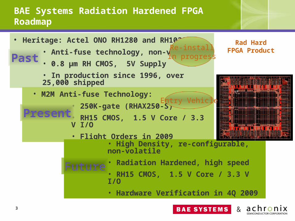
BAE Systems Radiation Hardened FPGA Roadmap
• Heritage: Actel ONO RH1280 and RH1020
• Anti-fuse technology, non-volatile
• 0.8 µm RH CMOS, 5V Supply
• In production since 1996, over 25,000 shipped
• M2M Anti-fuse Technology:
• 250K-gate (RHAX250-S)
• RH15 CMOS, 1.5 V Core / 3.3 V I/O
• Flight Orders in 2009
• High Density, re-configurable, non-volatile
• Radiation Hardened, high speed
• RH15 CMOS, 1.5 V Core / 3.3 V I/O
• Hardware Verification in 4Q 2009
Rad Hard FPGA Product
Past
Present
Future
Re-installin progress
Entry Vehicle
&4
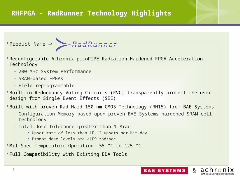
RHFPGA - RadRunner Technology Highlights
Product Name
Reconfigurable Achronix picoPIPE Radiation Hardened FPGA Acceleration Technology
– 200 MHz System Performance
– SRAM-based FPGAs
– Field reprogrammable Built-in Redundancy Voting Circuits (RVC) transparently protect the user design from Single Event
Effects (SEE)
Built with proven Rad Hard 150 nm CMOS Technology (RH15) from BAE Systems
– Configuration Memory based upon proven BAE Systems hardened SRAM cell technology
– Total-dose tolerance greater than 1 Mrad • Upset rate of less than 1E-12 upsets per bit-day
• Prompt dose levels are >1E9 rad/sec
Mil-Spec Temperature Operation -55 °C to 125 °C
Full Compatibility with Existing EDA Tools

&5
Achronix Company Overview
Privately held fabless semiconductor company founded in New York in 2004
Achronix received $34.4M Series A funding in January 2007
Completed $52.1M Series B funding in October 2008
Founders developed technology in 1998 at Cornell University
Headquartered in San Jose, CA
Partnerships with the world leading foundry TSMC, and numerous IP & EDA vendors
65 nm commercial FPGA silicon from TSMC completed Qualification and is currently shipping
Partnership with BAE Systems to develop RadHard FPGAs
Series of Patents protect key IP
Achronix Corporate Overview
&
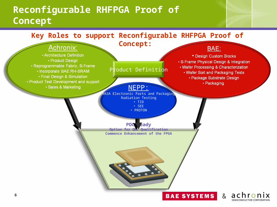
Reconfigurable RHFPGA Proof of Concept
6
POC ReadyOption for QML Qualification
Commence Enhancement of the FPGA
Key Roles to support Reconfigurable RHFPGA Proof of Concept:
NEPP:(NASA Electronic Parts and Packaging)
Radiation Testing• TID• SEE
• PROTON
Product Definition

&7
Achronix RHFPGA Technology

&8
Achronix Core Technology
Core contains ‘picoPIPE’ technology used for both logic and routing– You do not need to know the details in
order to benefit from this
Fully synchronous I/O ‘frame’ surrounds the core
picoPIPE technology is used to implement synchronous hardware – A design is input using a HDL such as
RTL
– The RTL does not need to be targeted to picoPIPE technology
Achronix FPGA
Globally-clockedlogic
‘frame’
picoPIPElogic core
Looks like a regular FPGA, but has approx 4x throughput

&9
Friday, April 21, 2023
D1 D Q
CLK
D Q
Globally clocked pipeline stage
Traditional Data Tokens
CLK
D1
Q1
Active edge Active edge
In globally-clocked logic, a data value at a clock edge can be considered as a “Data Token”
– Only valid data (data at a clock edge) is propagated
– Hence each register outputs a new Data Token (value) at every clock edge
Traditional FPGA
01Q1 Q2
1

&10
Friday, April 21, 2023
picoPIPE Data Tokens
Data 1
Data 0
Acknowledge
Data 1 Valid Data 1 Reset
Data 0 Valid Data 0 Reset
Acknowledge Valid
IDLE Acknowledge Data ResetData Valid IDLE Data Valid Acknowledge Data Reset IDLE
Acknowledge Reset
Acknowledge Valid
Acknowledge Reset
Phase
Data 0
Data 1
Acknowledge
picoPIPE pipeline stage
TxRx TxRx1
picoPIPE logic also communicates with Data Tokens– Each data token uses 2 signals
instead of 1– Data Token transfers use a four
phase handshake– Data validation (clock-like
functionality) is performed using acknowledge instead of a global clock
0
Achronix FPGA

&11
Friday, April 21, 2023
Pipelining Increases Throughput
Traditional FPGA Globally Clocked Logic is not balanced The clock rate must allow for the slowest
path in the entire clock domain Any combinatorial logic faster than the
slowest path (by definition, all remaining logic) waits for the slowest one to finish
Globally-clocked Logic
1.5
GH
z3
75
MH
z
Achronix FPGA Achronix technology allows fine-grained
pipelining Allows data rate to be much faster Pipelining also allows more data values in
flight Equates to faster throughput
Tra
ditio
nal
Ach
roni
x
picoPIPE Logic
0ps .67ns 1.3ns 2.0ns 2.7ns 3.3ns 4ns 4.7ns 5.3ns 6ns 6.7ns 7.3ns 8ns 8.7ns 9.3ns 10ns 10.7ns
D Q D QD Q
clk
1234
12345678910111213141516
&12
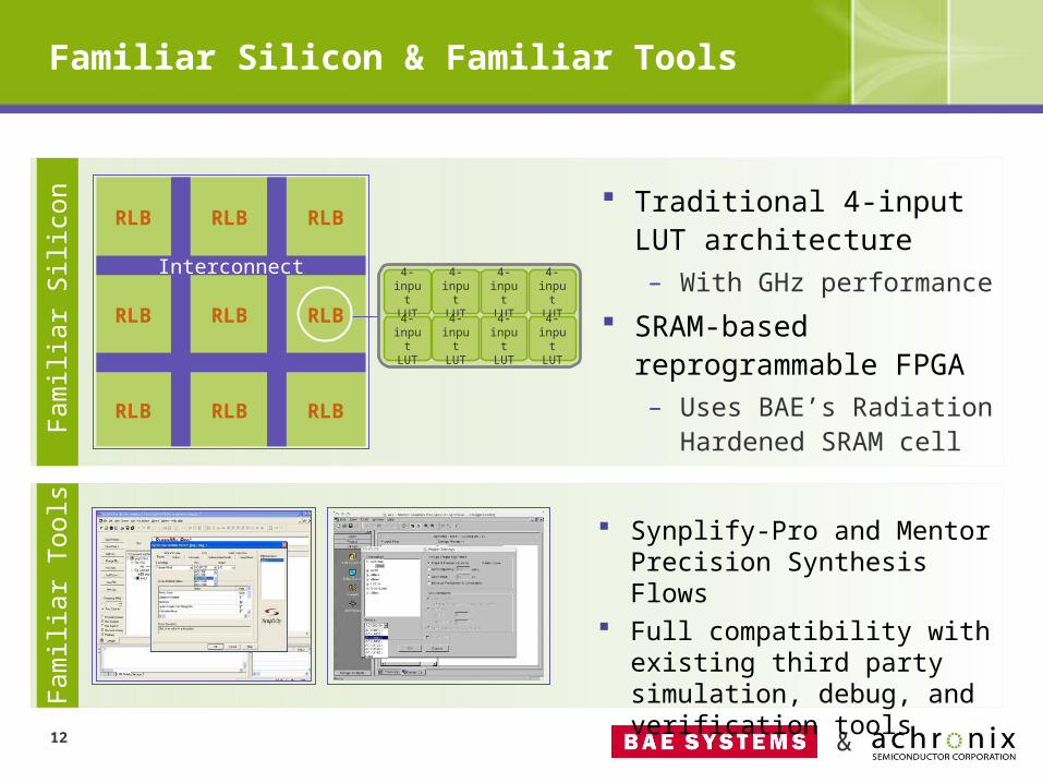
Interconnect
RLB RLB RLB
RLB RLB RLB
RLB RLB RLB
Fam
iliar
Sili
con
4-inputLUT
4-inputLUT
4-inputLUT
4-inputLUT
4-inputLUT
4-inputLUT
4-inputLUT
4-inputLUT
Familiar Silicon & Familiar Tools
Traditional 4-input LUT architecture– With GHz performance
SRAM-based reprogrammable FPGA– Uses BAE’s Radiation
Hardened SRAM cell
Synplify-Pro and Mentor Precision Synthesis Flows
Full compatibility with existing third party simulation, debug, and verification toolsF
amili
ar T
ools

&13
Copy 1
Copy 2
Loca
l Vot
ing
Distance avoids both being affected
by same event
Achronix Patented SEE Mitigation Methodology: Redundancy Voting Circuits (RVC)
Local voting waits until both copies agree– no SEE, values will agree at the voter,
tokens propagate
– When SEE occurs values won’t agree at voter, local voter blocks token propagation
– After event energy dissipates the upset
circuit value is resolved to the correct value and tokens propagate
Redundancy Voting Circuits (RVC)– Two copies of all circuits are implemented
– Copies are non-adjacent to avoid the risk of a single upset affecting both
– Every stage (combinatorial and state) has local voting mechanism

&14
RadRunner Process & Packaging Technology

&15
RadRunner Technology
RadRunner Key Technology Features:Process RH15FThin Oxide / DGO Devices 26 Å / 70 ÅVdd Options 1.5 V / 3.3 VMetal Levels 7Capacitors YesResistors YesMask Levels 33 P1, M1 - OPC CA, CT – Phase ShiftPackage Interface
Product Die Size
Package Type
C4
21.4mm x 21.4mm
624 CCGA

&16
16M SRAM – Next-Generation Strategic RH SRAM
RH15 Process Maturity - Memory
Transistors 113,070,511HVT NFETS 74,422,289HVT PFETS 38,645,756DGO NFETS 1,630DGO PFETS 836R2 Resistors 36,410,528
Q2 Capacitors 18,205,264
Total ILCs 1,063,783,005CA 298,967,451CT 226,146,395V1 212,067,749V2 242,233,858V3 82,209,612V4 1,011,258V5 506,746V6 639,936
Configuration Memory Cell for RadRunner uses the 16M SRAM Cell
Access Time 15-20 ns
Process Technology 0.15 µm CMOS
Die Size 16 mm by 16 mm
Power Supply 1.5 V + / - 10% core2.5 or 3.3 V + / - 10% I/O
Power Dissipation 10 mW/MHz at 1.5V (per die)100 mW standby
Temperature Range -55°C to +125°C
Packaging 23.2 mm by 26.2 mm by 6.0 mm100 pin Flat Pack (5-high stack)
Radiation Hardness Total Ionizing Dose > 1Mrad(Si)Prompt Dose > 1E9 rad(Si)/secSEU < 1E-12 errors / bit-day (W.C. 90% GEO)Latch-up: Immune
ESD Class 2
Screening level Prototype and Flight flows
Organization 2Mx8 die – single chip package2Mx32 4-high package2Mx40 5-high package512Kx32 die – single chip package

&17
RadRunner Package
CGA Package– 624 Total I/O
– Substrate– ceramic 32.5 mm x 32.5 mm
– 25 x 25 Column Grid Array
– 1.27 mm Pitch
– 624 Total I/O
• 223 Signal
192 General Purpose (96 LVDS pairs)
31 Single Ended dedicated I/O
• 4 VCIO / 4 VCREF / 4 VREF
• 182 VDD15 / 18 VDDIO / 4 AVDD
• 184 GND / 1 SR (Seal Ring)
16 Low Inductance Flip Chip Capacitors
Hermetic Seam Weld Sealing– Provides Thermal Enhancement Option

&18
RadRunner Product Features

&19
Die Size: 21.4mm x 21.4mm
Asynchronous Blocks
• Reconfig. Logic Blocks (RLB)
• Routing Resources
• BRAM
Synchronous Blocks
• General Purpose I/O Banks
• Clock and Reset I/O Banks
• PLL
• FPGA Configuration Unit (FCU)
RadRunner Functional Blocks
PLL
General Purpose I /Os
Boundary Elements (BEs)
Bou
ndary
Ele
men
ts (
BEs)
Bou
ndary
Ele
men
ts (
BEs)
Boundary Elements (BEs)
General Purpose I /Os
CLK I/O
CLKI /O
CLK I/O
Genera
l Purp
ose
I/O
s
Genera
l Purp
ose
I/O
s
CLKI /O
CFG
RLB
s
RLB
s
RLB
s
Blo
ck R
AM
RLB
s
RLB
s
RLB
s
RLB
s
RLB
s
RLB
s
RLB
s
RLB
s
RLB
s
RLB
s
RLB
s
RLB
s
RLB
s
ds002_06_v01
PLLsPLLPLLs
Synchronous Asynchronous Blocks (SAB)
• Synchronous to Asynchronous Converter (SAC)
• Asynchronous to Synchronous Converter (ASC)

&20
RadRunner Functional Highlights
Logic Capacity
– 8,640 4-input Look-Up Tables (LUT)
– Ten 200 MHz 18 Kb Two Port (RW) RAM Blocks
Proven Radiation Hardened PLLs (4)
– Reference Frequency range: 22 to 500 MHz
– Output Frequency Range: 25 to 350 MHz
– Lock Time: 200 µs
I/O Capacity and Features
– 192 User Programmable I/Os
– Programmable keeper circuit – Programmable Drive Strengths
– Schmitt Trigger Receivers
– Supported I/O Standards
• LVTTL 3.3 V
• LVCMOS 1.8 V / 2.5 V / 3.3 V
• LVDS 2.5 V with On-Die-Termination
• PCI 3.3V
• SSTL 1.8 V / 2.5 V
• HSTL 1.8 V
– Dedicated SpaceWire I/O Data and Strobe (DS) Clock Recovery Circuits to support link transfer rates up to 125 Mbps

&21
04/21/23
Proposed Achronix RadRunner Product Feature Set
Dev
ice
R
esou
rces
Pac
kage
RadRunner Family (150 nm)

&22
RadRunner BRAM
Each RadRunner device features 10 instances of 18,432 bit Block RAM (BRAM) deployed in a vertical column
The RadRunner Block RAM is implemented with a synchronous BAE memory block wrapped within Achronix asynchronous interface circuits
The block RAM supports two ports, one for writing and one for reading (1W, 1R)
Initialization– Initial content of the block RAMs will be
loaded during device configuration
– Read Port output will be initialized to all zeros
– Data output from last read is retained when read port enable is not asserted
Feature Value
Block RAM Size 18 Kb
Organization 16K x 1, 8K x 2, 4K x 4, 2048 x 9, 2048 x 8, 1024 x 18, 1024 x 16, 512 x 36, 512 x 32
Performance 200 MHz
Physical Implementation
Single column in device
Number of Ports Two ports (1 read and 1 write)
Port Access Synchronous
Contention
Mitigation
Simultaneous Read and Write access from the same address location is not supported

&23
RadRunner SpaceWire Support
The SpaceWire standard1 provides a point-to-point full-duplex serial data communications link
The simple circuitry requirements, low power consumption, and high-link speeds have led to an increased usage of the SpaceWire links and networks
The embedded SpaceWire clock and data recovery circuits support data rates from 2 to 125 Mbps
Each of the 4 I/O banks have dedicated LVDS I/O pairs with hard-wired connections to the received clock-and-data-recovery protocol for the SpaceWire Strobe and Data signals
When not used as SpaceWire I/O pins, these I/O are available as normal general-purpose I/Os
The on-die LVDS termination allows a RadRunner FPGA to interface directly with other SpaceWire capable devices
Link Start Pattern
D
S
Q
QSET
CLR
D
Q
QSET
CLR
D D1
D0
XOR Recovered Clock
Receiver Embedded Logic
FPGA picoPIPE Logic Fabric
Device LVDS Inputs
D
S
XOR Recovered Clock
0 1 1 1 0 1 0 0 1 0 00
SpaceWire Clock & Data Recovery Embedded Circuit
1 European Space Agency Standard: ECSS-E-50-12A
SPACEWIRE
LOCAL
SP
AC
EW
IRE
SP
AC
EW
IRE
SPACEWIRE
LOCALDEVICE
SPACEWIRE
LOCAL
SP
AC
EW
IRE
SP
AC
EW
IRE
SPACEWIRE
LOCALDEVICE
SPACEWIRE
LOCAL
SP
AC
EW
IRE
SP
AC
EW
IRE
SPACEWIRE
LOCALDEVICE
SPACEWIRE
LOCAL
SP
AC
EW
IRE
SP
AC
EW
IRE
SPACEWIRE
LOCALDEVICE
SPACEWIRE LINK
SPACEWIRE LINK
SPACEWIRELINK
SPACEWIRE LINK
SPACEWIRE LINK
SPACEWIRE LINKSPACEWIRE LINK NETWORKMANAGERS
PA
CE
WIR
E
SP
AC
EW
IRE

&24
Overview of Device Configuration Methodology
RadRunner devices may be configured via one of three available options:– IEEE 1149.1 JTAG (via Bitporter)– SPI Flash (on-board Flash
Programming via Bitporter)
– CPU 8 Bit Parallel Interface The Bitporter hardware connects to the
host computer (Linux or Windows) through one of two available options:– Universal Serial Bus (USB) – 10/100 Ethernet port
The Bitporter connects directly to the chip via an EJTAG compliant connector
Bitporter control software can be run from either the Windows or Linux operating systems– Available as a stand-alone utility
or integrated into the ACE environment
EJTAG compliant connector
2.54 mm
1413
2.54 mm
21
Top View PCB
0.64 mm
5.84 mm
Side View PCB
1
Signal Positions
GNDTRST*
GNDTDI
GNDTDO
GNDTMS
GNDTCK
keyNC
VIONC
Pin 12 removed to allow for key

&25
Friday, April 21, 2023
Block Diagram of Configuration Checker
Configuration Data Checker Description– A Finite State Machine (FSM) within the FPGA
Configuration Unit (FCU) manages the process of checking the validity of the configuration bits • CFG_CHK_ENABLE is a dedicated external static input
signal to enable or disable the checking process when the FCU state machine enters user mode
• A Programmable delay counter allows user to specify delay between configuration check cycles
– When enabled the configuration-data checker runs in the following sequence:• A 32-bit Cyclic Redundancy Code (CRC32) is calculated
for the configuration data of the RadRunner Core configuration bits (except the BRAM)
The ACE tools compute a CRC32 signature which gets loaded into the part during the configuration process
When this CRC32 signature gets included in the calculation the resulting CRC32 quotient should result in a fixed value ─ 32’h0704DD7B
• An XOR chain computes the parity of the S-Frame configuration bits
S-Frame configuration bits get stored in a manner similar to a serial shift register
The final parity result of the S-frame calculation is compared to a pre-determined (by ACE) value
• CFG_MEM_ERR, an external device output will be asserted when either the CRC32 or XOR parity computation are incorrect
S-F
ram
e
Achronix Radrunner FPGA
FCU
picoPIPE Logic Fabric
FPGA Core Configuration (minus BRAM) CRC-32
check
S-Frame configuration bits (serial shift registers)
Q
QSET
CLR
D
Q
QSET
CLR
D
Q
QSET
CLR
D
Q QS
ET
CLR
D
Q QS
ET
CLR
D
Q QS
ET
CLR
D
Q QS
ET
CLR
D
Q QS
ET
CLR
D
Q QS
ET
CLR
D
Q
Q SET
CLR
D
Q
Q SET
CLR
D
Q
Q SET
CLR
D
Q
QSET
CLR
D
Q
QSET
CLR
D
Q
QSET
CLR
D
QQS
ET
CLR
D
QQS
ET
CLR
D
QQS
ET
CLR
D
QQS
ET
CLR
D
QQS
ET
CLR
D
QQS
ET
CLR
D
FCU
Delay Set
FSM
CRC CheckParity bit Check
Config check error

&26
SUMMARY
Program Fulfills Critical Need for Reconfigurable RH FPGAs for Strategic Applications
Excellent Partnership between BAE Systems and Achronix Ongoing
Initial Achronix Commercial Chip First Pass Success
Test Chip Functionality Demonstrated, Radiation Testing Successful
RadRunner Completing Fabrication
Proof-Of-Concept Demonstration to be completed 4Q09