Embed Size (px)
Citation preview

Reconfigurable Antenna Aperture with Optically Controlled GeTe-Based RF Switches
Loc Chau1, James G. Ho1, Xing Lan1, Norma Riley1, Robert M. Young2, Nabil El-Hinnawy2, Doyle Nichols2, John Volakis3, Nima Ghalichechian3
1Northrop Grumman Aerospace Systems, Redondo Beach, CA 90278
2Northrop Grumman Electronic Systems, Linthicum, MD 21090
3The Ohio State University, Columbus, OH 43212
Abstract: We have characterized the ON state DC
electrical resistivity and OFF state capacitance of GeTe-
Based RF Switches under direct optical laser excitation.
Our tightly-coupled dipole array exhibits performance in
excess of 4 to 1 bandwidth over wide-scan angle up to 60
degrees with in-band rejection capability using
reconfigurable baluns. Integration of optically-controlled
GeTe-Based RF switches at the antenna aperture extends
reconfiguration flexibility.
Keywords: Phase change material; GeTe; RF switches;
direct optical laser excitation; tightly-coupled dipole array;
wide-scan; wideband; reconfigurable balun.
Introduction Modern military phased array antenna systems for radar
and communication applications in a contested
environment require being flexible, adaptable and
reconfigurable. There is a growing demand for
reconfigurable antenna systems with increased mission
functionality and decreased developmental timescales at
reduced fielded system cost. In addition, there is a strong
desire to aggregate both narrow and wideband antennas on
platforms to reduce interference, maintenance, and air-
worthiness certifications.
Well-known connecting array architectures [1]-[5],
including connecting bowtie, tightly-coupled dipole, planar
ultra wideband modular antenna, and thumbtack arrays,
have been demonstrated to exhibit very wide bandwidth
over large scan angle. This design approach departs from
these conventional phased array antenna systems by
synthesizing reconfigurable baluns and optically-controlled
phase change material bridges to form an innovative
antenna aperture that allows in-field and on-the-fly
adjustments to linearity, bandwidth, polarization , and
frequency to fit many mission scenarios and system needs.
Theory of Operation In the proposed reconfigurable connected array (Fig. 1),
switch bridges in the printed radiator surface, implemented
using phase change material (PCM), enable individual
radiating elements to be interconnected in a wide variety of
shapes to control the spatial pattern. The toggling control of
the PCM bridges is achieved using a pulsed laser to heat
individual GeTe PCM switch elements. The laser energy is
delivered via optical fibers. At the array level, multiple
PCM switch elements share a common laser source
connected to an optical fiber switch. The radiating element
is fed by a novel wideband balun capable of providing fine
frequency and bandwidth tuning over wide instantaneous
bandwidth. The reconfigurable balun is a Marchand type,
Figure 1. Block diagram of integrated optically-controlled pixelated connected array
Pixelated Planar Connected Array Single Mode Fibers
Micro Beam Shaping Optics Deliver Activation Energy to
PCM Bridges
Circuit Diagram of Four Switch Phase Change
Material Bridge
Fiber Switch
Laser Driver for PCM Bridge
Activation
Tunable Marchand Balun
with MEMS Switches and
Tunable Capacitors
Source
Single Mode Fibers
Aperture Feeds
349
which includes the interplay of the open and shorted stubs.
Strategic insertion of switches, tunable LC loading, or
capacitive loading within the balun structure allow
flexibility in reconfiguration of center operating frequency,
band selection and band rejection.
Enable Components Referring to Fig. 1, the integrated reconfigurable aperture
includes PCM bridges, reconfigurable balun, and optical
control circuit. The following subsections provide details
on each component’s design and implementation.
PCM Switch: The RF switch material is based on phase
change phenomena exhibited by the chalcogenide family of
materials. The material development had been previously
demonstrated [6]-[8]. The first demonstration of in line
phase change RF switch with integrated thin film heater
had been reported by El-Hinnawy et al. [9]. In this report,
the heat source is generated by a laser pulse. Depending on
the magnitude of temperature rise and the cooling rate,
crystalline or amorphous phases will be formed. To change
states, Fig. 2, a heat pulse with short duration (~100ns) but
high amplitude raises the material’s temperature above the
melting point. As a liquid, the atoms are randomly
distributed relative to their neighbors. Rapid quench
cooling (~100ns) then freezes these atoms into an
amorphous solid, locking in a high electrical resistance
state. By contrast, application of a longer pulse width with
moderate amplitude raises the material’s temperature
slightly above the crystallization temperature. If the pulse is
of appropriately long duration, the structure experiences
atomic bond rearrangement and leads to the low resistance
phase. The material offers an off/on ratio of 2x10⁷ when
comparing the as deposited amorphous state and the
crystalline state.
Figure 2. Temperature-dependent PCM State Change
Low On-state resistivity is achievable using PCM bridge
geometries with high aspect ratio. Fig. 3 shows the thermal
model developed to determine the optimum PCM bridge
configuration for a given laser excitation. It is shown that
for a 1W laser source pulsed at 100ns, there is sufficient
optical energy to heat and melt a 100nm thick GeTe PCM
area of approximately 3µm2.
Figure 3. Optimum PCM area under direct laser excitation
The thermal model provides accurate prediction of
minimum power to amorphize under laser excitation, as
shown in Fig. 4, which tracks well with previously
published thin film heater model [9].
Figure 4. Validation of Melt/Quench Thermal Model
Optical Control: The optical fiber coupled laser light,
which will be used to activate PCM switch transition, offers
a light weight, scalable, highly localized energy delivery to
350
each switching element with near zero disturbances to the
antenna radiation pattern. Precision power and timing
profiles of optical pulses controlled by pulser electronics
are shown in Fig. 5. A laser pulse of approximately 2.5W
with 100ns pulse width is required to change the GeTe
PCM switch from the crystallized state to an amorphous
state. Smaller laser power amplitude of approximately 1W
with longer pulse duration of 1.5µs is needed for
recrystallization. Fig. 6 shows an image of the test setup for
direct laser excitation of GeTe PCM switches.
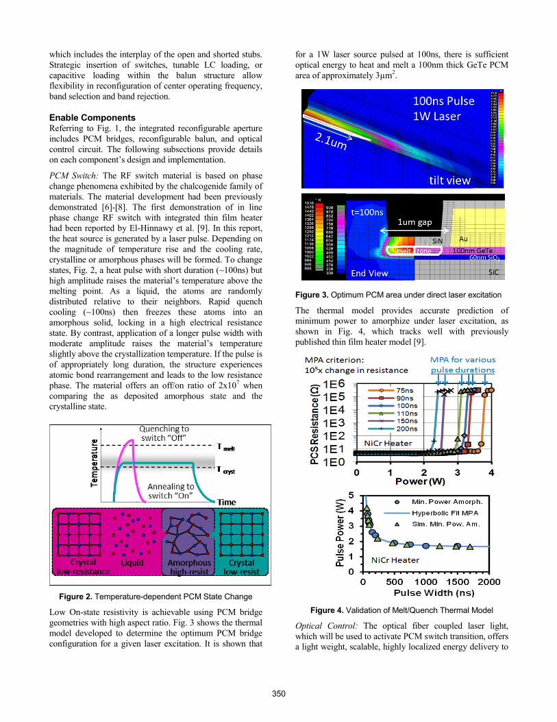
Figure 6. Optical bench test of GeTe PCM switch
The DC resistivity measurement is made using a Keithley
Pico-Amp Meter with a 3-tip probe at 200µm pitch, shown
on the right hand side of the image. False color image of
GeTe PCM bridge 15x5µm (LxW) at the switched sates is
shown in Fig. 7. Prior to laser excitation, the PCM bridge is
measured at 103Ω (left image). The PCM bridge off state is
measured at 4.4 KΩ after laser activation (right image).
These values are consistent with electrically activated PCM
bridge devices.
Figure 7. True/False Color Image of PCM at ON & OFF
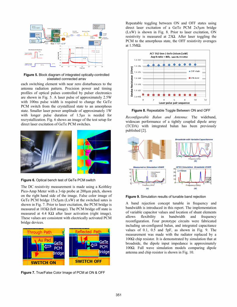
Repeatable toggling between ON and OFF states using
direct laser excitation of a GeTe PCM 2x5µm bridge
(LxW) is shown in Fig. 8. Prior to laser excitation, ON
resistivity is measured at 23Ω. After laser toggling the
PCM to the amorphous state, the OFF resistivity averages
at 1.5MΩ.
Figure 8. Repeatable Toggle Between ON and OFF
Reconfigurable Balun and Antenna: The wideband,
widescan performance of a tightly coupled dipole array
(TCDA) with integrated balun has been previously
published [2].
Figure 9. Simulation results of tunable band rejection
A band rejection concept tunable in frequency and
bandwidth is introduced in this report. The implementation
of variable capacitor values and location of shunt elements
allows flexibility in bandwidth and frequency
reconfiguration. Four prototype circuits were fabricated
including un-configured balun, and integrated capacitance
values of 0.1, 0.5 and 5pF, as shown in Fig. 9. The
measurement was made with the radiator replaced by a
100Ω chip resistor. It is demonstrated by simulation that at
broadside, the dipole input impedance is approximately
100Ω. Full wave simulation models comparing dipole
antenna and chip resistor is shown in Fig. 10.
Figure 5. Block diagram of integrated optically-controlled
pixelated connected array
351
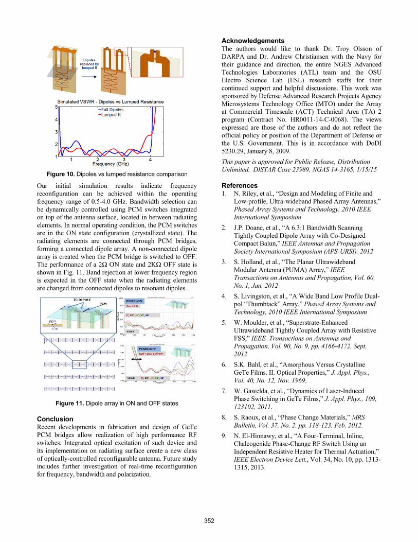
Figure 10. Dipoles vs lumped resistance comparison
Our initial simulation results indicate frequency
reconfiguration can be achieved within the operating
frequency range of 0.5-4.0 GHz. Bandwidth selection can
be dynamically controlled using PCM switches integrated
on top of the antenna surface, located in between radiating
elements. In normal operating condition, the PCM switches
are in the ON state configuration (crystallized state). The
radiating elements are connected through PCM bridges,
forming a connected dipole array. A non-connected dipole
array is created when the PCM bridge is switched to OFF.
The performance of a 2Ω ON state and 2KΩ OFF state is
shown in Fig. 11. Band rejection at lower frequency region
is expected in the OFF state when the radiating elements
are changed from connected dipoles to resonant dipoles.
Figure 11. Dipole array in ON and OFF states
Conclusion Recent developments in fabrication and design of GeTe
PCM bridges allow realization of high performance RF
switches. Integrated optical excitation of such device and
its implementation on radiating surface create a new class
of optically-controlled reconfigurable antenna. Future study
includes further investigation of real-time reconfiguration
for frequency, bandwidth and polarization.
Acknowledgements
The authors would like to thank Dr. Troy Olsson of
DARPA and Dr. Andrew Christiansen with the Navy for
their guidance and direction, the entire NGES Advanced
Technologies Laboratories (ATL) team and the OSU
Electro Science Lab (ESL) research staffs for their
continued support and helpful discussions. This work was
sponsored by Defense Advanced Research Projects Agency
Microsystems Technology Office (MTO) under the Array
at Commercial Timescale (ACT) Technical Area (TA) 2
program (Contract No. HR0011-14-C-0068). The views
expressed are those of the authors and do not reflect the
official policy or position of the Department of Defense or
the U.S. Government. This is in accordance with DoDI
5230.29, January 8, 2009.
This paper is approved for Public Release, Distribution
Unlimited. DISTAR Case 23989, NGAS 14-3165, 1/15/15
References 1. N. Riley, et al., “Design and Modeling of Finite and
Low-profile, Ultra-wideband Phased Array Antennas,”
Phased Array Systems and Technology, 2010 IEEE
International Symposium
2. J.P. Doane, et al., “A 6.3:1 Bandwidth Scanning
Tightly Coupled Dipole Array with Co-Designed
Compact Balun,” IEEE Antennas and Propagation
Society International Symposium (APS-URSI), 2012
3. S. Holland, et al., “The Planar Ultrawideband
Modular Antenna (PUMA) Array,” IEEE
Transactions on Antennas and Propagation, Vol. 60,
No. 1, Jan. 2012
4. S. Livingston, et al., “A Wide Band Low Profile Dual-
pol “Thumbtack” Array,” Phased Array Systems and
Technology, 2010 IEEE International Symposium
5. W. Moulder, et al., “Superstrate-Enhanced
Ultrawideband Tightly Coupled Array with Resistive
FSS,” IEEE Transactions on Antennas and
Propagation, Vol. 90, No. 9, pp. 4166-4172, Sept.
2012
6. S.K. Bahl, et al., “Amorphous Versus Crystalline
GeTe Films. II. Optical Properties,” J. Appl. Phys.,
Vol. 40, No. 12, Nov. 1969.
7. W. Gawelda, et al., “Dynamics of Laser-Induced
Phase Switching in GeTe Films,” J. Appl. Phys., 109,
123102, 2011.
8. S. Raoux, et al., “Phase Change Materials,” MRS
Bulletin, Vol. 37, No. 2, pp. 118-123, Feb. 2012.
9. N. El-Hinnawy, et al., “A Four-Terminal, Inline,
Chalcogenide Phase-Change RF Switch Using an
Independent Resistive Heater for Thermal Actuation,”
IEEE Electron Device Lett., Vol. 34, No. 10, pp. 1313-
1315, 2013.
352