Embed Size (px)
Citation preview

www.advmat.dewww.MaterialsViews.com
REV
IEW
Recent Trends in Surface Characterization and Chemistry with High-Resolution Scanning Force Methods
Clemens Barth , * Adam S. Foster , * Claude R. Henry , and Alexander L. Shluger *The current status and future prospects of non-contact atomic force micro-scopy (nc-AFM) and Kelvin probe force microscopy (KPFM) for studying insulating surfaces and thin insulating fi lms in high resolution are discussed. The rapid development of these techniques and their use in combination with other scanning probe microscopy methods over the last few years has made them increasingly relevant for studying, controlling, and functional-izing the surfaces of many key materials. After introducing the instruments and the basic terminology associated with them, state-of-the-art experimental and theoretical studies of insulating surfaces and thin fi lms are discussed, with specifi c focus on defects, atomic and molecular adsorbates, doping, and metallic nanoclusters. The latest achievements in atomic site-specifi c force spectroscopy and the identifi cation of defects by crystal doping, work function, and surface charge imaging are reviewed and recent progress being made in high-resolution imaging in air and liquids is detailed. Finally, some of the key challenges for the future development of the considered fi elds are identifi ed.
1. Introduction The family of scanning probe microscopy (SPM) methods employing forces for studying surface properties has devel-oped over the last 25 years into many versatile tools in surface
© 2011 WILEY-VCH Verlag GmbH & Co. KGaA, WeinheiAdv. Mater. 2011, 23, 477–501
Dr. C. Barth , Dr. C. R. Henry Centre Interdisciplinaire de Nanoscience de Marseille (CINaM, The CINaM is associated with the Aix-Marseille University)CNRS, Campus de LuminyCase 913, 13288 Marseille Cedex 09, France E-mail: [email protected] Prof. A. S. Foster Department of PhysicsTampere University of TechnologyP.O. Box 692, FIN-33101 Tampere, Finland E-mail: [email protected] Prof. A. S. Foster Department of Applied PhysicsAalto University School of Science and TechnologyPO Box 11100 FI-00076 Helsinki, Finland Prof. A. L. Shluger Department of Physics and Astronomy and the London Centre for NanotechnologyUniversity College LondonGower Street, London, WC1E 6BT, UK E-mail: [email protected] Prof. A. L. Shluger WPI-Advanced Institute of Materials ResearchTohoku University2-1-1 Kitahira, Aoba, Sendai, 980-8577, Japan
DOI: 10.1002/adma.201002270
physics and chemistry, as well as in nano-science and nanotechnology. Phenomena studied by these techniques include sur-face topography; atomic structure; fi lm growth; measurements of adhesion and the strength of individual chemical bonds; friction and lubrication; work functions; electrostatic, dielectric and magnetic properties; contact charging; molecular manipulation; and many others from the micrometer to the subnanometer scale. Different members of the force micros-copy family specialize in different surface properties and operate in different envi-ronments and temperatures ranging from low temperatures and ultra high vacuum (UHV), to room temperatures and above, in air and in liquids. In this paper, we focus on the recent applications of two of the most commonly used techniques, non-contact atomic force microscopy (nc-
AFM) and Kelvin probe force microscopy (KPFM), to studying surfaces of insulators and thin fi lms with atomic or nanoscale resolution. A major strength of these techniques is their lack of material restrictions, and many of the breakthrough results in high-resolution imaging have been achieved on surfaces inaccessible to other imaging techniques. The requirement of a conducting sample has long prevented studies of insulators with scanning tunneling microscopy (STM) in particular and the focus of this review on insulators has been directed by the success of force microscopy in this area. Furthermore, these materials have proven to be critical in many recent applications, such as catalysis, sensors, microelectronics, and molecular electronics.
In both nc-AFM and KPFM a sharp tip interacts with the sur-face and a surface image is produced by scanning. However, the forces dominating the image formation are different. In atomic force microscopy (AFM) the control parameter is the total force between the tip and sample, including the short-range interac-tion providing the nanoscale and atomic image contrast. KPFM is actually a suite of techniques implemented into nc-AFM, offering the measurement of local work function changes on conducting surfaces and the surface charge distribution on insulating sur-faces. KPFM is dominated by long-range electrostatic forces, with short-range forces contributing to atomic contrast. In both tech-niques, information about the system under study is encoded in a change of these forces as the tip scans along the surface. These techniques belong to the much bigger family of SPM methods, a number of which are briefl y described in Table 1 for reference. Providing a detailed description of each of these techniques is
477m wileyonlinelibrary.com 477
www.advmat.dewww.MaterialsViews.com
REV
IEW
478
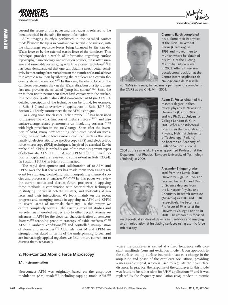
Clemens Barth completed his diplomarbeit in physics at the Freie Universität Berlin (Germany) in 1999 and moved then to Munich where he obtained his Ph.D. at the Ludwig-Maximilians-Universität in 2002. After a three year postdoctoral position at the Centre Interdisciplinaire de Nanoscience de Marseille
(CINaM) in France, he became a permanent researcher in the CNRS at the CINaM in 2004.
Adam S. Foster obtained his masters degree in theo-retical physics at Newcastle University (UK) in 1997 and his Ph.D. at University College London (UK) in 2000. After a postdoctoral position in the Laboratory of Physics, Helsinki University of Technology (Finland), he became an Academy of Finland Senior Fellow in
2004 at the same lab. He was appointed Professor at the Department of Physics, Tampere University of Technology (Finland) in 2009.
Alexander Shluger gradu-ated from the Latvia State University, Riga, in 1976 and received his Ph.D. and Doctor of Science degrees from the L. Karpov Physics and Chemistry Research Institute (Moscow) in 1981 and 1988, respectively. He became a Professor of Physics at the University College London in 2004. His research is focused
on theoretical studies of defects in insulators and imaging and manipulation at insulating surfaces using atomic force microscopy.
beyond the scope of this paper and the reader is referred to the literature cited in the table for more information.
AFM imaging is often performed in the so-called contact mode, [ 1 ] where the tip is in constant contact with the surface, with the short-range repulsive forces being balanced by the van der Waals force or by the external elastic force of the cantilever. This technique provides a wealth of information regarding surface topography, nanotribology, and adhesion physics, but is often inva-sive and unreliable for imaging with true atomic resolution. [ 2 , 3 ] It has been demonstrated that one can obtain a much better sensi-tivity in measuring force variations on the atomic scale and achieve true atomic resolution by vibrating the cantilever at a certain fre-quency above the surface. [ 4 , 27 ] In this case, the elastic force on the cantilever overcomes the van der Waals attraction of a tip to a sur-face and prevents the so called “jump-into-contact”. [ 2,5 ] Since the tip is then not in permanent direct hard contact with the surface, this technique is often also called non-contact AFM (nc-AFM). A detailed description of the technique can be found, for example, in Refs. [ 5–7 ] and an overview of applications in Refs. [ 1 , 5 , 7–10 ] . Section 2.1 briefl y summarizes the nc-AFM technique.
For a long time, the classical Kelvin probe [ 11 , 12 ] has been used to measure the work function of metal surfaces [ 13–15 ] and also surface-charge-related phenomena on insulating surfaces [ 16–20 ] with high precision in the meV range. Soon after the inven-tion of AFM, many new scanning techniques based on meas-uring the electrostatic forces were introduced, such as the large family of electrostatic force spectroscopy (EFS) and electrostatic force microscopy (EFM) techniques. Inspired by classical Kelvin probe, [ 21 , 22 ] KPFM is probably one of the most important types of electrostatic AFM. EFS, EFM, and KPFM differ in their func-tion principle and are reviewed to some extent in Refs. [ 23 , 24 ]. In Section 3 KPFM is briefl y summarized.
The rapid development and collaboration of nc-AFM and KPFM over the last few years has made them increasingly rel-evant for studying, controlling, and manipulating chemical spe-cies and processes at surfaces. [ 8,10,25,26 ] In this paper we review the current status and discuss future prospects in applying these methods in combination with other surface techniques to studying individual defects, clusters, and molecules at sur-faces and their interactions. We focus mainly on the recent progress and emerging trends in applying nc-AFM and KPFM in several areas of materials chemistry. In this review we cannot completely cover all the existing excellent studies and we refer an interested reader also to other recent reviews on advances in AFM for the electrical characterization of semicon-ductors, [ 28 ] scanning probe microscopy of oxide surfaces, [ 29–31 ] AFM in ambient conditions, [ 32 ] and controlled manipulation of atoms and molecules. [ 33 ] Although nc-AFM and KPFM are strongly interrelated in terms of the underpinning forces, and are increasingly applied together, we fi nd it more convenient to discuss them separately.
2. Non-Contact Atomic Force Microscopy
2.1. Instrumentation
Non-contact AFM was originally based on the amplitude modulation (AM) mode, [ 34 ] including tapping mode AFM, [ 35 ]
© 2011 WILEY-VCH Verlag Gmwileyonlinelibrary.com
where the cantilever is excited at a fi xed frequency with con-stant amplitude (constant excitation mode). Upon approach to the surface, the tip–surface interaction causes a change in the amplitude and phase of the cantilever oscillations, providing a measurable signal, which is used to regulate the tip–surface distance. In practice, the response of the cantilever in this mode was found to be rather slow for UHV applications, [ 6 ] and it was replaced by the frequency modulation (FM) mode [ 6 ] in atomic
bH & Co. KGaA, Weinheim Adv. Mater. 2011, 23, 477–501

www.advmat.dewww.MaterialsViews.com
REV
IEW
479© 2011 WILEY-VCH Verlag GmbH & Co. KGaA, WeinheimAdv. Mater. 2011, 23, 477–501 wileyonlinelibrary.com 479
Table 1. Key features of different high-resolution SPM techniques. Terms such as electrostatic modulation/contribution and 1st and 2nd harmonic are explained in Section 3. More details about each technique can be found in the selected references. Note that the references are only a part of the whole literature. For a complete understanding of the techniques, the reader should also study the literature, which is cited or cites the references in the table.
Base Technique Mode Dynamic Characteristics/Notes Feedback for tip–surface distance
Measured signals, images
Typical tip–surface distance
(nm)
Literature
Scanning Tun-
neling Microscopy
STM No Tunneling current Topography 0.6–1.0 [9, 326,
327]
Atomic Force
Microscopy
Contact (c-AFM) No Cantilever defl ection
(normal force, F N )
Topography, lateral
force
short-range,
repulsive tip–
surface
interaction
[1, 2, 369]
Amplitude mod-
ulated nc-AFM
(AM nc-AFM)
Yes Constant excitation at
constant frequency
Amplitude, A , or
phase, φ
Topography,
dissipation
1.0–5.0 [6, 7]
Frequency modu-
lated nc-AFM
(FM nc-AFM)
Yes 2 nd loop for constant
amplitude regulationFrequency change, Δ f Topography,
dissipation
0.3–5.0 [5, 6, 7]
Tapping mode
AFM
Yes In principle, AM nc-AFM
with very large amplitudes,
tip–surface contact
Amplitude, A , or
phase, φ
Topography,
dissipation
Short-range,
repulsive tip–sur-
face interaction
[35]
Constant height
mode AFM
Yes/No Can be applied either in
c-AFM or AM/FM nc-AFM
None or very slow feed-
back on F N (c-AFM),
Δ f (FM nc-AFM), or A
(AM nc-AFM)
F N (c-AFM), Δ f (FM
nc-AFM), or A (AM
nc-AFM) + dissipation
in nc-AFM
0.3–5.0 [36, 37, 38]
Electrostatic Force
Spectroscopy
(EFS)
Spectroscopy Yes Dependence on voltage or
time or distance; Electro-
static modulation can be
applied
No feedback, the tip
is fi xed above the
surface
nc-AFM signals ( Δ f or
A , dissipation) or 1 st
harmonic of the elec-
trostatic contribution
0.5–5.0 [370, 305,
314, 380]
Electrostatic Force
Microscopy (EFM)
Normal topog-
raphy imaging in
nc-AFM; Single-
pass method
Yes The image evolution is
observed either in depen-
dence on time or voltage,
from image to image
nc-AFM feedback Piezo elongation in z
(topography signal)
1.0–5.0 [302, 370,
371, 372]
Double-pass
mode
n.a. After a topography image
or scanning line has been
obtained, the tip is placed
at a distance of 10–100 nm
above the surface for elec-
trostatic force detection of
the same surface area
No feedback Either detuning Δ f
or phase, φ , of the
cantilever resonance
frequency or 1 st
harmonic of the elec-
trostatic contribution
10–100 [23, 373]
Single-pass
mode
Yes Normal nc-AFM imaging +
electrostatic modulation
nc-AFM feedback 1 st and 2 nd harmonic
of the electrostatic
contribution
1.0–5.0 [374, 375,
376]
Scanning Polariza-
tion Force Micros-
copy (SPFM)
Single-pass
mode
Yes The 2 nd harmonic of the
electrostatic contribution
is used for the tip–surface
distance regulation (FM and
AM nc-AFM)
2 nd harmonic of
the electrostatic
contribution
1 st harmonic of the
electrostatic contribu-
tion and piezo elonga-
tion in z (topography
signal)
1.0–5.0 [377, 378,
379]
Kelvin Probe
Force Microscopy
(KPFM)
Frequency modu-
lation, single-
pass mode
Yes The frequency of the electro-
static modulation is much
smaller than the cantilever
resonance frequency, typi-
cally < 5 kHz
nc-AFM feedback +
Kelvin loop
Tip–surface contact
potential difference
Normal distance:
1.0–5.0 (atomic
resolution closer)
[294, 296,
297]
Amplitude
modulation,
single-pass
mode
Yes The frequency of the ac
voltage is mostly put onto
the 1 st harmonic of the can-
tilever oscillation (6.3 x canti-
lever resonance frequency)
nc-AFM feedback +
Kelvin loop
Tip–surface contact
potential difference
Normal distance:
1.0–5.0 (atomic
resolution closer)
[295, 296,
297]
www.advmat.dewww.MaterialsViews.com
REV
IEW
480
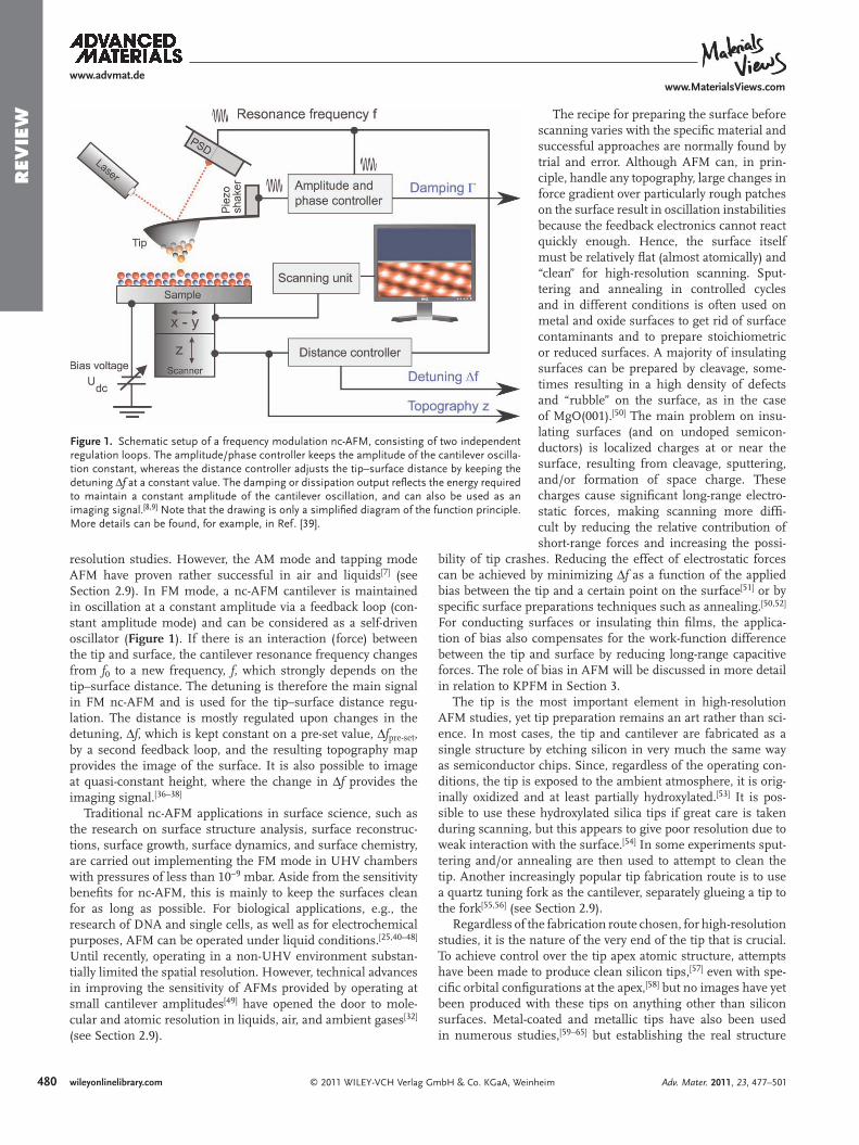
Figure 1 . Schematic setup of a frequency modulation nc-AFM, consisting of two independent regulation loops. The amplitude/phase controller keeps the amplitude of the cantilever oscilla-tion constant, whereas the distance controller adjusts the tip–surface distance by keeping the detuning Δ f at a constant value. The damping or dissipation output refl ects the energy required to maintain a constant amplitude of the cantilever oscillation, and can also be used as an imaging signal. [ 8 , 9 ] Note that the drawing is only a simplifi ed diagram of the function principle. More details can be found, for example, in Ref. [ 39 ] .
resolution studies. However, the AM mode and tapping mode AFM have proven rather successful in air and liquids [ 7 ] (see Section 2.9). In FM mode, a nc-AFM cantilever is maintained in oscillation at a constant amplitude via a feedback loop (con-stant amplitude mode) and can be considered as a self-driven oscillator ( Figure 1 ). If there is an interaction (force) between the tip and surface, the cantilever resonance frequency changes from f 0 to a new frequency, f , which strongly depends on the tip–surface distance. The detuning is therefore the main signal in FM nc-AFM and is used for the tip–surface distance regu-lation. The distance is mostly regulated upon changes in the detuning, Δ f , which is kept constant on a pre-set value, Δ f pre-set , by a second feedback loop, and the resulting topography map provides the image of the surface. It is also possible to image at quasi-constant height, where the change in Δ f provides the imaging signal. [ 36–38 ]
Traditional nc-AFM applications in surface science, such as the research on surface structure analysis, surface reconstruc-tions, surface growth, surface dynamics, and surface chemistry, are carried out implementing the FM mode in UHV chambers with pressures of less than 10 − 9 mbar. Aside from the sensitivity benefi ts for nc-AFM, this is mainly to keep the surfaces clean for as long as possible. For biological applications, e.g., the research of DNA and single cells, as well as for electrochemical purposes, AFM can be operated under liquid conditions. [ 25 , 40–48 ] Until recently, operating in a non-UHV environment substan-tially limited the spatial resolution. However, technical advances in improving the sensitivity of AFMs provided by operating at small cantilever amplitudes [ 49 ] have opened the door to mole-cular and atomic resolution in liquids, air, and ambient gases [ 32 ] (see Section 2.9).
© 2011 WILEY-VCH Verlag GmbH & Co. KGaA, Wewileyonlinelibrary.com
The recipe for preparing the surface before scanning varies with the specifi c material and successful approaches are normally found by trial and error. Although AFM can, in prin-ciple, handle any topography, large changes in force gradient over particularly rough patches on the surface result in oscillation instabilities because the feedback electronics cannot react quickly enough. Hence, the surface itself must be relatively fl at (almost atomically) and “clean” for high-resolution scanning. Sput-tering and annealing in controlled cycles and in different conditions is often used on metal and oxide surfaces to get rid of surface contaminants and to prepare stoichiometric or reduced surfaces. A majority of insulating surfaces can be prepared by cleavage, some-times resulting in a high density of defects and “rubble” on the surface, as in the case of MgO(001). [ 50 ] The main problem on insu-lating surfaces (and on undoped semicon-ductors) is localized charges at or near the surface, resulting from cleavage, sputtering, and/or formation of space charge. These charges cause signifi cant long-range electro-static forces, making scanning more diffi -cult by reducing the relative contribution of short-range forces and increasing the possi-
bility of tip crashes. Reducing the effect of electrostatic forces can be achieved by minimizing Δ f as a function of the applied bias between the tip and a certain point on the surface [ 51 ] or by specifi c surface preparations techniques such as annealing. [ 50 , 52 ] For conducting surfaces or insulating thin fi lms, the applica-tion of bias also compensates for the work-function difference between the tip and surface by reducing long-range capacitive forces. The role of bias in AFM will be discussed in more detail in relation to KPFM in Section 3.
The tip is the most important element in high-resolution AFM studies, yet tip preparation remains an art rather than sci-ence. In most cases, the tip and cantilever are fabricated as a single structure by etching silicon in very much the same way as semiconductor chips. Since, regardless of the operating con-ditions, the tip is exposed to the ambient atmosphere, it is orig-inally oxidized and at least partially hydroxylated. [ 53 ] It is pos-sible to use these hydroxylated silica tips if great care is taken during scanning, but this appears to give poor resolution due to weak interaction with the surface. [ 54 ] In some experiments sput-tering and/or annealing are then used to attempt to clean the tip. Another increasingly popular tip fabrication route is to use a quartz tuning fork as the cantilever, separately glueing a tip to the fork [ 55 , 56 ] (see Section 2.9).
Regardless of the fabrication route chosen, for high-resolution studies, it is the nature of the very end of the tip that is crucial. To achieve control over the tip apex atomic structure, attempts have been made to produce clean silicon tips, [ 57 ] even with spe-cifi c orbital confi gurations at the apex, [ 58 ] but no images have yet been produced with these tips on anything other than silicon surfaces. Metal-coated and metallic tips have also been used in numerous studies, [ 59–65 ] but establishing the real structure
inheim Adv. Mater. 2011, 23, 477–501

www.advmat.dewww.MaterialsViews.com
REV
IEW
of a tip apex remains challenging and evidence of real control over tip structure is still lacking. In some cases the tip was modifi ed by controlled adsorption of molecules [ 66 , 67 ] or even carbon nanotubes, [ 68–70 ] but while these offer improvements in stability for lower-resolution imaging, they have not yet been routinely successful for high-resolution studies. Even if the last atom of the tip can be identifi ed, it has to be guaranteed that the tip does not change during an AFM measurement. Tip changes, however, appear regularly during scanning until the chemical potential equilibrium between tip and sample is (at least temporarily) formed. Therefore the chemical composition of the last atoms of the tip is extremely diffi cult to control. This is why tips are often purposely brought into contact with the surface, in an attempt to facilitate establishing such an equilib-rium, with the hope that a sensitive, but also stable, nanotip is formed.
Recently, metallic tips functionalized by adsorption of Cl atoms and CO molecules have been used successfully to resolve the atomic structure of pentacene and other molecules adsorbed on NaCl fi lms on Cu(111). [ 64 ] This approach provides a potential route to achieve a degree of control over the tip structure, but it has been implemented so far only using a combined STM/AFM instrument at low temperature in a system featuring thin NaCl islands on a metal surface. This allowed picking up atoms and molecules in a controlled fashion from the metal surface using the instrument in the STM mode of operation. The appli-
Figure 2 . a) High resolution nc-AFM image of a mixture of Sn, Pb and Si atoms on the Si (111) surface and b) sets of force curves measured over Pb and Si atoms. The discrimination between the different atomic species could be accomplished by comparing experimental and theoretical force spectroscopy. c) 3D force spectroscopy of the graphite surface. Panels (a,b) reproduced with permission. [73] Copyright 2007, Nature Publishing Group. Panel (c) reproduced with per-mission. [74] Copyright 2009, Nature Publishing Group.
cability of this technique to a wider variety of substrates has yet to be demonstrated.
2.2. Methods and Challenges in Interpretation of nc-AFM Images
The overall strength of the interaction between tips and surfaces is mainly deter-mined by long-range van der Waals and elec-trostatic forces. However, the atomic contrast in nc-AFM images is dominated by short-range van der Waals, electrostatic, and cova-lent interactions between the tip apex and the atoms in the surface. [ 7 , 9 , 71 , 72 ] It is an over-sim-plifi cation to consider this to be equivalent to a single atom at the apex interacting with a single atom in the surface, although the closest tip–surface pair often dominates the interaction. The real interaction at every point in an AFM scan will include all atoms in the tip and surface, augmented by any associated tip- and surface-atom relaxations. In practice, this means that the contrast measured is very sensitive to the nature of the tip.
As an example, in the FM nc-AFM studies of the silicon surface, [ 4 ] the complex reconstruction of the surface and the iden-tical chemical composition of both tip and sample initially prompted fairly straightfor-ward interpretation of experimental images. Assumptions that the contrast was mainly determined by a silicon dangling bond at the
© 2011 WILEY-VCH Verlag GmAdv. Mater. 2011, 23, 477–501
tip apex interacting with silicon in the surface were qualitatively confi rmed in later theoretical and experimental studies. [ 72 , 75 , 76 ] However, further investigations showed that this agreement is not always valid and that, for example, an oxidized tip provides a very different contrast pattern on silicon. [ 54 ] The early Si tip models were also shown to be too simplistic and more sophisti-cated models were later proposed. [ 77 ] In fact, silicon has become the exception that proves the rule that interpretation in AFM is not possible from a single experimental image alone. Most samples of interest contain at least two different species and assigning the measured contrast pattern, or patterns, cannot be done by eye. It usually requires a systematic combination of experiment and theory, the nature of this combination has been very system dependent, and no universal approach has been discovered yet.
Since AFM is very sensitive to short-range chemical inter-actions, an obvious extension beyond imaging is to directly measure the forces over specifi c sites on the surface, so-called force spectroscopy (see Figure 2 a,b ). This proved to be extremely challenging experimentally due to the necessity to greatly reduce sources of noise in order to maintain the position of the tip over a given site on the surface and measure the force to a useful accuracy. Low-temperature AFM was introduced as a general method for improving the sensitivity and controllability of exper-iments, [ 78 , 79 ] with operating temperatures down to below 10 K. This proved to be the essential step in the development of force
481bH & Co. KGaA, Weinheim wileyonlinelibrary.com 481

www.advmat.dewww.MaterialsViews.com
REV
IEW
482
Figure 3 . Comparison of experimental (left) and simulated (right) nc-AFM images of the CaF 2 (111) surface. The images show the contrast for a positive (top) and negative (bottom) potential tip. A negative poten-tial tip interacts most strongly with the Ca 2 + ions in the surface, resulting in a disk-like contrast. A positive potential tip interacts with both F − ionic sublattices resulting in a triangular contrast. Top panels adapted with permission. [ 94 ] Copyright 2001, American Physical Society. Bottom panels reproduced with permission. [ 95 ] Copyright 2002, Institute of Physics.
spectroscopy and nearly all successful measurements were at low temperature. [ 59 , 75 , 76 , 80 − 82 ] The recent introduction of atom-tracking software, made obtaining force spectroscopy at room temperature also possible, greatly increasing its accessibility, [ 83 , 84 ] with results demonstrating resolution comparable to the best low-temperature studies. [ 73 ] Recent developments in controlling drift of the tip offer the promise that similar levels of control can also be achieved at room temperature in air [ 85 ] and liquids. [ 86 ]
Having achieved force spectroscopy over specifi c surface sites, it seems natural to attempt an atom-resolving, 3D imaging mode (see Figure 2 c). This requires measuring densely spaced force curves suitable for producing high-quality force maps along any plane parallel or perpendicular to the surface. How-ever, combining thousands of Δ f ( z ) curves to form a 3D data set that allows the recovery of forces and energies is not straight-forward. This requires long acquisition times and overcoming problems of drift and tip stability. Since the fi rst measurements on the NiO (001) surface [ 59 , 80 , 87 ] signifi cant progress has been made in this area both in UHV [ 88 ] and in solution. [ 86 ]
Force spectroscopy can greatly aid image interpretation because it is relatively easy to calculate force curves over a few sites in the surface for comparison to the measured curves, even with state-of-the-art fi rst-principle simulations. [ 7 , 9 ] To cal-culate an image or 3D force map, tens of thousands of points are often needed and signifi cant approximations need to be made in the calculation methodology to make the simulations feasible. In contrast, simulations of several force spectroscopy curves can be made with state-of-the-art quantum mechanical calculations, leaving the main uncertainties in the nature of the system itself. Early successes provided good agreement between measured and calculated force curves, [ 76 , 81 , 82 , 89 ] while also highlighting, as expected, the sensitivity of the force curves to the exact tip structure and chemistry. Comprehensive com-parison between experimental and theoretical force curves, and hence comprehensive interpretation, often requires calcu-lating a large set of possible tip models, [ 89 , 90 ] measuring enough experimental curves to provide meaningful statistics, [ 73 ] or achieving qualitative or semi-quantitative agreement in curve characteristics. [ 81 , 82 ]
For conducting samples, combining nc-AFM and STM offers both current and force as local maps of the surface, reducing the free parameters in interpretation. This can be particularly pow-erful if contrast in one of the modes is already understood from simulations and can be used as a reference for the other mode. The approach was fi rst used to study molecular adsorption on TiO 2 (110), [ 91 ] then later with simultaneous force and current measurements, again on TiO 2 (110), [ 92 ] and also for detailed cur-rent and force spectroscopy on graphite. [ 93 ] Recent studies of molecular manipulation on metal surfaces have also used STM for spatial characterization while FM nc-AFM provided force measurements. [ 62 ] In Section 2.5 an example illustrating how the combination of AFM and STM, along with other approaches, has been used to study the TiO 2 (110) surface is given.
2.3. Insulating Surfaces
For some systems, the surface symmetry permits the different measured contrast patterns to be immediately attributed to
© 2011 WILEY-VCH Verlag Gmwileyonlinelibrary.com
certain types of tips. This requires an initial simulation effort to interpret the original set of contrast patterns, but then acts as a reference for interpretation of all future experiments. The fi rst example of this is the CaF 2 (111) surface, where it has been demonstrated that tips of negative electrostatic polarity give disk-like contrast patterns with Ca 2 + ions as bright and tips of positive electrostatic polarity give triangular contrast patterns with F − ions as bright [ 36 , 94 , 95 ] ( Figure 3 ). This understanding of the contrast pattern was then used to interpret further AFM experiments on molecular overlayers, [ 96 ] water adsorption and manipulation, [ 97–100 ] thin fi lms, [ 101 ] and force spectroscopy. [ 82 ] Other images of the CaF 2 (111) surface were obtained using the qPlus sensor technique of nc-AFM with an etched tungsten tip, and they exhibited the step edges and screw dislocations expected following in situ cleavage in UHV. [ 102 ] Another result of this latter work was that the atomically resolved images obtained using a small-amplitude mode with a tungsten tip also exhibited disk-like and triangular contrast features. This indi-cates that in both cases tips were terminated by polar clusters, likely due to contamination by surface material. Si tips intention-ally contaminated by surface material via hard contact with the cleaved CaF 2 (111) surface were used to image a perfect surface and point defects. [ 97 , 99 ] Again the two distinct types of contrasts were observed, corresponding to two different tip polarities. Based on the observed defect images and defect mobility the authors concluded that the positively charged hydrogen ion of the H 2 O molecule occupying a Ca 2 + site in the surface is likely to be the point defect observed in the study ( Figure 4 a,b ).
Similar studies have been carried out on the CeO 2 (111) sur-face, which has the same structure as the CaF 2 (111). CeO 2 (111) is used in a variety of industrial applications, such as catalysis, fuel cells, and oxygen sensing, due to its high oxygen transport and storage capacities and studying surface defects is vital for understanding these properties. However, contrary to initial expectations, the atomically resolved images of the CeO 2 (111)
bH & Co. KGaA, Weinheim Adv. Mater. 2011, 23, 477–501

www.advmat.dewww.MaterialsViews.com
REV
IEW
Figure 4 . Examples of nc-AFM images with atomic resolution. The CaF 2 (111) surface and a point defect imaged with a) a positively terminated and b) a negatively terminated tip. The CeO 2 (111) surface c) slightly reduced and d) with a small surface island formed during annealing. Panels (a,b) adapted with permission. [ 99 ] Copyright 2007, Institute of Physics. Panel (c) adapted with permission. [ 103 ] Copyright 2007, American Physical Society. Panel (d) adapted with permis-sion. [ 104 ] Copyright 2008, American Institute of Physics.
surface, obtained by many sputter/anneal cycles of crystalline samples, exhibited predominantly disk-like contrast. [ 105 , 106 ] Only occasionally have other types of contrast, e.g., a honeycomb pat-tern, been observed. [ 107 ] This made the chemical identifi cation of image features more diffi cult than for the CaF 2 (111) surface,
© 2011 WILEY-VCH Verlag GmbH & Co. KGaA, WeinheAdv. Mater. 2011, 23, 477–501
Figure 5 . nc-AFM high-resolution images of a) MgO (001) (inset shows the atomic resolution oncarbonate islands on mica, d) ZnO (0001), and e) antigorite ((Mg,Fe, Al) (Si, Al)O(OH)). PanAmerican Physical Society. Panel (b) adapted with permission. [ 111 ] Copyright 2009, American PhyCopyright 2009, American Chemical Society. Panel (d) adapted with permission. [ 113 ] Copyright 200permission. [ 114 ] Copyright 2010, American Mineralogical Society.
where two contrast patterns gave rise to an unambiguous interpretation. The reason for this difference is still unclear and may have to do with the way CeO 2 contaminates Si tips upon repeated contact. However, unlike the CaF 2 (111) surface, CeO 2 (111) proved to be a playground for a wide variety of point defects that are stable at room tempera-ture. [ 103 , 105 , 106 , 108 ] Plausible models have been suggested for chemical identities of image features and defects; these have been used to understand the interaction of water with the surface [ 105 , 109 ] ( Figure 4 c) and the structure of steps at surfaces observed with atomic resolu-tion [ 104 , 106 ] (Figure 4 d). However, full under-standing of the surface chemistry and inter-pretation of images remains a challenge.
More generally, the improving ability of FM nc-AFM for studying a wide variety of insu-lating surfaces in high resolution can be seen in recent successes in resolving long-standing issues in structural characterization, particu-larly on those materials inaccessible to other surface probe techniques ( Figure 5 ). Some pertinent examples include diamond, [ 115 ] and binary oxides, such as MgO (001) [ 110 ] and bulk α -Al 2 O 3 (0001). [ 111 , 116 ] There has also been recent progress in imaging polar oxides, such as ZnO (0001), [ 113 , 117 ] and min-erals, such as mica, [ 112 , 118 ] antigorite, [ 114 ] and calcite (10–14). [ 119 ]
2.4. Doping Samples
As discussed in Section 2.2, the interpreta-tion of chemical atomic contrast is never straightforward. It is particularly diffi cult for binary insulators, such as NaCl or MgO, where the cations and anions are arranged in equiva-lent cubic sublattices on the (001) surface. In this case, images with atomic resolution exhibit the same type of contrast, which
483im wileyonlinelibrary.com 483
fl at terraces), b) bulk α -Al 2 O 3 (0001), c) potassium el (a) adapted with permission. [ 110 ] Copyright 2003, sical Society. Panel (c) adapted with permission. [ 112 ] 8, American Physical Society. Panel (e) adapted with

www.advmat.dewww.MaterialsViews.com
REV
IEW
484
Figure 6 . The (001) Suzuki surface of NaCl-doped crystals. a) Large-scale image representing the nanostructured Suzuki surface. The sur-face is composed of pure NaCl regions and precipitates condensed in the Suzuki phase (NaCl:Cd 2 + ). b) Experimental image of the NaCl:Mg 2 + surface, terminated by the layer including all impurities and vacancies. c) Experimental image of the NaCl:Cd 2 + surface, terminated by a pure NaCl layer. In both experimental images, all ions can be identifi ed due to the individual sublattices formed either by the Cl − , Na + , Mg 2 + /Cd 2 + , or vacancies (V) (compare with drawings). For a detailed description of the atomic contrast see Refs. [ 134 –136 ] .
is nearly always composed of round bright and dark disks, independent of the composition of the tip. [ 120–123 ] Identi-fying these contrast features requires extensive experimental and theoretical effort, such as comparison between experi-mental and simulated images or force spectroscopy (see Section 2.2).
A very promising approach to interpreting images of such crystal surfaces is to dope them with known impurities, which is a general experimental method that has been used effectively for studying defects in bulk crystals for many decades. [ 124–126 ] The adsorbates or impurities present on the surface are likely to exhibit different atomic contrast in comparison to the rest of the surface ions, [ 127 ] hence identifying an impurity aids signifi -cantly in also identifying all other types of ions at the surface. This labeling was shown by early experiments on surfaces of mixed KCl 0.6 KBr 0.4 crystals. [ 122 ] Despite the similarity of formal charges, the Cl − , Br − , and K + ions could be identifi ed.
However, doping crystals with aliovalent impurities has more advantages because such impurities exhibit a clear dif-ference in the atomic contrast with respect to all other regular ions. [ 127 ] A benefi t is that the inclusion of aliovalent impurities may lead to a restructuring of the ions locally in the bulk and also on the surface. A new phase can be created with a different crystal lattice, which is usually accompanied by the introduc-tion of vacancies or interstitials compensating for the adifferent charge of the aliovalent impurities. [ 128 ] For instance, if an alkali halide crystal is doped by a relatively large amount of divalent metal ions (1–10%), the impurities and cation vacancies aggre-gate into the Suzuki phase. [ 129 ] The main characteristic of the Suzuki phase is that the lattice vectors of its cubic structure are twice as long as those of pure NaCl and that the phase is formed from ordered cation vacancies and impurities. [ 129–131 ] In doped NaCl crystals, the Suzuki phase can be found in large precipitates, which have a cubic shape [ 132 ] and are almost per-fectly embedded into the NaCl matrix. Cleaving and additional annealing in UHV leads to the segregation of impurities and vacancies to the surface [ 133 ] and to a complete reconstruction of the surface. [ 134 ] The (001) surface, which is called a Suzuki sur-face in the following, is nanostructured such that the two types of atomically fl at surface regions coexist: pure NaCl regions and Suzuki phase regions [ 134 ] ( Figure 6 a).
The surface of a Suzuki precipitate can be terminated either by a layer of pure NaCl (Figure 6 c) or by a defect-rich NaCl layer, which includes the Na + vacancies and impurity ions (M 2 + ) in a highly ordered arrangement (Figure 6 b). The results obtained on NaCl:Mg (001) surfaces [ 135 ] demonstrate that each single ionic species can be identifi ed directly in the image due to the different atomic sublattices of the Suzuki structure, which all have different geometries. A recent quantitative com-parison between experiment and theory strongly supports this identifi cation of all ions on the (001) surfaces of NaCl:Mg 2 + and NaCl:Cd 2 + crystals. [ 136 ] This identifi cation can be done inde-pendently of the tip–surface distance and despite differences in surface termination. It does not depend on the chemical nature of the divalent impurity ions inside the Suzuki structure. [ 136 ]
This work opens up an interesting prospect for controlling surface chemistry by the choice of impurity. For instance, the Suzuki phase is known to be formed in NaCl by other divalent ions (e.g., Mn 2 + , [ 137 , 138 ] Fe 2 + [ 130 ] ) as well as in other host lattices,
© 2011 WILEY-VCH Verlag Gmwileyonlinelibrary.com
such as LiCl (:Mg 2 + , V 2 + , Mn 2 + ), [ 139 ] LiF:Mg 2 + , [ 140 ] MgO:Mn 4 + , and NiO:Mn 4 + [ 141 , 142 ] . An interesting challenge would be to create a Suzuki phase incorporating magnetic impurities, such as Mn 2 + and Fe 2 + [ 137 ] ; magnetic ordering in these structures could be studied by magnetic exchange force microscopy. [ 60 ] Another application of this approach could be in nanocatalysis, where oxides such as MgO, are used as supports for metal nanoclusters. [ 143 , 144 ] As MgO:Mn 4 + [ 141 ] and NiO:Mn 4 + crystals [ 142 ] exhibit Suzuki precipitates, such systems could allow both iden-tifying the surface ions and tailoring catalytic properties.
Using the Suzuki surface for identifying ions in nc-AFM images could also help in studying deposited nano-objects, such as molecules and metal clusters. A possible scenario is that ions in the Suzuki structure and the polarity of the tip are
bH & Co. KGaA, Weinheim Adv. Mater. 2011, 23, 477–501

www.advmat.dewww.MaterialsViews.com
REV
IEW
Figure 7 . Comparison of experimental (a) and simulated (b) nc-AFM images of vacancies and hydroxyl species on the TiO 2 (110) surface. The triangular icon indicates the electrostatic poten-tial of the tip. For a positive-potential tip the bridging oxygen rows are imaged as bright rows, while vacancies and hydroxyl groups are imaged as dark spots on the rows. For a negative-potential tip, the in-plane titaniums are imaged as bright rows and vacancies and hydroxyl groups are imaged as bright spots in-between the rows. Adapted with permission. [ 159 ] Copyright 2006, Institute of Physics.
fi rst identifi ed. This information can then be used to characterize the chemical contrast of supported nano-objects and to provide a clear system setup for numerical simulations. A further benefi t is that the impurity ions and vacancies can serve as anchoring sites for the nano-objects.
From a more general perspective, the example of the Suzuki surface clearly shows that doping may become one of the standard procedures in nc-AFM. Indeed, a recent application using nc-AFM spectroscopy for identifying dopants in the Si(111) surface (see Figure 2 ) demonstrates the feasibility of this approach. [ 73 ] Further evidence that doping becomes an important procedure can be seen in recent measurements on oxide surfaces, such as TiO 2 (110), [ 145 , 146 ] where high-resolution images offer some insight into the role of dopants in photocatalytic processes on the surface.
2.5. Combining STM and nc-AFM: the TiO 2 (110) Surface
The importance of titanium dioxide (TiO 2 ) in a wide variety of applications ranging from photocatalysis to biomedical implants [ 147–150 ] has led to a considerable research effort to understand its surface properties. [ 151 ] The most stable (110) rutile surface is character-ized by rows of oxygen atoms bridging tita-nium ions. Although in principle it is an insulator, TiO 2 has a small band gap (3 eV for the stoichiometric surface) and is thus acces-sible to both STM and AFM. Atomic resolu-tion has been achieved on the (110) surface in both STM [ 152 ] and AFM. [ 153 , 154 ] For STM,
the contrast in images was understood through extensive coop-eration between theory and experiment, identifying Ti atoms as the bright sites. [ 152 ] In AFM, images of the TiO 2 (110) sur-face [ 92 , 153 , 154 ] were initially interpreted based on the concept that the force between the tip and sample was largely element independent, and therefore the protruding oxygen rows should appear as bright because they are closer to the tip. However, the tip proved to be the key to understanding and interpreting experiments on the TiO 2 (110) surface. The early AFM simu-lations using a hydrogen-terminated, one-atom Si tip [ 155 ] sup-ported the interpretation of oxygen as bright in images, but more extensive works, considering three different tip models interacting with both the ideal and vacancy-defective surfaces, predicted strongly tip-dependent imaging. [ 156 – 158 ] Indeed, the experimental contrast pattern could be reproduced with a larger silicon tip, as well as with both O- and Mg-terminated MgO tips. For the O-terminated tip, the contrast was reversed with respect to the other tip models and the titanium ions were imaged as bright. Although these calculations confi rmed the belief that oxygen vacancies would be seen as dark on bright© 2011 WILEY-VCH Verlag GmbAdv. Mater. 2011, 23, 477–501
oxygen rows for a silicon tip, this was not a general result for all tips.
A much more complete picture was found by using the knowledge of water chemistry on the surface provided by STM [ 160 ] as a background for FM nc-AFM studies. This estab-lished that the surface is always partially reduced after prepara-tion, but soon, even in UHV, ambient water molecules begin to dissociate at the oxygen vacancies resulting in hydroxyl groups. Extensive AFM experiments could clearly distinguish three statistically signifi cant defect species in atomically resolved images, [ 159 ] and these defects could be seen in two reproducible imaging modes ( Figure 7 ). One mode, called “hole”, resolved the defects as dark spots on bright rows, while the other mode, called “protrusion” resolved the defects as bright spots in-between rows. Simulations showed that both of these modes could be explained by the apex of the AFM tip exposing either a positive or negative termination. They unambiguously defi ned the ionic sublattices and revealed the exact positions of oxygen vacancies and hydroxyl (OH) defects on the TiO 2 (110) surface. In an extended study, [ 161 ] a third, and rarer, “neutral” mode
485H & Co. KGaA, Weinheim wileyonlinelibrary.com 485
www.advmat.dewww.MaterialsViews.com
REV
IEW
486
was introduced, which appeared to image the physical topog-raphy of the surface and defects. This contrast pattern was sug-gested to be due to a clean silicon tip. Understanding of AFM imaging of the TiO 2 surface was further expanded by a detailed comparison of experiments and fi rst principles calculations, which showed that it was even possible to see both bridging oxygens and surface titaniums as bright in images with the appropriate tip. [ 162 ]
In contrast to the trend of using STM understanding to aid in interpretation of AFM on TiO 2 , [ 91 , 92 , 154 , 159 ] combined STM/AFM studies [ 163 ] actually used the interpretation provided by AFM [ 159 ] to understand STM images. In these latter studies, the experiments were regulated on the frequency change of the oscillating cantilever (nc-AFM), while the average current during an oscillation was measured (STM). This means that the tip was much closer to the surface than in conventional STM experiments and played a much more signifi cant role in con-trast formation in both the topography and current channels. A wide variety of experimental images were observed, with bright contrast in STM and AFM both in-phase, i.e., on the same atomic rows, and out-of-phase. Regardless of whether the tip was imaging in hole, protrusion, or neutral AFM modes, there was no general correlation between the contrast observed in the nc-AFM and the STM modes. The exact state of the SPM tip must therefore be determined for each specifi c case. This was achieved by carefully evaluating the STM contrast from a fairly large library of SPM tips and linking it to the appropriate nc-AFM imaging mode. For each set of experimental images, the tip was clearly defi ned by an exclusive match to paired AFM and STM contrast patterns and the contrast in AFM and STM was fully understood. [ 163 ] Although the initial study provided only qualitative agreement between simulations and experi-ments, this was later extended to quantitative agreement by a careful consideration of the exchange-correlation functional used in calculations and inclusion of the effects of tip–surface relaxations and impurities. [ 164 ]
The power of this approach was further demonstrated by its ability to resolve and interpret an event that neither technique could manage alone. [ 165 ] Time-resolved nc-AFM images showed the disappearance of a single hydroxyl species during scanning. However, the average current channel showed that the signal
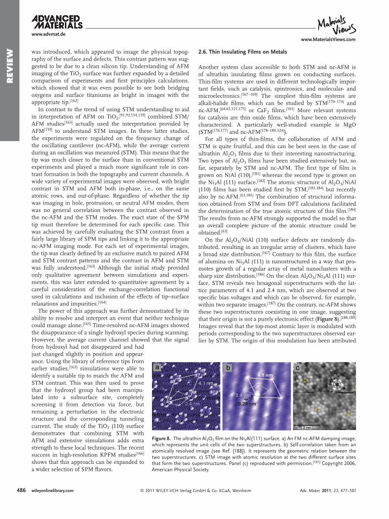
Figure 8 . The ultrathin Al 2 O 3 fi lm on the Ni 3 Al(111) surface. a) An FM nc-AFM damping image, which represents the unit cells of the two superstructures. b) Self-correlation taken from an atomically resolved image (see Ref. [ 188 ] ). It represents the geometric relation between the two superstructures. c) STM image with atomic resolution at the two different surface sites that form the two superstructures. Panel (c) reproduced with permission. [ 191 ] Copyright 2006, American Physical Society.
from hydroxyl had not disappeared and had just changed slightly in position and appear-ance. Using the library of reference tips from earlier studies, [ 163 ] simulations were able to identify a suitable tip to match the AFM and STM contrast. This was then used to prove that the hydroxyl group had been manipu-lated into a subsurface site, completely screening it from detection via force, but remaining a perturbation in the electronic structure and the corresponding tunneling current. The study of the TiO 2 (110) surface demonstrates that combining STM with AFM and extensive simulations adds extra strength to these local techniques. The recent success in high-resolution KPFM studies [ 166 ] shows that this approach can be expanded to a wider selection of SPM fl avors.
© 2011 WILEY-VCH Verlag Gmwileyonlinelibrary.com
2.6. Thin Insulating Films on Metals
Another system class accessible to both STM and nc-AFM is of ultrathin insulating fi lms grown on conducting surfaces. Thin-fi lm systems are used in different technologically impor-tant fi elds, such as catalysis, spintronics, and molecular- and microelectronics. [ 167 – 169 ] The simplest thin-fi lm systems are alkali-halide fi lms, which can be studied by STM [ 170–174 ] and nc-AFM, [ 64 , 65 , 121 , 175 ] or CaF 2 fi lms. [101] More relevant systems for catalysis are thin oxide fi lms, which have been extensively characterized. A particularly well-studied example is MgO (STM [ 176 , 177 ] and nc-AFM [ 178–180 , 324 ] ).
For all types of thin-fi lms, the collaboration of AFM and STM is quite fruitful, and this can be best seen in the case of ultrathin Al 2 O 3 fi lms due to their interesting nanostructuring. Two types of Al 2 O 3 fi lms have been studied extensively but, so far, separately by STM and nc-AFM. The fi rst type of fi lm is grown on NiAl (110), [ 181 ] whereas the second type is grown on the Ni 3 Al (111) surface. [ 182 ] The atomic structure of Al 2 O 3 /NiAl (110) fi lms has been studied fi rst by STM, [ 183 , 184 ] but recently also by nc-AFM. [ 63 , 185 ] The combination of structural informa-tion obtained from STM and from DFT calculations facilitated the determination of the true atomic structure of this fi lm. [ 184 ] The results from nc-AFM strongly supported the model so that an overall complete picture of the atomic structure could be obtained. [ 63 ]
On the Al 2 O 3 /NiAl (110) surface defects are randomly dis-tributed, resulting in an irregular array of clusters, which have a broad size distribution. [ 167 ] Contrary to this fi lm, the surface of alumina on Ni 3 Al (111) is nanostructured in a way that pro-motes growth of a regular array of metal nanoclusters with a sharp size distribution. [ 186 ] On the clean Al 2 O 3 /Ni 3 Al (111) sur-face, STM reveals two hexagonal superstructures with the lat-tice parameters of 4.1 and 2.4 nm, which are observed at two specifi c bias voltages and which can be observed, for example, within two separate images. [ 187 ] On the contrary, nc-AFM shows these two superstructures coexisting in one image, suggesting that their origin is not a purely electronic effect ( Figure 8 ). [ 188 , 189 ] Images reveal that the top-most atomic layer is modulated with periods corresponding to the two superstructures observed ear-lier by STM. The origin of this modulation has been attributed
bH & Co. KGaA, Weinheim Adv. Mater. 2011, 23, 477–501

www.advmat.dewww.MaterialsViews.com
REV
IEW
to a pinning of the oxide fi lm lattice on a supermesh, which is in coincidence with the atomic lattice of the Ni 3 Al substrate. [ 188 ] Quite recently, it has been shown that STM achieves atomic resolution on the fi lm. STM images show that the nodes of the 4.1 nm lattice correspond to holes in the fi lm. [ 191 ] Although this interpretation is supported by DFT calculations, [ 191 ] it has not yet been proven that the proposed fi lm structure is the most stable one.
The examples of alumina fi lms demonstrate yet again how collaboration between STM and nc-AFM aids the under-standing of surface structure by providing different, but com-plementary, information. For the Al 2 O 3 /Ni 3 Al (111) fi lm, a combination of STM and nc-AFM in a QPlus sensor setup [ 5 , 56 ] could be used in the future to fi nally resolve the true atomic structure. The combination of STM and nc-AFM provides a full set of images (topography, current, detuning, and damping) containing different types of tip–surface interactions to aid the atomic-structure analysis of the fi lm. This combination is not restricted to alumina fi lms, but can certainly be used for wider variety of thin insulating fi lms on metal and semiconductor substrates, opening new avenues in the atomic-structure anal-ysis of thin-fi lms.
2.7. Imaging Metallic Nanoclusters
Interest in studying metallic nanoparticles has increased rap-idly in the last decade, particularly due to the discovery of their surprising chemical activity when adsorbed on insulating substrates. [ 143 , 144 , 167 , 192 ] These nanocatalysts remain a topic of intense research, with many questions over the mechanisms of their reactivity still open. Since the insulating nature of many of the relevant substrates prevented the use of STM in most cases, AFM has become a common tool for local characteriza-tion of these systems.
Almost as soon as the technique became available, nc-AFM was also applied in studies of adsorbed nanoclusters: Au on alumina, [ 193 ] TiO 2 , [ 194 ] NaCl, [ 195 ] KBr, [ 196–201 ] RbI, [ 198 ] mica, [ 202 ]
© 2011 WILEY-VCH Verlag GmAdv. Mater. 2011, 23, 477–501
Figure 9 . Imaging clusters with the nc-AFM. a) A gold cluster on KBr (001corresponding image showing contrast in Δ f . The cluster has a size of a fewcluster (fuzzy object), is imaged. Only if the tip is close to the cluster, can a feimage (b) and constant-height image (c) of the same palladium clusters on image, is greatly reduced if the clusters are scanned in the constant-height mexemplifying the improvement in resolution. Panel (a) reproduced with perwith permission. [ 38 ] Copyright 2008, American Institute of Physics. Panel (Society.
MoS 2 , [229] poly-L-lysine coated mica, [ 203 ] Si, [ 204 ] InSb, [ 205 ] graphite [ 206 ] and gold; [ 206 ] Ag on graphite [ 207 ] and quartz; [ 208 ] Cu on alumina; [ 209 , 210 ] Pd on alumina [ 209 , 211 ] and MgO(001); [ 212 ] Ni on alumina; [ 213 ] Fe on NaCl; [ 214 ] Fe/Pt on NaCl; [ 214 , 215 ] InAs on GaAs; [ 202 ] Si on CaF 2 (111); [ 216 ] and Ge on Si. [ 217 , 218 ] In terms of resolution, many of these studies offered little benefi t over contact AFM measurements, [ 219–224 ] but the extra sensitivity improved the reproducibility of the measurements and reduced unintentional surface damage. Nanoclusters have been success-fully manipulated with nc-AFM, [ 202–204 , 225 ] but manipulation in the dynamic modes of AFM remains diffi cult and prone to oscillation instabilities due to the large forces involved.
One of the main aims of nc-AFM studies of nanoclusters on surfaces is to provide high resolution of both the cluster and the surface and ultimately to offer atomic scale details about sizes, shapes, and adsorption sites of the clusters. Efforts in this direction have generally focused on the relatively easy to prepare model systems, such as Au nanoclusters on alkali halide surfaces. [ 37 , 196 , 197 , 200 , 201 , 226 , 227 ] These studies often pro-vided atomic resolution on the insulating substrate. [ 196 , 200 ] However, at close approach nanoclusters are imaged only as fuzzy hemispheres, [ 196 , 200 ] hiding their true geometric shape [ 143 ] ( Figure 9 ). This is mainly due to the convolution of the tip with the nanocluster. [ 196 , 228 , 229 ] For small, nanometer-sized clusters the tip apex is effectively much larger and the shape of the tip apex is what is mostly imaged. [ 196 ] Signifi cant improvements in the resolution of nanoclusters can be achieved by imaging in the constant height mode, [ 37 ] where the tip convolution effect is greatly reduced (Figure 9 b–d). An extensive experimental and theoretical study of Pd nanoclusters on MgO (001) showed that the real shape of the clusters could be seen in constant height mode, independent of the shape of the tip. [ 38 ] None of these studies have demonstrated real atomic resolution of a nano-cluster, although careful approach to a nanocluster pinned at a step-edge has revealed some internal structure. [ 196 ]
Future studies will certainly push the resolution limits but, perhaps more importantly, an early success combining nano-cluster and molecular deposition [ 199 ] suggests that experiments
487bH & Co. KGaA, Weinheim wileyonlinelibrary.com 487
) imaged in the topography mode. Top: topography image, bottom: the nanometers, comparable to the tip radius, so that the tip, rather than the w details of the top facet of the cluster be imaged. Constant- Δ f topography
MgO (001). The tip–surface convolution, which appears in the topography ode. d) A constant-height image of copper clusters on bulk α -Al 2 O 3 (0001) mission. [ 196 ] Copyright 2004, Institute of Physics. Panels (b,c) reproduced d) reproduced with permission. [ 210 ] Copyright 2008, American Chemical
www.advmat.dewww.MaterialsViews.com
REV
IEW
488
toclaAttrpcpt
ip(itttictcnmnoemdrs
aNntpfcpinNMsCtmacawolt
will soon be able to look at products of molecular reactions on nanoclusters in atomic detail. Combined with the ability to look at charge transfer and polarization via KPFM [ 195 ] (see Section 3) and the use of STM for nanoclusters on thin insu-lating fi lms, [ 230 ] SPM offers a very powerful toolbox for studying these key systems.
2.8. Adsorbed Molecules and Atoms
The adsorption of atoms and molecules on insulating sur-faces is central to understanding catalysis, designing molec-ular electronics devices, and studying molecular magnetism. Through imaging topography, scanning probes can determine adsorption sites and the geometry of an adsorbed species and hence provide the understanding of their binding to a surface. Temperature-controlled measurements can give information regarding diffusion rates of adsorbates and their interaction with surface defects. Tip-induced manipulation can produce new structures and initiate chemical reactions. All these prop-erties have been studied on individual atoms and molecules at conducting surfaces using STM. [ 231 ] However, success ful appli-cation of nc-AFM in this area came much later. Since individual formate ions on the TiO 2 (110) surface have been imaged using FM nc-AFM some 15 years ago [ 153 ] and the combined STM/AFM studies of porphyrins on copper, [ 233 , 234 ] high-resolution studies on individual well-separated atoms and molecules are still rare. Theoretical calculations and experimental measure-ments [ 163 , 232,235 ] indicate that the tip–sample separation is usu-ally signifi cantly smaller during atomic-resolution imaging with nc-AFM rather than with STM. Hence, the interaction of the tip with weakly adsorbed atoms or molecules can change their position and confi guration or cause the adsorbate to be removed by the tip. [ 98 ] This makes atomically resolved nc-AFM imaging of individual species, as well as their controlled manip-ulation at surfaces, technically very challenging.
Determining the chemical adsorption site of a molecule usually requires simultaneously resolving both the adsorbed molecule and the atomic structure of the substrate. This is a challenge for both STM and AFM studies and requires the preparation of stable and sharp tips. Polar or metallic tips facilitate atomic resolution on ionic surfaces, [ 9 ] but such tips can also interact strongly with an adsorbed molecule and thus prevent stable imaging. To obtain reproducible, high-resolution imaging of both a surface and an adsorbed molecule, the tip should interact strongly with the surface atoms but not with the adsorbed molecule. Further, to determine an adsorption site from an experimental image, one needs to chemically identify the positions of individual surface atoms. Here, one possible strategy is to fi rst identify the ions or atoms of the surface in atomically resolved images, e.g., whether a bright spot in an image is a surface Na + or Cl − on NaCl (001), and then identify the adsorption site. This can be done by experimental observa-tions (see Section 2.4) and/or theoretical modeling of the tip–surface interaction (see Section 2.2). An alternative approach is to solve the inverse problem: one can use a theoretically pre-dicted adsorption site of an adsorbant (e.g., molecule or metal atom) and the image to chemically identify surface ions or atoms.
© 2011 WILEY-VCH Verlag Gmwileyonlinelibrary.com
An example of the fi rst approach is the determination of he adsorption sites of Au atoms on the alumina fi lm grown n NiAl (110). [ 185 ] The measurements were performed using a ombined nc-AFM/STM and metallic tip at 5 K. In this case the ow symmetry of the alumina fi lm helped to determine that Au toms preferentially bind to surface Al atoms located above an l atom of the NiAl substrate. Earlier studies used a combina-
ion of nc-AFM and KPFM to establish three different adsorp-ion sites of Pt atoms on the TiO 2 (110)-(1x1) surface. [ 236 ] More ecent studies used the earlier understanding of the contrast atterns of the substrate to establish the adsorption sites and onfi gurations of cytosine on the CaF 2 (111) surface, [ 237 ] and erylene derivatives [ 238 ] ( Figure 10 a) and terephthalic acid [ 239 ] on he TiO 2 (110) surface.
The second approach has been used in nc-AFM studies of ndividual molecules of Co-Salen (Figure 10 b), a small chiral aramagnetic metal-organic Schiff base complex, on the NaCl 001) surface using Cr-coated tips at 30 K. [ 240 , 241 ] The obtained mages simultaneously exhibit both the position and the orien-ation of the adsorbed molecules and the atomic structure of he surface, enabling the determination of the exact adsorp-ion site. Density functional theory calculations were used to dentify the ionic sublattice resolved with the Cr tip and also to onfi rm the adsorption site and orientation of the molecule on he surface. Imaging molecules at room temperature is more hallenging. Custom-designed syn-5,10,15-tris(4-cyanophe-ylmethyl) truxene molecules were imaged with atomic and olecular resolution at room temperature using nc-AFM at the
anoscale structured KBr (001) surface. [ 242 ] The molecules were bserved rapidly diffusing along the perfect monolayer step dges and immobilized at monolayer kink sites. Extensive ato-istic simulations elucidate the mechanisms of adsorption and
iffusion of the molecule on the different surface features. The esults of this study suggest methods of controlling the diffu-ion of adsorbates on insulating and nanostructured surfaces.
A different approach has been used to image pentacene with tomic resolution using nc-AFM/STM on patches of ultrathin aCl layers deposited on Cu (111) at 5 K. [ 64 ] In this system, tun-elling is still possible and suitable tips could be prepared on
he bare metallic substrate in the STM mode using standard rocedures to transfer certain atomic or molecular species rom the surface to the tip apex. [ 243 ] Such well-controlled pro-edures currently do not exist for pure nc-AFM measurements, articularly not on bulk insulating surfaces. A tip functional-
zed with a CO molecule in this manner was then used in the c-AFM mode to image pentacene molecules adsorbed on the aCl islands with submolecular resolution (Figure 10 c–h). odeling played a vital role in determining the mechanism of
ubmolecular resolution resulting from the interaction of the O-terminated tip and pentacene, with the authors concluding
hat Pauli repulsion is the main source of atomic contrast in the olecular image. This approach has been later used to provide
detailed chemical model for a previously misassigned mole-ule, cephalandole A. [ 244 ] Similarly, nc-AFM investigations of dsorbed molecules on mica and TiO 2 surfaces [ 245 , 246 ] combined ith theoretical modeling suggest that the repulsive regime f contrast formation can be identifi ed and controlled by ana-yzing origins of contrast inversion in images. This goes beyond he common perception that the best and most non-invasive
bH & Co. KGaA, Weinheim Adv. Mater. 2011, 23, 477–501

www.advmat.dewww.MaterialsViews.com
REV
IEW
Figure 10 . nc-AFM images of a) perylene adsorbed on TiO 2 (110), b) Co-salen adsorbed on NaCl and pentacene adsorbed on thin NaCl fi lms on copper using different tip terminations. c,d) CO molecule, e) Ag, f) CO, g) Cl, and h) pentacene. Panel (a) reproduced with permission. [ 237 ] Copyright 2009, American Physical Society. Panel (b) reproduced with permission. [ 240 ] Copyright 2009, Institute of Physics. Panels (c–h) reproduced with permission. [ 64 ] Copyright 2009, American Association for the Advancement of Science.
contrast can be achieved in the attractive regime of tip–surface interaction.
Controlled manipulation of atoms and molecules with nc-AFM tips is now becoming a reality. [ 10, 33 ] Signifi cant suc-cess has been achieved at semiconductor surfaces since the earliest publications. [ 247–249 ] Despite several theoretical studies
© 2011 WILEY-VCH Verlag GmAdv. Mater. 2011, 23, 477–501
Figure 11 . Examples of atomically resolved nc-AFM experimental images in liquid. a) 2D and b) 3D images of the mica surface in water. c) Calcite (10-14) surface in water. d) Dipalmitoylphosphatidylcholine (DPPC) lipid bilayer in a phosphate buffer saline (PBS) solution. Panel (a) adapted with permission. [ 272 ] Copyright 2010, American Physical Society. Panel (b) adapted with permission. [ 86 ] Copyright 2010, American Physical Society. Panel (c) adapted with permission. [ 273 ] Copyright 2009, American Chem-ical Society. Panel (d) adapted with permission. [ 274 ] Copyright 2007, American Physical Society.
suggesting that manipulating atoms at insulating surfaces should be feasible, [ 250–252 ] experimental breakthroughs proved much more diffi cult to achieve. Tip-induced displacements of atom-sized defects on a CaF 2 (111) surface at room temperature have been observed [ 98 ] and similar results have been obtained on the KCl (100) surface. [ 253 ] In these studies, the defects were dragged by the nc-AFM tip along the slow-scan direction at given threshold tip–surface distances. However, achieving con-trolled manipulation still requires achieving much better con-trol over the tip structure and the balance of forces between the tip, the surface, and the manipulated species.
2.9. Imaging in Air and Liquids
Although many of the recent success stories of AFM have been achieved in UHV conditions, for most applications this is not a particularly relevant environment, e.g., studies in air or ambient gases would be more relevant for catalysis [ 143 ] and studies in liquid would mimic the physiological conditions relevant to biological systems. [ 48 ] Furthermore, controlling the environment offers the possibility of damping van der Waals interactions and removing capillary forces. [ 254 ] Of course, the fi rst AFM studies were in air [ 255 , 256 ] and some early high-resolu-tion studies were in water. [ 41 ] In these studies, AFM is operated in contact mode and suffers from similar problems to studies of systems in UHV in contact, i.e., the imaging process is inva-sive and the large lateral tip–surface forces damage or deform the sample. Recent contact studies have improved on this, [ 257 ] but it is particularly a problem in organic or biological systems, where molecules are often only physisorbed to the surface by
489bH & Co. KGaA, Weinheim wileyonlinelibrary.com 489

www.advmat.dewww.MaterialsViews.com
REV
IEW
490
weak van der Waals interactions. Imaging these systems is pos-sible if the molecules are fi rmly attached to the surface or form a crystal structure, [ 69 , 258–263 ] but even for high-resolution studies on predominantly fl at surfaces, [ 41 ] in contact mode it is very dif-fi cult to understand whether AFM really sees the surface or just a convolution of surface, tip, and liquid molecules.
A natural route to reduce the lateral forces experienced by the sample is to reduce the amount of time the tip spends in contact by introducing vertical cantilever motion. [ 34 ] Instead of contacting the surface throughout the scan, the tip only con-tacts the surface gently at the closest approach of the oscil-lating cantilever. A mode of AFM operation using amplitude modulation (AM) (see Section 2.1) is known as tapping mode or intermittent contact. [ 264 ] It has proven very successful for imaging samples in liquid, [ 7 , 265–267 ] and its capability for high-resolution studies in physiological conditions has led to AFM becoming the tool of choice for the investigation of biological systems. [ 48 , 268 ] However, its ultimate resolution is limited to the nanometer level by the low quality factor of the cantilever reso-nance in air and liquid environments causing high noise. [ 34 , 269 ] The same problem prevents conventional FM-AFM in air and liquids from offering comparable resolution to that commonly seen in UHV. For a standard microfabricated silicon cantilever, the Q factor is 10 000–200 000 in vacuum, 300–600 in air, and 1–20 in liquid; molecular resolution is estimated to be pos-sible down to Q values of around a few hundred. [ 270 ] Despite reduced viscosity, imaging in inert gases offers similar quality to imaging in air, with a Q value of about 500 using conven-tional amplitudes. [ 271 ]
It was recognized fairly early in the development of FM-AFM that stiffer cantilevers and small amplitudes could offer dramatic increases in the signal-to-noise ratio and Q. [ 49 ] Generally, low-amplitude, stiff cantilevers are fabricated from quartz tuning forks and appropriate tips are glued to the end of a beam, [ 55 , 56 , 275 ] but stiff metal cantilevers have also been used. [ 276 ] Despite increased diffi culty in preparation, low-amplitude studies have been very successful in UHV atomic-resolution studies of sev-eral insulating surfaces and thin fi lms, [ 61 , 102 , 178 , 277 , 278 ] and have also been used to study water nanoclusters on mica in air. [ 279 ] Even conventional silicon cantilevers can be operated at low amplitude and this has proved to be a breakthrough in high-resolution imaging in liquids. [ 270 , 273,280 , 281 ] Using ultrasmall amplitudes of tenths of a nanometer, the low Q outside UHV
Figure 12 . Objects of different chemical compositions exhibit differences in the local work function on the surface (metal) or in the electrostatic surface potential (insulators), which can be used for the chemical identifi cation in AFM.
is compensated and lateral resolution of a few hundred picometers was achieved in water on molecular crystals, [ 280,281 ] mica, [ 272 ] and a lipid bilayer (see Figure 11). [ 274 ] Refi ne-ments in sensitivity offer the potential for an order of magnitude improvement in resolu-tion [ 282 ] and the use of small cantilevers could improve this further. Recent developments in speed and control mean it is possible to perform 3D imaging in water, and this was applied to obtain unprecedented resolution of the structure of water layers on mica. [ 86 ] Beyond FM-AFM, phase modulation can signifi cantly improve the imaging speed in liquids [ 283 ] and oscillating the cantilever lat-erally in torsional resonance mode [ 284 , 285 ]
© 2011 WILEY-VCH Verlag Gwileyonlinelibrary.com
again increases sensitivity and has been successfully applied to studies in liquids. [ 286 ] Most recently, small-amplitude AM-AFM has demonstrated high resolution of a wide variety of substrates in liquid conditions. [ 287 ]
In the future, molecular and atomic resolution in air and liq-uids is certain to become almost routine and greater efforts will be made in interpretation and understanding the infl uence of the environment on both the measurement and the sample. In this direction, combining SPM techniques will again be a pow-erful approach, with the capabilities of the electrostatic map-ping that KPFM would offer in characterizing biomolecules in physiological conditions being particularly promising.
3. Long-Range Electrostatic Forces in AFM
As discussed above, one can rarely determine the chemical nature of surface atoms or supported nano-objects from imaging the surface topography alone. In most cases, a com-bination of experiment and theory (see Section 2.2), doping crystals with known impurities (see Section 2.4), or deco-rating surface sites with known adsorbates (see Section 2.8) are needed to achieve unambiguous chemical identifi cation. It has long been realized that measuring the long-range electro-static forces may assist chemical identifi cation . As illustrated in Figure 12 , nano–objects of different chemical composition (metal or insulating fi lms, ions, molecules, etc.) change the local electrostatic surface potential by changing the local work function of a metal surface. [ 288 – 292 ] Such nano–objects also change the local electrostatic potential when supported on an insulating surface. Measuring the local work function or elec-trostatic potential of a surface by AFM with a resolution in the mV range and at the nanometer scale could be used for chem-ical identifi cation of surface species. Apart from other electro-static AFMs like electrostatic force microscopy (see Table 1 and references therein), this can be achieved using KPFM, which has become a well-established surface science tool in many sci-entifi c disciplines. [ 23 , 24 , 293 ]
KPFM is a very effective technique for directly measuring the contact potential difference between the conducting tip and conducting surface. [ 21 , 22 ] In such a measurement, a direct cur-rent (dc) ( U dc ) and an alternating current (ac) voltage ( U ac ) with frequency f ac are applied between the tip and surface. Owing to
mbH & Co. KGaA, Weinheim Adv. Mater. 2011, 23, 477–501

www.advmat.dewww.MaterialsViews.com
REV
IEW
the modulation of the electrostatic force by the ac voltage, the electrostatic contribution, oscillating at frequency f ac and also at 2 f ac , can be extracted (fi rst and second harmonic). The fi rst har-monic includes a term with U dc + U CPD , in which U CPD is the contact potential difference between tip and surface. By varying the dc voltage such that the fi rst harmonic becomes zero ( U dc = – U CPD ), the total electrostatic tip–surface interaction is mini-mized at each point on the surface. The contact potential differ-ence between the tip and surface is then given by U dc = – U CPD = ( ϕ sample – ϕ tip )/ e where ϕ sample and ϕ tip are the work functions of the sample and tip, respectively and e is the electron charge. At two different locations on the surface (positions 1 and 2), the difference ( U dc,pos1 – U dc,pos2 ) e = ( ϕ pos1 – ϕ tip ) – ( ϕ pos2 – ϕ tip ) = ϕ pos1 – ϕ pos2 = Δ ϕ yields the work function difference between these locations.
In most cases the Kelvin modulation technique is applied during normal nc-AFM topography imaging. Depending on the ac frequency, one distinguishes between frequency- [ 294 ] and amplitude-modulated [ 295 ] KPFM (see also Refs. [ 296 , 297 ] ). An independent feedback loop regulates the dc voltage so that U dc = – U CPD is achieved at each point on the surface. Both topography and a so-called Kelvin image of U dc = – U CPD are obtained at the same time in one measurement, where the Kelvin contrast corresponds to local variations of the surface work function. If insulating surfaces are imaged, fi xed charges or dipoles, which change the local electrostatic surface poten-tial, determine the contrast in the Kelvin image. [ 298 – 300 ] In the literature many different aspects of the Kelvin technique can be found. [ 21 − 23 , 294 – 297 , 301 – 303 ] Below we present several examples of recent KPFM applications, which deal with metal–insulator interfaces and defects at insulating surfaces.
3.1. Thin Insulating Films on Conducting Surfaces
A convenient way to study insulating surfaces is to prepare a thin insulating fi lm on a conducting support. On such fi lms, charging experiments can be performed, where charges can be created by different methods with the tip: contacting the tip with the surface, by corona discharge from the tip, or by inducing tunneling of electrons from the conducting sup-port into the thin-fi lm or vice versa. Most experiments of this type were done in air by EFS and EFM on SiO 2 , [ 304 ] Si 2 N 3 , [ 305 ] Al 2 O 3 , [ 306 , 307 ] GaN, [ 308 ] and PMMA [ 309 ] fi lms and also on nano-
© 2011 WILEY-VCH Verlag GmAdv. Mater. 2011, 23, 477–501
Figure 13 . KPFM on thin-fi lms. a–c) NaCl fi lms on Cu (111) (topography (the different layers of NaCl (0: Cu, 1–3: 1–3 ML NaCl). d,e) Perylene-3,4,9,10KBr on Ag (111). If PTCDA is located on 1ML KBr, clusters and rods are formBoth types of molecular fi lms exhibit large differences in the work function opermission. [ 320 ] Copyright 2009, Institute of Physics. Panels (d,e) reproduce
clusters embedded into or supported by thin SiO 2 fi lms. [ 310 – 313 ] In UHV, such experiments can be more precise, such that single electron processes can be studied. [ 299 , 314 ]
An important application of KPFM is to measure work func-tion changes of conducting supports induced by adsorbed thin insulating fi lms, which can be best realized under the clean conditions of UHV. In most cases, thin insulating fi lms are prepared in such a way that they only partially cover a con-ducting surface, so that the work function difference between the conducting support and the fi lm can be directly imaged by the Kelvin microscope ( Figure 13 ). Spectroscopic measure-ments [ 315– 317 ] and theoretical calculations [ 289 , 290 , 292 , 318 ] demon-strate that NaCl, KBr, or MgO thin-fi lms lower the work func-tion of metal substrates. This work function change has been quantitatively measured at the nanoscale by KPFM for LiCl, NaCl, KCl, and RbCl fi lms on Au (111); [ 319 ] for NaCl and KBr fi lms on Cu (111); [ 320 ] for KBr fi lms on Ag (111); [ 321 ] and for MgO thin-fi lms on Ag (001). [ 180 , 324 ] The lowering of the sur-face work function has also been found on semiconductor substrates, e.g., in the case of KBr (001) thin-fi lms on InSb (001). [ 322 , 323 ]
A very important issue is whether KPFM on thin insulating fi lms can achieve high lateral resolution and accurately measure a work function difference between a fi lm and a conducting support. Although a change in the surface work function at a fi lm–support boundary can be observed with nanometer resolu-tion, [ 320 ] the work function plateaus only at very large distances from the boundary. In fact, in most cases work function dif-ferences are correctly measured at distances of 50–100 nm from the boundary. [ 297 , 319 , 320 , 323 ] As the electrostatic tip–surface interaction is of long-range character, the size of the whole tip apex is then responsible for the accuracy of the work function measurements. The importance of this effect has been clearly demonstrated on one-layer-thick MgO (001) islands grown on Ag (001); the effective radius of the tip apex is often larger than the 5–10-nm-large islands and the work function difference has much smaller values than expected. [ 324 ] However, tip changes occur quite frequently in such experiments, which leads occa-sionally to a sharp, neutral nanotip at the apex and, in turn, to a better representation of true work function differences. [ 180 ]
Insulating thin-fi lms are also important buffer layers in molecular electronics, where molecules are electronically decoupled from the conducting support by the thin-fi lm. Since the coupling between the conducting support and the
491bH & Co. KGaA, Weinheim wileyonlinelibrary.com 491
a) and corresponding Kelvin image (c)). The drawing in panel (b) shows -tetracarboxylic-3,4,9,10-dianhydride (PTCDA) on 1 and 2 monolayer (ML) ed (topography image (d)). On 2ML KBr, a closed regular fi lm is formed.
f the Ag (111) surface (see Kelvin image e). Panels (a–c) reproduced with d with permission. [ 321 ] Copyright 2006, Institute of Physics.

www.advmat.dewww.MaterialsViews.com
REV
IEW
492
molecules varies with the thickness of the insulating fi lm, the electronic properties, such as the work function, of such heter-ostructures can be tailored. This effect has been quantitatively imaged using KPFM for PTCDA and Alq 3 molecules adsorbed on the KBr (001)/Au (111) surface. [ 321 , 325 ] These measurements exhibit clear differences in the surface work function if mol-ecules are supported either on the gold surface or on one- or two-monolayer-thick KBr (001) islands (Figure 13 d,e).
The recent progress in nc-AFM using functionalized tips and a combination of STM and nc-AFM on molecules sup-ported on thin-fi lms shows that each atom of a molecule can be imaged. [ 64 ] Besides the atomic structure, the electronic proper-ties of a molecule are also important. By scanning tunneling spectroscopy, the electronic states close to the Fermi level can be probed. [ 326 , 327 ] On the other hand, inelastic tunneling spec-troscopy is able to measure vibrational properties of the mol-ecule. [ 326 , 327 ] Here, KPFM measurements could provide addi-tional information on the local surface work function at the molecule and on the presence of extra charges or dipoles inside the molecule.
In the case of metal nanoclusters on ultrathin fi lms, KPFM could be used to image directly charge transfer between the conducting support and nanoclusters, which has been pre-dicted by theory [ 290 , 292 , 318 , 328 ] and experimentally observed by spectroscopy methods and STM on MgO thin fi lms. [ 318 , 381 ] Furthermore, the tip can be used to intentionally charge single nanoclusters and to afterwards observe the charge evolution from the cluster into the support as a function of time, which is important for applications in nanotechnology and surface chemistry.
3.2. Individual Defects on Bulk Insulating Surfaces
Defects of atomic size, such as vacancies, play an important role in the chemistry of insulating surfaces. As most of these defects are chemically active, their characterization can only be done in UHV. One can attempt to identify defects by combining nc-AFM and KPFM as follows: the surface and defects are fi rst imaged with high- or even atomic-resolution by nc-AFM, then Kelvin microscopy is performed at the same position on the surface. Images with atomic resolution supply information on the atomic structure of the surface, whereas the Kelvin images yield information about the charge state (sign and strength) of the surface defects. With this, and the knowledge of the mate-rial’s properties, it is possible to determine the electronic state and, under specifi c circumstances, the chemical nature of the considered defects.
Defect identifi cation by KPFM has fi rst been demonstrated on semiconductor surfaces. For instance, topography images of the UHV-cleaved p-WSe 2 (0001) surface exhibit a very faint con-trast of small defects on the terraces, whereas corresponding Kelvin images show a bright or dark Kelvin contrast at these places. [ 329 ] Due to the Kelvin contrast, such defects can be iden-tifi ed as negative (bright) and positive (dark) dopants, which would not be possible to conclude from the topography images alone. Similar observations have been made on p- and n-type doped SiO 2 fi lms on Si (111), [ 330 ] on UHV cleaved n- and p-type doped GaAs (110), and on p-type doped GaP (110) surfaces. [ 331 ]
© 2011 WILEY-VCH Verlag Gmwileyonlinelibrary.com
On the latter surfaces, large differences in the Kelvin contrast at steps have been observed and assigned to a downward and upward band bending due to localized charged dopants.
Recently, it has been shown that KPFM can also yield valu-able information for the identifi cation of defects at surfaces of bulk insulators, such as the (001) surfaces of bulk alkali-halide crystals. An important question is what KPFM is actually meas-uring on an insulating surface. In KPFM, an external poten-tial is applied between the tip and the metallic sample holder and the electrostatic fi eld penetrates the insulator. The Kelvin microscope measures then the contact potential difference between the tip and the sample holder, which is modifi ed by the insulator between the tip and sample holder. [ 20 ] The valence and conduction bands of the insulator are usually positioned such that the Fermi level of the metallic sample holder is in the band gap of the insulator. [ 332 ] However, because the (001) surfaces of alkali-halide or MgO crystals are mostly prepared by in situ cleavage, [ 50 ] a signifi cant region below the new sur-face is damaged due to the large uncontrolled stress that is applied during the cleavage. This produces defects in the bulk and especially at the surface, many of which are charged. As a result, the sample is charged, strongly infl uencing the Kelvin voltage, [ 18 ] and shifts of tens of volts have been measured by KPFM. [ 50 , 52 , 333 ]
Surface charging after cleavage hampers imaging with high resolution. [ 50 , 52 , 333 ] To avoid this, in situ cleaved alkali-halide or MgO crystals are usually annealed at high temperatures prior to AFM experiments to remove most of the charge. After achieving an equilibrium charge state by annealing, a faint contrast at the defects is observed in KPFM images due to residual charges on the surface. [ 52 ] In the case of alkali-halide surfaces, bright patches at steps correspond to a more negative surface poten-tial in comparison to the neutral and stoichiometric terraces. At each patch, nc-AFM imaging with atomic resolution reveals single atomic-sized defects, which are located at kinks and cor-ners of steps [ 300 ] ( Figure 14 ). In fact, such measurements are in perfect agreement with the model of the surface double layer (Debye-Frenkel layer), [ 334 , 335 ] where alkali-halide surfaces have a negative net surface charge at room temperature. [ 336– 339 ] The negative charge is due to the negative cation vacancies at kinks and corners, [ 340 ] which locally change the electrostatic surface potential. A similar mechanism can be found at dislocations, which are also reservoirs of positive or negative defects. [ 335 ] Recent KPFM and atomic-resolution imaging on KBr (001) have proven the existence of charged vacancies at dislocations and an identifi cation of the defects could be made [ 341 ] ( Figure 15 ).
A net negative surface charge was also observed at Suzuki pre-cipitates on Cd 2 + - and Mg 2 + -doped NaCl crystal surfaces, [ 134 , 135 ] resulting from the negative cation vacancies inside the Suzuki structure. On MgO (001), the net surface charge was found to be negative, [ 212 ] contrary to the expected presence of positive F + or F 2 + centers on the MgO (001) surface. [ 342 , 343 ] Despite an occa-sional dark Kelvin contrast at some places on the surface due to the possible presence of F centers, it was concluded that most of the F centers have probably reacted with the residual gas in the UHV, forming negative species such as charged O 2 − or CO − radicals at low coordinated surface sites. [ 328 ]
These few examples show that KPFM helps in identifying charged surface defects, which is not possible from nc-AFM
bH & Co. KGaA, Weinheim Adv. Mater. 2011, 23, 477–501

www.advmat.dewww.MaterialsViews.com
REV
IEW
Figure 14 . The surface double layer (Debye-Frenkel layer) on ionic crystal surfaces. The topo graphy image (a) shows a step, at which bright patches can be seen in the Kelvin image (b). Atomic-resolution imaging in the constant height mode (c) reveals a kink at each bright patch (compare positions 1–3). The bright patches in the Kelvin image are a result of negative cation vacancies, which are located at the kinks and which pro-duce a more negative surface potential with respect to the perfect and neutral terraces. The images were recorded on the NaCl (001) surface. Reproduced with permission. [ 300 ] Copyright 2006, American Chemical Society.
topography images alone. The sensitivity of KPFM is suffi -ciently high to detect charges with an equivalent amount of less than one electron. [ 298 , 300 , 344 ] This provides the possibility to use a combination of nc-AFM and KPFM also on other surfaces. Candidates for the future are ionic crystal surfaces like the (111) surfaces of fl uorites, oxide surfaces, and even more com-plex surfaces. A challenge is to apply nc-AFM and KPFM on surfaces where atomic resolution has not yet been well under-stood. For instance, the (111) surface of CeO 2 exhibits a variety of point defects, which still urgently need identifi cation. [ 103 ]
A further important challenge is achieving atomic resolu-tion in KPFM. A few examples already exist where atomic resolution could be obtained, and reasonable understanding has been achieved for ideal ionic [ 345– 347 ] and more complex surfaces. [ 348 , 349 ] Moving beyond this to understanding high-resolution images of defects, thin fi lms, molecules, and clusters still requires signifi cant efforts. However, these efforts are strongly motivated by the demonstrated poten-tial of KPFM to capture electrostatic changes due to local-ized charging and chemical reactions in a wide variety of systems. [ 350 , 351 ]
3.3. Metal Nanoclusters on Insulating Surfaces
Another major challenge of KPFM is characterizing supported nano-objects, such as metal clusters. Metal nanoclusters on insulating oxide surfaces play a particularly important role in catalysis by promoting many chemical reactions; [ 143 , 144 ] a marked
© 2011 WILEY-VCH Verlag GmAdv. Mater. 2011, 23, 477–501
example is the oxidation of CO on Au/TiO 2 . [ 352 ] Recently it has been realized that a support can change the electronic and, therefore, the catalytic properties of the clusters. [ 144 ] This has been shown to be crucial, for example, in the case of ultrathin MgO (001) fi lms, [ 289–291 , 353 , 354 , 381 ] where supported gold clusters become charged by the metal support beneath the insulating fi lm. Since charge transfer modifi es the electronic structure and related properties, such as the work function of large clus-ters, KPFM is a promising technique for studying charging of individual clusters with nanometer resolution. In the fol-lowing, large clusters are defi ned as those containing at least 1000 atoms. For such clusters the ionization potential equals the work function of the bulk material. [ 355 ]
Simple surfaces demonstrating KPFM works quite effi ciently are conducting surface systems (e.g., metal clusters or fi lms on metal surfaces), which have been studied in air [ 312 , 356– 359 ] and also in UHV. [ 205 , 294 , 296 ] KPFM can accurately probe work func-tion differences between large clusters and a substrate surface with a lateral resolution at the nanometer scale and with the energy sensitivity in the mV range. This has been tested by growing gold clusters on graphite. [ 296 ] or on silicon. [ 294 ] Such work function measurements can even reveal an alloying between the substrate and the clusters, as has been observed on Au/InSb(001) [ 205 ]
On the surfaces of bulk insulators, KPFM has been mainly used to study metal clusters on alkali halide and MgO crystal surfaces. In such experiments, the bulk insulator separates the clusters from a conducting support (metallic sample holder), so that no conducting channels exist between the clusters and the support. This aspect is important especially when charge is transferred between a cluster and the tip during contact. The charge stays for a very long time on the cluster and electrons can be transferred only to the neighboring clusters located at nano-meter-scale distances from the charged cluster [ 195 ] ( Figure 16 a,b). When clusters are neutral on the insulating surface, KPFM measures the work function difference between the insulator on the conducting sample holder and large clusters. [ 212 ] How-ever, in most cases, the clusters are infl uenced by the insulating support, which has be observed for gold clusters on alkali-halide surfaces, [ 195 ] palladium clusters on MgO (001) [ 212 ] (Figure 16 c), or even for single platinum atoms on the TiO 2 (110) surface. [ 236 , 360 ]
The resolution in KPFM images of large clusters is greatly enhanced and provides a more accurate measure of the cluster work function in comparison with that of thin insu-lating fi lms (Figure 16 d,e)) [ 212 ] This is because the tip is usu-ally several nanometers away from the insulating surface when placed above a cluster (this distance is close to the height of the cluster), so that the electrostatic tip–surface interaction is mainly due to the tip–cluster interaction.
The few existing examples demonstrate that KPFM can indeed image the electronic properties of cluster–surface sys-tems at the nanometer scale. One can thus perform KPFM studies on many other cluster–surface systems, including deposited molecules. [ 201 ] An important challenge is to study very small nanoclusters (e.g., deposited gas-phase clusters), which contain only up to a hundred atoms. Such clusters exhibit strong variations in the ionization potential, which changes drastically if only one atom is added to or removed from the cluster. [ 144 , 355 ] Differences in the electronic properties
493bH & Co. KGaA, Weinheim wileyonlinelibrary.com 493

www.advmat.dewww.MaterialsViews.com
REV
IEW
494
Figure 15 . Dislocations on the KBr (001) surface studied by KPFM (a: topography, b: Kelvin image). The topography image (a) shows a string of shallow hillocks emerging from the surface. At the end of one hillock, atomic resolution imaging (c) reveals an edge dislocation, which Burgers vector is represented by the circuit drawn on (c) representing the direction [1 − 10] and magnitude of the vector ( √ 2a/2). Thanks to the bright Kelvin contrast (b), the defects could be identifi ed as nega-tive defects. Reproduced with permission. [ 341 ] Copyright 1995, American Physical Society.
amongst such small clusters can also be expected if the clusters are supported on a surface, which could be verifi ed by high-resolution KPFM.
As discussed above, a big benefi t of AFM in general, is that the tip can be used to explicitly charge metal clusters and then to study the charge state with electrostatic AFMs. The reliability of controlled charging by the AFM tip has been already shown
© 2011 WILEY-VCH Verlag Gmwileyonlinelibrary.com
Figure 16 . a,b) Gold clusters on NaCl (001) after a contact of the tip with ondistance of 2.8 nm, charges propagated along cluster rows in an area of 30a strong contrast could be observed due to a strong Coulomb interaction wcontrast at the clusters shows that groups of clusters exhibit different contrasubstrate. d,e) Similar Pd clusters grown on MgO (001). The lateral resolutCopyright 2006, American Institute of Physics. Panels (d,e) reproduced with
in EFM experiments, [ 310–313 ] but KPFM should be able to achieve further progress in such experiments due to its much higher lat-eral resolution and better energy sensitivity. Due to the charge sensitivity of the KPFM down to an equivalent charge of one electron and below [ 300 , 305 ] and to the capability to inject a single electron into a single atom, [ 171 ] controlled charging experiments of clusters via the AFM tip and characterization by KPFM are within reach.
The biggest promise of KPFM is related to surface chem-istry because the classical Kelvin probe already allows one to follow chemical reactions on surfaces by monitoring changes of the surface work function. [ 13 , 14 ] Preliminary results obtained on Pd/graphite demonstrate that the KPFM is indeed chemically sensitive. [ 361 ] For instance, the contami-nation of the clusters by constituents of the residual gas at 10 − 10 mbar can be followed on a time scale of some hours ( Figure 17 , upper panel). Immediately following preparation, the Pd clusters exhibit a bright Kelvin contrast (Figure 17 , middle panel), which is due to their higher work function with respect to HOPG. On a timescale of one week, the work function of the Pd clusters drops below the value of HOPG (dark contrast) because of a chemical reaction with the residual gas in the UHV. A high-temperature anneal of the contaminated Pd clusters in oxygen cleans the Pd clusters so that they again exhibit their initial work function (Figure 17 , bottom panel). Although the clusters are quite large, size and site effects can be already observed: smaller clusters are more reactive than larger clusters and edges or facets of clusters exhibit a different potential than the top facet of the clusters. These KPFM measurements strongly motivate the use of KPFM as a standard local probe technique for work function measurements of cluster–surface systems of interest in sur-face chemistry.
4. Outlook
Advances in STM have long allowed insight into the mecha-nisms and rates of adsorption, diffusion, and reactions on conducting surfaces by directly observing the motions of the individual atoms and molecules involved. However, it is only recently that nc-AFM started catching up with its sister tech-nique in this part of its application spectrum. With rapid
bH & Co. KGaA, Weinheim Adv. Mater. 2011, 23, 477–501
e of the clusters (see arrow in panel (a)). Due to the small cluster–cluster 0 × 300 nm. In both the Kelvin image (b) and the topography image (a) ith the tip. c) Kelvin image of Pd clusters on MgO (001). The increased st due to different possible charge transfers between the clusters and the ion is approximately 5 nm. Panels (a–c) reproduced with permission. [ 195 ] permission. [ 212 ] Copyright 2004, Institute of Physics.
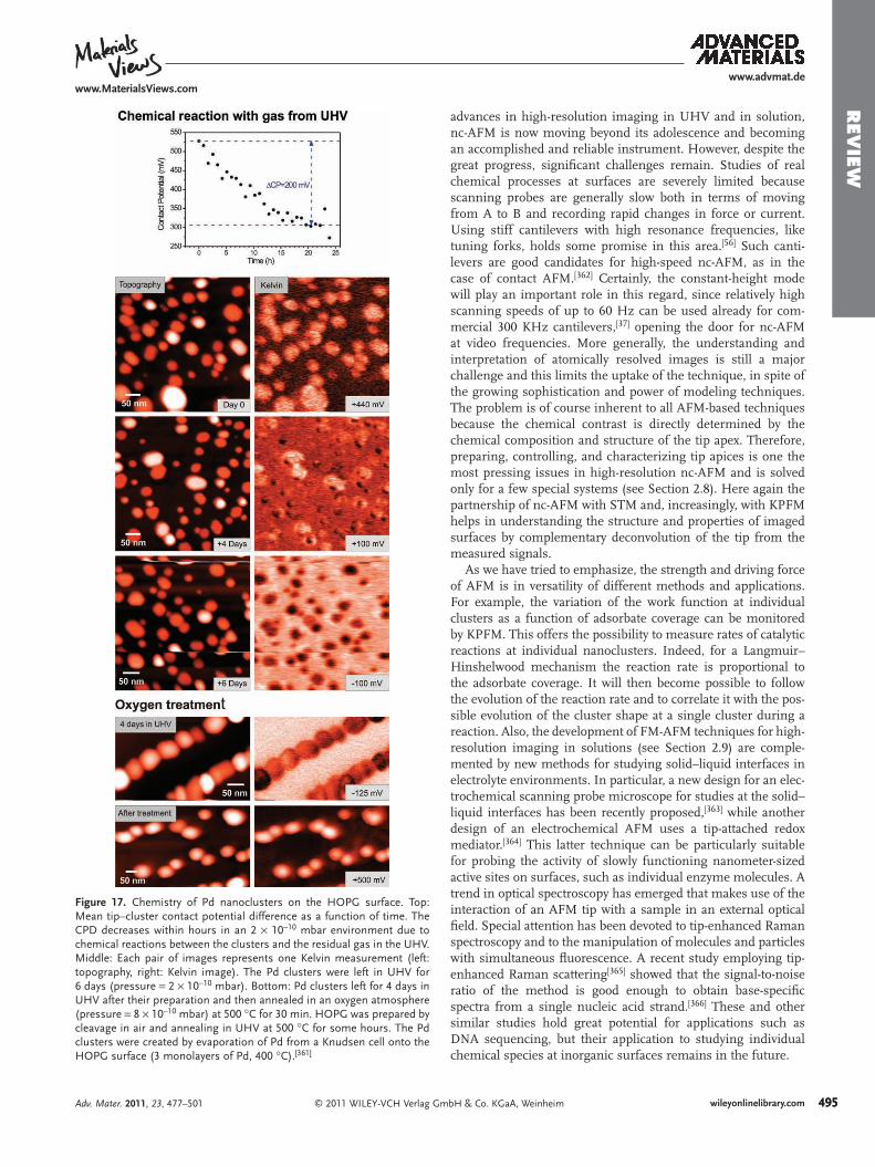
www.advmat.dewww.MaterialsViews.com
REV
IEW
© 2011 WILEY-VCH Verlag GmAdv. Mater. 2011, 23, 477–501
Figure 17 . Chemistry of Pd nanoclusters on the HOPG surface. Top: Mean tip–cluster contact potential difference as a function of time. The CPD decreases within hours in an 2 × 10 − 10 mbar environment due to chemical reactions between the clusters and the residual gas in the UHV. Middle: Each pair of images represents one Kelvin measurement (left: topography, right: Kelvin image). The Pd clusters were left in UHV for 6 days (pressure = 2 × 10 − 10 mbar). Bottom: Pd clusters left for 4 days in UHV after their preparation and then annealed in an oxygen atmosphere (pressure = 8 × 10 − 10 mbar) at 500 ° C for 30 min. HOPG was prepared by cleavage in air and annealing in UHV at 500 ° C for some hours. The Pd clusters were created by evaporation of Pd from a Knudsen cell onto the HOPG surface (3 monolayers of Pd, 400 ° C). [ 361 ]
advances in high-resolution imaging in UHV and in solution, nc-AFM is now moving beyond its adolescence and becoming an accomplished and reliable instrument. However, despite the great progress, signifi cant challenges remain. Studies of real chemical processes at surfaces are severely limited because scanning probes are generally slow both in terms of moving from A to B and recording rapid changes in force or current. Using stiff cantilevers with high resonance frequencies, like tuning forks, holds some promise in this area. [ 56 ] Such canti-levers are good candidates for high-speed nc-AFM, as in the case of contact AFM. [ 362 ] Certainly, the constant-height mode will play an important role in this regard, since relatively high scanning speeds of up to 60 Hz can be used already for com-mercial 300 KHz cantilevers, [ 37 ] opening the door for nc-AFM at video frequencies. More generally, the understanding and interpretation of atomically resolved images is still a major challenge and this limits the uptake of the technique, in spite of the growing sophistication and power of modeling techniques. The problem is of course inherent to all AFM-based techniques because the chemical contrast is directly determined by the chemical composition and structure of the tip apex. Therefore, preparing, controlling, and characterizing tip apices is one the most pressing issues in high-resolution nc-AFM and is solved only for a few special systems (see Section 2.8). Here again the partnership of nc-AFM with STM and, increasingly, with KPFM helps in understanding the structure and properties of imaged surfaces by complementary deconvolution of the tip from the measured signals.
As we have tried to emphasize, the strength and driving force of AFM is in versatility of different methods and applications. For example, the variation of the work function at individual clusters as a function of adsorbate coverage can be monitored by KPFM. This offers the possibility to measure rates of catalytic reactions at individual nanoclusters. Indeed, for a Langmuir–Hinshelwood mechanism the reaction rate is proportional to the adsorbate coverage. It will then become possible to follow the evolution of the reaction rate and to correlate it with the pos-sible evolution of the cluster shape at a single cluster during a reaction. Also, the development of FM-AFM techniques for high-resolution imaging in solutions (see Section 2.9) are comple-mented by new methods for studying solid–liquid interfaces in electrolyte environments. In particular, a new design for an elec-trochemical scanning probe microscope for studies at the solid–liquid interfaces has been recently proposed, [ 363 ] while another design of an electrochemical AFM uses a tip-attached redox mediator. [ 364 ] This latter technique can be particularly suitable for probing the activity of slowly functioning nanometer-sized active sites on surfaces, such as individual enzyme molecules. A trend in optical spectroscopy has emerged that makes use of the interaction of an AFM tip with a sample in an external optical fi eld. Special attention has been devoted to tip-enhanced Raman spectroscopy and to the manipulation of molecules and particles with simultaneous fl uorescence. A recent study employing tip-enhanced Raman scattering [ 365 ] showed that the signal-to-noise ratio of the method is good enough to obtain base-specifi c spectra from a single nucleic acid strand. [ 366 ] These and other similar studies hold great potential for applications such as DNA sequencing, but their application to studying individual chemical species at inorganic surfaces remains in the future.
495bH & Co. KGaA, Weinheim wileyonlinelibrary.com 495

www.advmat.dewww.MaterialsViews.com
REV
IEW
496
The application of force microscopies to technological prob-lems is also expanding and often requires the combination of several methods. In particular, scanning capacitance micro-scopy (SCM) and scanning spreading resistance microscopy (SSRM) are used for implant mapping, whereas conductive AFM (C-AFM) is used for the analysis of thin dielectrics and KPFM is used to study the potential distribution across active electronic devices. [ 367 ] AFM can be also used as a part of nano-optomechanical device, where mechanical changes on the nanometer scale control the optical properties of artifi cial struc-tures. In a recent study of a gold bow-tie nanoantenna with var-iable feedback, the gap was tuned by nanomanipulation with an AFM tip and the optical resonances were measured with dark-fi eld scattering spectroscopy. [ 368 ]
We hope that this paper demonstrates that the fi eld of force microscopy is very much alive, and new techniques and appli-cations are developing rapidly. New material and environment combinations are being included into the realm of SPM high-resolution imaging on a regular basis. Combined with advances in the speed of scanning and chemical identifi cation, the future will see many diverse fi elds and applications opened to this powerful suite of techniques.
Acknowledgements We are grateful to Ezra Bussman, Jeppe Lauritsen and Alexander Schwarz for critical reading of the manuscript. This work was supported by the European COST program through Action D41. CB, ASF and CRH acknowledge support from the European Science Foundation through the FANAS network. ASF acknowledges support from the Academy of Finland through its Centre of Excellence program. ALS acknowledges support from the FP6 IP PICO-inside and from the Leverhulme Trust.
Received: June 23, 2010 Revised: August 20, 2010
Published online: November 11, 2010
[ 1 ] E. Meyer , H. J. Hug , R. Bennewitz , Scanning probe microscopy: the lab on a tip , Springer-Verlag , Berlin, 2004 .
[ 2 ] Forces in scanning probe methods , (Eds: H. J. Güntherodt, D. Anselmetti, E. Meyer), Springer-Verlag , Berlin 1995 .
[ 3 ] L. Howald , H. Haefke , R. Lüthi , E. Meyer , G. Gerth , H. Rudin , H.-J. Güntherodt , Phys. Rev. B 1994 , 49 , 5651 .
[ 4 ] F. J. Giessibl , Science 1995 , 267 , 68 . [ 5 ] F. J. Giessibl , Rev. Mod. Phys. 2003 , 75 , 949 . [ 6 ] T. R. Albrecht , P. Grütter , D. Horne , D. Rugar , J. Appl. Phys. 1991 ,
69 , 668 . [ 7 ] R. García , R. Pérez , Surf. Sci. Rep. 2002 , 47 , 197 . [ 8 ] Noncontact Atomic Force Microscopy , (Eds: S. Morita , R. Wiesendanger ,
E. Meyer ) Springer , Berlin 2002 . [ 9 ] W. Hofer , A. S. Foster , A. L. Shluger , Rev. Mod. Phys. 2003 , 75 , 1287 . [ 10 ] Noncontact Atomic Force Microscopy Volume 2 , (Eds: S. Morita ,
F. J. Giessibl , R. Wiesendanger ), Springer , Berlin 2010 . [ 11 ] L. Kelvin , G. Fitzgerald , W. Francis , Philos. Mag. J. Sci. 1898 , 46 ,
82 . [ 12 ] W. A. Zisman , Rev. Sci. Instrum. 1932 , 3 , 367 . [ 13 ] G. Ertl , P. R. Norton , J. Rüstig , Phys. Rev. Lett. 1982 , 49 , 177 . [ 14 ] S. Ladas , R. Imbihl , G. Ertl , Surf. Sci. 1989 , 219 , 88 . [ 15 ] M. Schmidt , M. Nohlen , G. Bermes , M. Böhmer , K. Wandelt , Rev.
Sci. Instrum. 1997 , 68 , 3866 .
© 2011 WILEY-VCH Verlag Gmwileyonlinelibrary.com
[ 16 ] J. Fiasson , O. B. Harris , J. Phys. E: Sci. Instrum. 1977 , 10 , 1160 . [ 17 ] L. B. Harris , J. Fiasson , J. Phys. E: Sci. Instrum. 1984 , 17 , 788 . [ 18 ] L. B. Harris , J. Fiasson , J. Phys. C: Solid State Phys. 1985 , 18 , 4845 . [ 19 ] L. B. Harris , J. Phys. C: Solid State Phys. 1987 , 20 , 5677 . [ 20 ] G.-N. Luo , K. Yamaguchi , T. Terai , M. Yamawaki , J. Alloys Compd.
2003 , 349 , 211 . [ 21 ] J. M. R. Weaver , D. W. Abraham , J. Vac. Sci. Technol. B 1991 , 9 ,
1559 . [ 22 ] M. Nonnenmacher , M. P. O Boyle , H. K. Wickramasinghe , Appl.
Phys. Lett. 1991 , 58 , 2921 . [ 23 ] P. Girard , Nanotechnology 2001 , 12 , 485 . [ 24 ] R. Berger , H. J. Butt , M. B. Retschke , S. A. L. Weber , Macromol.
Rapid Commun. 2009 , 30 , 485 . [ 25 ] A. S. Foster , W. A. Hofer , Scanning Probe Microscopes: Atomic scale
engineering by forces and currents , Springer , Berlin 2006 . [ 26 ] D. A. Bonnell , Probe Microscopy and Spectroscopy: Theory and Tech-
niques and Applications , Wiley-VCH , Berlin 2000 . [ 27 ] F. J. Giessibl , Jpn. J. Appl. Phys. 1994 , 33 , 3726 . [ 28 ] R. A. Oliver , Rep. Prog. Phys. 2008 , 71 , 076501 . [ 29 ] D. A. Bonnell , J. Garra , Rep. Prog. Phys. 2008 , 71 , 044501 . [ 30 ] J. V. Lauritsen , M. Reichling , J. Phys.: Condens. Matter 2010 , 22 ,
263001 . [ 31 ] E. I. Altman , U. D. Schwarz , Adv. Mater. 2010 , 22 , 2854 . [ 32 ] Y. Gan , Surf. Sci. Rep. 2009 , 64 , 99 . [ 33 ] Ó. Custance , R. Perez , S. Morita , Nat. Nanotechnol. 2009 , 4 , 803 . [ 34 ] Y. Martin , C. C. Williams , H. K. Wickramasinghe , J. Appl. Phys.
1987 , 61 , 4723 . [ 35 ] Q. Zhong , D. Inniss , K. Kjoller , V. B. Elings , Surf. Sci. Lett. 1993 ,
290 , L688 . [ 36 ] C. Barth , A. S. Foster , M. Reichling , A. L. Shluger , J. Phys.: Condens.
Matter 2001 , 13 , 2061 . [ 37 ] C. Barth , O. H. Pakarinen , A. S. Foster , C. R. Henry , Nanotechnology
2006 , 17 , S128 . [ 38 ] H. Pakarinen , C. Barth , A. S. Foster , C. R. Henry , J. Appl. Phys. 2008 ,
103 , 054313 . [ 39 ] G. Couturier , R. Boisgard , D. Dietzel , J. P. Aimé , Nanotechnology
2005 , 16 , 1346 . [ 40 ] R. J. Driscoll , M. G. Youngquist , J. D. Baledschwieler , Nature 1990 ,
346 , 294 . [ 41 ] F. Ohnesorge , G. Binnig , Science 1993 , 260 , 1451 . [ 42 ] A. Engel , D. J. Müller , Nat. Struct. Biol. 2000 , 7 , 715 . [ 43 ] K. D. Jandt , Surf. Sci. 2001 , 491 , 303 . [ 44 ] P. J. James , M. Antognozzi , J. Tamayo , T. J. McMaster ,
J. M. Newton , M. J. Miles , Langmuir 2001 , 17 , 349 . [ 45 ] T. Aoki , Y. Sowa , H. Yokota , M. Hiroshima , M. Tokunaga , Y. Ishii ,
T. Yanagida , Single Mol. 2001 , 2 , 183 . [ 46 ] A. Philippsen , W. Im , A. Engel , T. Schirmer , B. Roux , D. J. Müller ,
Biophys. J. 2002 , 82 , 1667 . [ 47 ] G. Kada , F. Kienberger , P. Hinterdorfer , Nano Today 2008 , 3 , 12 . [ 48 ] D. J. Müller , Y. F. Dufrene , Nat. Nanotechnol. 2008 , 3 , 261 . [ 49 ] F. J. Giessibl , H. Bielefeldt , S. Hembacher , J. Mannhart , Appl. Surf.
Sci. 1999 , 140 , 352 . [ 50 ] C. Barth , C. Claeys , C. R. Henry , Rev. Sci. Instrum. 2005 , 76 , 083907 . [ 51 ] R. Bennewitz , M. Bammerlin , M. Guggisberg , C. Loppacher ,
A. Baratoff , E. Meyer , H.-J. Güntherodt , Surf. Interface Anal. 1999 , 27 , 462 .
[ 52 ] C. Barth , C. R. Henry , Nanotechnology 2006 , 17 , S155 . [ 53 ] Y. Ma , A. S. Foster , R. M. Nieminen , J. Chem. Phys. 2005 , 122 ,
144709 . [ 54 ] M. A. Lantz , H. J. Hug , R. Hoffmann , S. Martin , A. Baratoff ,
H. J. Güntherodt , Phys. Rev. B 2003 , 68 , 035324 . [ 55 ] H. Edwards , L. Taylor , W. Duncan , J. Appl. Phys. 1997 , 82 , 980 . [ 56 ] F. J. Giessibl , Appl. Phys. Lett. 1998 , 73 , 3956 . [ 57 ] T. Eguchi , Y. Hasegawa , Phys. Rev. Lett. 2002 , 89 , 266105 .
bH & Co. KGaA, Weinheim Adv. Mater. 2011, 23, 477–501

www.advmat.dewww.MaterialsViews.com
REV
IEW
[ 58 ] F. J. Giessibl , S. Hembacher , H. Bielefeldt , J. Mannhart , Science 2000 , 289 , 422 .
[ 59 ] S. M. Langkat , H. Hölscher , A. Schwarz , R. Wiesendanger , Surf. Sci. 2003 , 527 , 12 .
[ 60 ] U. Kaiser , A. Schwarz , R. Wiesendanger , Nature 2007 , 446 , 522 . [ 61 ] M. Schmid , J. Mannhart , F. J. Giessibl , Phys. Rev. B 2008 , 77 ,
045402 . [ 62 ] M. Ternes , C. P. Lutz , C. F. Hirjibehedin , F. J. Giessibl , A. J. Heinrich ,
Science 2008 , 319 , 1066 . [ 63 ] G. H. Simon , T. Koenig , M. Nilius , H. P. Rust , M. Heyde ,
H. J. Freund , Phys. Rev. B 2008 , 78 , 113401 . [ 64 ] L. Gross , F. Mohn , N. Moll , P. Liljeroth , G. Meyer , Science 2009 ,
325 , 1110 . [ 65 ] L. Gross , F. Mohn , P. Liljeroth , J. Repp , F. J. Giessibl , G. Meyer ,
Science 2009 , 324 , 1428 . [ 66 ] M. Ara , A. Sasahara , H. Onishi , H. Tada , Nanotechnology 2004 , 15 ,
S65 . [ 67 ] D. Takamatsu , Y. Yamakoshi , K. Fukui , J. Phys. Chem. B 2006 , 110 ,
1968 . [ 68 ] H. Dai , J. H. Hafner , A. G. Rinzler , D. T. Colbert , R. E. Smalley ,
Nature 1996 , 384 , 147 . [ 69 ] S. P. Jarvis , T. Uchihashi , T. Ishida , H. Tokumoto , Y. Nakayama ,
J. Phys. Chem. B 2000 , 104 , 6091 . [ 70 ] R. Wilson , V. Macpherson , Nat. Nanotechnol. 2009 , 4 , 483 . [ 71 ] A. I. Livshits , A. L. Shluger , A. Rohl , A. S. Foster , Phys. Rev. B. 1999 ,
59 , 2436 . [ 72 ] R. Pérez , M. C. Payne , I. Stich , K. Terakura , Phys. Rev. Lett. 1997 ,
78 , 678 . [ 73 ] Y. Sugimoto , P. Pou , M. Abe , P. Jelinek , R. Pérez , S. Morita ,
Ó. Custance , Nature 2007 , 446 , 64 . [ 74 ] B. J. Albers , T. C. Schwendemann , M. Z. Baykara , N. Pilet ,
M. Liebmann , E. I. Altman , U. D. Schwarz , Nat. Nanotechnol. 2009 , 4 , 307 .
[ 75 ] M. A. Lantz , H.-J. Hug , P. J. A. Schendel , R. Hoffmann , S. Martin , A. Baratoff , A. Abdurixit , H. J. Güntherodt , Ch. Gerber , Phys. Rev. Lett. 2000 , 84 , 2642 .
[ 76 ] M. A. Lantz , H.-J. Hug , R. Hoffman , P. J. A. Schendel , P. Kappenberger , S. Martin , A. Baratoff , H.-J. Güntherodt , Science 2001 , 291 , 2580 .
[ 77 ] P. Pou , S. A. Ghasemi , P. Jelinek , T. Lenosky , S. Goedecker , R. Perez , Nanotechnology 2009 , 20 , 264015 .
[ 78 ] W. Allers , A. Schwarz , U. D. Schwarz , R. Wiesendanger , Rev. Sci. Instrum. 1998 , 69 , 221 .
[ 79 ] H.-J. Hug , B. Stiefel , P. J. A. Schendel , A. Moser , S. Martin , H.-J. Güntherodt , Rev. Sci. Instrum. 1999 , 70 , 3625 .
[ 80 ] R. Hoffmann , M. A. Lantz , H.-J. Hug , P. J. A. van Schendel , P. Kappenberger , S. Martin , A. Baratoff , H. -J. Güntherodt , Phys. Rev. B 2003 , 67 , 085402 .
[ 81 ] R. Hoffmann , L. N. Kantorovich , A. Baratoff , H.-J. Hug , H.-J. Güntherodt , Phys. Rev. Lett 2004 , 92 , 146103 .
[ 82 ] R. Hoffmann , C. Barth , A. S. Foster , A. L. Shluger , H.-J. Hug , H.-J. Güntherodt , R. M. Nieminen , M. Reichling , J. Am. Chem. Soc. 2005 , 127 , 17863 .
[ 83 ] M. Abe , Y. Sugimoto , Ó. Custance , S. Morita , Appl. Phys. Lett. 2005 , 87 , 173503 .
[ 84 ] M. Abe , Y. Sugimoto , Ó. Custance , S. Morita , Nanotechnology 2005 , 16 , 3029 .
[ 85 ] G. M. King , A. R. Carter , A. B. Churnside , L. S. Eberle , T. T. Perkins , Nano Lett. 2009 , 9 , 1451 .
[ 86 ] T. Fukuma , Y. Ueda , S. Yoshioka , H. Asakawa , Phys. Rev. Lett. 2010 , 104 , 016101 .
[ 87 ] H. Hölscher , S. M. Langkat , A. Schwarz , R. Wiesendanger , Appl. Phys. Lett. 2002 , 81 , 4428 .
[ 88 ] M. Z. Baykara , T. C. Schwendemann , E. I. Altman , U. D. Schwarz , Adv. Mater. 2010 , 22 , 2838 .
© 2011 WILEY-VCH Verlag GmAdv. Mater. 2011, 23, 477–501
[ 89 ] N. Oyabu , P. Pou , Y. Sugimoto , P. Jelinek , M. Abe , S. Morita , R. Pérez , O. Custance , Phys. Rev. Lett. 2006 , 96 , 106101 .
[ 90 ] C. Lazo , V. Caciuc , H. Hölscher , S. Heinze , Phys. Rev. B 2008 , 78 , 214416 .
[ 91 ] K. I. Fukui , H. Onishi , Y. Iwasawa , Chem. Phys. Lett. 1997 , 280 , 296 .
[ 92 ] M. Ashino , Y. Sugawara , S. Morita , M. Ishikawa , Phys. Rev. Lett. 2001 , 86 , 4334 .
[ 93 ] S. Hembacher , F. Giessibl , J. Mannhart , C. Quate , Phys. Rev. Lett. 2005 , 94 , 056101 .
[ 94 ] A. S. Foster , C. Barth , A. L. Shluger , M. Reichling , Phys. Rev. Lett. 2001 , 86 , 2373 .
[ 95 ] A. S. Foster , C. Barth , A. L. Shluger , R. M. Nieminen , M. Reichling , Phys. Rev. B 2002 , 66 , 235417 .
[ 96 ] Sh. Fujii , M. Fujihira , Nanotechnology 2006 , 17 , S112 . [ 97 ] S. Fujii , M. Fujihira , Jpn. J. Appl. Phys. 2006 , 45 , 1986 . [ 98 ] S. Hirth , F. Ostendorf , M. Reichling , Nanotechnology 2006 , 17 ,
S148 . [ 99 ] S. Fujii , M. Fujihira , Nanotechnology 2007 , 18 , 084011 . [ 100 ] A. S. Foster , T. Trevethan , A. L. Shluger , Phys. Rev. B 2009 , 80 , 115421 . [ 101 ] A. Klust , T. Ohta , A. Bostwick , Q. Yu , F. Ohuchi , M. Olmstead ,
Phys. Rev. B 2004 , 69 , 035405 . [ 102 ] J. Giessibl , M. Reichling , Nanotechnology 2005 , 16 , S118 . [ 103 ] S. Torbrügge , M. Reichling , A. Ishiyama , S. Morita , Ó. Custance ,
Phys. Rev. Lett. 2007 , 99 , 56101 . [ 104 ] S. Torbrügge , M. Cranney , M. Reichling , Appl. Phys. Lett. 2008 , 93 ,
073112 . [ 105 ] K. Fukui , S. Takakusagi , R. Tero , M. Aizawa , Y. Namai , Y. Iwasawa ,
Phys. Chem. Chem. Phys. 2003 , 5 , 5349 . [ 106 ] S. Gritschneder , Y. Namai , Y. Iwasawa , M. Reichling , Nanotech-
nology 2005 , 16 , S41 . [ 107 ] S. Gritschneder , M. Reichling , J. Phys. Chem. C 2008 , 112 , 2045 . [ 108 ] S. Gritschneder , M. Reichling , Nanotechnology 2007 , 18 , 044024 . [ 109 ] S. Gritschneder , Y. Iwasawa , M. Reichling , Nanotechnology 2007 ,
18 , 044025 . [ 110 ] C. Barth , C. R. Henry , Phys. Rev. Lett. 2003 , 91 , 196102 . [ 111 ] J. V. Lauritsen , M. C. R. Jensen , K. Venkataramani , B. Hinnemann ,
S. Helveg , B. S. Clausen , F. Besenbacher , Phys. Rev. Lett. 2009 , 103 , 076103 .
[ 112 ] F. Ostendorf , C. Schmitz , S. Hirth , A. Kühnle , J. J. Kolodziej , M. Reichling , Langmuir 2009 , 25 , 10764 .
[ 113 ] F. Ostendorf , S. Torbruegge , M. Reichling , Phys. Rev. B 2008 , 77 , 041405 .
[ 114 ] E. Palacios-Lidon , O. Grauby , C. Henry , J. P. Astier , C. Barth , A. Baronnet , Am. Mineral 2010 , 95 , 673 .
[ 115 ] M. Nimmrich , M. Kittelmann , P. Rahe , A. J. Mayne , G. Dujardin , A. von Schmidsfeld , M. Reichling , W. Harneit , A. Kühnle , Phys. Rev. B 2010 , 81 , 201403 .
[ 116 ] C. Barth , M. Reichling , Nature 2001 , 414 , 54 . [ 117 ] S. Torbruegge , F. Ostendorf , M. Reichling , J. Phys. Chem. C 2009 ,
113 , 4909 . [ 118 ] F. Ostendorf , C. Schmitz , S. Hirth , A. Kühnle , J. J. Kolodziej ,
M. Reichling , Nanotechnology 2008 , 19 , 305705 . [ 119 ] J. Schütte , Ph. Rahe , L. Troeger , S. Rode , R. Bechstein ,
M. Reichling , A. Kühnle , Langmuir 2010 , 26 , 8295 . [ 120 ] M. Bammerlin , R. Lüthi , E. Meyer , J. Lü , M. Guggisberg , Ch. Loppacher ,
C. Gerber , H.-J. Güntherodt , Appl. Phys. A 1998 , 66 , S293 . [ 121 ] R. Bennewitz , A. S. Foster , L. N. Kantorovich , M. Bammerlin ,
Ch. Loppacher , S. Schär , M. Guggisberg , E. Meyer , A. L. Shluger , Phys. Rev. B 2000 , 62 , 2074 .
[ 122 ] R. Bennewitz , O. Pfeiffer , S. Schär , V. Barwich , E. Meyer , L. N. Kantorovich , Appl. Surf. Sci. 2002 , 188 , 232 .
[ 123 ] M. A. Cerda , J. Abad , A. Madgavkar , D. Martrou , S. Gauthier , Nano-technology 2008 , 19 , 045503 .
[ 124 ] F. Seitz , Rev. Mod. Phys. 1946 , 18 , 384 .
497bH & Co. KGaA, Weinheim wileyonlinelibrary.com 497

www.advmat.dewww.MaterialsViews.com
REV
IEW
498
[ 125 ] F. Seitz , Rev. Mod. Phys. 1954 , 26 , 7 . [ 126 ] W. Hayes , A. M. Stoneham , Defects and defect processes in
nonmetallic solids , Wiley-Interscience , New York 1985 . [ 127 ] L. N. Kantorovich , A. L. Shluger , A. M. Stoneham , Phys. Rev. Lett.
2000 , 85 , 3846 . [ 128 ] H. E. Carrillo , H. A. Carrillo , O. J. Rubio , Phys. Status Solidi 1987 ,
101 , 315 . [ 129 ] K. Suzuki , J. Phys. Soc. Jpn. 1961 , 16 , 67 . [ 130 ] C. J. J. Van Loon , D. J. W. Ijdo , Acta Cryst. B 1975 , 31 , 770 . [ 131 ] M. Chall , B. Winkler , P. Blaha , K. Schwarz , J. Phys. Chem. B 2000 ,
104 , 1191 . [ 132 ] A. L. Guerrero , E. P. Butler , P. L. Pratt , L. W. Hobbs , Philos. Mag. A
1981 , 43 , 1359 . [ 133 ] M. J. Yacamán , Phys. Status Solidi B 1973 , 56 , 429 . [ 134 ] C. Barth , C. R. Henry , New J. Phys. 2009 , 11 , 043003 . [ 135 ] C. Barth , C. R. Henry , Phys. Rev. Lett. 2008 , 100 , 96101 . [ 136 ] A. S. Foster , C. Barth , C. R. Henry , Phys. Rev. Lett. 2009 , 102 ,
256103 . [ 137 ] G. A. Bassett , M. J. Yacamán , Thin Solid Films 1976 , 31 , 375 . [ 138 ] P. Aceituno , F. Cussó , A. De Andrés , F. Jaque , Solid State Commun.
1984 , 49 , 209 . [ 139 ] C. Cros , L. Hanebali , L. Latié , G. Villeneuve , W. Gang , Solid State
Ionics 1983 , 9–10 , 139 . [ 140 ] E. Lilley , J. B. Newkirk , J. Mat. Sci. 1967 , 2 , 567 . [ 141 ] S. Kasper , J. S. Prenner , Acta Cryst. 1953 , 7 , 246 . [ 142 ] P. Porta , G. Minelli , I. L. Botto , E. J. Baran , J. Solid State Chem.
1991 , 92 , 202 . [ 143 ] C. R. Henry , Surf. Sci. Rep. 1998 , 31 , 231 . [ 144 ] U. Heiz , U. Landman , Nanocatalysis , Springer Verlag , Berlin
2007 . [ 145 ] R. Bechstein , M. Kitta , J. Schütte , A. Kühnle , H. Onishi , J. Phys.
Chem. C 2009 , 113 , 13199 . [ 146 ] R. Bechstein , M. Kitta , J. Schütte , A. Kühnle , H. Onishi , J. Phys.
Chem. C 2009 , 113 , 3277 . [ 147 ] A. L. Linsebigler , G. Lu , J. T. Yates , Chem. Rev. 1995 , 95 , 735 . [ 148 ] V. E. Henrich , P. A. Cox , The Surface Science of Metal Oxides ,
Cambridge University Press , Cambridge 1996 . [ 149 ] J. Lausmaa , J. Electron Spectosc. Relat. Phenom. 1996 , 81 , 343 . [ 150 ] J. Ni , K. H. Leung , Y. C. Leung , K. Sumathy , Renewable Sustainable
Energy Rev. 2007 , 11 , 401 . [ 151 ] U. Diebold , Surf. Sci. Rep. 2003 , 48 , 53 . [ 152 ] U. Diebold , J. F. Anderson , K. O. Ng , D. Vanderbilt , Phys. Rev. Lett.
1996 , 77 , 1322 . [ 153 ] K. I. Fukui , H. Onishi , Y. Iwasawa , Phys. Rev. Lett. 1997 , 79 , 4202 . [ 154 ] M. Ashino , T. Uchihashi , K. Yokoyama , Y. Sugawara , S. Morita ,
M. Ishikawa , Appl. Surf. Sci. 2000 , 157 , 212 . [ 155 ] S. H. Ke , T. Uda , K. Terakura , Phys. Rev. B 2002 , 65 , 125417 . [ 156 ] A. S. Foster , O. H. Pakarinen , J. M. Airaksinen , J. D. Gale ,
R. M. Nieminen , Phys. Rev. B 2003 , 68 , 195410 . [ 157 ] A. S. Foster , A. Y. Gal , J. M. Airaksinen , O. H. Pakarinen , Y. J. Lee ,
J. D. Gale , A. L. Shluger , R. M. Nieminen , Phys Rev. B 2003 , 68 , 195420 .
[ 158 ] A. S. Foster , A. Y. Gal , J. D. Gale , Y. J. Lee , R. M. Nieminen , A. L. Shluger , Phys. Rev. Lett. 2004 , 92 , 036101 .
[ 159 ] J. V. Lauritsen , A. S. Foster , G. H. Olesen , M. C. Christensen , A. Kühnle , S. Helveg , J. R. Rostrup-Nielsen , B. S. Clausen , M. Reichling , F. Besenbacher , Nanotechnology 2006 , 17 , 3436 .
[ 160 ] S. Wendt , R. Schaub , J. Matthiesen , E. K. Vestergaard , E. Wahlström , M. D. Rasmussen , P. Thostrup , L. M. Molina , E. Lægsgaard , I. Stensgaard , B. Hammer , F. Besenbacher , Surf. Sci. 2005 , 598 , 226 .
[ 161 ] G. H. Enevoldsen , A. S. Foster , M. C. Christensen , J. V. Lauritsen , F. Besenbacher , Phys. Rev. B 2007 , 76 , 205415 .
[ 162 ] R. Bechstein , C. Schütte , J. Gonzalez , P. Jelinek , R. Perez , A. Kühnle , Nanotechnology 2009 , 20 , 505703 .
© 2011 WILEY-VCH Verlag Gwileyonlinelibrary.com
[ 163 ] G. H. Enevoldsen , H. P. Pinto , A. S. Foster , M. C. R. Jensen , A. Kühnle , M. Reichling , W. A. Hofer , J. V. Lauritsen , F. Besenbacher , Phys. Rev. B 2008 , 78 , 45416 .
[ 164 ] H. P. Pinto , H. Enevoldsen , F. Besenbacher , A. S. Foster , J. V. Lauritsen , Nanotechnology 2009 , 20 , 264020 .
[ 165 ] G. H. Enevoldsen , H. P. Pinto , A. S. Foster , M. C. R. Jensen , W. A. Hofer , B. Hammer , J. V. Lauritsen , F. Besenbacher , Phys. Rev. Lett. 2009 , 102 , 136103 .
[ 166 ] G. H. Enevoldsen , T. Glatzel , M. C. Christensen , J. V. Lauritsen , F. Besenbacher , Phys. Rev. Lett. 2008 , 100 , 236104 .
[ 167 ] J. Libuda , H.-J. Freund , Surf. Sci. Rep. 2005 , 57 , 157 . [ 168 ] M. S. Chen , D. W. Goodman , J. Phys.: Condens. Matter 2008 , 20 ,
264013 . [ 169 ] M. E. Vaida , T. M. Bernhardt , C. Barth , F. Esch , U. Heiz ,
U. Landman , Phys. Status Solidi B 2010 , 247 , 1001 . [ 170 ] J. Repp , S. Fölsch , G. Meyer , K. H. Rieder , Phys. Rev. Lett. 2001 , 86 ,
252 . [ 171 ] J. Repp , G. Meyer , F. E. Olsson , M. Persson , Science 2004 , 305 ,
493 . [ 172 ] M. Pivetta , F. Patthey , M. Stengel , A. Baldereschi , W.-D. Schneider ,
Phys. Rev. B 2005 , 72 , 115404 . [ 173 ] J. Repp , G. Meyer , S. Paavilainen , F. E. Olsson , M. Persson , Science
2006 , 312 , 1196 . [ 174 ] P. Liljeroth , J. Repp , G. Meyer , Science 2007 , 317 , 1203 . [ 175 ] T. Filleter , W. Paul , R. Bennewitz , Phys. Rev. B 2008 , 77 , 8 . [ 176 ] S. Schintke , S. Messerli , M. Pivetta , F. Patthey , L. Libioulle ,
M. Stengel , A. De Vita , W.-D. Schneider , Phys. Rev. Lett. 2001 , 87 , 276801 .
[ 177 ] M. Sterrer , M. Heyde , M. Novicki , N. Nilius , T. Risse , H. P. Rust , G. Pacchioni , H. J. Freund , J. Phys. Chem. B 2006 , 110 , 46 .
[ 178 ] M. Heyde , M. Sterrer , H. P. Rust , H.-J. Freund , Appl. Phys. Lett. 2005 , 87 , 083104 .
[ 179 ] M. Heyde , G. H. Simon , H. P. Rust , H.-J. Freund , Appl. Phys. Lett. 2006 , 89 , 263107 .
[ 180 ] M. Bieletzki , T. Hynninen , T. M. Soini , M. Pivetta , C. R. Henry, A. S. Foster , F. Esch , C. Barth , U. Heiz , Phys. Chem. Chem. Phys. 2010 , 12 , 3203 .
[ 181 ] J. Libuda , F. Winkelmann , M. Bäumer , H.-J. Freund , T. Bertrams , H. Neddermeyer , K. Müller , Surf. Sci. 1994 , 318 , 61 .
[ 182 ] C. Becker , K. von Bergmann , A. Rosenhahn , J. Schneider , K. Wandelt , Surf. Sci. 2001 , 486 , L443 .
[ 183 ] M. Kulawik , N. Nilius , H. P. Rust , H.-J. Freund , Phys. Rev. Lett. 2003 , 91 , 256101 .
[ 184 ] G. Kresse , M. Schmid , E. Napetschnig , M. Shishkin , L. Kohler , P. Varga , Science 2005 , 308 , 1440 .
[ 185 ] G. H. Simon , T. König , H. -P. Rust , M. V. Ganduglia-Pirovano , J. Sauer , M. Heyde , H.-J. Freund , Phys. Rev. B 2010 , 81 , 073411 .
[ 186 ] G. Hamm , C. Becker , C. R. Henry , Nanotechnology 2006 , 17 , 1943 .
[ 187 ] A. Rosenhahn , J. Schneider , C. Becker , K. Wandelt , J. Vac. Sci. Technol. A 2000 , 18 , 1923 .
[ 188 ] G. Hamm , C. Barth , C. Becker , K. Wandelt , C. R. Henry , Phys. Rev. Lett. 2006 , 97 , 126106 .
[ 189 ] S. Gritschneder , C. Becker , K. Wandelt , M. Reichling , J. Am. Chem. Soc 2007 , 129 , 4925 .
[ 190 ] H. Brune , M. Giovannini , K. Bromann , K. Kern , Nature 1998 , 394 , 451 .
[ 191 ] M. Schmid , G. Kresse , A. Buchsbaum , E. Napetschnig , S. Gritschneder , M. Reichling , P. Varga , Phys. Rev. Lett. 2007 , 99 , 196104 .
[ 192 ] M. Valden , X. Lai , D. W. Goodman , Science 1998 , 281 , 1647 . [ 193 ] W. Mahoney , D. M. Schaefer , A. Patil , R. P. Andres , R. Reifenberger ,
Surf. Sci. 1994 , 316 , 383 . [ 194 ] S. Kielbassa , A. Habich , J. Schnaidt , J. Bansmann , F. Weigl ,
H. G. Boyen , P. Ziemann , R. J. Behm , Langmuir 2006 , 22 , 7873 .
mbH & Co. KGaA, Weinheim Adv. Mater. 2011, 23, 477–501

www.advmat.dewww.MaterialsViews.com
REV
IEW
[ 195 ] C. Barth , C. R. Henry , Appl. Phys. Lett. 2006 , 89 , 252119 . [ 196 ] C. Barth , C. R. Henry , Nanotechnology 2004 , 15 , 1264 . [ 197 ] O. H. Pakarinen , C. Barth , A. S. Foster , R. M. Nieminen ,
C. R. Henry , Phys. Rev. B 2006 , 73 , 235428 . [ 198 ] M. Goryl , F. Buatier de Mongeot , F. Krok , A. Vevecka-Priftaj ,
M. Szymonski , Phys. Rev. B 2007 , 76 , 75423 . [ 199 ] J. M. Mativetsky , S. A. Burke , S. Fostner , P. Grütter , Small 2007 , 3 ,
818 . [ 200 ] J. M. Mativetsky , S. Fostner , S. A. Burke , P. Grütter , Phys. Rev. B
2009 , 80 , 045430 . [ 201 ] T. Glatzel , L. Zimmerli , S. Koch , S. Kawai , E. Meyer , Appl. Phys.
Lett. 2009 , 94 , 063303 . [ 202 ] T. R. Ramachandran , C. Baur , A. Bugacov , A. Madhukar , B. E. Koel ,
A. Requicha , C. Gazen , Nanotechnology 1998 , 9 , 237 . [ 203 ] R. Resch , A. Bugacov , C. Baur , B. E. Koel , A. Madhukar ,
A. A. G. Requicha , P. Will , Appl. Phys. A 1998 , 67 , 265 . [ 204 ] K. Mougin , E. Gnecco , A. Rao , M. T. Cuberes , S. Jayaraman ,
E. W. McFarland , H. Haidara , E. Meyers , Langmuir 2008 , 24 , 1577 . [ 205 ] M. Goryl , F. Krok , J. J. Kolodziej , P. Piatkowski , B. Such ,
M. Szymonski , Vacuum 2004 , 74 , 223 . [ 206 ] G. Radu , D. Mautes , U. Hartmann , J. Phys.: Conf. Ser. 2007 , 61 , 966 . [ 207 ] J. V. Zoval , R. M. Stiger , P. R. Biernacki , R. M. Penner , J. Phys.
Chem. 1996 , 100 , 837 . [ 208 ] T. Wenzel , J. Bosbach , F. Stietz , F. Träger , Surf. Sci 1999 , 432 , 257 . [ 209 ] C. Pang , H. Raza , S. A. Haycock , G. Thornton , Surf. Sci. 2000 , 460 ,
L510 . [ 210 ] M. C. R. Jensen , K. Venkataramani , S. Helveg , M. R. Clausen ,
F. Besenbacher , J. V. Lauritsen , J. Phys. Chem. C 2008 , 100 , 16953 . [ 211 ] S. L. Tait , L. T. Ngo , Q. Yu , S. C. Fain , C. T. Campbell , J. Chem. Phys.
2005 , 122 , 64712 . [ 212 ] C. Barth , C. R. Henry , J. Phys. Chem. C 2009 , 113 , 247 . [ 213 ] K. Venkataramani , S. Helveg , B. Hinnemann , M. Reichling ,
F. Besenbacher , J. V. Lauritsen , Nanotechnology 2010 , 21 , 265602 . [ 214 ] Z. Gai , G. A. Farnan , J. P. Pierce , J. Shen , Appl. Phys. Lett. 2002 , 81 ,
742 . [ 215 ] Z. Gai , J. Y. Howe , J. Guo , D. A. Blom , E. W. Plummer , J. Shen ,
Appl. Phys. Lett. 2005 , 86 , 023107 . [ 216 ] A. Klust , M. Grimsehl , J. Wollschläger , Appl. Phys. Lett. 2003 , 82 ,
4483 . [ 217 ] K. C. Lin , Y. H. Chiu , J. H. Lin , W. W. Pai , Nanotechnology 2005 , 16 ,
S63 . [ 218 ] I. Yi , Y. Sugimoto , R. Nishi , M. Abe , S. Morita , Nanotechnology
2007 , 18 , 084013 . [ 219 ] J. Colchero , O. Marti , J. Mlynek , A. Humbert , C. R. Henry ,
C. Chapon , J. Vac. Sci. Technol. B 1991 , 9 , 794 . [ 220 ] R. Erlandsson , M. Eriksson , L. Olsson , U. Helmersson ,
I. Lundström , L. G. Petersson , J. Vac. Sci. Technol. B 1991 , 9 , 825 . [ 221 ] C. Nie , T. Shimizu , H. Tokumoto , J. Vac. Sci. Technol. B 1994 , 12 ,
1843 . [ 222 ] D. Abriou , D. Gagnot , J. Jupille , F. Creuzet , Surf. Rev. Lett. 1998 , 5 ,
387 . [ 223 ] H. Fornander , J. Birch , P. Sandström , J. E. Sundgren , Thin Solid
Films 1999 , 349 , 4 . [ 224 ] G. Haas , A. Menck , H. Brune , J. V. Barth , J. A. Venables , K. Kern ,
Phys. Rev. B 2000 , 61 , 11105 . [ 225 ] L. T. Hansen , A. Kühle , A. H. Sørensen , J. Bohr , P. E. Lindelof ,
Nanotechnology 1998 , 9 , 337 . [ 226 ] M. Goryl , F. Mongeot , F. Krok , A. Vevecka-Priftaj , M. Szymonski ,
Phys. Rev. B 2007 , 76 , 075423 . [ 227 ] J. Mativetsky , S. Fostner , S. Burke , P. Grütter , Surf. Sci. 2008 , 602 , L21 . [ 228 ] S. C. Fain Jr. , C. A. Polwarth , S. L. Tait , C. T. Campbell , R. H. French ,
Nanotechnology 2006 , 17 , S121 . [ 229 ] J. Polesel-Maris , H. Guo , T Zambelli , S. Gauthier , Nanotechnology
2006 , 17 , 4204 . [ 230 ] N. Nilius , Surf. Sci. Rep. 2009 , 64 , 595 .
© 2011 WILEY-VCH Verlag GmAdv. Mater. 2011, 23, 477–501
[ 231 ] S. W. Hla , K.-H. Rieder , Annu. Rev. Phys. Chem. 2003 , 54 , 307 . [ 232 ] M. L. Sushko , A. Y. Gal , M. Watkins , A. L. Shluger , Nanotechnology
2006 , 17 , 2062 . [ 233 ] Ch. Loppacher , M. Bammerlin , M. Guggisberg , E. Meyer ,
H.-J. Güntherodt , R. Luethi , R. Schlittler , J. K. Gimzewski , Appl. Phys. A 2001 , 72 , S105 .
[ 234 ] Ch. Loppacher , M. Guggisberg , O. Pfeiffer , E. Meyer , M. Bammerlin , R. Lüthi , R. Schlittler , J. K. Gimzewski , H. Tang , C. Joachim , Phys. Rev. Lett. 2003 , 90 , 066107 .
[ 235 ] D. Sawada , Y. Sugimoto , K. Morita , M. Abe , S. Morita , Appl. Phys. Lett. 2009 , 94 , 173117 .
[ 236 ] A. Sasahara , C. L. Pang , H. Onishi , J. Phys. Chem. B 2006 , 110 , 13453 .
[ 237 ] J. Schütte , R. Bechstein , M. Rohlfi ng , M. Reichling , A. Kühnle , Phys. Rev. B 2009 , 80 , 205421 .
[ 238 ] J. Schütte , R. Bechstein , P. Rahe , M. Rohlfi ng , A. Kühnle , H. Langhals , Phys. Rev. B 2009 , 79 , 045428 .
[ 239 ] P. Rahe , M. Nimmrich , A. Nefedov , M. Naboka , C. Wöll , A. Kühnle , J. Phys. Chem. C 2009 , 113 , 17471 .
[ 240 ] S. Fremy , A. Schwarz , K. Lämmle , M. Prosenc , R. Wiesendanger , Nanotechnology 2009 , 20 , 405608 .
[ 241 ] K. Lämmle , T. Trevethan , A. Schwarz , M. Watkins , A. L. Shluger , R. Wiesendanger , Nano Lett. 2010 , 10 , 2965 .
[ 242 ] B. Such , T. Trevethan , Th. Glatzel , S. Kawai , L. Zimmerli , E. Meyer , A. L. Shluger , C. H. M. Amijs , P. de Mendoza , A. M. Echavarren , ACS Nano 2010 , 4 , 277 .
[ 243 ] L. Bartels , G. Meyer , K.-H. Rieder , Appl. Phys. Lett. 1997 , 79 , 697 . [ 244 ] L. Gross , F. Mohn , N. Moll , G. Meyer , R. Ebel ,
W. M. Abdel-Mageed , M. Jaspars , Nat. Chem. 2010 , 79 , 697 . [ 245 ] A. S. Foster , A. Y. Gal , A. L. Shluger , R. M. Nieminen , J. Phys. Chem.
2005 , 109 , 4554 . [ 246 ] P. Rahe , R. Bechstein , J. Schütte , F. Ostendorf , A. Kühnle , Phys.
Rev. B 2008 , 77 , 195410 . [ 247 ] N. Oyabu , Ó. Custance , I. Yi , Y. Sugawara , S. Morita , Phys. Rev.
Lett. 2003 , 90 , 176102 . [ 248 ] N. Oyabu , Y. Sugimoto , M. Abe , Ó. Custance , S. Morita , Nanotech-
nology 2005 , 16 , S112 . [ 249 ] Y. Sugimoto , M. Abe , S. Hirayama , N. Oyabu , Ó. Custance ,
S. Morita , Nat. Mater. 2005 , 4 , 156 . [ 250 ] M. B. Watkins , A. L. Shluger , Phys. Rev. B 2006 , 73 , 245435 . [ 251 ] T. Trevethan , L. Kantorovich , J. Polesel-Maris , S. Gauthier ,
A. L. Shluger , Phys. Rev. B 2007 , 76 , 085414 . [ 252 ] T. Trevethan , M. Watkins , L. N. Kantorovich , A. L. Shluger , Phys.
Rev. Lett. 2007 , 98 , 028101 . [ 253 ] R. Nishi , D. Miyagawa , Y. Seino , I. Yi , S. Morita , Nanotechnology
2006 , 17 , S142 . [ 254 ] J. N. Israelachvili , Intermolecular and Surface Forces , Academic
Press, London 1991 . [ 255 ] G. Binnig , C. F. Quate , Ch. Gerber , Phys. Rev. Lett. 1986 , 56 ,
930 . [ 256 ] G. Binnig , C. Gerber , E. Stoll , T. R. Albrecht , C. F. Quate , Europhys.
Lett. 1987 , 3 , 1281 . [ 257 ] J. J. De Yoreo , L. A. Zepeda-Ruiz , R. W. Friddle , S. R. Qiu ,
L. E. Wasylenki , A. A. Chernov , G. H. Gilmer , P. M. Dove , Cryst. Growth Des. 2009 , 9 , 5135 .
[ 258 ] M. Egger , F. Ohnesorge , A. L. Weisenhorn , S. P. Heyn , B. Drake , C. B. Prater , S. A. C. Gould , P. K. Hansma , H. E. Gaub , J. Struct. Biol. 1990 , 103 , 89 .
[ 259 ] A. L. Weisenhorn , B. Drake , C. B. Prater , S. A. Gould , P. K. Hansma , F. Ohnesorge , M. Egger , S. P. Heyn , H. E. Gaub , Biophys. J. 1990 , 58 , 1251 .
[ 260 ] A. L. Weisenhorn , M. Egger , F. Ohnesorge , S. A. C. Gould , S. P. Heyn , H. G. Hansma , R. L. Sinsheimer , H. E. Gaub , P. K. Hansma , Langmuir 1991 , 7 , 8 .
[ 261 ] H. S. Quate , Ultramicroscopy 1992 , 42 , 1044 .
499bH & Co. KGaA, Weinheim wileyonlinelibrary.com 499

www.advmat.dewww.MaterialsViews.com
REV
IEW
500
[ 262 ] H. Yamada , S. Okada , T. Fujii , M. Kageshima , A. Kawazu , H. Matsuda , H. Nakanishi , K. Nakayama , Appl. Surf. Sci 1993 , 65 , 366 .
[ 263 ] G. A. Engel , Biophys. J. 1995 , 68 , 1681 . [ 264 ] Q. Zhong , D. Inniss , K. Kjoller , V. B. Elings , Surf. Sci. 1993 , 290 ,
L688 . [ 265 ] P. K. Hansma , J. P. Cleveland , M. Radmacher , D. A. Walters ,
P. E. Hillner , M. Bezanilla , M. Fritz , D. Vie , H. G. Hansma , C. B. Prater , C. B. Prater , Appl. Phys. Lett. 1994 , 64 , 1738 .
[ 266 ] J. Greve , Appl. Phys. Lett. 1994 , 64 , 2454 . [ 267 ] D. Klinov , S. Magonov , Appl. Phys. Lett. 2004 , 84 , 2697 . [ 268 ] P. Frederix , P. Bosshart , A. Engel , Biophys. J. 2009 , 96 , 329 . [ 269 ] J. Tamayo , A. D. L. Humphris , M. J. Miles , Appl. Phys. Lett. 2000 ,
77 , 582 . [ 270 ] T. Fukuma , T. Ichii , K. Kobayashi , H. Yamada , K. Matsushige , Appl.
Phys. Lett. 2005 , 86 , 034103 . [ 271 ] A. Sasahara , S. Kitamura , H. Uetsuka , H. Onishi , J. Phys. Chem. B
2004 , 108 , 15735 . [ 272 ] T. Fukuma , K. Kobayashi , K. Matsushige , H. Yamada , Appl. Phys.
Lett. 2005 , 87 , 034101 . [ 273 ] S. Rode , N. Oyabu , K. Kobayashi , H. Yamada , A. Kühnle , Langmuir
2009 , 25 , 2850 . [ 274 ] T. Fukuma , M. J. Higgins , S. P. Jarvis , Phys. Rev. Lett. 2007 , 98 ,
1 06101 . [ 275 ] J. Giessibl , Appl. Phys. Lett. 2000 , 76 , 1470 . [ 276 ] P. M. Hoffmann , S. Jeffery , J. B. Pethica , H. Özgür Özer , A. Oral ,
Phys. Rev. Lett. 2001 , 87 , 265502 . [ 277 ] M. Heyde , M. Kulawik , H.-P. Rust , H.-J. Freund , Phys. Rev. B 2006 ,
73 , 125320 . [ 278 ] A. Bettac , J. Koeble , K. Winkler , B. Uder , M. Maier , A. Feltz , Nanote-
chnology 2009 , 20 , 264009 . [ 279 ] M. Lee , B. Sung , N. Hashemi , W. Jhe , Faraday Discuss. 2009 , 141 ,
415 . [ 280 ] T. Uchihashi , M. Higgins , S. Yasuda , S. Jarvis , S. Akita ,
Y. Nakayama , J. E. Sader , Appl. Phys. Lett. 2004 , 85 , 3575 . [ 281 ] T. Fukuma , K. Kobayashi , K. Matsushige , H. Yamada , Appl. Phys.
Lett. 2005 , 86 , 193108 . [ 282 ] B. Hoogenboom , H. Hug , Y. Pellmont , S. Martin , Appl. Phys. Lett.
2006 , 88 , 193109 . [ 283 ] T. Fukuma , J. I. Kilpatrick , S. P. Jarvis , Rev. Sci. Instrum. 2006 , 77 ,
123703 . [ 284 ] O. Pfeiffer , R. Bennewitz , A. Baratoff , E. Meyer , P. Grütter , Phys.
Rev. B 2002 , 65 , 161403 . [ 285 ] M. Reinstadtler , U. Rabe , V. Scherer , U. Hartmann , A. Goldade ,
B. Bhushan , W. Arnold , Appl. Phys. Lett. 2003 , 82 , 2604 . [ 286 ] N. Mullin , J. Hobbs , Appl. Phys. Lett. 2008 , 92 , 053103 . [ 287 ] K. Voïtchovsky , J , J. Kuna , S. A. Contera , E. Tosatti , F. Stellacci , Nat.
Nanotechnol. 2010 , 5 , 401 . [ 288 ] G. Hill , A. Rajagopal , A. Kahn , Y. Hu , Appl. Phys. Lett. 1998 , 73 ,
662 . [ 289 ] G. Butti , M. I. Trioni , H. Ishida , Phys. Rev. B 2004 , 70 , 195425 . [ 290 ] L. Giordano , F. Cinquini , G. Pacchioni , Phys. Rev. B 2005 , 73 ,
045414 . [ 291 ] C. Zhang , B. Yoon , U. Landman , J. Am. Chem. Soc. 2007 , 129 ,
2228 . [ 292 ] S. Prada , U. Martinez , G. Pacchioni , Phys. Rev. B 2008 , 78 ,
235423 . [ 293 ] V. Palermo , M. Palma , P. Samori , Adv. Mater. 2006 , 18 , 145 . [ 294 ] S. Kitamura , M. Iwatsuki , Appl. Phys. Lett. 1998 , 72 , 3154 . [ 295 ] S. Kikukawa , S. Hosaka , R. Imura , Rev. Sci. Instrum. 1996 , 67 ,
1463 . [ 296 ] Th. Glatzel , S. Sadewasser , M. Ch. Lux-Steiner , Appl. Surf. Sci. 2003 ,
210 , 84 . [ 297 ] U. Zerweck , C. Loppacher , T. Otto , S. Grafström , L. M. Eng , Phys.
Rev. B 2005 , 71 , 125424 .
© 2011 WILEY-VCH Verlag Gmwileyonlinelibrary.com
[ 298 ] Y. Rosenwaks , R. Shikler , Th. Glatzel , S. Sadewasser , Phys. Rev. B 2004 , 70 , 085320 .
[ 299 ] E. B. Bussmann , N. Zheng , C. C. Williams , Nano Lett. 2006 , 6 , 2577 .
[ 300 ] C. Barth , C. R. Henry , Phys. Rev. Lett. 2007 , 98 , 136804 . [ 301 ] T. Takahashi , T. Kawamukai , Ultramicroscopy 2000 , 82 , 63 . [ 302 ] S. Sadewasser , M. Ch. Lux-Steiner , Phys. Rev. Lett. 2003 , 91 ,
266101 . [ 303 ] H. Diesinger , D. Deresmes , J. P. Nys , T. Melin , Ultramicroscopy
2008 , 108 , 773 . [ 304 ] J. Lambert , G. de Loubens , C. Guthmann , M. Saint-Jean , T. Mélin ,
Phys. Rev. B 2005 , 71 , 155418 . [ 305 ] C. Schönenberger , S. F. Alvarado , Phys. Rev. Lett. 1990 , 65 , 3162 . [ 306 ] N. Felidj , J. Lambert , C. Guthmann , M. Saint Jean , Eur. Phys. J.:
Appl. Phys. 2000 , 12 , 85 . [ 307 ] J. M. Sturm , A. I. Zinine , H. Wormeester , B. Poelsema ,
R. G. Bankras , J. Holleman , J. Schmitz , J. Appl. Phys. 2005 , 97 , 063709 .
[ 308 ] P. M. Bridger , Z. Z. Bandic , E. C. Piquette , T. C. McGill , Appl. Phys. Lett. 1999 , 74 , 3522 .
[ 309 ] C. Schönenberger , Phys. Rev. B 1992 , 45 , 3861 . [ 310 ] T. Mélin , H. Diesinger , D. Deresmes , D. Stiévenard , Phys. Rev. Lett.
2004 , 92 , 166101 . [ 311 ] R. Dianoux , H. J. H. Smilde , F. Marchi , N. Buffet , P. Mur , F. Comin ,
J. Chevrier , Phys. Rev. B 2005 , 71 , 125303 . [ 312 ] J. Nishitani , K. Makihara , M. Ikeda , H. Murakami , S. Higashi ,
S. Miyazaki , Thin Solid Films 2006 , 508 , 190 . [ 313 ] H. Diesinger , T. Melin , S. Barbet , D. Deresmes , D. Stiévenard ,
Phys. Status Solidi A 2006 , 203 , 1344 . [ 314 ] E. Bussmann , C. C. Williams , Appl. Phys. Lett. 2006 , 88 , 263108 . [ 315 ] D. Ochs , W. Maus-Friedrichs , M. Brause , J. Günster , V. Kempter ,
V. Puchin , A. L. Shluger , L. N. Kantorovich , Surf. Sci. 1996 , 365 , 557 .
[ 316 ] S. Krischok , P. Stracke , V. Kempter , Appl. Phys. A 2006 , 82 , 167 . [ 317 ] M. E. Vaida , T. Gleitsmann , R. Tchitnga , T. M. Bernhardt , J. Phys.
Chem. C 2009 , 113 , 10264 . [ 318 ] B. Yoon , H. Häkkinen , U. Landman , A. S. Antonietti , J.-M. Wörz ,
S. Abbet , K. Judai , U. Heiz , Science 2005 , 307 , 403 . [ 319 ] Ch. Loppacher , U. Zerweck , L. M. Eng , Nanotechnology 2004 , 15 , 9 . [ 320 ] Th. Glatzel , L. Zimmerli , S. Koch , B. Such , S. Kawai , E. Meyer ,
Nano technology 2009 , 20 , 264016 . [ 321 ] Ch. Loppacher , U. Zerweck , L. M. Eng , S. Seifert , G. Gemming ,
C. Olbrich , K. Morawetz , M. Schreiber , Nanotechnology 2006 , 17 , 1568 .
[ 322 ] F. Krok , J. J. Kolodziej , B. Such , P. Czuba , P. Struski , P. Piatkowski , M. Szymonski , Surf. Sci. 2004 , 566 , 63 .
[ 323 ] F. Krok , K. Sajewicz , J. Konior , M. Goryl , P. Piatkowski , M. Szymonski , Phys. Rev. B 2008 , 77 , 235427 .
[ 324 ] C. Barth , T. Hynninen , M. Bieletzki , C. R. Henry , A. S. Foster , F. Esch , U. Heiz , New J. Phys. 2010 , 12 , 093024 .
[ 325 ] U. Zerweck , C. Loppacher , L. M. Eng , Nanotechnology 2006 , 17 , S107 .
[ 326 ] J. Chen , Introduction to scanning tunneling microscopy , Oxford University Press , Oxford 1993 .
[ 327 ] R. Wiesendanger , Scanning probe microscopy and spectroscopy: Methods and applications , Cambridge University Press , Cambridge 1994 .
[ 328 ] D. Ricci , G. Pacchioni , P. V. Shluger , A. L. Sushko , Surf. Sci. 2003 , 542 , 293 .
[ 329 ] Ch. Sommerhalter , T. W. Matthes , Th. Glatzel , A. Jäger-Waldau , M. Ch. Lux-Steiner , Appl. Phys. Lett. 1999 , 75 , 286 .
[ 330 ] R. Ludeke , E. Cartier , Appl. Phys. Lett. 2001 , 78 , 3998 . [ 331 ] Th. Glatzel , S. Sadewasser , R. Shikler , Y. Rosenwaks ,
M. Ch. Lux-Steiner , Mater. Sci. Eng. B 2003 , 102 , 138 . [ 332 ] S. Ogawa , S. Ichikawa , Phys. Rev. B 1995 , 51 , 17231 .
bH & Co. KGaA, Weinheim Adv. Mater. 2011, 23, 477–501

www.advmat.dewww.MaterialsViews.com
REV
IEW
[ 333 ] L. Pang , T. V. Ashworth , H. Raza , S. A. Haycock , G. Thornton , Nano technology 2004 , 15 , 862 .
[ 334 ] Y. Frenkel , Kinetic theory of liquids , The Clarendon Press , Oxford 1946 .
[ 335 ] R. W. Whitworth , Adv. Phys. 1975 , 24 , 203 . [ 336 ] K. L. Kliewer , J. S. Koehler , Phys. Rev 1965 , 140 , A1226 . [ 337 ] K. L. Kliewer , Phys. Rev. 1965 , 140 , A1241 . [ 338 ] K. Kliewer , J. Phys. Chem. Solids 1966 , 27 , 705 . [ 339 ] R. B. Poeppel , J. M. Blakely , Surf. Sci. 1969 , 15 , 507 . [ 340 ] R. C. Baetzold , Phys. Rev. B 1995 , 52 , 11424 . [ 341 ] P. Egberts , T. Filleter , R. Bennewitz , Nanotechnology 2009 , 20 ,
264005 . [ 342 ] L. N. Kantorovich , J. M. Holender , M. J. Gillan , Surf. Sci. 1995 , 343 ,
221 . [ 343 ] E. Scorza , U. Birkenheuer , C. Pisani , J. Chem. Phys. 1997 , 107 , 9645 . [ 344 ] L. J. Klein , C. C. Williams , Appl. Phys. Lett. 2001 , 79 , 1828 . [ 345 ] F. Bocquet , L. Nony , Ch. Loppacher , Th. Glatzel , Phys. Rev. B 2008 ,
78 , 035410 . [ 346 ] L. Nony , F. Bocquet , C. Loppacher , Th. Glatzel , Nanotechnology
2009 , 20 , 264014 . [ 347 ] L. Nony , A. S. Foster , F. Bocquet , Ch. Loppacher , Phys. Rev. Lett.
2009 , 103 , 036802 . [ 348 ] G. H. Enevoldsen , Th. Glatzel , M. C. Christensen , J. V. Lauritsen ,
F. Besenbacher , Phys. Rev. Lett. 2008 , 100 , 236104 . [ 349 ] S. Sadewasser , P. Jelinek , C. K. Fang , O. Yamada , Y. Custance ,
Y. Sugimoto , M. Abe , S. Morita , Phys. Rev. Lett. 2009 , 103 , 266103 . [ 350 ] A. Sinensky , A. Belcher , Nat. Nanotechnol. 2007 , 2 , 653 . [ 351 ] T. Hallam , M. Lee , N. Zhao , I. Nandhakumar , M. Kemerink ,
M. Heeney , I. McCulloch , H. Sirringhaus , Phys. Rev. Lett. 2009 , 103 , 256803 .
[ 352 ] M. Haruta , Catal. Today 1997 , 36 , 153 . [ 353 ] M. Sterrer , T. Risse , M. Heyde , H.-P. Rust , H.-J. Freund , Phys. Rev.
Lett. 2007 , 98 , 206103 . [ 354 ] C. Harding , V. Habibpour , S. Kunz , A. N. S. Farnbacher , U. Heiz ,
B. Yoon , U. Landman , J. Am. Chem. Soc. 2009 , 131 , 538 . [ 355 ] W. A. de Heer , Rev. Mod. Phys. 1993 , 65 , 611 . [ 356 ] S. J. Wang , G. Cheng , X. H. Jiang , Y. C. Li , Y. B. Huang , Z. L. Du ,
Appl. Phys. Lett. 2006 , 88 , 212108 . [ 357 ] K. Makihara , J. Xu , M. Ikeda , H. Murakami , S. Higashi ,
S. Miyazaki , Thin Solid Films 2006 , 508 , 186 . [ 358 ] M. Schnippering , M. Carrara , A. Foelske , R. Fermín , D. J. Kötz ,
© 2011 WILEY-VCH Verlag GmAdv. Mater. 2011, 23, 477–501
Phys. Chem. Chem. Phys. 2007 , 9 , 725 .
[ 359 ] N. Ferralis , R. Maboudian , C. Carraro , J. Phys. Chem. C 2007 , 111 , 7508 .
[ 360 ] K. Hiehata , A. Sasahara , H. Onishi , Nanotechnology 2007 , 18 , 084007 .
[ 361 ] C. Barth , E. Palacios-Lidon , C. R. Henry , unpublished. [ 362 ] L. M. Picco , L. Bozec , A. Ulcinas , D. J. Antognozzi , M. Engledew ,
M. A. Horton , M. J. Miles , Nanotechnology 2007 , 18 , 44030 . [ 363 ] Z. Stieg , H. I. Rasool , J. K. Gimzewski , Rev. Sci. Instrum. 2008 , 79 ,
103701 . [ 364 ] A. Anne , C. Demaille , C. Goyer , ACS Nano 2009 , 3 , 819 . [ 365 ] E. Bailo , V. Deckert , Chem. Soc. Rev. 2008 , 37 , 921 . [ 366 ] E. Bailo , V. Deckert , Angew. Chem. Int. Ed. 2008 , 47 , 1658 . [ 367 ] G. Benstetter , R. Biberger , D. Liu , Thin Solid Films 2009 , 517 ,
5100 . [ 368 ] J. Merlein , M. Kahl , A. Zuschlag , A. Sell , A. Boneberg , J. Halm ,
P. Leiderer , A. Leitenstorfer , R. Brat , Nat. Photonics 2008 , 2 , 230 . [ 369 ] E. Meyer , Prog. Surf. Sci. 1992 , 41 , 3 . [ 370 ] B. D. Terris , J. E. Stern , D. Rugar , H. J. Mamin , J. Vac. Sci. Technol.
A 1990 , 8 , 374 . [ 371 ] C. Guillemot , P. Budau , J. Chevrier , F. Marchi , F. Comin , C. Alandi ,
F. Bertin , N. Buffet , C. Wyon , P. Mur , Europhys. Lett. 2002 , 59 , 566 .
[ 372 ] J. E. Stern , B. D. Terris , H. J. Mamin , D. Rugar , Appl. Phys. Lett. 1988 , 53 , 2717 .
[ 373 ] P. Girard , M. Ramonda , D. Saluel , J. Vac. Sci. Technol. B 2002 , 20 , 1348 .
[ 374 ] B. D. Terris , J. E. Stern , D. Rugar , H. J. Mamin , Phys. Rev. Lett. 1989 , 63 , 2669 .
[ 375 ] P. Girard , G. C. Solal , S. Belaidi , Microelectron. Eng. 1996 , 31 , 215 .
[ 376 ] F. Müller , A. D. Müller , M. Hietschold , S. Kammer , Meas. Sci. Technol. 1998 , 9 , 734 .
[ 377 ] M. Luna , F. Rieutord , N. A. Melman , Q. Dai , M. Salmeron , J. Phys. Chem. A 1998 , 102 , 6793 .
[ 378 ] S. Ghosal , A. Verdaguer , J. C. Hemminger , M. Salmeron , J. Phys. Chem. A 2005 , 109 , 4744 .
[ 379 ] M. Luna , D. F. Ogletree , M. Salmeron , Nanotechnology 2006 , 17 , S178 .
[ 380 ] E. Bussmann , D. J. Kim , C. C. Williams , Appl. Phys. Lett. 2004 , 85 , 2538 .
[ 381 ] M. Sterrer , T. Risse , U. M. Pozzoni , L. Giordano , M. Heyde , H. P. Rust , G. Pacchioni , H.-J. Freund , Phys. Rev. Lett. 2007 , 98 , 096107 .
501bH & Co. KGaA, Weinheim wileyonlinelibrary.com 501

![ASF-UK [W] [E] INFO@ASF-UK.ORG …...Title: Microsoft Word - ASF fundraiser poster PRINT RIBA.docx Author: lucia caistor-arendar Created Date: 20160202230128Z](https://img.pdfslide.us/doc/110x75/5ec199ee8918f3567b7c8141/asf-uk-w-e-infoasf-ukorg-title-microsoft-word-asf-fundraiser-poster.jpg)