Embed Size (px)
Citation preview

Recent Progress on Flexible Triboelectric Nanogeneratorsfor SelfPowered ElectronicsRonan Hinchet, Wanchul Seung, and Sang-Woo Kim*[a]
ChemSusChem 2015, 8, 2327 – 2344 Ó 2015 Wiley-VCH Verlag GmbH & Co. KGaA, Weinheim2327
ReviewsDOI: 10.1002/cssc.201403481

1. Introduction
1.1. The boom of smart systems
The massive development of electronics has followed a generaltrend of miniaturization. This has resulted in an increase in
computing power and a decrease in the energy consumptionof each transistor and has thus opened a new era of portable
devices. Simultaneously, the development of microelectrome-chanical systems has created new functions and brought addi-
tional features, whereas the evolution of communication tech-
nologies has allowed them to be organized into networks; allof this has led to the concept of smart systems. They consist in
the integration of multiple functions in a device with the capa-bility to sense, control, communicate, and actuate (or respond),
in addition to the potential ability to be organized into an in-ternet. Recently, this concept met with large success in many
fields, such as in the automotive industry, infrastructures, and
the environment, but also in housing, consumer electronics,and health care services.
1.2. On the interest of flexible electronics
Currently, smart systems are everywhere in our daily life, andthis has resulted in the integration of more functions and ca-
pabilities. The integration of electronic functionalities andsmart systems into everyday objects can improve their benefit
to the user and also give rise to new applications. However,most objects in our daily life are not planar and rigid but are
bendable and foldable such as documents and textiles. This is
why flexible electronics has attracted much attention in recentyears owing to their potential applications[1, 2] in, for example,
smart textiles, flexible displays, artificial skin, radio frequencyidentification patches, and sensor tapes. Indeed, flexible elec-tronics have the advantages to be usually lightweight, rugged,
bendable, rollable, portable, and potentially foldable, all ofwhich can be adapted to our body and daily life environment.
Thus, smart systems are also moving toward an era of wear-
able systems that require flexibility and new user interfaces,and there are many advances required to make that happen.
Progress has been made in flexible displays, sensors, tintedeyewear, and printed batteries, among others, but advances
remain to be done in the field of power sources.
1.2. Need for new energy sources
Despite all the progress made in decreasing the power con-
sumption of smart systems, these systems consume more andmore energy. Therefore, there is a growing need for autono-
mous sensors and power sources. However, batteries take upa lot of space, and it can be difficult to periodically replace
them if considering a huge number of autonomous systems in
large networks or in harsh or medical environments. In addi-tion, such a quantity of batteries would be difficult to recycle
and is dangerous for the environment. Therefore, power sour-ces are desperately needed for the independent and continu-
ous operation of such small and low-energy consumption elec-tronics. Especially, to enhance the autonomy of portable and
flexible smart systems, efficient flexible energy sources remain
to be developed and are the subject of intense research. Asa result, the realization of self-powered systems and newenergy sources is gradually becoming a major research direc-tion for autonomous smart systems.[3, 4] However, small-sizedmicroelectronics operating with ultralow power consumptionhave made it possible to power autonomous smart systems by
using the energy harvested from our ambient environment.[5]
This is one way to achieve self-powered systems, and that iswhy the development of energy harvesters and self-powered
sensors has recently drawn much attention. Energy harvestersare first aiming to complement batteries and then aiming to
develop self-powered electronics.
1.4. Importance of triboelectric nanogenerators
Among the energy available in our daily life environment, me-
chanical energy is widespread and one of the most abundantin power, which makes it a good energy source to power
future autonomous smart systems. To harvest mechanicalenergy, diverse technologies have been developed. In particu-
Recently, smart systems have met with large success. At theorigin of the internet of things, they are a key driving force for
the development of wireless, sustainable, and independent au-tonomous smart systems. In this context, autonomy is critical,
and despite all the progress that has been made in low-powerelectronics and batteries, energy harvesters are becoming in-creasingly important. Thus, harvesting mechanical energy is es-
sential, as it is widespread and abundant in our daily life envi-ronment. Among harvesters, flexible triboelectric nanogenera-
tors (TENGs) exhibit good performance, and they are easy to
integrate, which makes them perfect candidates for many ap-plications and, therefore, crucial to develop. In this review
paper, we first introduce the fundamentals of TENGs, includingtheir four basic operation modes. Then, we discuss the differ-
ent improvement parameters. We review some progress madein terms of performance and integration that have been possi-
ble through the understanding of each operation mode and
the development of innovative structures. Finally, we presentthe latest trends, structures, and materials in view of future im-
provements and applications.
[a] Dr. R. Hinchet, W. Seung, Prof. S.-W. KimSchool of Advanced Materials Science and EngineeringCenter for Human Interface Nanotechnology (HINT)Sungkyunkwan University (SKKU)Suwon 440-746 (Republic of Korea)E-mail : [email protected]: http ://nesel.skku.edu
This publication is part of a Special Issue on “Sustainable Chemistry atSungkyunkwan University”. To view the complete issue, visit :http://onlinelibrary.wiley.com/doi/10.1002/cssc.v8.14/issuetoc.
ChemSusChem 2015, 8, 2327 – 2344 www.chemsuschem.org Ó 2015 Wiley-VCH Verlag GmbH & Co. KGaA, Weinheim2328
Reviews

lar, emphasis has been placed on the use of nanomaterials andnanotechnologies since the development of piezoelectric
nanogenerators in 2006.[6, 7] Lastly, in 2012, triboelectric nano-generators (TENGs)[8, 9] were invented and were quickly devel-
oped on the basis of electrostatic and contact electrification(also named triboelectrification) physics.[10–13] TENGs present
numerous advantages, including extremely high output volt-age, efficiency, low cost, high versatility, simplicity in structuraldesign and in fabrication, stability and robustness, as well as
environmental friendliness.[8, 9, 14–17] In addition, given that
TENGs can generate electricity from various types of mechani-cal movement such as touching,[18, 19] impact,[20, 21] linear slid-
ing,[22, 23] rotation,[24, 25] and vibration,[26, 27] it was successfullydemonstrated that they are capable of harvesting mechanical
energy efficiently in realistic and common situations.Flexible piezoelectric mechanical energy harvesters already
exist,[28–34] but their cost, average efficiency, and complex fabri-cation and integration remain barriers to their large-scale diffu-sion. That is why flexible TENGs have recently received particu-
lar interest, as they are simple, cheap, efficient, and moreadapted alternatives for future markets. Indeed, flexible TENGs
permit more structures and integration possibilities that aremore robust, less troublesome, and better suited for integra-tion into human close environment and harvesting daily lifemechanical energy.
TENGs are a young and promising technology for self-pow-ered systems, and this is driving interest in them. It is progress-ing strongly and quickly toward new structures, applications,and especially toward flexible TENGs. The objective of thispaper is to give a review on flexible TENGs and their updated
progress toward high performance, better integration, andnew challenges.
2. Flexible Triboelectric Nanogenerators
2.1. The four working modes of TENGs
A TENG is a device that converts mechanical energy into elec-
tricity by using coupling effects between triboelectrificationand electrostatic induction. Triboelectrification describes the
fact that a material surface becomes electrically charged afterit comes into contact with another material.[10–13, 35] The sign of
the charges carried by a material depends on its polarity rela-tive to that of the material to which it contacts.[14, 36, 37] Materials
that usually have a strong triboelectrification effect are more
likely insulators. These insulators usually capture the trans-ferred charges and retain them for a long time at their surface.
Then, similarly to electret energy harvesters,[38, 39] this capturedtriboelectric charge distribution serves as an electrostatic in-duction source for the electricity generation process of theTENG. Under the driving force of external mechanical motion,
the relative position of the triboelectric charged surface willchange periodically in the TENG, and this will lead to periodic
variation of the induced potential difference between the elec-trodes. To keep the electrostatic equilibrium between the elec-trodes, free electrons in the electrodes will be driven to flow
back and forth to screen the induced potential difference,which generates current pulses. In this way, the applied me-
chanical energy is converted into electricity. This mechanism isnow well established and has already been the subject of re-
views.[14–17]
Different configurations of the electrodes and different waysin which the triboelectric layers move to realize the electrostat-
ic induction process exist. Thus, four operation modes ofTENGs have been established (Figure 1):[15] the vertical contact
mode, the lateral sliding mode, the single electrode mode, andthe free-standing triboelectric layer mode. The vertical contact
Dr. Ronan Hinchet is a postdoctoral
researcher in the School of Advanced
Materials Science and Engineering at
Sungkyunkwan University (SKKU). He
received his PhD degree from the Uni-
versity of Grenoble in Nanoelectronics
and Nanotechnology in 2014. His re-
search interests are the simulation,
fabrication, and characterization of
nanostructures and nanomaterials for
micro-electro-mechanical system and
nano-electro-mechanical system appli-
cations. His research is focused on mechanical energy harvesters
and mechanical sensor applications.
Wanchul Seung is a PhD student
under the supervision of Prof. Sang-
Woo Kim at the School of Advanced
Materials Science and Engineering,
Sungkyunkwan University (SKKU). His
research interests include the fabrica-
tion and characterization of piezoelec-
tric and triboelectric nanogenerator
energy harvesting systems and their
applications in wearable self-powered
devices and electric vehicles.
Prof. Sang-Woo Kim is an Associate
Professor in the School of Advanced
Materials Science and Engineering at
Sungkyunkwan University (SKKU). He
received his PhD degree from Kyoto
University in the Department of Elec-
tronic Science and Engineering in
2004. After working as a postdoctoral
researcher at Kyoto University and the
University of Cambridge, he spent four
years as an Assistant Professor at the
Kumoh National Institute of Technolo-
gy. He joined the School of Advanced Materials Science and Engi-
neering, SKKU, Advanced Institute of Nanotechnology (SAINT) in
2009. His recent research interest is focused on piezoelectric/tribo-
electric nanogenerators, photovoltaics, and two-dimensional nano-
materials. He is currently an Associate Editor of Nano Energy and
an Executive Board Member of Advanced Electronic Materials.
ChemSusChem 2015, 8, 2327 – 2344 www.chemsuschem.org Ó 2015 Wiley-VCH Verlag GmbH & Co. KGaA, Weinheim2329
Reviews

mode TENG was the first to be intensively studied,[40] and it
was developed in 2012.[8, 9] By consequence, it regroups mostof the papers published on flexible TENGs. Then, lateral sliding
mode TENGs appeared in 2013, and these systems have beenthe subject of several studies[41, 42] and experiments[23] that have
led to an increase in the performance of TENGs.[22] However,
only a few flexible TENGs have been demonstrated. Similarly,single electrode mode TENGs also appeared in 2013. Motivated
by the new integration possibilities that they offer, severalstudies[43] and flexible applications have been pub-
lished.[18, 19, 44–47] Finally, free-standing triboelectric layer modeTENGs were proposed in 2014 and were very recently stud-ied.[48] Despite the fact that this is a very new structure, it is
very promising in terms of integration capabilities[25, 49] and per-formance.[50] Naturally, all of these different operating struc-tures are complementary and allow flexible TENGs to be inte-grated and used efficiently in many various applications requir-
ing mechanical energy harvesters or/and self-powered sensors.
2.2. Basic operation of vertical contact mode TENGs
The working principle of vertical contact mode TENGs is rather
simple. Two different triboelectric dielectric layers face eachother. Then, two electrodes are deposited on the top and
bottom surfaces of the stacked dielectric structure (Figure 2 a).There is also one variant of this structure in which only one tri-
boelectric layer and two electrodes are present (Figure 2 b).
Upon applying an external force on the device, a physicalcontact is initiated between the two dielectric films, and this
creates opposite triboelectric charges at the interface. If the ex-ternal force is released and the two surfaces are separated,
a potential difference appears between the dielectric films be-cause of separation of the triboelectric charges. At this
moment, electrons in one elec-trode will flow to the other elec-
trode to build an opposite po-tential to balance the electro-
static field created by the sepa-rated triboelectric charges, and
this generates a current pulse. Ifthe gap is closed again owing to
an external force, the triboelec-
tric charges become closer, thetriboelectric potential difference
disappears, and the electronsflow back in the circuit to gener-
ate an opposite current pulse(Figure 3).[40] Naturally, this oper-
ation mode is especially adapted
to harvest the mechanicalenergy provided by shocks, de-
formations, stress, and vibrationsthat can easily compress TENGs.
Overall, it is difficult to com-pare the performance of each
TENG device, because we do not often have all the data re-
quired. Nevertheless, on the basis of the output voltage, cur-rent density, and power density, it is possible to compare
TENGs having similar designs, structures, and sizes. Of course,the energy source should also be taken into account, but ifthe mechanical energy sources, the applications, and the struc-
tures are not the same, it is much more difficult to evaluatethe performance of each device relative to that of the others.
Indeed, the quantity of inputted mechanical energy can bevery different depending on the application and the design. Inaddition, the mechanisms of energy conversion can be so dis-similar that it does not make sense to compare the devices. Inthis case, only the efficiency of the device can help to evaluate
and to compare its performance, but this information is not ac-cessible most of the time. That is why we did not try to com-pare the performance of all the TENGs together; instead, wepreferred a contextual approach by studying the differentstructures developed depending on the mechanism. Thus, weconsidered the type of movement and the applications, as
Figure 1. The four fundamental modes of TENGs: a) vertical contact mode, b) lateral sliding mode, c) single elec-trode mode, and d) free-standing triboelectric layer mode (inspired fromRef. [15]).
Figure 2. Theoretical structure of a) a dielectric to dielectric vertical contactmode TENG and b) an electrode to dielectric vertical contact mode TENG (in-spired from Ref. [40]).
ChemSusChem 2015, 8, 2327 – 2344 www.chemsuschem.org Ó 2015 Wiley-VCH Verlag GmbH & Co. KGaA, Weinheim2330
Reviews

these structures have different integration capabili-ties and output performances.
2.3. Improvement of flexible TENGs
Flexible TENGs have taken advantage of the progressmade in nonflexible TENGs. Different strategies have
been explored to increase the voltage output, which
is rather high in TENGs. Research has been done byusing triboelectric series[11, 14] to select the best tribo-
electric dielectric materials to maximize the triboelec-tric charges generated at the contact of the two die-
lectric materials. As explained in analytical and simu-lation studies, the open-circuit output voltage of
TENGs is related to the triboelectric charges generat-
ed at the interface of the triboelectric materials. Itcan be approached by Equation (1).[40]
DV ¼ s ¡ d tð Þeair
ð1Þ
in which DV is the difference in electrical potentialbetween the electrodes, s is the triboelectric charge
density, d is the distance between the dielectriclayers, and e is the permittivity of air (Figure 2).
According to the triboelectric series and previousstudies, dielectrics with high opposite triboelectric
properties are the best, such as polydimethylsiloxane(PDMS) on aluminum[51–57] for example. It maximizes
the triboelectric charge density s generated, whichincreases the output electrical potential [Eq. (1)] . That
is why most devices use PDMS[58–66] or polytetrafluo-roethylene (PTFE),[67–70] as they have highly electro-
negative surface potentials. Another way to maximize
the generation of triboelectric charge is to enhancethe surface properties of the dielectric layers by
using surface treatment such as ionized-air injec-tion.[71] If it is adapted to the materials used, this cangreatly extend the surface potential of the triboelec-tric layer, which will increase the triboelectric charge
generation process and so the output voltage.[71] Fi-nally, triboelectric charge generation can be im-proved by increasing the friction and/or the contact
surfaces between the dielectric layers. This is possi-ble, for example, by controlling the roughness of the
dielectric layers ;[51, 52] however, caution is necessary asthe roughness makes the output signals more depen-
dent on the force applied and too much roughnesscan decrease the performance and the lifetime of
device. Nevertheless, the first flexible TENGs have
been demonstrated using the variation of the tribo-electric charges generated at the dielectric layer in-
terface (with roughness; Figure 4).[8] The proposedmechanism involves generation of charges by friction
of two polymer films, which results in the creation ofa potential difference at their interface. Owing to
high roughness, mechanical compression of the
Figure 3. Diagram of the operation of a vertical contact mode TENG during a compres-sion cycle. a) The TENG is pressed by external forces that bring the dielectric triboelectriclayers into contact to create triboelectric charges at the interfaces. b) During release ofthe external forces, separation of the charged dielectric triboelectric layers induces a dif-ference in potential that drives free charges in the electrodes to balance the potential.A current pulse occurs between the electrodes. c) After releasing the TENG, the inducedpotential difference is balanced. d) While pressing the TENG, the triboelectric chargesstart to screen themselves, which decreases the difference in the induced potential.Therefore, the free charges accumulated in the electrodes flow back into the circuit,which creates an opposite current pulse.
Figure 4. a) Structure and working principle of the first flexible TENG in bending, releas-ing, and recovering states and related output electrical signals. b) Photo of a flexibleTENG and mechanical bending test. Adapted from Ref. [8] with permission from Elsevier.
ChemSusChem 2015, 8, 2327 – 2344 www.chemsuschem.org Ó 2015 Wiley-VCH Verlag GmbH & Co. KGaA, Weinheim2331
Reviews
device changes the distance between the two electrodes,which slightly varies the difference in the potentials. Under the
driving force of the triboelectric potential generated, freecharges flow in the electrodes to balance the potential distri-
bution. When bent, this flexible TENG is able to generate anopen-circuit voltage of 3.3 V and a short-circuit current of
0.6 mA. Taking into account the size of the device, this is equal
to a current density of 0.1 mA cm¢2 and a power density of0.37 mW cm¢2. Even if the performance is very low, this first
prototype demonstrated the feasibility of flexible TENGs, and itshows that it is possible to design and improve flexible TENGsby controlling the contact surface and friction between the di-electric layers thanks to micro/nanopatterning. This is, today,a common improvement that is used in most devices[52–64, 67, 68]
to boost their performance. In addition, by using the rough-ness of the dielectric layers as microspacers to separate the di-
electric surfaces,[8, 9] it is possible to design flexible TENGs work-ing under compression and bending. Nevertheless, to properly
and efficiently work, the vertical contact separation modeneeds vertical compressions to effectively switch between the
contacted state and the separated state. To do so, severalsimple flexible structures have been tested since 2012.
3. The Four Triboelectric NanogeneratorModes
3.1. Vertical contact mode TENGs
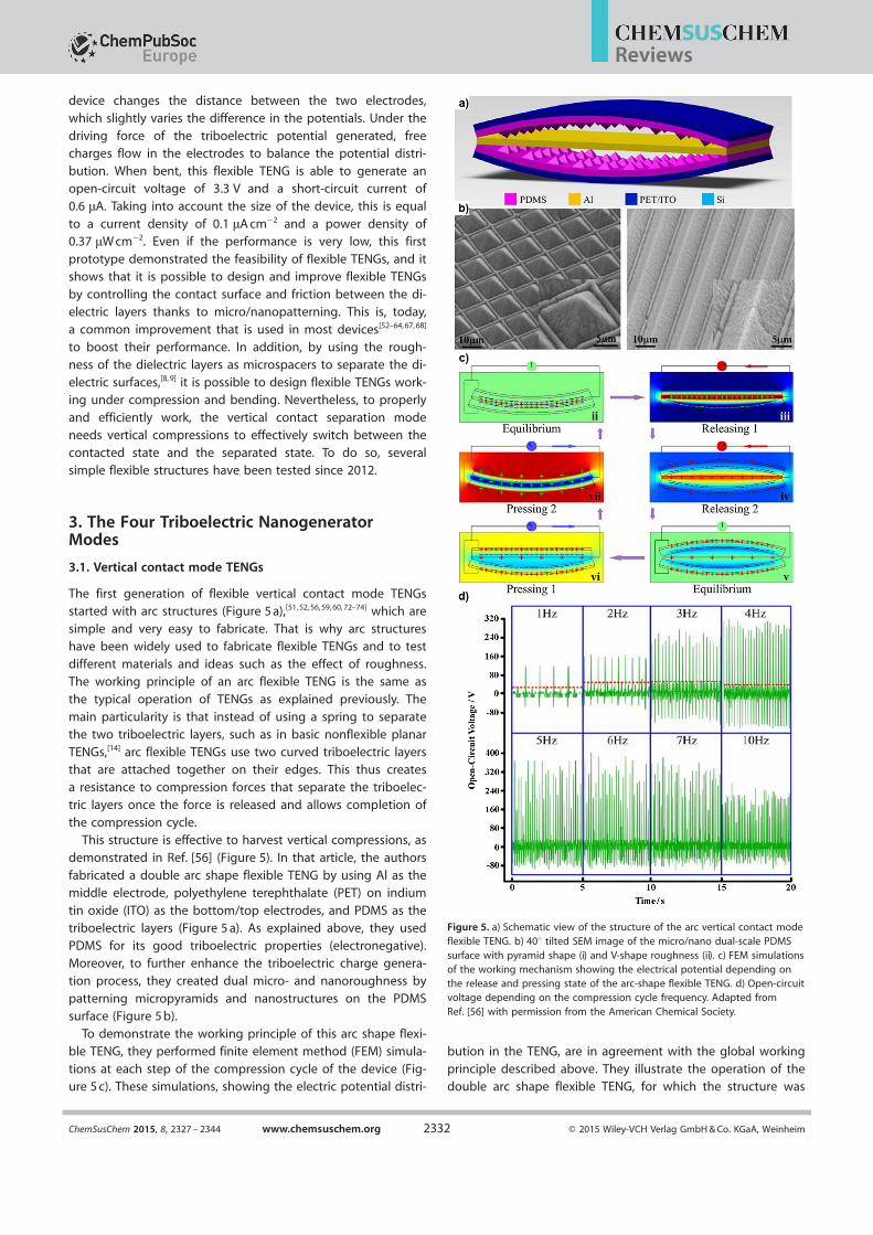
The first generation of flexible vertical contact mode TENGsstarted with arc structures (Figure 5 a),[51, 52, 56, 59, 60, 72–74] which are
simple and very easy to fabricate. That is why arc structureshave been widely used to fabricate flexible TENGs and to test
different materials and ideas such as the effect of roughness.The working principle of an arc flexible TENG is the same as
the typical operation of TENGs as explained previously. The
main particularity is that instead of using a spring to separatethe two triboelectric layers, such as in basic nonflexible planar
TENGs,[14] arc flexible TENGs use two curved triboelectric layersthat are attached together on their edges. This thus createsa resistance to compression forces that separate the triboelec-tric layers once the force is released and allows completion of
the compression cycle.This structure is effective to harvest vertical compressions, as
demonstrated in Ref. [56] (Figure 5). In that article, the authorsfabricated a double arc shape flexible TENG by using Al as themiddle electrode, polyethylene terephthalate (PET) on indium
tin oxide (ITO) as the bottom/top electrodes, and PDMS as thetriboelectric layers (Figure 5 a). As explained above, they used
PDMS for its good triboelectric properties (electronegative).Moreover, to further enhance the triboelectric charge genera-
tion process, they created dual micro- and nanoroughness by
patterning micropyramids and nanostructures on the PDMSsurface (Figure 5 b).
To demonstrate the working principle of this arc shape flexi-ble TENG, they performed finite element method (FEM) simula-
tions at each step of the compression cycle of the device (Fig-ure 5 c). These simulations, showing the electric potential distri-
bution in the TENG, are in agreement with the global working
principle described above. They illustrate the operation of thedouble arc shape flexible TENG, for which the structure was
Figure 5. a) Schematic view of the structure of the arc vertical contact modeflexible TENG. b) 408 tilted SEM image of the micro/nano dual-scale PDMSsurface with pyramid shape (i) and V-shape roughness (ii). c) FEM simulationsof the working mechanism showing the electrical potential depending onthe release and pressing state of the arc-shape flexible TENG. d) Open-circuitvoltage depending on the compression cycle frequency. Adapted fromRef. [56] with permission from the American Chemical Society.
ChemSusChem 2015, 8, 2327 – 2344 www.chemsuschem.org Ó 2015 Wiley-VCH Verlag GmbH & Co. KGaA, Weinheim2332
Reviews

optimized and compacted. Under external forces, this deviceexhibited very good performance. During characterization, the
open-circuit voltage was measured depending on the com-pression cycle frequency. As a result, the optimum stimulation
frequency found was 5 Hz (Figure 5 d). Above this value, thedevice does not have time to recover its original shape during
the release phase, which decreases its output voltage. Thisshows that the mechanical properties of the device are also
important. Overall, in its optimal configuration, this devices
generates an open-circuit voltage of 465 V and a short-circuitcurrent of 107.5 mA, corresponding to a current density of
13.4 mA cm¢2. Thus, the power density harvested reaches6.23 mW cm¢2, which is high and encouraging.
Another way to easily fabricate flexible TENGs is to useplanar structures (planar dielectric layer and electrodes) in con-
junction with elastic spacers[54, 58, 64, 65] or rigid spacers.[63, 75] They
are very similar to the structures used by nonflexible TENGsexcept that they use spacers instead of springs and flexible
layers that are bent between the spacers to allow the deviceto be flexible. These structures are interesting, because they
are simple and two dimensional. Thus, they can be adapted tolarge-scale and mass-fabrication technologies, and they can be
presented in the form of 2 D flexible layers that can be easily
rolled, transported, and installed as TENG layers.This concept has been illustrated[58] by using simple materi-
als : ITO/PET as the top electrode/triboelectric layer, foam asspacers, and PDMS/Cu as the bottom triboelectric layer/elec-
trode. Thus, it was possible to fabricate a cheap, thin, and verylarge surface of flexible TENGs, similar to a flexible TENG layer
that can be rolled and shaped at will. As an example, the au-
thors[58] cut the shape of a shoe insole and used it to generateelectrical energy in shoes while walking.
More impressive is the integration of such a planar flexibleTENG into a living rat.[54] The authors developed a planar flexi-
ble TENG (Figure 6 a, b) by using a micropatterned PDMS layer(Figure 6 c), Al foil (Figure 6 d), and flexible PET spacers (400 mmthickness). The working principle of this device is based on the
flexibility and the vertical contact–separation of the PDMS andAl layers (Figure 6 e), which enables the electrical energy to beharvested by following the same fundamental mechanism asthat previously explained. The prototype fabricated was rather
small (1.2 cm Õ 1.2 cm) to fit the specificities of rats’ in vivostructures. The PET spacers fully enclose the gap in the device
to protect the inner structure from the surrounding bioenvir-
onment. In addition, the whole device was covered by usinga thin and flexible PDMS layer (50 mm thickness) as the encap-
sulation material because of its flexibility, resistance to leaks,biocompatibility, and mild inflammatory reaction upon implan-
tation. Moreover, this polymer layer protects the device frombiofluids and increases its robustness. Because of the spacers
and all the packaging, the active surface of the device was esti-
mated to be 0.8 cm Õ 0.8 cm, which is very small for a flexibleTENG. Therefore, the performance of this device was low if
compressed; the open-circuit voltage reached 12 V and theshort-circuit current was 0.25 mA, which is equivalent to
a power density of 0.844 mW cm¢2. For realistic characterizationof the planar flexible TENG as a pacemaker in vivo energy
source, it was implanted under the thoracic skin of a rat (Fig-
ure 6 f) to serve as a breath energy harvester. The open-circuitvoltage generated by the breath of the rat was 3.73 V (Fig-
ure 6 g) and the short-circuit current was 0.14 mA (Figure 6 h).Of course, these results are inferior to those previously ob-
Figure 6. a) Structure of the implantable planar flexible TENG (iTENG).b) Photo of the iTENG. SEM image of c) the PDMS film with roughness andd) the aluminum foil. e) Working principle of the iTENG under compressioncycles. f) iTENG buried under thoracic skin. g) Short-circuit current andh) open-circuit voltage of the iTENG under stimulation of the breath ofa living rat. Adapted from Ref. [54] with permission from Wiley.
ChemSusChem 2015, 8, 2327 – 2344 www.chemsuschem.org Ó 2015 Wiley-VCH Verlag GmbH & Co. KGaA, Weinheim2333
Reviews

tained, but this voltage is sufficient to power a com-mercial pacemaker. All in all, because of the low cur-
rent, five breaths are necessary to activate a commer-cial pacemaker. However, considering the small size
of the planar flexible TENG due to the rat’s size, im-planting a larger device in the human body should
allow a commercial pacemaker to be powered ateach breath. These results are encouraging and dem-
onstrate the integration capabilities and potential ap-
plications of flexible TENGs in biology and medicine.Similar to previous planar structures, bent struc-
tures with joints or folds[67, 70, 76] have also been realiz-ed. These structures are very flexible and allow the
rotation of layers around articulations, which add onemore degree of freedom to the structures. To obtain
more degrees of freedom between the two parts of
flexible TENGs and thus to allow various integrationpossibilities, fully separated structures (two free
parts)[53, 57, 62, 66, 77] (Figure 7 a) were proposed in late2013. This structure simply consists in attaching each
triboelectric part of the flexible TENG onto differentobjects that touch each other periodically. Of course,
the two electrodes have to be electrically connected,
and every time the triboelectric layers come into con-tact with each other, electrical energy is generated.
This structure has the disadvantage to be composedof two parts, which makes it more difficult to inte-
grate, but this is also its strong point, as it allows me-chanical energy to be harvested in diverse and vari-
ous situations such as in cloths[66] or between two
pieces of clothing.[57] In this last example, the authorsconsidered a flexible TENG constituted of two fully
separated triboelectric structures : the first one wasa Cu foil covered with a microstructured PDMS tribo-
electric layer (Figure 7 a) and the second one wasa simple Al foil. If the Cu and Al are electrically con-
nected, a flexible TENG working in the contact–sepa-
ration mode is created. Indeed, upon compression, the open-circuit voltage was 83 V and the short-circuit current was
0.32 mA cm¢2. By consequence, even if this structure is verysimple, it can act as a flexible TENG if the two different parts
are attached onto two surfaces that are accustomed to touchthemselves. As a demonstration, the authors decided to inte-
grate these layers between two pieces of clothing: a shirt anda T-shirt (Figure 7 b). Thus, if the subject is walking, the shirtand T-shirt touch and slide against each other, which easily
generates a voltage up to 10 V and a current density of0.01 mA cm¢2. Naturally, the power density generated is small,
but this is an interesting concept, because we are constantlymoving with large surfaces and multiple layers of clothing
every day, and this could lead to the generation of a non-negli-
gible quantity of electrical energy over time. In addition, it hasbeen noted that more violent movements, such as clapping
the clothes together, can generate much more energy, up to100 V and 1.35 mA cm¢2.
Finally, vertical contact mode flexible TENGs have also beenadapted into tangled fibers (Figure 8)[69, 78] and then integrated
into clothes. The performance reported is not as good as thatof the other flexible TENGs previously discussed, but this appli-
cation is an interesting initiative demonstrating the integrationof flexible TENGs in clothes. To do so, the authors used cotton
thread (Figure 8 a) that they coated with carbon nanotubes(CNTs) as electrodes (Figure 8 b, c), and PTFE was used as the
triboelectric dielectric layers (Figure 8 d, e). Finally, to assemble
the device they tangled the fibers together and integratedthem into a textile to prove the concept of fiber-based flexible
TENGs. The working principle of this device is similar to that ofvertical contact mode TENGs in that the contact–separation of
a triboelectric dielectric layer with an electrode drives the elec-trons from one electrode to the other to generate current
pulses (Figure 8 i). Even if the output current of one fiber is
very low, 11.2 nA, this device can still be used as a self-pow-ered mechanical sensor. Or maybe the use of a huge number
of TENG fibers integrated in a full cloth could generate enoughpower to be considered as an interesting mechanical energy
harvesting device. Most of these flexible TENGs exhibit a highoutput voltage from a few volts to hundreds of volts, but on
Figure 7. a) Schematic of the fully separated planar structure of a flexible TENG and SEMimage of the PDMS nanostructured triboelectric layer. b) Open-circuit voltage andc) short-circuit current density of the TENG stuck onto clothes when clapping. d) Photoof the working TENG stuck on clothes. e) Snapshots of several white light-emittingdiodes connected in series before (left) and while (right) clapping the clothes. Adaptedfrom Ref. [57] with permission from Elsevier.
ChemSusChem 2015, 8, 2327 – 2344 www.chemsuschem.org Ó 2015 Wiley-VCH Verlag GmbH & Co. KGaA, Weinheim2334
Reviews

the other hand, their output current density is rather small
from a few nA cm¢2 to tens of mA cm¢2. As for piezoelectricnanogenerators, this is a disadvantage for this technology, andtherefore, research has been conducted to increase the output
current density of TENGs and flexible TENGs.TENGs use the triboelectric charges generated at the surface
of triboelectric dielectric materials to attract electrons from theoutput circuit. These electrons come back and forth in the
electrodes to screen the triboelectric charges. By consequence,the number of charges moved Q is a function of the capacity
C of the capacitor formed by the electrodes and the difference
in potential DV created by the separation of the triboelectriccharges [Eq. (2)] .[40]
Q ¼ C DV ð2Þ
With C proportional to the surface of the electrodes and in-
versely proportional to the distance between the electrodes,Equation (3) is obtained.[40]
C ¼ eair
Sd tð Þ ð3Þ
The current I generated by the TENG is by defini-tion the variation in the charge over time, which isproportional to the triboelectric charge density gen-erated s, the surface of the electrode S, and thespeed of the mechanical movement v(t), but it is in-versely proportional to the square of the distance be-
tween the electrodes [Eq. (4)] .[40]
I ¼ dQdt¼ s ¡ S ¡ d0 ¡ v tð Þ
d0 þ d tð Þ½ ¤2 ð4Þ
in which d0 is the effective thickness of the device,which is equal to [Eq. (5)]:
d0 ¼d1
e1þ d2
e2
ð5Þ
Thus, on the basis of Equation (4), there are severalparameters and approaches to increase the output
current of TENGs. First, it is possible to increase thecurrent by increasing the quantity of triboelectric
charges generated. As discussed above, triboelectric
dielectric materials should be well chosen accordingto triboelectric series. In addition, an increase in the
roughness and the friction will also increase thenumber of charges generated. This is the first ap-
proach that has been used on flexible TENGs. Anoth-er solution to increase the current would be to in-
crease the movement speed v(t) of the contact–sepa-
ration cycles, but this mainly depends on the me-chanical stimulation source, and it is difficult for verti-
cal contact mode structures to take advantage of thisparameter.
Naturally, an increase in the surface of the device will also in-
crease the output current. This can be achieved by increasingthe device size, which is easy if using a 2 D structure such as
planar TENGs with spacers.[54, 58, 63–65, 75] This problem can also be
addressed by arranging devices in parallel. This has been doneby using nonflexible TENGs in vertical contact mode,[79] but
this is not very convenient. Then, more dense designs havebeen realized by using flexible TENGs in vertical contact mode
based on arc structures[59] and folded structures.[67, 70] Resultswere better, but recently, higher performances have been ob-
tained by using a dense stack structure based on lateral slidingmode TENGs.[80] This new structure has the advantages to beflexible, easier to fabricate, and is more compact than vertical
contact mode structures. These are some strong points of lat-eral sliding mode structures but are not the only ones.
3.2. Lateral sliding mode TENGs
The structure employed by lateral sliding mode TENGs is thesame as that of vertical contact mode structures. It is constitut-
ed of one or two dielectric layers with two metal electrodes.The electric energy is also generated through periodic contact
and separation between the two triboelectric surfaces.[41, 42]
Consequently, some vertical contact mode flexible TENGs
Figure 8. a) Schematic of the fabrication process of the fiber-based TENG (FB-TENG).b) Low- and c) high-magnification SEM images of a carbon nanotube coated cottonthread. d) Low- and e) high-magnification SEM images of PTFE and carbon nanotubecoated cotton thread. f) Photo of a typical FB-TENG that is then g) bent and h) woveninto fabric. i) Power generation mechanism of a FB-TENG in the original (i), stretching (ii),and releasing (iii) states. Adapted from Ref. [69] with permission from the AmericanChemical Society.
ChemSusChem 2015, 8, 2327 – 2344 www.chemsuschem.org Ó 2015 Wiley-VCH Verlag GmbH & Co. KGaA, Weinheim2335
Reviews

having a fully separated planar structure can alsowork in the lateral sliding mode.[53, 57, 62, 77] In the lateral
sliding mode, the contact–separation of the tribo-electric surfaces takes place in a lateral sliding move-
ment parallel to the surfaces. This sliding and frictionbetween the two surfaces improves the creation of
triboelectric charges on the surfaces relative to thatin the vertical contact mode. At the same time, later-
al polarization is created along the sliding direction,
which drives the electrons in the top and bottomelectrodes to flow to balance the electric field creat-
ed by separation of the triboelectric charges. Then,the periodic back and forth sliding cycles generates
an alternating output electrical signal.Such a sliding process can be obtained by using
planar motions,[23, 81] disc rotations,[24, 25, 82, 83] or cylin-
drical rotations.[84, 85] The first devices were rigid, butthen some flexible versions were developed based
on planar motions[22, 86–88] and cylindrical rota-tions.[89, 90] In comparison to the vertical contact
mode, the lateral sliding mode offers several impor-tant advantages. The generation of the triboelectric
charges from the relative sliding and friction between
the two triboelectric surfaces is more efficient thanwith only a pure contact. Naturally, the increased fric-
tion could possibly decrease the lifetime of thedevice, but to date, there are no reports detailing
this fact. Nevertheless, to address this issue some re-searchers have used PTFE nanoparticles[22] or macro-
balls and macrorods.[88] Moreover, lateral sliding struc-
tures are generally denser than vertical contact struc-tures. Apart from the several advantages of lateral
sliding mode TENGs, this new operation mode allowsnew techniques to harvest mechanical energy from
more sources and types of movements. This improve-ment in the ability to harvest energy from various
stimuli is interesting, as it increases the mechanical
energy harvesting possibilities and the potential ap-plications in complementarity to vertical contact
mode structures.The lateral sliding mode was a great advancement
for TENGs, because it brings new advantages and in-tegration possibilities, but also because this structure
allows the development and optimization of newtechniques to improve the performance of TENGs. Indeed, it iseasier to control the movement and speed of the contact–sep-aration process by using a lateral sliding structure. For exam-ple, through making grated structures,[22, 86, 87] the lateral sensi-
tivity can be increased, the cycle speed can be multiplied, andthe lateral contact–separation process can be performed multi-
ple times in a full sliding motion, all of which result in more ef-
ficient charge transfer and a significant increase in the poweroutput. Especially, the grated structure enables multiple con-
tact–separation cycles in one full sliding motion, and this isequivalent to multiplying the speed of the contact–separation
mechanism v(t), which increases the output current density.
This improvement has been remarkably demonstrated byusing a grated structure made of metal (20 nm Ti + 500 nm Cu)grated electrodes (1 mm width) deposited on both faces ofa PTFE film (25 mm thickness) (Figure 9 a).[22] The micrograted
TENG (MG-TENG) had a surface of 60 cm2 and a weight of0.6 g. Operation of this device is similar to that of lateral sliding
mode TENGs (Figure 9 b), but it is a little bit more complex, as
the authors optimized the structure by using a double-gratedpattern to maximize the electrons exchanged between the
electrodes during one lateral translation (Figure 9 c). Duringthe relative lateral motion of the MG-TENG layers, the electrons
go back and forth between the electrodes, and this generatesa current pulse. However, because the MG-TENG is a collection
Figure 9. a) Schematic illustration of the thin film composed of a micrograted TENG (MG-TENG). The magnified illustration (bottom left) shows the structure of the MG-TENG con-sisting of a PTFE layer and a pair of metal gratings with alternating patterns (i). Photo ofa flexible MG-TENG (ii) ; because the grated pattern is alternating, the device is opaque.SEM image of PTFE nanoparticles applied on the surfaces of the MG-TENG to increase itsenergy conversion efficiency and mechanical robustness (iii). b) Basic lateral sliding modeoccurring in a MG-TENG that has a conductor–insulator–conductor structure with twoelectrodes. The contact electrode is aligned with the PTFE layer (i). The relative lateralmotion between the contact electrode and the PTFE layer decreases with overlap.During this process, the PTFE uncompensated surface triboelectric charges increases,which drives free electrons from the back electrode to the contact electrode (ii). The mis-alignment decreases as the contact electrode and the PTFE overlap, which leads toa back flow of electrons from the contact electrode to the back electrode (iii). c) First lat-eral moving cycle of the electricity generation process in a MG-TENG if both the top andbottom electrodes are connected to the base electrodes. The yellow- and green-labeledcomponents belong to the top and bottom layers, respectively. Sliding from the alignedstate (i) to the misaligned state (ii) generates a flow of electrons between the electrodes.Adapted from Ref. [22] with permission from Wiley.
ChemSusChem 2015, 8, 2327 – 2344 www.chemsuschem.org Ó 2015 Wiley-VCH Verlag GmbH & Co. KGaA, Weinheim2336
Reviews

of repeated patterns, one full relative continuous motion ofthe grated layers results in multiple microsliding cycles, which
generates multiple alternating current pulses. Thus, by usinga grated structure it is possible to multiply the number of slid-
ing cycles, and this is equivalent to increasing the lateral slid-ing speed. As a consequence, the authors were able to in-
crease the current output density and the power density gen-erated by the MG-TENG. This result is not obvious, as the total
electrode surface of a grated device is 50 % smaller than the
same non-grated device, which should decrease the current.However, this loss is compensated by an increase in the speed,
which multiplies and increases the current generated. By con-sequence, the overall effect on the output power density gen-
erated is positive. In addition, the design of the structure pro-posed was optimized (grated size compared to film thickness)to maximize the benefit offered by the grated structure.
During characterization, the fabricated MG-TENG showed im-pressive results. Stimulated by a sliding movement at a fre-
quency of 5 Hz and a speed of 10 m s¢1, the open-circuit volt-age reached 500 V and the short-circuit current reached
9.8 mA, which is equal to an output current density of0.163 mA cm¢2. By connecting the MG-TENG to a load resist-
ance of 1 MW for more realistic results, the author measured
an output power density of 50 mW cm¢2 and calculated an effi-ciency of approximately 50 %, which is very high and new for
such a TENG. These impressive results show how it is possibleto improve the performance of flexible TENGs by using an op-
timized new sliding structure and design. This demonstratesthe high performance of laterally sliding grated structures,
which are a great improvement over vertical contact mode
TENGs. Moreover, this simple, thin, and flexible new structurehas much potential in terms of integration, which should open
the path to new applications.These optimizations were not possible by using the vertical
contact mode, but the grated lateral sliding mode enablesthese optimizations to be performed to improve the current
and the overall performance of flexible TENGs. Nevertheless,
the vertical contact mode and the lateral sliding mode remainsimilar, as they can use the same structure and they distinguish
themselves only by the type of movement they use. The lateralsliding mode enables several improvements in terms of per-formance and applications, but another interesting operationmode termed the single-electrode mode, which is fully differ-ent, was reported during the same period.
3.3. Single-electrode mode TENGs
The two modes introduced above use two electrodes that aredeposited on the triboelectric moving layers, and this gener-ates triboelectric charges upon contact. Naturally, these tribo-electric materials should be chosen to maximize the number oftriboelectric charges generated. However, every material enter-ing into contact also generates a triboelectric charge at its in-terface, and the quantity depends on the properties of onematerial relative to those of the other. Especially, this is thecase of our skin and all materials that we touch and moveevery day such as our clothes and shoes. Even if the charge
generated during contact is small, it is still interesting to har-vest the mechanical energy generated by all the contact occur-
ring in our daily life environment. However, in these cases, if itis necessary to attach an electrode, it could be very difficult
and inconvenient for practical applications, for example, if oneof the triboelectric layers is our skin.
To address this problem, flexible single electrode modeTENGs were introduced in 2013[18, 44, 47] and were more deeplystudied in 2014.[19, 43, 45, 46] In this mode, only one electrode and
triboelectric layer directly interact with a moving object. Theother electrode is just a reference electrode serving asa source of electrons. It can be a large conductor or theground. If the size of the TENG is of the order of the movingobject, then the contact or separation of any object, acting asthe triboelectric layer of the single electrode mode TENG, with
the electrode would change the local electrical field distribu-tion in the device, and this will generate an electron exchangebetween the device electrode and the reference electrode to
balance the potential between them. In this mode, althoughthe induced electron transfer between the two electrodes is
not the most efficient because of the electrostatic screeningeffect between the electrodes if they are too close,[43] the tribo-
electric objects can freely move without any restriction; this is
a very big advantage and allows multiple diversified applica-tions, including daily life objects and human skin as triboelec-
tric objects.These benefits were especially studied in a few papers[46, 47]
aiming to develop and demonstrate this concept. Prototypeswere created (Figure 10 a) by using micropatterned PDMS tri-
boelectric layers (Figure 10 b) deposited onto PET substrates
and ITO electrodes. Then, copper electrodes connected to theground were used as reference electrodes. The working princi-
ple of such a device is exactly the same as that describedabove (Figure 10 c). If an object with triboelectric properties
touches the PDMS layer, it creates triboelectric charges at theinterface. If this object separates from the PDMS surface, free
charges move to the ITO electrode to balance the electrostatic
field distribution created by the triboelectric charges remainingon the PDMS surface, and this creates a current pulse. Finally, if
the active object again comes into contact with the PDMS, thePDMS triboelectric charges are compensated, and so the freecharges accumulated in the electrode flow back into the circuitto create a second opposite current pulse. This is a very simplemechanism allowing electrical energy to be harvested from
every object that comes into contact with the PDMS triboelec-tric layer. Therefore, it is possible to harvest electrical energyfrom contact of our skin, for example, our fingers (Figure 10 d).This constitutes a special case of this device that has been thesubject of a deeper study.[46] It is very interesting, as it enablesfunctionalization of our skin to harvest electrical energy, but
also, for example, for skin sensors. In addition, because of the
materials used and their thinness, the fabricated single elec-trode mode TENG was flexible and transparent (Figure 10 e),
which is also important. By consequence, these specific func-tions and properties give TENGs of this type very strong poten-
tial in terms of integration and application in our daily life en-vironment (cell phone touch-screen energy harvesters,[18] touch
ChemSusChem 2015, 8, 2327 – 2344 www.chemsuschem.org Ó 2015 Wiley-VCH Verlag GmbH & Co. KGaA, Weinheim2337
Reviews

sensors,[47] and alarms[19]). Concerning the performance of this
flexible single electrode mode TENG, the open-circuit voltageand short-circuit current were measured while tapping on the
device. Upon tapping with a bare finger, the voltage and cur-rent achieved values of 130 V and 1 mA cm¢2, respectively,
which are rather good for such a configuration. Upon tapping
with a finger covered with a polyethylene (PE) glove, theoutput performance increased by 40 %; the voltage reached
200 V and the current reached 5 mA, which is a great improve-ment. On the contrary, upon removing the PDMS layer and
using the PET substrate as the triboelectric layer, the per-formance decreased by 36 %. Altogether, this study proved the
very interesting concept of har-vesting energy from skin contact
and its rather good performance,which opens a new route for
contact energy harvesting.The single electrode mode is
a great improvement in terms ofintegration capabilities and ap-plications. However, it is not very
efficient in every case: First, a ref-erence electrode is not used,
which decreases the potential ef-fectiveness of this structure rela-tive to that of flexible TENGsthat use the two electrodes.
Second, the electrostatic screen-ing effect between the electro-des decreases the performancesif they are too close.[43] Finally, itis not adapted to every object
size and movement. Indeed, thesingle electrode mode is based
on the contact–separation of
a triboelectric object on theTENG surface, such as an open
version of the vertical contactmode or the lateral sliding
mode. However, it is not effec-tive if a smaller object laterally
moves on the TENG surface such
as a sliding or rubbing move-ment. To address this issue, the
free-standing triboelectric layermode was introduced in 2014. It
is an equivalent version of thelateral sliding mode and aims to
harvest the mechanical energy
of any object that laterallymoves on its surface.
3.4. Free-standing triboelectriclayer mode TENGs
Upon harvesting energy fromfree-moving objects, the refer-
ence electrode of single electrode TENGs can be used to gen-
erate energy in a configuration similar to that of the otherelectrode. Considering the movement of a free-standing tribo-
electric layer on two electrodes, if this layer does not fullycover these electrodes, then its lateral movement should alter-
natively cover either one of the two electrodes, which will vary
the induced potential difference between the electrodes. Then,this potential difference drives electrons to flow from one elec-
trode to the other, which creates an electrical signal. This con-figuration is termed the free-standing triboelectric layer mode.
The first prototype of a free-standing triboelectric layer modeTENG was rigid,[49] but it was then adapted to flexible TENGs.
Figure 10. a) Schematic of the single friction surface TENG (S-TENG) by using a microstructured PDMS triboelectricfriction surface with a grounded reference electrode placed beside the induction electrode. b) SEM image of themicropatterned PDMS film. c) Energy harvesting mechanism of the S-TENG if the triboelectric friction surfaceshows a tendency to attract electrons as in contact with the active object d) Equivalent circuit model of the S-TENG upon stimulation by a human finger. e) Photo of the S-TENG demonstrating high transparency and flexibili-ty. Adapted from Ref. [47] with permission from the Royal Society of Chemistry.
ChemSusChem 2015, 8, 2327 – 2344 www.chemsuschem.org Ó 2015 Wiley-VCH Verlag GmbH & Co. KGaA, Weinheim2338
Reviews

Besides, in comparison to the single electrode mode, there isno screening effect in this mode. Therefore, the efficiency of
the free-standing triboelectric layer mode is higher than thatof the single electrode mode.
The free-standing triboelectric layer mode can have twoconfigurations. In the first type, the two electrodes are vertical-
ly aligned, face to face, and the free-standing triboelectric layermoves up and down vertically between the electrodes[91] ina manner similar to that in the vertical contact mode. Follow-
ing the same principle, the vertical movement of the triboelec-tric charged layer between the electrodes induces an alternat-ing electric field. Thus, a flow of electrons appears betweenthe electrodes to balance the electric field. Despite the factthat this design can be interesting, it has been the subject ofonly one paper to date and has not yet been adapted to flexi-
ble TENGs. Concerning the second type, the two electrodes
are laterally aligned side by side and the triboelectric layeroverlaps and slides on the electrodes. Then, similar to the first
configuration, the movement of the triboelectric charged layeror object makes the electric field fluctuate between the elec-
trodes, which generates a flow of electrons between the elec-trodes. Following this principle, TENGs using sliding[49, 50] and
rotating[25] free-standing triboelectric layers have been devel-
oped. In this configuration, the triboelectric layer does notneed to maintain contact with the electrodes during sliding.
Thus, it is possible to harvest noncontact sliding movements,[25]
which can be a big advantage, because the absence of friction
between the moving parts, after the initial contact, markedlyincreases the lifetime of the TENG. As for the single electrode
mode, the free-standing triboelectric layer mode enables me-
chanical energy to be harvested from more diverse move-ments in various situations that are not accessible to the verti-
cal contact mode and the lateral sliding mode. A few flexiblefree-standing triboelectric type TENGs have already been re-
ported. They aim to harvest different sources of mechanicalenergy by using rotations[89] and also, more interesting, for ex-
ample, random movements coming from clothes
(Figure 11)[78, 92] or liquid waves.[93, 94]
Indeed, the development of flexible TENGs integrated into
clothes is a very attractive concept, because it would enablethe generation of electric energy from large surfaces that we
carry daily with us and activate constantly, every day, every-where. In one paper,[92] the concept of the free-standing tribo-
electric layer mode was used to create triboelectric wovenstructures and, therefore, a textile-based flexible TENG namedW-TENG (Figure 11 a). This structure is composed of two tribo-
electric dielectric materials (nylon and polyester) and silverelectrodes cut into large strips, 7 mm Õ 29 cm and 5 mm Õ
27 cm. Then, the silver electrodes are pasted between twonylon or polyester strips by using acrylic adhesive to create the
final nylon and polyester strips integrating the silver electro-
des. Finally, the stripes are woven together following an alter-nating pattern to create the W-TENG. This structure is a new,
innovative, and efficient way to easily integrate flexible TENGsinto clothes. The working principle of this device is simple. If
any triboelectric layer touches (Figure 11 b) or slides on thiswoven structure, the nylon and polyester strips will have oppo-
site or different triboelectric behavior, and this induces oppo-site or different quantities of triboelectric charges at the inter-
faces with the touching triboelectric layer or object. If the free-standing triboelectric layer leaves the W-TENG, free charges
flow through the device to balance the induced potential inthe electrodes, and this creates a current pulse (Figure 11 c). If
the free-standing triboelectric layer again comes into contactwith the W-TENG, the free charges flow back to create
a second opposite current pulse. To characterize W-TENG, the
authors touched the W-TENG by using an acrylic plate with dif-ferent pressures and speeds. Under this stimulation, the W-
TENG generated a maximal open-circuit voltage of 95 V (Fig-ure 11 d) and a maximum short-circuit current of 2.5 mA (Fig-
ure 11 e), which is encouraging for this new structure. Further-more, this structure also works if the free-standing triboelectric
layer slides from one electrode to the other. In this case, it gen-
erates an electrical signal similar to that generated by two cou-pled lateral sliding mode TENGs. Thus, it is possible to harvest
energy from any sliding object but also from liquid waves os-cillating between the electrodes.[93, 94] These possibilities
expand the potential applications of free-standing triboelectriclayer mode TENGSs. It is interesting to note that recently
a rigid TENG having a free-standing triboelectric layer structure
and operating similarly to a lateral sliding grated structure[50]
succeeded in reaching an estimated energy conversion effi-
ciency of 85 %, which is, if confirmed, outstanding and demon-strates the strong potential of this mode.
4. Towards New Integrations and Applications
Since the first demonstration of TENGs, the structure anddesign of TENGs has evolved toward two complementary
goals. First, increasing the output current density, outputpower, and efficiency. Second, better integration to harvest the
mechanical energy from more diverse energy sources and
movements, thus, to develop new applications. To addressthese issues, research was focused on new structures and new
operation modes, and this resulted in the development of fouroperation modes: the vertical contact mode, the lateral sliding
mode, the single electrode mode, and the free-standing tribo-electric layer mode. It is possible to achieve great improve-
ments in terms of output power and efficiency.[22] More impor-tantly, it is now possible to harvest the mechanical energy
from many different movements present in our daily life. In ad-dition, the integration of TENGs has been enhanced, and it isnow possible to adapt the design of TENGs to many cases andsituations. Naturally, this was possible thanks to the develop-ment of flexible TENGs, but nowadays, the flexibility of TENGsis not the only wanted property. Indeed, to harvest energyfrom our daily life movements and from the environment, flexi-
ble TENGs able to harvest energy from the motion ofclothes[57, 66, 69, 92] and skin contact[18, 19, 45–47] has receive growinginterest. In addition, for better and wide integration of TENGs,
transparent flexible TENGs[9, 18, 47, 63, 65, 75] have recently receivedspecial emphasis. Needless to say, hybrid energy harvesting
and energy conversion have attracted the interest of research-ers, and flexible TENGs as a new and efficient way to harvest
ChemSusChem 2015, 8, 2327 – 2344 www.chemsuschem.org Ó 2015 Wiley-VCH Verlag GmbH & Co. KGaA, Weinheim2339
Reviews

mechanical energy are now under consideration. However, todate they have been the subject of very few developments
until now.[51, 64, 95–97] To addressthese recent concerns of trans-
parency and higher outputpower, new and innovative
structures, designs, and materialsare under investigation. Thus,
we recently explored new ultra-thin transparent electrodes
made of graphene to create
thin, flexible, robust, and trans-parent TENGs. We also studied
the use of new thin triboelectricsponge layers to create thin,
flexible, robust, and more effi-cient TENGs.
An example of a new struc-
ture is the 3 D patterning of Alelectrodes[70] and the triboelec-
tric PDMS layer;[74] this was ach-ieved to further enhance the
generation of triboelectriccharge density and the output
performance of flexible TENGs.
To proceed, the authors first de-posited a polystyrene micro-
spheres layer on a SiO2/Si sub-strate. Then, after depositing
PDMS between the micro-spheres, they etched the poly-
styrene spheres and transferred
the PDMS sponge layer obtainedon an Al electrode (Figure 12 a).
Relative to that of an equivalentPDMS thin film, the PDMS
sponge layer fabricated hada young modulus that was 30 %
smaller and much more flexible.
Moreover, the 3 D spherical pat-tern markedly increases the con-
tact area, and under the samemechanical stress, the com-
pressed sponge layer is thinnerthan the equivalent PDMS film,which makes the capacitance of
the compressed sponge layerbigger because of the higher e/d
ratio. Characterization of PDMSfilm based TENGs and PDMSsponge layer based TENGs (S-TENG) under compression cycles(90 N at 10 Hz) showed that the
open-circuit voltage (Figure 12 b)and the short-circuit current (Fig-ure 12 c) of the S-TENG reachedvalues of 130 V and
0.10 mA cm¢2 respectively, both of which are higher than thevalues shown by the film-based TENG, which achieved only
Figure 11. a) Schematic of the structure and fabrication of the textile-based free-standing triboelectric-layer modeTENG termed woven TENG (W-TENG). b) Structure of the W-TENG under vertical contact mode, for which acrylic isused as the free-standing triboelectric layer. c) Working principle of the W-TENG. d) Short-circuit current ande) open-circuit voltage of the W-TENG under mechanical contact with acrylic. Adapted from Ref. [92] with permis-sion from the American Chemical Society.
ChemSusChem 2015, 8, 2327 – 2344 www.chemsuschem.org Ó 2015 Wiley-VCH Verlag GmbH & Co. KGaA, Weinheim2340
Reviews

50 V and 0.02 mA cm¢2. As a result, if used as a triboelectriclayer in a TENG, the sponge PDMS layer is more efficient thanan equivalent PDMS film. In addition, the PDMS sponge layer isthinner and has a higher output voltage (Figure 12 d), and
these parameters are important to create thinner TENGs. Atthe same time, ecological, abundant, and cheap materials,
such as paper,[98] have been studied as substrates for TENGs,but new materials are also under scrutiny. For example, recent-ly, the use of 2 D materials such as hexagonal boron nitride
was studied as a triboelectric layer[99] and graphene was stud-ied as an electrode.[75, 100] For the latter, electrodes were usually
metal layers or foils. Then, ITO was used because of its trans-parency and flexibility. Recently, however, a flexible TENG with
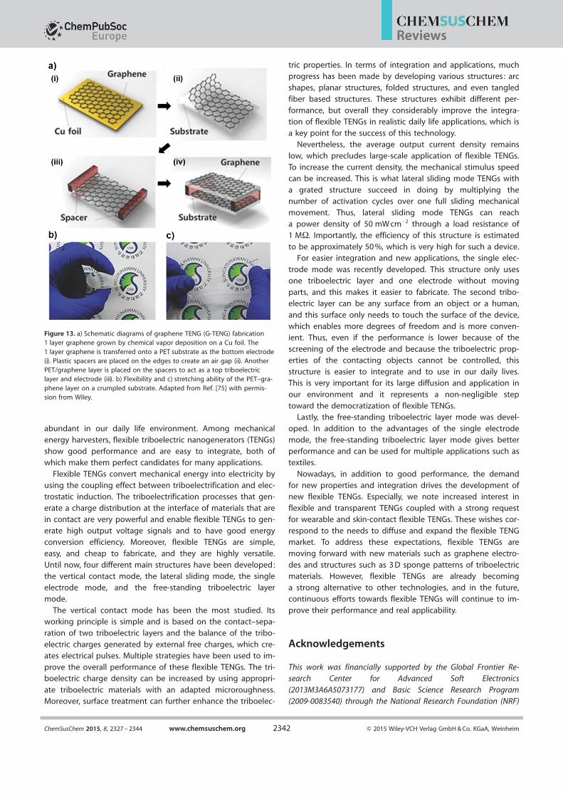
a graphene electrode was demonstrated.[75] For fabrication of
this device, a graphene monolayer grown by chemical vapordeposition on a Cu foil was used (Figure 13 a). Then, the gra-
phene monolayer sheet was transferred onto a flexible PETsubstrate to act as the bottom electrode. Spacers were depos-
ited on the edges, and to complete the device, another PET/graphene layer was added on the top to serve as an active tri-
boelectric dielectric layer/topelectrode. The fabricated device
was very thin, flexible, robust,and transparent (Figure 13 b, c).
Characterization of the graphenemonolayer TENG under a com-pressive force of 1 kg f generatedan open-circuit voltage of 5 Vand a short-circuit current densi-
ty of 0.5 mA cm¢2. Upon usinga multilayer graphene electrode,the performance reached 9 Vand 1.2 mA cm¢2, which is better
but still low relative to that ofconventional flexible TENGs.
Nevertheless, these devices were
not optimized, and the effect ofthe graphene electrode is not
yet clearly understood. Indeed,this extremely thin electrode
with special properties has dif-ferent behavior than electrodes
usually composed of deposited
metals. However, taking into ac-count the very interesting me-
chanical and electrical propertiesof graphene and the integration
capabilities that it offers, thisgives hopes for future great im-
provements in the performance
and integration of flexibleTENGs.
Overall, flexible TENGs alreadyexhibit interesting performance
and are still being improved forhigher efficiency and better inte-
gration. However, in the actual
context of energy harvesters, for which harvesting green andrenewable energy should be done with small devices that are
as ecological and as cheap as possible, the next big challengewill probably be to democratize this technology. Therefore, inthe future, progress will need to be done toward the mass fab-rication and the large-scale diffusion of flexible TENGs.
5. Summary and Conclusions
Over the last few years, autonomous smart systems have metwith large success. Especially, their importance was empha-
sized by electronic systems becoming more personal, portable,complex, multifunctional, and smart. In addition, enabling sys-
tems to work wirelessly, sustainably, and independently is
highly desirable. Thus, autonomous smart systems are adopt-ing increasingly more important roles in our daily life. Despite
all the progress in decreasing power consumption, smart sys-tems consume a great amount of energy. As a result, there is
a growing need for energy harvesters. For this purpose, har-vesting mechanical energy is essential, as it is widespread and
Figure 12. a) Structure of a sponge-based TENG (S-TENG) with SEM images of the sponge-structured PDMS film.b) Open-circuit voltage and c) short-circuit current density of a 0.5 mm thick film-based TENG and S-TENG d) Varia-tion of the output voltage of the film-based TENG and S-TENG having different thicknesses (0.5, 1, 3, and 10 mm)and depending on the magnitude of applied force ranging from 30 to 90 N. Adapted from Ref. [55] with permis-sion from Wiley.
ChemSusChem 2015, 8, 2327 – 2344 www.chemsuschem.org Ó 2015 Wiley-VCH Verlag GmbH & Co. KGaA, Weinheim2341
Reviews
abundant in our daily life environment. Among mechanicalenergy harvesters, flexible triboelectric nanogenerators (TENGs)
show good performance and are easy to integrate, both ofwhich make them perfect candidates for many applications.
Flexible TENGs convert mechanical energy into electricity by
using the coupling effect between triboelectrification and elec-trostatic induction. The triboelectrification processes that gen-erate a charge distribution at the interface of materials that arein contact are very powerful and enable flexible TENGs to gen-
erate high output voltage signals and to have good energyconversion efficiency. Moreover, flexible TENGs are simple,
easy, and cheap to fabricate, and they are highly versatile.Until now, four different main structures have been developed:the vertical contact mode, the lateral sliding mode, the single
electrode mode, and the free-standing triboelectric layermode.
The vertical contact mode has been the most studied. Itsworking principle is simple and is based on the contact–sepa-
ration of two triboelectric layers and the balance of the tribo-
electric charges generated by external free charges, which cre-ates electrical pulses. Multiple strategies have been used to im-
prove the overall performance of these flexible TENGs. The tri-boelectric charge density can be increased by using appropri-
ate triboelectric materials with an adapted microroughness.Moreover, surface treatment can further enhance the triboelec-
tric properties. In terms of integration and applications, muchprogress has been made by developing various structures : arc
shapes, planar structures, folded structures, and even tangledfiber based structures. These structures exhibit different per-
formance, but overall they considerably improve the integra-tion of flexible TENGs in realistic daily life applications, which is
a key point for the success of this technology.Nevertheless, the average output current density remains
low, which precludes large-scale application of flexible TENGs.
To increase the current density, the mechanical stimulus speedcan be increased. This is what lateral sliding mode TENGs with
a grated structure succeed in doing by multiplying thenumber of activation cycles over one full sliding mechanical
movement. Thus, lateral sliding mode TENGs can reacha power density of 50 mW cm¢2 through a load resistance of
1 MW. Importantly, the efficiency of this structure is estimated
to be approximately 50 %, which is very high for such a device.For easier integration and new applications, the single elec-
trode mode was recently developed. This structure only usesone triboelectric layer and one electrode without moving
parts, and this makes it easier to fabricate. The second tribo-electric layer can be any surface from an object or a human,
and this surface only needs to touch the surface of the device,
which enables more degrees of freedom and is more conven-ient. Thus, even if the performance is lower because of the
screening of the electrode and because the triboelectric prop-erties of the contacting objects cannot be controlled, this
structure is easier to integrate and to use in our daily lives.This is very important for its large diffusion and application in
our environment and it represents a non-negligible step
toward the democratization of flexible TENGs.Lastly, the free-standing triboelectric layer mode was devel-
oped. In addition to the advantages of the single electrodemode, the free-standing triboelectric layer mode gives better
performance and can be used for multiple applications such astextiles.
Nowadays, in addition to good performance, the demand
for new properties and integration drives the development ofnew flexible TENGs. Especially, we note increased interest in
flexible and transparent TENGs coupled with a strong requestfor wearable and skin-contact flexible TENGs. These wishes cor-respond to the needs to diffuse and expand the flexible TENGmarket. To address these expectations, flexible TENGs aremoving forward with new materials such as graphene electro-
des and structures such as 3 D sponge patterns of triboelectricmaterials. However, flexible TENGs are already becoming
a strong alternative to other technologies, and in the future,continuous efforts towards flexible TENGs will continue to im-prove their performance and real applicability.
Acknowledgements
This work was financially supported by the Global Frontier Re-search Center for Advanced Soft Electronics
(2013M3A6A5073177) and Basic Science Research Program(2009-0083540) through the National Research Foundation (NRF)
Figure 13. a) Schematic diagrams of graphene TENG (G-TENG) fabrication1 layer graphene grown by chemical vapor deposition on a Cu foil. The1 layer graphene is transferred onto a PET substrate as the bottom electrode(i). Plastic spacers are placed on the edges to create an air gap (ii). AnotherPET/graphene layer is placed on the spacers to act as a top triboelectriclayer and electrode (iii). b) Flexibility and c) stretching ability of the PET–gra-phene layer on a crumpled substrate. Adapted from Ref. [75] with permis-sion from Wiley.
ChemSusChem 2015, 8, 2327 – 2344 www.chemsuschem.org Ó 2015 Wiley-VCH Verlag GmbH & Co. KGaA, Weinheim2342
Reviews

of Korea funded by the Ministry of Science, ICT & Future Plan-ning.
Keywords: energy conversion · energy harvesting ·nanogenerators · nanostructures · triboelectric charging
[1] A. Nathan, A. Ahnood, M. T. Cole, Y. Suzuki, P. Hiralal, F. Bonaccorso, T.Hasan, L. Garcia-Gancedo, A. Dyadyusha, S. Haque, P. Andrew, S. Hof-mann, J. Moultrie, A. J. Flewitt, A. C. Ferrari, M. J. Kelly, J. Robertson,G. A. J. Amaratunga, W. I. Milne, Proc. IEEE 2012, 100, 1486 – 1517.
[2] Flexible Electronics, 11 (Eds. : W. S. Wong, A. Salleo), Springer, Boston,MA, 2009.
[3] Z. L. Wang, Sci. Am. 2008, 298, 82 – 87.[4] Z. L. Wang, Adv. Mater. 2012, 24, 280 – 285.[5] Z. L. Wang, W. Wu, Angew. Chem. Int. Ed. 2012, 51, 11700 – 11721;
Angew. Chem. 2012, 124, 11868 – 11891.[6] Z. L. Wang, J. Song, Science 2006, 312, 242 – 246.[7] Z. L. Wang, G. Zhu, Y. Yang, S. Wang, C. Pan, Mater. Today 2012, 15,
532 – 543.[8] F.-R. Fan, Z.-Q. Tian, Z. L. Wang, Nano Energy 2012, 1, 328 – 334.[9] F.-R. Fan, L. Lin, G. Zhu, W. Wu, R. Zhang, Z. L. Wang, Nano Lett. 2012,
12, 3109 – 3114.[10] G. S. P. Castle, J. Electrost. 1997, 40 – 41, 13 – 20.[11] A. F. Diaz, R. M. Felix-Navarro, J. Electrost. 2004, 62, 277 – 290.[12] L. S. McCarty, G. M. Whitesides, Angew. Chem. Int. Ed. 2008, 47, 2188 –
2207; Angew. Chem. 2008, 120, 2218 – 2239.[13] H. T. Baytekin, A. Z. Patashinski, M. Branicki, B. Baytekin, S. Soh, B. A.
Grzybowski, Science 2011, 333, 308 – 312.[14] Z. L. Wang, ACS Nano 2013, 7, 9533 – 9557.[15] Z. L. Wang, Faraday Discuss. 2014, 176, 447 – 458.[16] S. Wang, L. Lin, Z. L. Wang, Nano Energy 2015, 11, 436 – 462.[17] X.-S. Zhang, M.-D. Han, B. Meng, H.-X. Zhang, Nano Energy 2015, 11,
304 – 322.[18] Y. Yang, H. Zhang, Z.-H. Lin, Y. S. Zhou, Q. Jing, Y. Su, J. Yang, J. Chen,
C. Hu, Z. L. Wang, ACS Nano 2013, 7, 9213 – 9222.[19] G. Zhu, W. Q. Yang, T. Zhang, Q. Jing, J. Chen, Y. S. Zhou, P. Bai, Z. L.
Wang, Nano Lett. 2014, 14, 3208 – 3213.[20] G. Zhu, Z.-H. Lin, Q. Jing, P. Bai, C. Pan, Y. Yang, Y. Zhou, Z. L. Wang,
Nano Lett. 2013, 13, 847 – 853.[21] L. Lin, Y. Xie, S. Wang, W. Wu, S. Niu, X. Wen, Z. L. Wang, ACS Nano
2013, 7, 8266 – 8274.[22] G. Zhu, Y. S. Zhou, P. Bai, X. S. Meng, Q. Jing, J. Chen, Z. L. Wang, Adv.
Mater. 2014, 26, 3788 – 3796.[23] S. Wang, L. Lin, Y. Xie, Q. Jing, S. Niu, Z. L. Wang, Nano Lett. 2013, 13,
2226 – 2233.[24] L. Lin, S. Wang, Y. Xie, Q. Jing, S. Niu, Y. Hu, Z. L. Wang, Nano Lett.
2013, 13, 2916 – 2923.[25] L. Lin, S. Wang, S. Niu, C. Liu, Y. Xie, Z. L. Wang, ACS Appl. Mater. Interfa-
ces 2014, 6, 3031 – 3038.[26] J. Chen, G. Zhu, W. Yang, Q. Jing, P. Bai, Y. Yang, T.-C. Hou, Z. L. Wang,
Adv. Mater. 2013, 25, 6094 – 6099.[27] J. Yang, J. Chen, Y. Liu, W. Yang, Y. Su, Z. L. Wang, ACS Nano 2014, 8,
2649 – 2657.[28] Y. H. Do, W. S. Jung, M. G. Kang, C. Y. Kang, S. J. Yoon, Sens. Actuators A
2013, 200, 51 – 55.[29] S. Lee, S.-H. Bae, L. Lin, Y. Yang, C. Park, S.-W. Kim, S. N. Cha, H. Kim,
Y. J. Park, Z. L. Wang, Adv. Funct. Mater. 2013, 23, 2445 – 2449.[30] K.-I. Park, S. Xu, Y. Liu, G.-T. Hwang, S.-J. L. Kang, Z. L. Wang, K. J. Lee,
Nano Lett. 2010, 10, 4939 – 4943.[31] L. Lin, Y. Hu, C. Xu, Y. Zhang, R. Zhang, X. Wen, Z. L. Wang, Nano
Energy 2013, 2, 75 – 81.[32] Z.-H. Lin, Y. Yang, J. M. Wu, Y. Liu, F. Zhang, Z. L. Wang, J. Phys. Chem.
Lett. 2012, 3, 3599 – 3604.[33] S. Xu, Y. Qin, C. Xu, Y. Wei, R. Yang, Z. L. Wang, Nat. Nanotechnol. 2010,
5, 366 – 373.[34] Y. Qi, M. C. McAlpine, Energy Environ. Sci. 2010, 3, 1275.[35] J. A. Wiles, B. A. Grzybowski, A. Winkleman, G. M. Whitesides, Anal.
Chem. 2003, 75, 4859 – 4867.[36] D. K. Davies, J. Phys. D 1969, 2, 1533 – 1537.
[37] J. Henniker, Nature 1962, 196, 474 – 474.[38] S. Boisseau, G. Despesse, A. Sylvestre, Smart Mater. Struct. 2010, 19,
075015.[39] Y. Suzuki, IEEJ Trans. Electr. Electron. Eng. 2011, 6, 101 – 111.[40] S. Niu, S. Wang, L. Lin, Y. Liu, Y. S. Zhou, Y. Hu, Z. L. Wang, Energy Envi-
ron. Sci. 2013, 6, 3576.[41] S. Niu, Y. Liu, S. Wang, L. Lin, Y. S. Zhou, Y. Hu, Z. L. Wang, Adv. Mater.
2013, 25, 6184 – 6193.[42] S. Niu, S. Wang, Y. Liu, Y. S. Zhou, L. Lin, Y. Hu, K. C. Pradel, Z. L. Wang,
Energy Environ. Sci. 2014, 7, 2339.[43] S. Niu, Y. Liu, S. Wang, L. Lin, Y. S. Zhou, Y. Hu, Z. L. Wang, Adv. Funct.
Mater. 2014, 24, 3332 – 3340.[44] Y. Yang, H. Zhang, J. Chen, Q. Jing, Y. S. Zhou, X. Wen, Z. L. Wang, ACS
Nano 2013, 7, 7342 – 7351.[45] W. Yang, J. Chen, X. Wen, Q. Jing, J. Yang, Y. Su, G. Zhu, W. Wu, Z. L.
Wang, ACS Appl. Mater. Interfaces 2014, 6, 7479 – 7484.[46] B. Meng, X. Cheng, X. Zhang, M. Han, W. Liu, H. Zhang, Appl. Phys. Lett.
2014, 104, 103904.[47] B. Meng, W. Tang, Z. Too, X. Zhang, M. Han, W. Liu, H. Zhang, Energy
Environ. Sci. 2013, 6, 3235.[48] S. Niu, Y. Liu, X. Chen, S. Wang, Y. S. Zhou, L. Lin, Y. Xie, Z. Lin, Nano
Energy 2015, 12, 760 – 774.[49] S. Wang, Y. Xie, S. Niu, L. Lin, Z. L. Wang, Adv. Mater. 2014, 26, 2818 –
2824.[50] Y. Xie, S. Wang, S. Niu, L. Lin, Q. Jing, J. Yang, Z. Wu, Z. L. Wang, Adv.
Mater. 2014, 26, 6599 – 6607.[51] Y. Yang, H. Zhang, J. Chen, S. Lee, T.-C. Hou, Z. L. Wang, Energy Environ.
Sci. 2013, 6, 1744.[52] S. Wang, L. Lin, Z. L. Wang, Nano Lett. 2012, 12, 6339 – 6346.[53] S. Lee, Y. Lee, D. Kim, Y. Yang, L. Lin, Z.-H. Lin, W. Hwang, Z. L. Wang,
Nano Energy 2013, 2, 1113 – 1120.[54] Q. Zheng, B. Shi, F. Fan, X. Wang, L. Yan, W. Yuan, S. Wang, H. Liu, Z. Li,
Z. L. Wang, Adv. Mater. 2014, 26, 5851 – 5856.[55] K. Y. Lee, J. Chun, J.-H. Lee, K. N. Kim, N.-R. Kang, J.-Y. Kim, M. H. Kim,
K.-S. Shin, M. K. Gupta, J. M. Baik, S.-W. Kim, Adv. Mater. 2014, 26,5037 – 5042.
[56] X.-S. Zhang, M.-D. Han, R.-X. Wang, F.-Y. Zhu, Z.-H. Li, W. Wang, H.-X.Zhang, Nano Lett. 2013, 13, 1168 – 1172.
[57] H. Zhang, Y. Yang, T.-C. Hou, Y. Su, C. Hu, Z. L. Wang, Nano Energy2013, 2, 1019 – 1024.
[58] T.-C. Hou, Y. Yang, H. Zhang, J. Chen, L.-J. Chen, Z. L. Wang, NanoEnergy 2013, 2, 856 – 862.
[59] W. Tang, B. Meng, H. X. Zhang, Nano Energy 2013, 2, 1164 – 1171.[60] X.-S. Zhang, M.-D. Han, R.-X. Wang, B. Meng, F.-Y. Zhu, X.-M. Sun, W.
Hu, W. Wang, Z.-H. Li, H.-X. Zhang, Nano Energy 2014, 4, 123 – 131.[61] Y. H. Ko, N. Goli, J. S. Yu, RSC Adv. 2015, 5, 6437 – 6442.[62] Z.-H. Lin, G. Cheng, L. Lin, S. Lee, Z. L. Wang, Angew. Chem. Int. Ed.
2013, 52, 12545 – 12549; Angew. Chem. 2013, 125, 12777 – 12781.[63] Y. H. Ko, S. H. Lee, J. W. Leem, J. S. Yu, RSC Adv. 2014, 4, 10216.[64] M. Han, X.-S. Zhang, B. Meng, W. Liu, W. Tang, X. Sun, W. Wang, H.
Zhang, ACS Nano 2013, 7, 8554 – 8560.[65] F. R. Fan, J. Luo, W. Tang, C. Li, C. Zhang, Z. Tian, Z. L. Wang, J. Mater.
Chem. A 2014, 2, 13219 – 13225.[66] W. Seung, M. K. Gupta, K. Y. Lee, K.-S. Shin, J.-H. Lee, T. Y. Kim, S. Kim, J.
Lin, J. H. Kim, S.-W. Kim, ACS Nano 2015, 9, 3501 – 3509.[67] W. Yang, J. Chen, G. Zhu, J. Yang, P. Bai, Y. Su, Q. Jing, X. Cao, Z. L.
Wang, ACS Nano 2013, 7, 11317 – 11324.[68] C. K. Jeong, K. M. Baek, S. Niu, T. W. Nam, Y. H. Hur, D. Y. Park, G.-T.
Hwang, M. Byun, Z. L. Wang, Y. S. Jung, K. J. Lee, Nano Lett. 2014, 14,7031 – 7038.
[69] J. Zhong, Y. Zhang, Q. Zhong, Q. Hu, B. Hu, Z. L. Wang, J. Zhou, ACSNano 2014, 8, 6273 – 6280.
[70] G. Zhu, P. Bai, J. Chen, Z. L. Wang, Nano Energy 2013, 2, 688 – 692.[71] S. Wang, Y. Xie, S. Niu, L. Lin, C. Liu, Y. S. Zhou, Z. L. Wang, Adv. Mater.
2014, 26, 6720 – 6728.[72] S. Wang, Z.-H. Lin, S. Niu, L. Lin, Y. Xie, K. C. Pradel, Z. L. Wang, ACS
Nano 2013, 7, 11263 – 11271.[73] W. Tang, T. Zhou, C. Zhang, F. R. Fan, C. B. Han, Z. L. Wang, Nanotech-
nology 2014, 25, 225402.[74] Y. Zheng, L. Cheng, M. Yuan, Z. Wang, L. Zhang, Y. Qin, T. Jing, Nano-
scale 2014, 6, 7842 – 7846.
ChemSusChem 2015, 8, 2327 – 2344 www.chemsuschem.org Ó 2015 Wiley-VCH Verlag GmbH & Co. KGaA, Weinheim2343
Reviews

[75] S. Kim, M. K. Gupta, K. Y. Lee, A. Sohn, T. Y. Kim, K.-S. Shin, D. Kim, S. K.Kim, K. H. Lee, H.-J. Shin, D.-W. Kim, S.-W. Kim, Adv. Mater. 2014, 26,3918 – 3925.
[76] B. Meng, W. Tang, X. Zhang, M. Han, W. Liu, H. Zhang, Nano Energy2013, 2, 1101 – 1106.
[77] L. Zhang, F. Xue, W. Du, C. Han, C. Zhang, Z. Wang, Nano Res. 2014, 7,1215 – 1223.
[78] X. Pu, L. Li, H. Song, C. Du, Z. Zhao, C. Jiang, G. Cao, W. Hu, Z. L. Wang,Adv. Mater. 2015, 27, 2472 – 2478.
[79] W. Yang, J. Chen, Q. Jing, J. Yang, X. Wen, Y. Su, G. Zhu, P. Bai, Z. L.Wang, Adv. Funct. Mater. 2014, 24, 4090 – 4096.
[80] W. Du, X. Han, L. Lin, M. Chen, X. Li, C. Pan, Z. L. Wang, Adv. EnergyMater. 2014, 4, 1301592.
[81] G. Zhu, J. Chen, Y. Liu, P. Bai, Y. S. Zhou, Q. Jing, C. Pan, Z. L. Wang,Nano Lett. 2013, 13, 2282 – 2289.
[82] W. Tang, C. Zhang, C. B. Han, Z. L. Wang, Adv. Funct. Mater. 2014, 24,6684 – 6690.
[83] Y. Xie, S. Wang, S. Niu, L. Lin, Q. Jing, Y. Su, Z. Wu, Z. L. Wang, NanoEnergy 2014, 6, 129 – 136.
[84] P. Bai, G. Zhu, Y. Liu, J. Chen, Q. Jing, W. Yang, J. Ma, G. Zhang, Z. L.Wang, ACS Nano 2013, 7, 6361 – 6366.
[85] Q. Jing, G. Zhu, W. Wu, P. Bai, Y. Xie, R. P. S. Han, Z. L. Wang, NanoEnergy 2014, 10, 305 – 312.
[86] S. Jung, J. Lee, T. Hyeon, M. Lee, D.-H. Kim, Adv. Mater. 2014, 26, 6329 –6334.
[87] W. Liu, M. Han, X. Sun, B. Meng, X.-S. Zhang, H. Zhang, Nano Energy2014, 9, 401 – 407.
[88] L. Lin, Y. Xie, S. Niu, S. Wang, P.-K. Yang, Z. L. Wang, ACS Nano 2015, 9,922 – 930.
[89] Q. Leng, H. Guo, X. He, G. Liu, Y. Kang, C. Hu, Y. Xi, J. Mater. Chem. A2014, 2, 19427 – 19434.
[90] Q. Jing, G. Zhu, P. Bai, Y. Xie, J. Chen, R. P. S. Han, Z. L. Wang, ACS Nano2014, 8, 3836 – 3842.
[91] S. Wang, S. Niu, J. Yang, L. Lin, Z. L. Wang, ACS Nano 2014, 8, 12004 –12013.
[92] T. Zhou, C. Zhang, C. B. Han, F. R. Fan, W. Tang, Z. L. Wang, ACS Appl.Mater. Interfaces 2014, 6, 14695 – 14701.
[93] Y. Su, X. Wen, G. Zhu, J. Yang, J. Chen, P. Bai, Z. Wu, Y. Jiang, Z. L.Wang, Nano Energy 2014, 9, 186 – 195.
[94] G. Zhu, Y. Su, P. Bai, J. Chen, Q. Jing, W. Yang, Z. L. Wang, ACS Nano2014, 8, 6031 – 6037.
[95] Y. Yang, H. Zhang, Y. Liu, Z.-H. Lin, S. Lee, Z. Lin, C. P. Wong, Z. L. Wang,ACS Nano 2013, 7, 2808 – 2813.
[96] Y. Hu, J. Yang, S. Niu, W. Wu, Z. L. Wang, ACS Nano 2014, 8, 7442 –7450.
[97] K. Zhang, X. Wang, Y. Yang, Z. L. Wang, ACS Nano 2015, 9, 3521 – 3529.[98] P.-K. Yang, Z.-H. Lin, K. C. Pradel, L. Lin, X. Li, X. Wen, J.-H. He, Z. L.
Wang, ACS Nano 2015, 9, 901 – 907.[99] R. Que, Y. Huang, Q. Li, H. Yao, B. Geng, M. Shao, ACS Appl. Mater. Inter-
faces 2014, 6, 19752 – 19757.[100] S. A. Han, K. H. Lee, T.-H. Kim, W. Seung, S. K. Lee, S. Choi, B. Kumar, R.
Bhatia, H.-J. Shin, W.-J. Lee, S. Kim, H. S. Kim, J.-Y. Choi, S.-W. Kim, NanoEnergy 2015, 12, 556 – 566.
Received: December 30, 2014
Published online on July 6, 2015
ChemSusChem 2015, 8, 2327 – 2344 www.chemsuschem.org Ó 2015 Wiley-VCH Verlag GmbH & Co. KGaA, Weinheim2344
Reviews