Embed Size (px)
Citation preview
Recent Progress in Vacuum-Deposited Small Molecule
Organic Solar Cells
By: Graeme Williams*
*Organic Optoelectronic Materials & Devices Laboratory, [email protected]
Electrical and Computer Engineering
University of Waterloo. Waterloo, ON Canada. N2L 3G1.
Abstract.
While solution-coated organic solar cells (OSCs) have been a strong area of research for the
past decade, recent advances in the photovoltaics industry have suggested that vacuum-
deposited small molecule OSCs may yet have a promising future in organic photovoltaics. With
vacuum-deposited devices, researchers can remove many experimental variables that are
specific to solution processing, and instead focus on understanding and optimizing the device
physics. Furthermore, with many of the fundamental device architectures already developed,
researchers have recently sought improved device performance through the synthesis of new
donor materials and through the creation of new fabrication techniques. This review examines
these developments, with the vast majority of the work focused on three key areas: the
optimization of exciton dissociation through improved morphology of deposited layers, smart
materials synthesis for enhancement of device optical and electrical properties, and the
improvement of the OSC absorption-solar spectrum match. Optical modelling of the OSCs is
further performed to highlight the importance of the device design and architecture, especially
the device thicknesses, in absorbing the maximum amount of light. The knowledge obtained
from this literature review is used to explain the results from current leaders in vacuum-
deposited small molecule OSC efficiency.
Contents
1. Introduction ............................................................................................................................ 1
2. Small Molecule Organic Solar Cells: Early Developments ..................................................... 3
2.1. Multiple and Tandem Solar Cells ..................................................................................... 4
2.2. Mixed Layer and Bulk Heterojunction Solar Cells ............................................................ 6
2.3. Tandem p-i-n and Hybrid Planar-Mixed Molecular Heterojunction Solar Cells .............. 9
2.4. Optical Modelling of Organic Solar Cells by Transfer Matrix Formalism ....................... 10
3. Recent Progress in Organic Solar Cells ................................................................................. 12
3.1. New Donor Materials for Small Molecule Organic Solar Cells ....................................... 12
3.2. Novel Fabrication Techniques for Small Molecule Organic Solar Cells.......................... 17
3.3. Recent Giants in Small Molecule Organic Solar Cell Efficiency ...................................... 22
3.3.1. Optimized ‘p-i-n’ Tandem Organic Solar Cells ............................................................ 22
3.3.2. Highly Efficient Solar Cells Based on New Donor Materials ....................................... 24
4. Conclusions ........................................................................................................................... 27
References .................................................................................................................................. a
Appendix A – Modelling Assignment: Optical Modelling of Organic Solar Cells by Transfer
Matrix Formalism ......................................................................................................................... i
1
1. Introduction Solar cell technology is classified in terms of generations, where the first generation
technology refers to the most widely implemented single crystal silicon solar cell. Second
generation technology comprises most thin-film solar cells, which aim to surpass single crystal
silicon in output power per dollar on the terms of reduced costs. Organic solar cells (OSCs) fall
under this ‘second generation’ photovoltaics umbrella, and are unique in their approach as they
make use of aromatic hydrocarbon semiconductor materials. These materials offer potential
cost-saving advantages by elimination of silicon purification and processing steps. The organic
materials used in OSCs are instead prepared by batch chemical reactor syntheses. Since the
organic compounds can be tuned to have very high absorption coefficients, their thin films can
absorb strongly while using small amounts of raw material. Further, OSCs may be fabricated on
plastic substrates, allowing for form-fitting, flexible devices.
The realm of organic photovoltaics (OPVs) can be broken down into two primary
categories: small molecule and polymer. In terms of their implementation, small molecule
species are historically insoluble and are thus commonly vacuum-deposited by thermal
evaporation techniques. As an addendum to this point, while they are difficult to synthesize,
soluble small molecules are feasible and have recently become the subject of intense research
[1-5]. In contrast, polymer materials are more easily synthesized to be soluble in common
organic solvents. Polymer OSCs have garnered significant attention that may be attributed in
part to the realization of high efficiency OSCs comprised of a thiophene-based polymer and a
soluble fullerene derivative – specifically, poly(3-hexylthiophene) (P3HT) with phenyl-C61-
butyric acid methyl ester (PCBM). These OSCs have since been studied extensively, with over
1000 published papers between 2002 and 2010 [6]. The success of this materials system has
spurred massive research efforts into the smart fabrication of new donor polymers with
enhanced electrical, optical and morphological properties [7-12].
Recently, small molecule OSCs have shown their immense promise, with over 10%
power conversion efficiency (PCE) reported by both Mitsubishi and Heliatek [13, 14]. Further,
Heliatek’s vacuum-deposited tandem small molecule OSCs have shown unprecedented stability,
2
with virtually no degradation to efficiency in 1000-hour lifetime tests at 85oC. Given the batch-
to-batch variations and inherent difficulties associated in processing polymeric materials, small
molecules may be the most promising route for OPVs. To this end, by pursuing the precise
control in material synthesis and device fabrication offered by small molecule OSCs, limiting
factors toward efficiency as well as pathways toward degradation can be more easily identified
and isolated. The possible shift toward small molecule-based OPVs would be well in-line with
other forms of organic electronics, such as organic light emitting diodes (OLEDs), which are
largely small molecule-based devices owing to their significant efficiency gains over polymer-
based devices. Thus, this review focuses only on the vacuum-depositable small molecules,
noting that vacuum deposition has fewer experimental parameters and allows for simpler
control in device fabrication.
While organic solar cells have shown to be a promising approach toward economic solar
energy, their past successes rely on new materials development and unique device
architectures due to the inherent low mobility of the comprising organic materials. In
polymeric systems, the general approach toward high efficiency OSCs has been the formation
and optimization of a bulk heterojunction (BHJ) through solution processing techniques. Since
these techniques are largely unavailable to the thermally evaporated small molecule-based
systems, new approaches for efficiency enhancements must be devised. In the present review,
two critical areas of OSC device fabrication are discussed:
- the most prominent and promising materials for use in vacuum-deposited OSCs
- the clever techniques used for high efficiency vacuum-deposited OSCs
In order to provide a basis for more recent developments in literature, a historic outlook on
small molecule OSC device architectures is first provided, culminating in the tandem mixed
donor-acceptor devices developed in parallel by several research groups in 2004-2006. Optical
modelling techniques will be used to highlight the importance of this device structure. From
this cornerstone of research, more recent developments and the overall direction of research
until present day will be discussed.
3
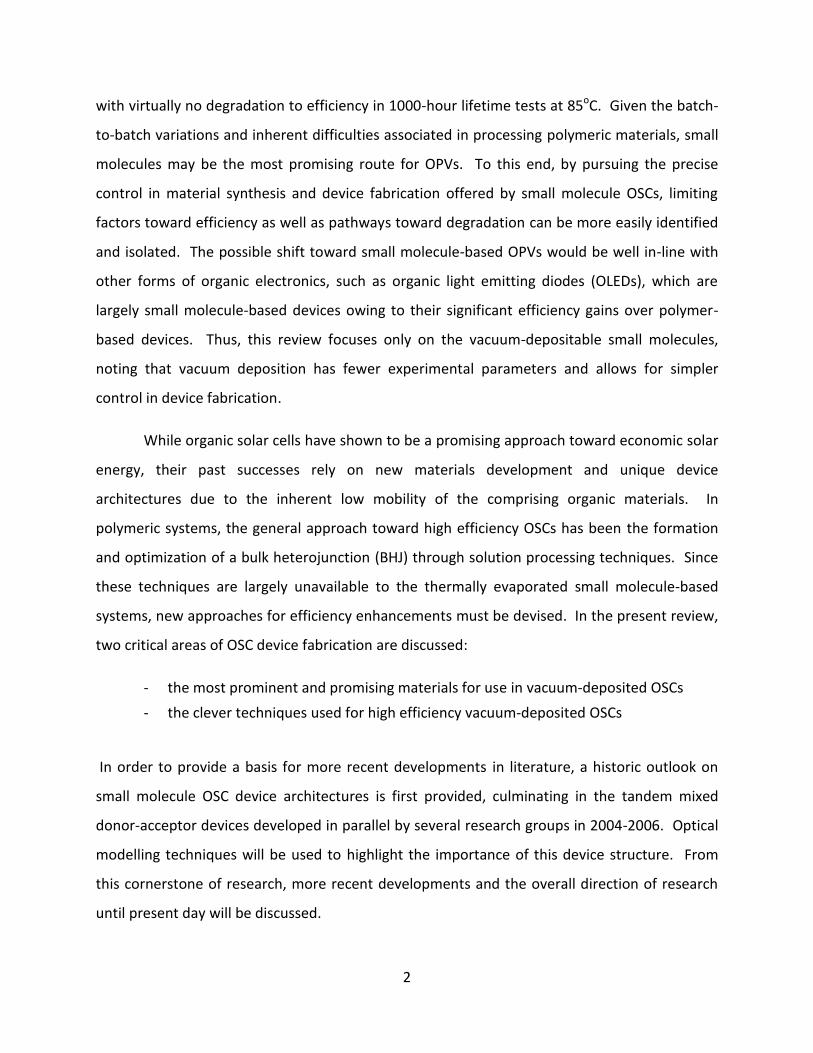
2. Small Molecule Organic Solar Cells: Early Developments
Initial work
on small molecule
OSCs focused on the
study of bilayer
devices, following
the success of Tang
in 1986 [15]. In this
research, Tang
proposed a planar
heterojunction (PHJ)
comprised of an electron donating material and an electron accepting material. The lowest
unoccupied molecular orbital (LUMO) and highest occupied molecular orbital (HOMO) of the
donor and acceptor are offset to allow for splitting of photogenerated excitons into electrons
and holes. In Tang’s work, the donor material was copper phthalocyanine (CuPc) and the
acceptor material was 3,4,9,10-perylenetetracarboxylic bis-benzimidazole (PTCBI). An
illustration of a simple device based on this architecture along with the relevant energy levels is
shown in Figure 1. The most significant variation to this device is the replacement of PTCBI with
fullerene (C60) as the acceptor material and the occasional substitution of CuPc for Zinc
Phthalocyanine (ZnPc).
In any photovoltaic device, it is necessary to separate photo-generated excitons into
electrons and holes, and to collect these free carriers before they recombine. For the
aforementioned CuPc-PTCBI device, this process is accomplished as described below and
illustrated in Figure 1:
i. an impingent photon produces an exciton in either the CuPc or PTCBI layer
ii. the exciton diffuses to the CuPc-PTCBI interface to be separated into its constituent
electron and hole
iii. the free carriers are subsequently collected at their relevant electrodes
Figure 1 - A. Illustration of a Simple Planar Heterojunction Device Comprised of CuPc Donor and PTBI Acceptor. B. Associated Energy Levels
of the CuPc/PTCBI Device with Illustration of Light Harvesting Action.

4
Unfortunately, the exciton diffusion length for organic materials is generally very low. When
considering a simple bilayer OSC, the exciton diffusion length is generally much smaller than the
layer thicknesses required for efficient absorption of light. For example, one may use a 100nm
CuPc absorbing layer; however, only excitons formed within 10nm of the CuPc-PTCBI junction
will result in collectable electrons and holes [16]. In order to address this problem, two
approaches have been suggested: multiple or tandem solar cells, and mixed layer solar cells –
analogous to the bulk heterojunction used in polymer solar cells.
2.1. Multiple and Tandem Solar Cells
The ultimate goal of stacking PHJ solar cells in a tandem configuration is to have many
interfaces for efficient exciton dissociation while maintaining a summative thick film for
absorption of light. One may also absorb a broader spectrum of light through the use of
different donor/acceptor materials with different absorption characteristics. Since stacked
solar cells are effectively in series, they ideally have an open circuit voltage (VOC) equal to the
sum of the Voc values of the individual sub-cells. However, the short circuit current density (Jsc)
is effectively limited by the sub-cell with the lowest Jsc. The obvious downside of tandem solar
cells is the increased complexity to device fabrication and associated increase in costs with each
additional layer.
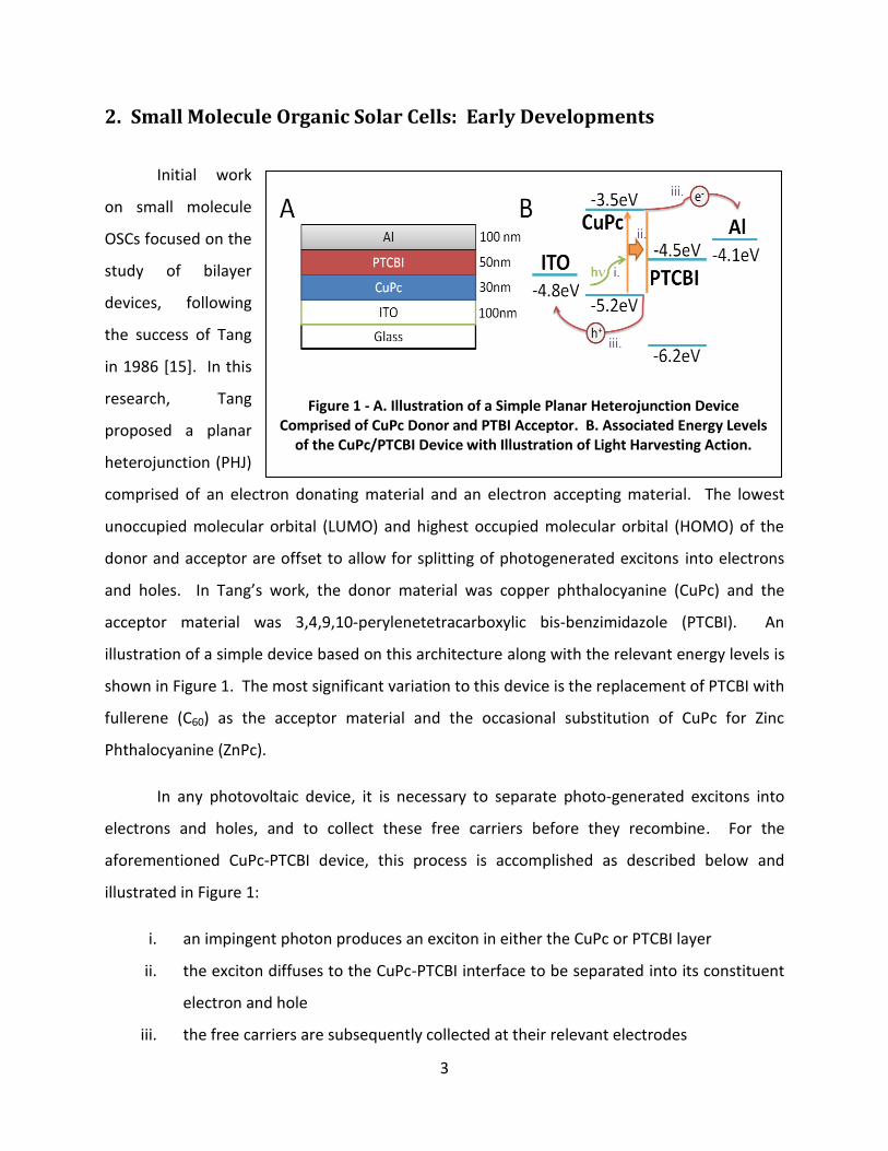
Following this rationale,
Peumans, Yakimov and Forrest
examined multiple junction OSCs
based on CuPc-PTCBI PHJs [16,
17]. An example two-stack PHJ
OSC is shown in Figure 2.
Deposition of two CuPc-PTCBI
devices in series would intuitively
result in the formation of an
inverse heterojunction. As such,
Figure 2 - Illustration of a Double Planar Heterojunction (Tandem) Solar Cell. Image adapted from Ref [16].
5
the researchers made use of an ultrathin (ideally 5Å) silver layer to separate neighbouring
heterojunctions. At 5Å thickness, the silver layer forms islands that act as efficient
recombination centres. In this manner, holes from CuPc recombine directly with electrons from
PTCBI on the silver islands. As long as the rate of recombination surpasses the generation rate
of free carriers, there is no charge accumulation at this interface so there is no splitting of the
quasi-Fermi levels and no formation of the inverse heterojunction. Further, it is supposed that
carriers tunnel through interface dipoles at the metal island-organic interfaces (shown, for
example, at the PTCBI-Ag interface in Figure 2) [16]. The function of the multijunction OSC is
then as follows:
- Impingent light generates excitons in both the front and back cells
- The excitons are split into electrons and holes at the two CuPc-PTCBI interfaces
- The hole from the front cell is collected at the ITO contact and the electron from the
back cell is collected at the Ag contact
- The remaining electron in the front cell recombines with the remaining hole from
the back cell at the ultra-thin Ag layer
In effect, one generates photocurrent equivalent to a single cell; however, as illustrated in
Figure 2, the Voc of the multijunction OSC is the sum of the individual Voc values.
As a point of note, the stacking of cells cannot be repeated ad infinitum to achieve
unrealistically high open circuit voltage values. From the work in [17], the OSC with two
stacked cells performed best at 1-sun illumination, achieving optimal VOC and associated power
conversion efficiency (PCE) values of (2.5% PCE1) when compared to 3-cell and 5-cell OSCs. As
more cells are stacked, less light reaches the lower cells due to absorption of light from the
active CuPc/PTCBI layers and due to scattering or absorption of light by the Ag layers. As a
consequence, 5-cell OSCs, for example, would have to be run at unrealistically high light
intensities (>10 suns) to achieve peak efficiencies. In order to achieve such high light intensities
solar concentrators would be required, which would drastically increase the cost of the solar
cell and thus make any economic gains from using organic materials irrelevant.
1 All PCE values throughout this review are quoted for AM1.5, 100mW/cm
2 (1-sun) exposure unless specified
otherwise
6
2.2. Mixed Layer and Bulk Heterojunction Solar Cells
The common route to high efficiency polymer OSCs is the formation of the BHJ, which
comprises an active layer with mixed donor and acceptor species to allow for much thicker
films to better absorb sunlight. Thick films are possible because excitons will encounter donor-
acceptor interfaces with much higher probability, as these interfaces are distributed throughout
the entire active layer. This approach is prevalent in polymer OSCs given its ease in
implementation for solution-based fabrication – one can simply mix the donor and acceptor
species in the same solvent prior to doctor blading, spin-coating or spray-coating. It is also a
proven approach for small molecule OSCs, although there are significantly fewer variables
available to control the ultimate morphology of the mixed donor-acceptor layer.
The obvious downside of the bulk heterojunction is that the hole and electron mobilities
in the mixed layer are significantly reduced compared to the pure donor and acceptor layers.
Further, for a hole or an electron to be collected, they must be generated in a region of donor
or acceptor that is continuous to the anode or cathode. ‘Dead ends’ can lead to undesirable
charge accumulation and carrier recombination that ultimately decrease the solar cell
efficiency. The morphology of the mixed layer is thus very important and incredibly susceptible
to experimental variation. An ideal morphology is a bicontinuous distribution of donor and
acceptor phases, with pure phases on the order of nanometres for efficient exciton separation.
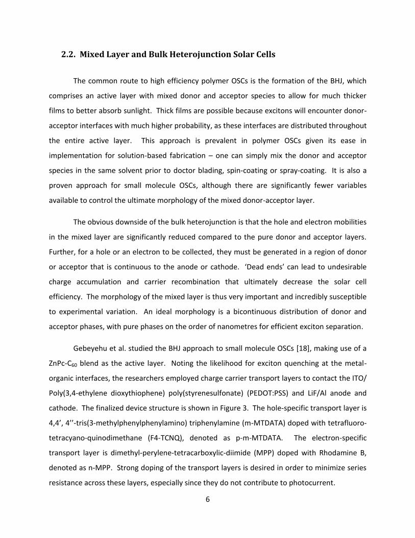
Gebeyehu et al. studied the BHJ approach to small molecule OSCs [18], making use of a
ZnPc-C60 blend as the active layer. Noting the likelihood for exciton quenching at the metal-
organic interfaces, the researchers employed charge carrier transport layers to contact the ITO/
Poly(3,4-ethylene dioxythiophene) poly(styrenesulfonate) (PEDOT:PSS) and LiF/Al anode and
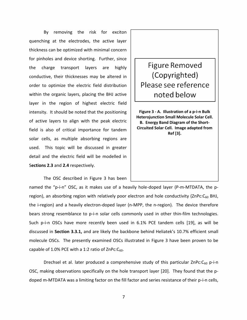
cathode. The finalized device structure is shown in Figure 3. The hole-specific transport layer is
4,4’, 4’’-tris(3-methylphenylphenylamino) triphenylamine (m-MTDATA) doped with tetrafluoro-
tetracyano-quinodimethane (F4-TCNQ), denoted as p-m-MTDATA. The electron-specific
transport layer is dimethyl-perylene-tetracarboxylic-diimide (MPP) doped with Rhodamine B,
denoted as n-MPP. Strong doping of the transport layers is desired in order to minimize series
resistance across these layers, especially since they do not contribute to photocurrent.
7
By removing the risk for exciton
quenching at the electrodes, the active layer
thickness can be optimized with minimal concern
for pinholes and device shorting. Further, since
the charge transport layers are highly
conductive, their thicknesses may be altered in
order to optimize the electric field distribution
within the organic layers, placing the BHJ active
layer in the region of highest electric field
intensity. It should be noted that the positioning
of active layers to align with the peak electric
field is also of critical importance for tandem
solar cells, as multiple absorbing regions are
used. This topic will be discussed in greater
detail and the electric field will be modelled in
Sections 2.3 and 2.4 respectively.
The OSC described in Figure 3 has been
named the “p-i-n” OSC, as it makes use of a heavily hole-doped layer (P-m-MTDATA, the p-
region), an absorbing region with relatively poor electron and hole conductivity (ZnPc:C60 BHJ,
the i-region) and a heavily electron-doped layer (n-MPP, the n-region). The device therefore
bears strong resemblance to p-i-n solar cells commonly used in other thin-film technologies.
Such p-i-n OSCs have more recently been used in 6.1% PCE tandem cells [19], as will be
discussed in Section 3.3.1, and are likely the backbone behind Heliatek’s 10.7% efficient small
molecule OSCs. The presently examined OSCs illustrated in Figure 3 have been proven to be
capable of 1.0% PCE with a 1:2 ratio of ZnPc:C60.
Drechsel et al. later produced a comprehensive study of this particular ZnPc:C60 p-i-n
OSC, making observations specifically on the hole transport layer [20]. They found that the p-
doped m-MTDATA was a limiting factor on the fill factor and series resistance of their p-i-n cells,
Figure 3 - A. Illustration of a p-i-n Bulk Heterojunction Small Molecule Solar Cell.
B. Energy Band Diagram of the Short-Circuited Solar Cell. Image adapted from
Ref [3].
8
and therefore switched to the higher conductivity N,N,N’,N’-tetrakis(4-methoxyphenyl)-
benzidine (MeO-TPD). The researchers also stressed the importance of forming an Ohmic
contact between the organic layers and the adjacent organic layers, noting the strong likelihood
for dopant degradation with top-contact deposition. In order to avoid such degradation, a thin,
protective layer prior to top contact deposition was found to be desirable. Based on these
modifications and observations, the resulting ZnPc:C60 p-i-n OSC allowed for a 1.9% PCE [20].
In a similar vein, Uchida et al. investigated CuPc:C60 bulk heterojunction devices [21].
The researchers noted a marked improvement in PCE by inclusion of a neat C60 layer between
the CuPC:C60 BHJ and the top electrode, effectively forming a pseudo-'i-n' device. In this work,
they made use of a 2,9-dimethyl-4,7-diphenyl-1,10-phenanthroline (BCP) hole/exciton blocking
layer, which has a deep HOMO to block holes and to preclude exciton quenching at the top
contact. BCP serves a secondary purpose to protect
the neat C60 layer from damage during Ag
evaporation. Optimization of their layer thicknesses
allowed for 3.5% PCE and a notably smaller series
resistance when compared to the ZnPc:C60 devices by
Drechsel et al [20].
Following their successes in [21] and using the
same reasoning as applied with the p-i-n devices, Xue
et al. investigated their hybrid planar-mixed
molecular heterojunction (PM-HJ), as illustrated in
Figure 4 [22, 23]. In this case, instead of using heavily
doped transport layers, Xue et al. simply extended
pure CuPc and C60 layers from the mixed BHJ. This
device structure may be considered a subset of the p-
i-n device structure considered earlier, but the use of
pure donor and acceptor ‘p’ and ‘n’ layers to border
the mixed layer is ineffective in blocking excitons.
Figure 4 - A. Device Structure of the Planar-Mixed Molecular Heterojunction.
B. Image of the Band Structure for the Same. Image adapted from Ref [8].
9
Further, the absence of dopants in these layers results in increased series resistances. The
benefit of the PM-HJ is that the pure CuPc and C60 layers also contribute to photocurrent. If the
transport layers are designed to have thicknesses equal to the exciton diffusion lengths, most
excitons will reach a donor-acceptor interface for dissociation. As with their previous work, BCP
was used to block holes and excitons and to prevent damage to the organic layers during
evaporation of the silver contact. The optimized solar cells from this work achieved 5% PCE.
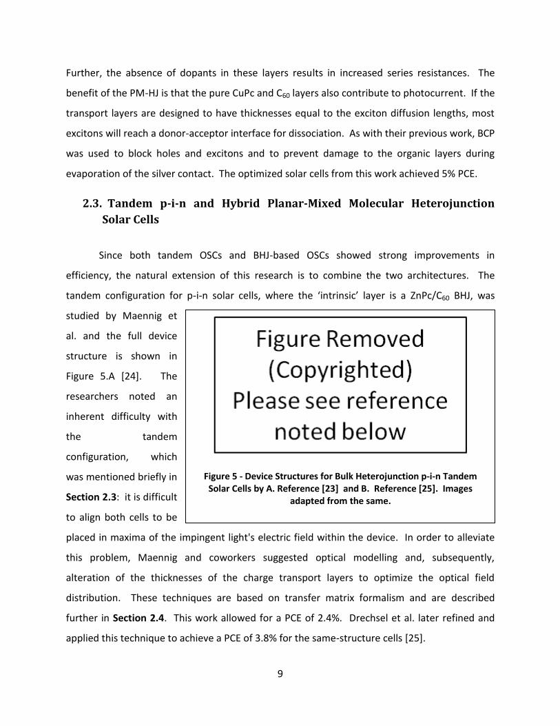
2.3. Tandem p-i-n and Hybrid Planar-Mixed Molecular Heterojunction
Solar Cells
Since both tandem OSCs and BHJ-based OSCs showed strong improvements in
efficiency, the natural extension of this research is to combine the two architectures. The
tandem configuration for p-i-n solar cells, where the ‘intrinsic’ layer is a ZnPc/C60 BHJ, was
studied by Maennig et
al. and the full device
structure is shown in
Figure 5.A [24]. The
researchers noted an
inherent difficulty with
the tandem
configuration, which
was mentioned briefly in
Section 2.3: it is difficult
to align both cells to be
placed in maxima of the impingent light's electric field within the device. In order to alleviate
this problem, Maennig and coworkers suggested optical modelling and, subsequently,
alteration of the thicknesses of the charge transport layers to optimize the optical field
distribution. These techniques are based on transfer matrix formalism and are described
further in Section 2.4. This work allowed for a PCE of 2.4%. Drechsel et al. later refined and
applied this technique to achieve a PCE of 3.8% for the same-structure cells [25].
Figure 5 - Device Structures for Bulk Heterojunction p-i-n Tandem Solar Cells by A. Reference [23] and B. Reference [25]. Images
adapted from the same.
10
Xue and coworkers pursued a similar tandem device structure based off of their PM-HJ
device structure. The tandem device is illustrated in Figure 5.B, where they separate the two
cells by a PTCBI/Ag cluster/m-MTDATA stack [26]. The Ag cluster stack buried in m-MTDATA
acts as an efficient recombination centre. Since CuPc absorbs at ~550nm-750nm and C60
absorbs at ~350nm-550nm, the researchers proposed asymmetric thicknesses of the sub-cells,
where the front cell absorbs short wavelengths (thicker pure C60 layer) and the back cell
absorbs long wavelengths (thicker pure CuPc layer). By optimizing the optical field distribution,
taking this asymmetry into consideration, Xue et al. were able to achieve 5.7% PCE.
Note that in a very brief period of time the proposed structure for the OSC
encompassed four major avenues of device structure: planar heterojunction, tandem planar
heterojunction, bulk heterojunction and tandem bulk heterojunction. The bulk heterojunction
may be further broken down into the simple BHJ and the p-i-n heterojunction. A simple
variation of the p-i-n heterojunction, denoted as the PM-HJ, relies on extending the individual
components of the BHJ as pure layers to border the BHJ. By incorporating this PM-HJ into a
tandem device, researchers ultimately achieved 5.7% PCE [26], which remains one of the
highest efficiencies for small molecule OSCs reported in literature.
2.4. Optical Modelling of Organic Solar Cells by Transfer Matrix Formalism
Optical modelling of OSCs can be accomplished by transfer matrix formalism, which is
detailed in a more rigorous manner in Appendix A2. As noted previously, optical modelling
allows for placement of the peak electric field in the 'active region' of the device – generally the
regions comprising of either, or both of, the donor or the acceptor. Shifting the optical field can
be accomplished by use of thick optical spacer layers comprised of high conductivity inorganic
semiconductors [27], or heavily doped materials [19]. The optical spacers must ideally avoid
significant increases to the series resistance of the devices. Since the generation of excitons is
proportional to the intensity of the impingent optical field, this is a simple and cost-effective
approach to drastically improve the efficiency of OSCs.
2 Note: Appendix A was completed for the extra modelling assignment for ECE632
11
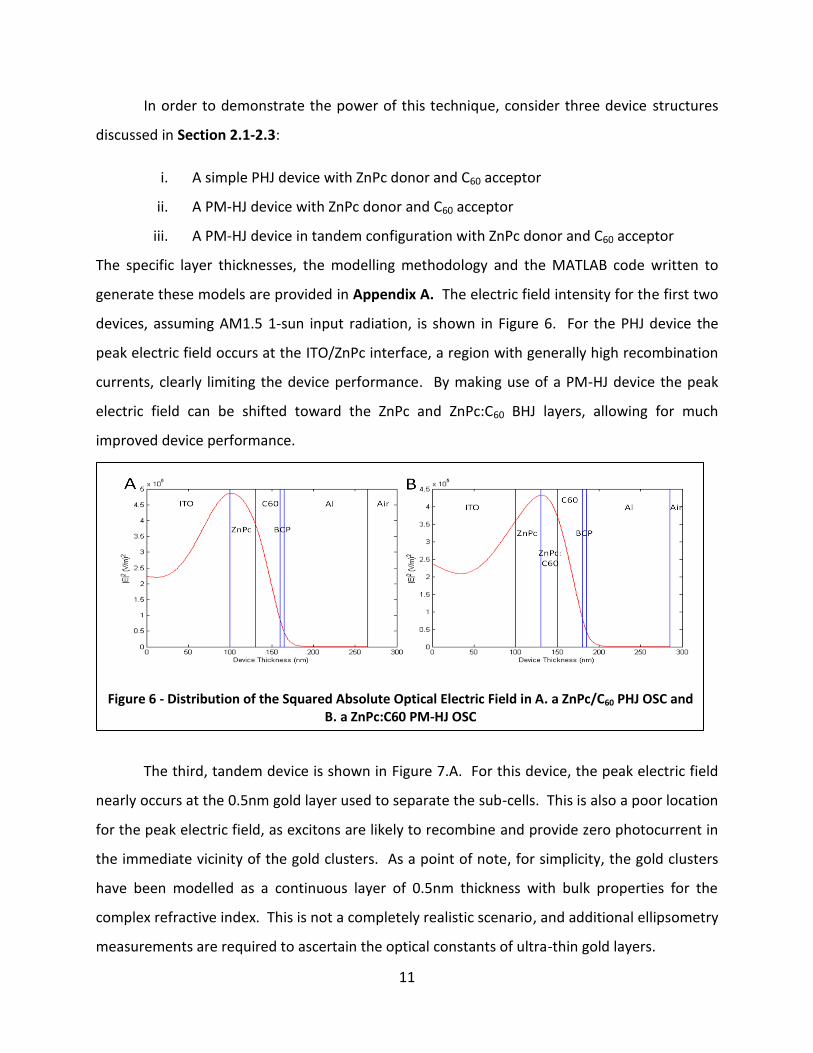
In order to demonstrate the power of this technique, consider three device structures
discussed in Section 2.1-2.3:
i. A simple PHJ device with ZnPc donor and C60 acceptor
ii. A PM-HJ device with ZnPc donor and C60 acceptor
iii. A PM-HJ device in tandem configuration with ZnPc donor and C60 acceptor
The specific layer thicknesses, the modelling methodology and the MATLAB code written to
generate these models are provided in Appendix A. The electric field intensity for the first two
devices, assuming AM1.5 1-sun input radiation, is shown in Figure 6. For the PHJ device the
peak electric field occurs at the ITO/ZnPc interface, a region with generally high recombination
currents, clearly limiting the device performance. By making use of a PM-HJ device the peak
electric field can be shifted toward the ZnPc and ZnPc:C60 BHJ layers, allowing for much
improved device performance.
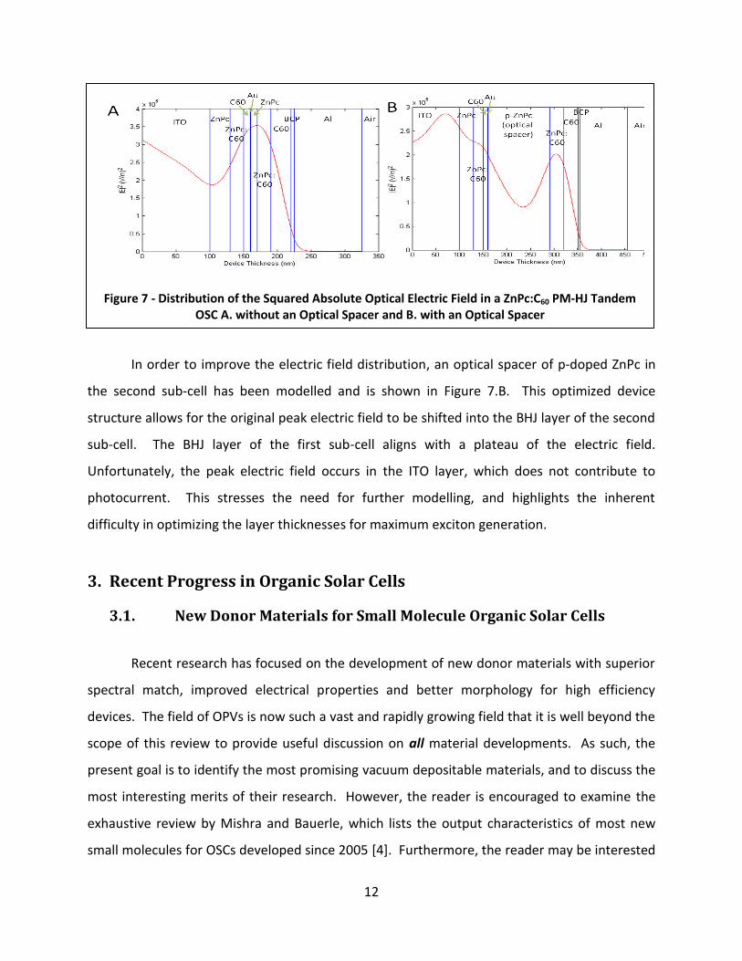
The third, tandem device is shown in Figure 7.A. For this device, the peak electric field
nearly occurs at the 0.5nm gold layer used to separate the sub-cells. This is also a poor location
for the peak electric field, as excitons are likely to recombine and provide zero photocurrent in
the immediate vicinity of the gold clusters. As a point of note, for simplicity, the gold clusters
have been modelled as a continuous layer of 0.5nm thickness with bulk properties for the
complex refractive index. This is not a completely realistic scenario, and additional ellipsometry
measurements are required to ascertain the optical constants of ultra-thin gold layers.
Figure 6 - Distribution of the Squared Absolute Optical Electric Field in A. a ZnPc/C60 PHJ OSC and B. a ZnPc:C60 PM-HJ OSC
12
In order to improve the electric field distribution, an optical spacer of p-doped ZnPc in
the second sub-cell has been modelled and is shown in Figure 7.B. This optimized device
structure allows for the original peak electric field to be shifted into the BHJ layer of the second
sub-cell. The BHJ layer of the first sub-cell aligns with a plateau of the electric field.
Unfortunately, the peak electric field occurs in the ITO layer, which does not contribute to
photocurrent. This stresses the need for further modelling, and highlights the inherent
difficulty in optimizing the layer thicknesses for maximum exciton generation.
3. Recent Progress in Organic Solar Cells
3.1. New Donor Materials for Small Molecule Organic Solar Cells
Recent research has focused on the development of new donor materials with superior
spectral match, improved electrical properties and better morphology for high efficiency
devices. The field of OPVs is now such a vast and rapidly growing field that it is well beyond the
scope of this review to provide useful discussion on all material developments. As such, the
present goal is to identify the most promising vacuum depositable materials, and to discuss the
most interesting merits of their research. However, the reader is encouraged to examine the
exhaustive review by Mishra and Bauerle, which lists the output characteristics of most new
small molecules for OSCs developed since 2005 [4]. Furthermore, the reader may be interested
Figure 7 - Distribution of the Squared Absolute Optical Electric Field in a ZnPc:C60 PM-HJ Tandem OSC A. without an Optical Spacer and B. with an Optical Spacer
13
in one of several reviews on the synthesis of new soluble small molecule OSC materials [1-3],
the most recent of which is quite extensive.
Following the successes of CuPc and ZnPc, many groups investigated other metal-
phthalocyanines for applications in OSCs. Yuen et al. examined a large subset of these
materials in unoptimized PHJs and BHJs, including metal-free Pc, MgPc, AlClPc, GaClPc, ClInPc,
TiOPc and VOPc [28]. Wang et al. focused on TiOPc and ClInPc donors specifically, noting their
strong sensitivity to solvent annealing treatments [29]. In particular, OSCs made from both
TiOPc and ClInPc exhibited substantially improved device properties with when exposed to a
chloroform vapour – TiOPc PHJ devices shifted from 1.3% to 3% PCE and ClInPc PHJ devices
shifted from 2.6% PCE to 3.3% PCE. The authors attribute this improvement to the increased
roughness with solvent annealing, which is purported to increase the contact area with C60 in a
PHJ device configuration. Chloroform-based solvent annealing was also shown to red-shift the
absorption band of TiOPc films, but had little effect on the absorption properties of ClInPc films.
In a similar vein,
Bamsey et al. employed
tetrahydrofuran (THF) instead
of chloroform solvent
annealing on ClInPc films and
noted a strong red-shift in the
ClInPc absorption band as
well as the EQE spectra, as
shown in Figure 8.C [30]. The
researchers used this
technique to create a
heteromorphic film, where
the first portion of the ClInPc
film was deposited and
solvent annealed, and the second portion was subsequently deposited without solvent
Figure 8 - A. Illustration of a ClInPc/C60 PHJ OSCs with 3 Types of ClInPc Films with Different Solvent Treatments. B. Associated IV
Characteristics of the ClInPC/C60 PHJ OSCs. C. Associated EQE Spectra of the Same. Figure adapted from Ref. [33].
14
annealing. This is illustrated in Figure 8.A.III. The resulting device thus exhibited a broad
absorption spectrum, spanning both the absorption of the un-annealed film and the annealed
film, and had improved device characteristics, as shown in Figure 8.B. As a point of interest, the
Voc of this device was found to be in between that of the un-annealed and the annealed device.
Fujishima et al. studied tetraphenyldibenzoperiflanthene (DBP) as a replacement to Pc
species for the acceptor material [31]. The authors note DBP’s strong absorption throughout
500-600nm, which aligns well with the peak emission from the solar spectrum. DBP further
exhibits a HOMO at 5.5eV compared to the 5.2eV of CuPc. In general, the theoretical maximum
Voc can be found as the difference between the HOMO of the donor and the LUMO of the
acceptor. Given a LUMO of 4.5eV for C60, the maximum Voc for CuPc-based cells is 0.7V, while
the maximum Voc for DBP cells is 1V. Experimentally, the authors observed an improvement
from 0.7V to 0.9V when switching from CuPc/C60 to DBP/C60 PHJ OSCs. The highest PCE
observed for DBP/C60 PHJ cells was found to be 3.6%.
Wagner et al. focused on diindenoperylene (DIP) to improve upon the inherent charge
transport limitations of CuPc:C60 and ZnPc:C60 blends. DIP is a perylene derivative with
absorption peaks spanning a large portion of the visible spectrum, from 375nm to 550nm with
tail-end absorption extending beyond 600nm. The researchers sought improved electrical
properties of their DIP films through improved morphology, which they found could be
controlled strongly by varying substrate temperature during deposition. An optimal substrate
temperature of 100oC was found. PHJ devices employing a C60 acceptor were shown to have a
PCE of 3.9% with a very high fill factor of 74.3% and a strong Voc of 0.9V. The impressive fill
factor is proof of the high quality of the deposited film – in particular, its high hole mobility and
low concentration of trap states.
Forrest and coworkers, (creators of the PM-HJ OSC and the 5.7% PCE tandem PM-HJ
OSCs [26]), shifted their focus toward squaraines and their derivatives. Wang et al. synthesized
2,4-bis[4-N,N-diisobutylamino-2,6-dihydroxyphenyl] squaraine (SQ), which exhibits a strong
absorption peak at ~700nm [32]. The authors note that further modification of the amine
donors or the aryl groups can allow for absorption into the near-IR – up to 1000nm. The
15
presently examined SQ was chosen due to its capacity to withstand molecular degradation
during sublimation, allowing it to be vacuum deposited. Further, this SQ has a relatively deep
HOMO (5.3eV), which allows for a large Voc. OSCs were fabricated with the structure:
IT/SQ/C60/BCP/Al. 3.2% PCE cells were attained for the thinnest SQ layer thicknesses (65-110Å).
Further studies on squaraines are detailed in Section 3.2 and Section 3.3.
Several groups have investigated triphenylamine (TPA) derivative donors to improve
reproducibility of their OSCs by removing direction-dependent transport properties [33-35].
TPA has a unique propeller-like structure, which is responsible for its glass-like or amorphous
film-forming properties, as illustrated in Figure 9. As such, it is feasible to obtain a reasonable
degree of isotropy in carrier mobility, which makes TPA simple to incorporate into both vertical
and lateral device structures. Cravino et al. ([33]) specifically examined
thienylenevinylenetriphenylamin
e functionalized with peripheral
dicyanovinylene groups (TDCV-
TPA) with the following
molecular design goals:
- create an internal
charge transfer to
shift the TPA
absorption band to
better match the solar
spectrum
- preserve or enhance the high oxidation potential (deep HOMO) of TPA
- achieve high hole mobility
Their unoptimized TDCV-TPA/C60 PHJ achieved a PCE of 1.9% with a very high Voc of 1.2V. This
is attributed to the as-designed HOMO of 6eV for TDCV-TPA that allows for a theoretical
maximum Voc of 1.5V. It is feasible that the Voc of these devices could be improved even
further. More recently, Kagayama et al. ([34]) examined tris[4-(5-phenylthiophen-2-
Figure 9 - Illustrations of TPA Derivatives, including A. TDCV-TPA (Ref. [36]) and B. TPTPA (Ref. [37]).
16
yl)phenyl]amine (TPTPA) as a donor, which exhibits absorption in the 400nm range. When
incorporated into a PHJ with C70, the researchers achieved a PCE of 2.2% and Voc values of 0.9V.
Roquet et al. ([35]) examined a TPA derivative with thienylenevinylene conjugated
branches and electron-withdrawing indanedione or dicyanovinyl groups. Depending on their
solubility, these TPA derivatives were used in either solution-coated BHJ cells with a PCBM
acceptor or vacuum-deposited PHJ cells with a C60 acceptor. The authors showed that they
could easily tune the EQE spectra by altering one arm of the TPA base molecule. To this end,
they observed a shift in the peak response from 480nm to 550-580nm by functionalizing one
TPA arm with an indanedione or malononitrile group. The HOMO of TPA derivative was also
shown to be tunable, allowing for a maximum Voc of 0.96V.
Lloyd and coworkers studied (triisopropylsilylethynyl)pentacene (TIPS-pentacene) due
to the ~50nm bathochromic shift of its primary absorption peak compared to the well-studied
pentacene [36]. TIPS-pentacene further exhibits a HOMO that is 0.28eV lower than that of
pentacene, allowing for an improved Voc when coupled with C60. With proper thermal
annealing treatments, TIPS-pentacene was shown to form crystallites and provide high hole
mobility, in much the same manner as pentacene (in spite of the TIPS functionalization). While
TIPS-pentacene dissolved in toluene, it was insoluble in more common organic solvents such as
chloroform, chlorobenzene and dichlorobenzene. As such, the researchers spun thin films of
TIPS-pentacene and subsequently vacuum-deposited C60 to create PHJ devices. In spite of
various optimization approaches, devices only showed a maximum PCE of 0.5% PCE.
Noting the success of thiophenes in P3HT:PCBM solar cells, many researchers studied
oligomers based on thiophenes. In contrast to their polymeric counterparts, oligomers are
comprised of less than twenty monomer units, and are thus much easier to fabricate and purify
in a controlled manner. In an idealized scenario, they may offer the improved conductivity and
film-forming properties of polymers, but have the control and reproducibility of small
molecules. Xia et al. studied Triarylamino and Tricyanovinyl as well as Diarylamino and
Dicyanovinyl End-Capped Oligothiophenes (PhN-OFOT(2,3)-TCN) and diPhN-OFOT(2,3,4)-DCN
respectively) [37, 38]. The indices (2,3) and (2,3,4) indicate the number of monomer units
17
within the oligomer chain (for example, PhN-OFOT(3)-TCN) is a 3-unit oligomer). The PhN-
OFOT(2,3)-TCN species showed a strong absorption peak at ~680-690nm and a broad shoulder
at ~530nm, while diPhN-OFOT(4)-DCN had absorption peaks at ~450nm and ~580nm. As with
P3HT-based OSCs, these thiophene oligomers showed strong improvements to morphology
with thermal annealing that allowed for improved electrical characteristics when incorporated
into PHJ OSCs. The maximum PCEs for PhN-OFOT(2)-TCN and diPhN-OFOT(4)-DCN PHJ OSCs
(formed with a C60 acceptor) were 1.3% and 2.67% respectively. While the Voc values for both
species were quite high at 0.8 to 0.9V, the fill factors remained quite low at 40-50%, limiting
device efficiency.
3.2. Novel Fabrication Techniques for Small Molecule Organic Solar Cells
Substantial efforts have been dedicated to enhancing the PCE of small molecule OSCs
through specialized fabrication techniques. The most basic techniques involve improving film
morphology through substrate heating during deposition, or by thermal annealing treatments
and solvent annealing treatments. For solvent annealing treatments, the deposited film is
exposed to a solvent-saturated environment to change the film morphology. More recently,
researchers have investigated more esoteric approaches to improving device efficiency. Some
of the more successful approaches are detailed throughout this section.
Tandem OSCs can provide significant PCE improvements by implementation of different
donor/acceptor combinations for better spectral match to the solar spectrum. However, as
noted in Section 2.1, these devices suffer from substantially increased device complexity and
device costs. In order to address this limitation, Yuen et al. examined a simple parallel device
structure employing multiple donor species in a mixed/planar device structure [39]. A
representative parallel device structure is shown in Figure 10, along with the device’s energy
levels. Yuen and coworkers first deposited a thin layer of ZnPc to allow for strong light
absorption at ~620nm. A mixed ClInPc:C60 layer was subsequently deposited to allow for strong
light absorption at ~730nm. In regular device operation, photogenerated electrons from ZnPc
are transferred to the C60 in the ClInPc:C60 layer and subsequently to the pure C60 layer to be
collected at the Al cathode, whereas holes are transferred to the ITO directly. The ClInPc:C60
18
layer forms a BHJ, where
photogenerated electrons
are transferred to C60/Al
and holes easily flow
through the thin ZnPc layer
to be collected at the ITO
anode. The result is a
device that offers higher Jsc
than either the ZnPc/C60
PHJ device or the ClInPc:C60 BHJ device alone, and a Voc in between the Voc values of the
constituent devices. As a consequence, the parallel device offers a substantially improved PCE
of 1.8%, compared to 0.9% for the ZnPc/C60 PHJ OSC and 1.3% for the ClInPc:C60 BHJ OSC.
A similar approach was applied by Wong et al. with a ‘CuPc/rhenium benzathiazole
complex:C60/C60’ device [40]. In this manner, CuPc allowed for absorption over 600-800nm,
while the rhenium complex provided absorption in the range of 400-500nm. The EQE of these
cells exhibited reasonably strong absorption over most of the visible range, with only a slight
valley in the 500-550nm region. These OSCs were shown to be capable of 1.72% PCE. Kim et al.
also employed this methodology, by swapping the pure ZnPc layer in a ZnPc:C60 PM-HJ with a
PdPc layer to extend the absorption range of the OSC [41]. Their finalized structure was:
‘ITO/PdPc/ZnPc:C60/C60/ N,N′-dihexyl-perylene-3,4,9,10-bis(dicarboximide) PTCDI-C6/BCP/Ag’.
The researchers observed strong improvements to the EQE, with visible photocurrent
contributions from both the ZnPc and the PdPc species. This allowed for an increase in PCE
from 3.2% for the PM-HJ ZnPc:C60 cell to 3.7% for a PdPc/ZnPc:C60/C60 cell.
In the work by Kim et al. [41], as well as subsequent studies in [42], PTCDI-C6 was used
as an interlayer between C60 and the traditional hole/exciton blocking layer, BCP. The inclusion
of the PTCDI-C6 layer improved Jsc by improving the EQE across all wavelengths in the visible
spectrum. The use of PTCDI-C6 was also shown to drastically reduce device sensitivity to the
thickness of the BCP layer. For devices without PTCDI-C6, BCP thicknesses greater than 10nm
Figure 10 - A. Illustration of the Parallel Device Structure B. Energy Levels of the Same. B Adapted from Ref. [42].
19
drastically reduce the FF and Jsc. In contrast, devices with PTCDI-C6 can have BCP thicknesses
up to 20nm before device performance is negatively affected.
One may consider several reasons for the decreased OSC performance with increasing
BCP thicknesses:
- BCP has a very low LUMO, which may hinder collection of electrons with the
formation of a continuous BCP film at larger film thicknesses
- At higher film thicknesses, BCP may be more prone to unfavourable partial
crystallization that results in the formation of grain boundaries and trap states
- the deposition of the top metal electrode results in metal doping of the BCP layer,
which would be less prevalent at larger BCP film thicknesses
The deposition of PTCDI-C6 was shown to substantially increase the surface roughness, which
could be reasoned to address any of the above theories. More specifically, with higher surface
roughness, the ‘effective thickness’ of the BCP layer is reduced.
Noting the improvements made to OSC efficiency by insertion of inter-layers at the
organic-cathode interface, Hirade et al. sought to study and improve upon the organic-anode
interface [43]. As a first point of interest, the researchers show that the traditional hole-
extraction layer, PEDOT:PSS, is an efficient exciton quencher that can substantially reduce
device performance. As such, Hirade and coworkers employed TPTPA as an electron and
exciton blocking layer due to its much larger energy gap of 2.7eV compared to the energy gap
of the chosen donor, DBP. Since TPTPA has a comparable HOMO to that of DBP and a hole
mobility exceeding DBP, no substantial losses to device performance were expected. Insertion
of TPTPA into DBP/C60 PHJ device granted a substantial improvement in Jsc and a slight
improvement in FF, resulting in a shift in PCE from 3.9% to 5.3%. This improvement was
verified to be purely due to exciton blocking effects and not due to morphological variations, as
no variations in the active layer structure were observed by x-ray diffraction and
photoluminescence measurements.
20
Beyond the insertion of additional sensitizing and carrier extraction/blocking layers,
many efficiency enhancement techniques have been dedicated to the improvement of the
donor/acceptor morphology and crystallinity. In order to achieve nanoscale phases of pure
donor and acceptor in their BHJs, Sakai et al. alternated deposition of very thin layers of donor
(D) and acceptor (A) to form a
‘DADADA. . .’ stack [44]. The
researchers used 1-2nm of
pentacene and C60 for the
donor and acceptor
respectively. The stack is
illustrated in Figure 11 along
with a cross-sectional scanning
electron microscope (SEM)
image. Since these films are
not perfectly continuous at 1-
2nm, their alternating
deposition results in the
formation of an interpenetrating bicontinuous network. Sakai and coworkers substituted a 12-
layer ‘DA’ stack for the mixed layer in a PM-HJ OSC to obtain the following device structure:
ITO/PEDOT:PSS/Pentacene(20 nm)/ [C60(2nm)/Pentacene(2nm]6 /C60/BCP/MgAg
This OSC achieved a PCE of 1.58%, which is a 68% improvement over the PCE of a simple
pentacene/C60 PHJ OSC. The improvement was attributed to a substantial increase in
conversion of excitons into electrons and holes. This improvement is reasonable, as the spacing
between pure pentacene and C60 phases is on the order of 1-2nm, which is much lower than
the exciton diffusion lengths for these materials. Increasing the number of stack layers beyond
twelve served to increase the series resistance, which deteriorated the PCE.
Yang and coworkers followed a similar approach, instead using CuPc as the donor and
C60 as the acceptor in a ‘DADADA. . .’ stack [45]. The authors note the preferable formation of
Figure 11 - Illustration of the Pentacene-C60 Repeating Donor-Acceptor Stack Architecture with a Cross-Sectional SEM Image
of the Same. Figure adapted from Ref. [47].
21
pure C60 and pure CuPc crystalline domains due to the relatively large C60-C60 and CuPc-CuPc
interaction energies versus those of the CuPc-C60 molecular pair. At a 12-layer ‘DA’ stack (6 of
donor and 6 acceptor layers), the interfacial area was found to be 11-times that of a simple
bilayer heterojunction. When incorporated into a PM-HJ device, their 12-layer CuPc-C60 stack
allowed for a PCE of 4.4%.
Wei et al. sought to achieve an interpenetrating, bicontinuous BHJ by strongly increasing
the roughness of the first-deposited ultra-thin squaraine donor material [46]. In this manner,
when the acceptor material is deposited, it fills the gaps and valleys, allowing for a high
interfacial area. In order to achieve a very high roughness, Wei and coworkers deposited 6.2nm
SQ films and converted them to polycrystalline films by both thermal annealing as well as
dichloromethane (DCM) solvent annealing. This shifted the RMS roughness from 0.9nm to
1.9nm. The resultant film also exhibited a much higher exciton diffusion length owing to its
large crystallites. With a 110oC thermal annealing temperature combined with DCM solvent
annealing, the researchers achieved 4.6% PCE devices.
Yu et al. noted that the crystallinity of their ZnPc donor layers could be improved with
the weak epitaxy growth (WEG) technique [47]. In this technique, an 8-nm precursor ‘inducing’
layer is used to assist in the growth of crystalline ZnPc, and the precursor and ZnPc depositions
are performed at high substrate temperatures (155oC). Aside from its ability to help form
crystalline ZnPc, the inducing layer was chosen to be 2,5-bis(4-biphenylyl)-bithiophene (BP2T),
owing to its:
- HOMO of 5.3eV, which aligns well with that of PEDOT:PSS (5eV)
- Low LUMO of 2.8eV, which helps to block excitons and electrons from reaching the
PEDOT:PSS layer and ITO contact
- high hole conductivity to allow for minimal series resistance losses
The deposition of ZnPc on BP2T resulted in the growth of long ZnPc fibres, as opposed to the
globular structures when deposited on ITO directly. Furthermore, the deposition of ZnPc onto
BP2T was shown to decrease the RMS roughness from 3.38nm to 2.42nm compared to
deposition directly on ITO. The authors note that, for their devices, the reduced roughness
22
helps to reduce surface-state-induced recombination. Selected area electron diffraction (SAED)
indicated that a ZnPc grain on a single domain of BP2T had only one orientation, which verifies
that this technique does result in some degree of epitaxial growth. WEG methods were
compared to regularly fabricated devices in both the PHJ and PM-HJ configuration. For the PHJ
devices, WEG improved the PCE from 1.2% to 2.1%. For the PM-HJ devices, WEG improved the
PCE from 1.8% to 3.1%.
3.3. Recent Giants in Small Molecule Organic Solar Cell Efficiency
3.3.1. Optimized ‘p-i-n’ Tandem Organic Solar Cells
Karl Leo and coworkers (of Heliatek fame and creators of the ‘p-i-n’ OSC architecture)
focused on the optimization of tandem cells based on p-i-n sub-cell architectures, using much
of the knowledge gained and described throughout Section 2. Riede et al. noted that, while
single junction OSCs are capable of achieving theoretical efficiencies on the order of 10-11% on
their own, tandem cells are necessary to surpass 15% PCE [19]. The researchers thus
considered a tandem system involving two sub-cells that ultimately allowed for a PCE of 6.1%
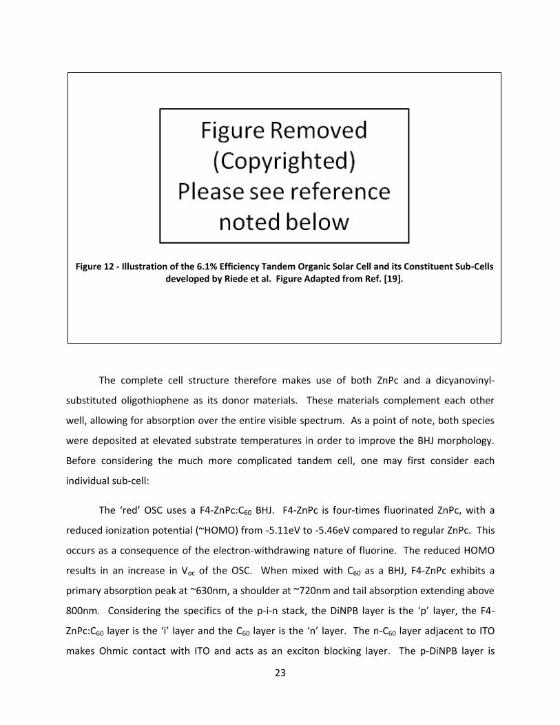
(illustrated in Figure 12, with sub-cell structures and full chemical names listed below):
- ITO/n-C60/C60/F4-ZnPc:C60 (1:1)/DiNPB/p-DiNPB/n-C60/Al (red-absorbing)
- ITO/n-C60/C60/DCV6T:C60 (2:1)/BPAPF/p-BPAPF/p-DiNPB/n-C60/Al (green-absorbing)
The following new small molecule or oligomer species were used:
- DiNPB: N,N ′ -diphenyl-N,N ′ -bis(4 ′ -(N,N-bis(naphth-1-yl)-amino)-biphenyl-4-yl)-
benzidine
- F4-ZnPc: tetra-fluoro zinc phthalocyanine
- DCV6T: α ,ω -bis-(dicyanovinylsexithiophene)-Bu(1,2,5,6) [48]
- BPAPF: 9,9-bis[4-(N,N-bis-biphenyl-4-yl-amino)phenyl]-9H-fluorene
Furthermore, ‘p-‘ and ‘n-‘ denote p- and n-doping with NDP9 AND NDP1 respectively –
materials that are proprietary from Novaled [49].
23
The complete cell structure therefore makes use of both ZnPc and a dicyanovinyl-
substituted oligothiophene as its donor materials. These materials complement each other
well, allowing for absorption over the entire visible spectrum. As a point of note, both species
were deposited at elevated substrate temperatures in order to improve the BHJ morphology.
Before considering the much more complicated tandem cell, one may first consider each
individual sub-cell:
The ‘red’ OSC uses a F4-ZnPc:C60 BHJ. F4-ZnPc is four-times fluorinated ZnPc, with a
reduced ionization potential (~HOMO) from -5.11eV to -5.46eV compared to regular ZnPc. This
occurs as a consequence of the electron-withdrawing nature of fluorine. The reduced HOMO
results in an increase in Voc of the OSC. When mixed with C60 as a BHJ, F4-ZnPc exhibits a
primary absorption peak at ~630nm, a shoulder at ~720nm and tail absorption extending above
800nm. Considering the specifics of the p-i-n stack, the DiNPB layer is the ‘p’ layer, the F4-
ZnPc:C60 layer is the ‘i’ layer and the C60 layer is the ‘n’ layer. The n-C60 layer adjacent to ITO
makes Ohmic contact with ITO and acts as an exciton blocking layer. The p-DiNPB layer is
Figure 12 - Illustration of the 6.1% Efficiency Tandem Organic Solar Cell and its Constituent Sub-Cells developed by Riede et al. Figure Adapted from Ref. [19].
24
similarly used to block excitons and to allow for easy passage of holes. The added thickness of
the p-DiNPB and n-C60 layers improves the positioning of the optical field within the devices, as
was determined by the same modelling methods described in Section 2.4.
The ‘green’ OSC uses a DCV6T donor material, where the 6 indicates 6 repeat monomer
units in the oligomer. When mixed with C60, DCV6T exhibits an absorption peak at ~570nm
with a broad shoulder extending well into the blue wavelengths. Considering the specifics of
the p-i-n stack, the BPAPF layer is the ‘p’ layer, the DCV6T:C60 layer is the ‘i’ layer and the C60
layer is the ‘n’ layer. BPAPF is chosen for the ‘p’ layer to better match the ionization potential
of DCV6T. A doped BPAPF layer is then used to reduce device series resistance and to make
contact with the p-DiNPB layer.
The tandem cell stacks the green sub-cell onto the red sub-cell, with the cells separated
by the p-DiNPB/n-C60 recombination contact. This contact has been detailed separately in [50]
for its use in tandem cell applications. It is a replacement to the previously used metal island
recombination layer described in Section 2.1. The tandem cell also makes use of a substantially
thicker p-doped DiNPB layer as an optical spacer to ensure the maxima in the optical field occur
in the i-regions of both cells. A peak efficiency is found using an optical spacer thickness of
165nm. Due to the sensitivity to optical field distribution, the authors also note that the
performance their tandem cells is strongly affected by the angle of measurement. Both Jsc and
PCE are found to drop with an increasing angle of light.
3.3.2. Highly Efficient Solar Cells Based on New Donor Materials
Steinmann et al. studied merocyanine dye MD376 as a donor in various configurations
of solar cells, including: standard BHJ solar cells, PM-HJ solar cells and the same in tandem
configurations [51]. MD376 exhibits a relatively broad absorption peak at ~610nm. For the
non-tandem devices, an optimal thickness of 50nm BHJ was used to achieve 4.3% PCE. When
incorporated into a PM-HJ, the PCE was further improved to 5%. All devices exhibited relatively
large Voc values of ~1-1.1V. The best tandem configuration device employed the following
device structure:
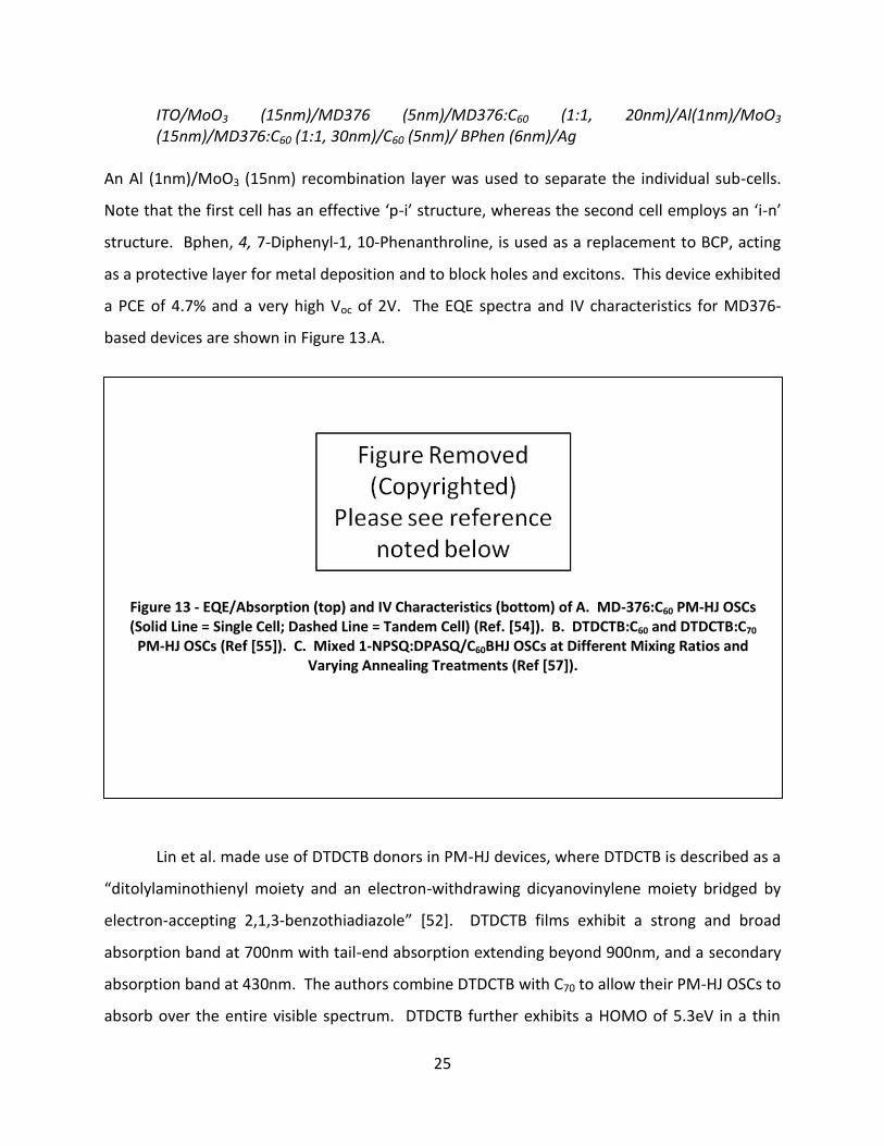
25
ITO/MoO3 (15nm)/MD376 (5nm)/MD376:C60 (1:1, 20nm)/Al(1nm)/MoO3 (15nm)/MD376:C60 (1:1, 30nm)/C60 (5nm)/ BPhen (6nm)/Ag
An Al (1nm)/MoO3 (15nm) recombination layer was used to separate the individual sub-cells.
Note that the first cell has an effective ‘p-i’ structure, whereas the second cell employs an ‘i-n’
structure. Bphen, 4, 7-Diphenyl-1, 10-Phenanthroline, is used as a replacement to BCP, acting
as a protective layer for metal deposition and to block holes and excitons. This device exhibited
a PCE of 4.7% and a very high Voc of 2V. The EQE spectra and IV characteristics for MD376-
based devices are shown in Figure 13.A.
Lin et al. made use of DTDCTB donors in PM-HJ devices, where DTDCTB is described as a
“ditolylaminothienyl moiety and an electron-withdrawing dicyanovinylene moiety bridged by
electron-accepting 2,1,3-benzothiadiazole” [52]. DTDCTB films exhibit a strong and broad
absorption band at 700nm with tail-end absorption extending beyond 900nm, and a secondary
absorption band at 430nm. The authors combine DTDCTB with C70 to allow their PM-HJ OSCs to
absorb over the entire visible spectrum. DTDCTB further exhibits a HOMO of 5.3eV in a thin
Figure 13 - EQE/Absorption (top) and IV Characteristics (bottom) of A. MD-376:C60 PM-HJ OSCs (Solid Line = Single Cell; Dashed Line = Tandem Cell) (Ref. [54]). B. DTDCTB:C60 and DTDCTB:C70
PM-HJ OSCs (Ref [55]). C. Mixed 1-NPSQ:DPASQ/C60BHJ OSCs at Different Mixing Ratios and Varying Annealing Treatments (Ref [57]).
26
film, allowing for a reasonably large Voc of 0.8V when paired with either C60 or C70. When
incorporated into a PM-HJ structure with an MoO3 hole extraction layer and a BCP exciton
blocking layer, devices were shown to be capable of 5.8% PCE. The EQE spectra and IV
characteristics for DTDCTB-based devices are shown in Figure 13.B.
Following their successes with the SQ devices detailed in Section 3.1 and 3.2, Forrest
and coworkers studied further squaraine derivatives. In particular, Wei et al. developed 2,4-
bis[4-(N-phenyl-1-naphthylamino)-2,6-dihydroxyphenyl] squaraine (1-NPSQ), a material based
on SQ, but with its isobutylamines substituted for the less bulky arylamines [53]. As a
consequence, 1-NPSQ undergoes more -stacking between donor molecules to improve hole
mobility and hole collection. In OSC performance, this is manifested as substantially reduced
series resistance and a strong improvement in fill factor. The electron-withdrawing arylamine
also serves to decrease the HOMO energy from 5.1eV to 5.3eV, thereby increasing the
theoretical Voc of the device. Finally, 1-NPSQ exhibits a slightly red-shifted absorption band
compared to SQ, with peak absorption at ~700nm and tail-end absorption to ~810nm. As with
the SQ species described in Section 3.2, thermal annealing 1-NPSQ increases both the
crystallinity and roughness of its film, allowing for increased contact area with the subsequently
deposited C60. The optimally annealed device (90oC / 10 minutes) had a PCE of 5.7%, with a Voc
of 0.9V, a FF of 64% and a Jsc of 10 mA/cm2.
Xiao et al. further improved the squaraine-based OSC efficiency by blending 1-NPSQ
with the complementary blue-shifted SQ molecule, [2-[4-( N , N -diphenylamino)-2,6-
dihydroxyphenyl]-4-diphenylamino] squaraine (DPASQ) [54]. DPASQ exhibits a peak absorption
at ~530nm. When both DPASQ and 1-NPSQ donors are used in combination with C60 acceptor
the entire visible spectrum may be captured. This is illustrated by the absorption
characteristics of these materials in Figure 13.C (top). With a HOMO of 5.4eV, the experimental
maximum Voc for DPASQ cells was found to be 1V. When employing a mixed donor layer, the
Voc generally varies in between that of 1-NPSQ and DPASQ; however, the maximum Voc of 1V
can be achieved at a mixing ratio of 1:2 1-NPSQ:DPASQ. Unfortunately, the maximum Jsc is
achieved at a mixing ratio of 2:1 1-NPSQ:DPASQ. The addition of DPASQ helps improve the EQE
27
from 500-600nm; however, increasing the concentration of DPASQ beyond 50% substantially
decreases the contribution from 1-NPSQ in the 600-700nm region, thus deteriorating the Jsc.
In order to further improve the cell performance, solvent annealing with DCM was
performed, and a 1,4,5,8-napthalene-tetracarboxylic-dianhydride (NTCDA) / PTCBI optical
spacer was added between the C60 and Al layers. Addition of the optical spacer resulted in an
increase in short circuit current, which followed from the fact that the peak electric field
intensity better overlapped with the active layers. Solvent annealing further increased the
short circuit current and improved the FF to a very high value of 72%, but decreased the Voc
from 1V to 0.8V. In spite of the decreased Voc, this optimized, solvent-annealed OSC exhibited
an impressive PCE of 5.9%. The IV characteristics for the various iterations of these devices are
shown in Figure 13.C (bottom).
4. Conclusions
Organic electronics, and OPVs in particular, are a rapidly developing and constantly
evolving field. While soluble organic materials, including polymers and soluble small molecules,
offer substantial cost benefits due to their potential ease of fabrication, they typically exhibit
poor reproducibility. The high number of experimental variables makes these systems
inherently difficult to study. As such, in order to obtain a fundamental understanding of the
efficiency limitations and degradation mechanisms of OSCs, the insoluble and vacuum-
deposited small molecules are of particular interest. The most basic OSC architectures formed
by thermally evaporated small molecules are the PHJ, BHJ, tandem PHJ and tandem BHJ OSCs.
The BHJ cells may be further refined into p-i-n solar cells, where the ‘i’ layer is the BHJ. A
common subset of the p-i-n solar cell, denoted as the PM-HJ, simply borders the ‘i’-layer with
pure donor and acceptor layers for the ‘p’ and ‘n’ layers respectively. In all of these systems,
with a strong emphasis on tandem OSCs, the distribution of the electric field within the device
layers has been identified as a significant factor to limit the PCE. In order to address these
concerns, researchers have adapted transfer matrix formalism to identify the position of the
peak electric field in any OSC.
28
The focus of OPVs has shifted from the realization of new device architectures to the
creation of new donor materials and to the optimization of the current systems by clever
fabrication techniques. With regard to the first point, research groups have studied a wide
range of different materials with varying degrees of success. The most successful alternative
donor materials in literature include F4-ZnPc, DCV6T, DTDCTB, MD376 merocyanine dye and
squaraine derivatives, allowing for PCEs ranging from 5% to 6.1%. These materials were all
designed specifically for their broad absorption bands, as well as their relatively deep HOMO
levels for enhanced Voc values.
Device optimization and refinement has focused on the addition of inter-layers for
enhanced electrical properties, light absorption or material crystallization. Several groups have
successfully increased the absorption range of their OSCs by the insertion of a thin secondary
donor layer immediately prior to the deposition of their primary donor BHJ. Meanwhile, other
researchers have investigated improved morphology by additional or modified deposition
techniques. Some methods are simple, such as strong annealing treatments to create an
interdigitated network of donor and acceptor materials, while others involve substantial
deviations from regular fabrication – such as WEG, or the deposition of stacks comprised of
alternating ultra-thin (1-2nm) layers of donor and acceptor.
New materials development and further device optimization techniques, such as those
detailed in this review, should eventually allow for 15% PCE OSCs. Unfortunately, there are still
a number of hurdles that must be surpassed before OSCs are a viable commercial product.
With meagre device lifetimes, the degradation study of OSCs is still a very young field that
requires massive research efforts. Further, most OSCs to date have been fabricated as lab-scale
devices with device areas typically less than 1cm2. Scaling up these devices and integrating
them into panels will prove to be difficult, especially with the commonly high OSC series
resistances. Regardless, with OSC efficiencies already above 10% and Heliatek quoting device
harvesting factors 15-25% higher than crystalline silicon and other thin-film solar technologies,
it is clear that OPVs are quickly becoming a strong competitor in the solar industry.
References [1] M. T. Lloyd, et al., "Photovoltaics from soluble small molecules," Materials Today, vol.
10, pp. 34-41, Nov 2007. [2] J. Roncali, "Molecular Bulk Heterojunctions: An Emerging Approach to Organic Solar
Cells," Accounts of chemical research, vol. 42, pp. 1719-1730, Nov 2009. [3] B. Walker, et al., "Small Molecule Solution-Processed Bulk Heterojunction Solar Cells,"
Chemistry of Materials, 2011. [4] A. Mishra and P. Bäuerle, "Small Molecule Organic Semiconductors on the Move:
Promises for Future Solar Energy Technology," Angewandte Chemie International Edition, vol. 51, pp. 2020-2067, 2012.
[5] Y. M. Sun, et al., "Solution-processed small-molecule solar cells with 6.7% efficiency," Nature Materials, vol. 11, pp. 44-48, Jan 2012.
[6] M. T. Dang, et al., "P3HT: PCBM, Best Seller in Polymer Photovoltaic Research," Advanced Materials, 2011.
[7] E. Bundgaard and F. C. Krebs, "Low band gap polymers for organic photovoltaics," Solar Energy Materials and Solar Cells, vol. 91, pp. 954-985, Jul 2007.
[8] C. J. Brabec, et al., "Polymer-Fullerene Bulk-Heterojunction Solar Cells," Advanced Materials, vol. 22, pp. 3839-3856, Sep 2010.
[9] N. Blouin, et al., "Toward a rational design of poly(2,7-carbazole) derivatives for solar cells," Journal of the American Chemical Society, vol. 130, pp. 732-742, Jan 2008.
[10] G. Dennler, et al., "Design Rules for Donors in Bulk-Heterojunction Tandem Solar Cells? Towards 15% Energy-Conversion Efficiency," Advanced Materials, vol. 20, pp. 579-583, 2008.
[11] J. Chen and Y. Cao, "Development of novel conjugated donor polymers for high-efficiency bulk-heterojunction photovoltaic devices," Accounts of chemical research, vol. 42, pp. 1709-1718, 2009.
[12] Y. J. Cheng, et al., "Synthesis of conjugated polymers for organic solar cell applications," Chemical reviews, vol. 109, pp. 5868-5923, 2009.
[13] Mitsubishi Chemical. (2011, Accessed: June 15, 2012). Progress Report 1: Solution-Processable Organic Photovoltaic (OPV) Modules. Available: http://www.m-kagaku.co.jp/english/aboutmcc/RC/special/index.html
[14] Heliatek. (April 27, 2012, Accessed: June 15, 2012). HeliaTek Sets New World Record Efficiency of 10.7% for its Organic Solar Cell. Available: http://www.heliatek.com/?p=1923&lang=en
[15] C. Tang, "Two layer organic photovoltaic cell," Applied Physics Letters, vol. 48, pp. 183-185, 1986.
[16] P. Peumans, et al., "Small molecular weight organic thin-film photodetectors and solar cells," Journal of Applied Physics, vol. 93, p. 3693, 2003.
[17] A. Yakimov and S. R. Forrest, "High photovoltage multiple-heterojunction organic solar cells incorporating interfacial metallic nanoclusters," Applied Physics Letters, vol. 80, pp. 1667-1669, Mar 2002.
[18] D. Gebeyehu, et al., "Bulk-heterojunction photovoltaic devices based on donor-acceptor organic small molecule blends," Solar Energy Materials and Solar Cells, vol. 79, pp. 81-92, Aug 2003.
[19] M. Riede, et al., "Efficient Organic Tandem Solar Cells based on Small Molecules," Advanced Functional Materials, vol. 21, pp. 3019-3028, Aug 2011.
[20] J. Drechsel, et al., "MIP-type organic solar cells incorporating phthalocyanine/fullerene mixed layers and doped wide-gap transport layers," Organic Electronics, vol. 5, pp. 175-186, Jun 2004.
[21] S. Uchida, et al., "Organic small molecule solar cells with a homogeneously mixed copper phthalocyanine: C-60 active layer," Applied Physics Letters, vol. 84, pp. 4218-4220, May 2004.
[22] J. Xue, et al., "Mixed donor-acceptor molecular heterojunctions for photovoltaic applications. II. Device performance," Journal of Applied Physics, vol. 98, p. 124903, 2005.
[23] J. G. Xue, et al., "A hybrid planar-mixed molecular heterojunction photovoltaic cell," Advanced Materials, vol. 17, pp. 66-+, Jan 2005.
[24] B. Maennig, et al., "Organic p-i-n solar cells," Applied Physics a-Materials Science & Processing, vol. 79, pp. 1-14, Jun 2004.
[25] J. Drechsel, et al., "Efficient organic solar cells based on a double p-i-n architecture using doped wide-gap transport layers," Applied Physics Letters, vol. 86, Jun 2005.
[26] J. G. Xue, et al., "Asymmetric tandem organic photovoltaic cells with hybrid planar-mixed molecular heterojunctions," Applied Physics Letters, vol. 85, pp. 5757-5759, Dec 2004.
[27] J. Y. Kim, et al., "Efficient tandem polymer solar cells fabricated by all-solution processing," Science, vol. 317, pp. 222-225, 2007.
[28] A. P. Yuen, et al., "Photovoltaic properties of M-phthalocyanine/fullerene organic solar cells," Solar Energy, 2012.
[29] W. Wang, et al., "Planar and textured heterojunction organic photovoltaics based on chloroindium phthalocyanine (ClInPc) versus titanyl phthalocyanine (TiOPc) donor layers," Organic Electronics, vol. 12, pp. 383-393, 2011.
[30] N. M. Bamsey, et al., "Heteromorphic chloroindium phthalocyanine films for improved photovoltaic performance," Solar Energy Materials and Solar Cells, 2011.
[31] D. Fujishima, et al., "Organic thin-film solar cell employing a novel electron-donor material," Solar Energy Materials and Solar Cells, vol. 93, pp. 1029-1032, 2009.
[32] S. Y. Wang, et al., "High efficiency organic photovoltaic cells based on a vapor deposited squaraine donor," Applied Physics Letters, vol. 94, Jun 2009.
[33] A. Cravino, et al., "Light-emitting organic solar cells based on a 3D conjugated system with internal charge transfer," Advanced Materials, vol. 18, pp. 3033-+, Nov 2006.
[34] H. Kageyama, et al., "High-Performance Organic Photovoltaic Devices Using a New Amorphous Molecular Material with High Hole Drift Mobility, Tris 4-(5-phenylthiophen-2-yl)phenyl amine," Advanced Functional Materials, vol. 19, pp. 3948-3955, Dec 2009.
[35] S. Roquet, et al., "Triphenylamine-thienylenevinylene hybrid systems with internal charge transfer as donor materials for heterojunction solar cells," Journal of the American Chemical Society, vol. 128, pp. 3459-3466, Mar 2006.
[36] M. Lloyd, et al., "Photovoltaic cells from a soluble pentacene derivative," Organic Electronics, vol. 7, pp. 243-248, 2006.
[37] P. F. Xia, et al., "Triarylamino and Tricyanovinyl End-Capped Oligothiophenes with Reduced Optical Gap for Photovoltaic Applications," Journal of Physical Chemistry C, vol. 112, pp. 16714-16720, Oct 2008.
[38] P. F. Xia, et al., "Donor-Acceptor Oligothiophenes as Low Optical Gap Chromophores for Photovoltaic Applications," Advanced Materials, vol. 20, pp. 4810-+, Dec 2008.
[39] A. P. Yuen, et al., "A simple parallel tandem organic solar cell based on metallophthalocyanines," Applied Physics Letters, vol. 98, p. 173301, 2011.
[40] H. L. Wong, et al., "Efficient photovoltaic cells with wide photosensitization range fabricated from rhenium benzathiazole complexes," Applied Physics Letters, vol. 90, Feb 2007.
[41] I. Kim, et al., "Enhanced power conversion efficiency of p-i-n type organic solar cells by employing a p-layer of palladium phthalocyanine," Applied Physics Letters, vol. 97, Nov 2010.
[42] I. Kim, et al., "Enhancement of device performance of organic solar cells by an interfacial perylene derivative layer," Acs Applied Materials & Interfaces, vol. 2, pp. 1390-1394, May 2010.
[43] M. Hirade and C. Adachi, "Small molecular organic photovoltaic cells with exciton blocking layer at anode interface for improved device performance," Applied Physics Letters, vol. 99, Oct 2011.
[44] J. Sakai, et al., "Pentacene:Fullerene Multilayer-Heterojunction Organic Photovoltaic Cells Fabricated by Alternating Evaporation Method," Japanese Journal of Applied Physics, vol. 49, 2010.
[45] F. Yang, et al., "Efficient Solar Cells Using All‐Organic Nanocrystalline Networks," Advanced Materials, vol. 19, pp. 4166-4171, 2007.
[46] G. D. Wei, et al., "Efficient, Ordered Bulk Heterojunction Nanocrystalline Solar Cells by Annealing of Ultrathin Squaraine Thin Films," Nano Letters, vol. 10, pp. 3555-3559, Sep 2010.
[47] B. Yu, et al., "Efficient Organic Solar Cells Using a High-Quality Crystalline Thin Film as a Donor Layer," Advanced Materials, vol. 22, pp. 1017-+, Mar 2010.
[48] R. Fitzner, et al., "Dicyanovinyl–Substituted Oligothiophenes: Structure‐Property Relationships and Application in Vacuum‐Processed Small Molecule Organic Solar Cells," Advanced Functional Materials, 2011.
[49] Novaled. (2012, Accessed: July 20, 2012). Organic Material for Organic Photovoltaic. Available: http://www.novaled.com/products/organic_material/for_organic_photovoltaic/
[50] R. Timmreck, et al., "Highly doped layers as efficient electron-hole recombination contacts for tandem organic solar cells," Journal of Applied Physics, vol. 108, Aug 2010.
[51] V. Steinmann, et al., "A simple merocyanine tandem solar cell with extraordinarily high open-circuit voltage," Applied Physics Letters, vol. 99, Nov 2011.
[52] L. Y. Lin, et al., "A Low-Energy-Gap Organic Dye for High-Performance Small-Molecule Organic Solar Cells," Journal of the American Chemical Society, vol. 133, pp. 15822-15825, Oct 2011.
[53] G. D. Wei, et al., "Arylamine-Based Squaraine Donors for Use in Organic Solar Cells," Nano Letters, vol. 11, pp. 4261-4264, Oct 2011.
[54] X. Xiao, et al., "Small‐Molecule Photovoltaics Based on Functionalized Squaraine Donor Blends," Advanced Materials, 2012.
[55] L. A. A. Pettersson, et al., "Modeling photocurrent action spectra of photovoltaic devices based on organic thin films," Journal of Applied Physics, vol. 86, p. 487, 1999.
[56] D. W. Sievers, et al., "Modeling optical effects and thickness dependent current in polymer bulk-heterojunction solar cells," Journal of Applied Physics, vol. 100, p. 114509, 2006.
[57] Z. Liu, et al., "The characterization of the optical functions of BCP and CBP thin films by spectroscopic ellipsometry," Synthetic Metals, vol. 150, pp. 159-163, 2005.
[58] A. Djurisic, et al., "Optical properties of copper phthalocyanine," Optics communications, vol. 205, pp. 155-162, 2002.
[59] H. Hoppe, et al., "Optical constants of conjugated polymer/fullerene based bulk-heterojunction organic solar cells," Molecular Crystals and Liquid Crystals, vol. 385, pp. 113-119, 2002.
[60] G. Dennler, et al., "Angle dependence of external and internal quantum efficiencies in bulk-heterojunction organic solar cells," Journal of Applied Physics, vol. 102, pp. 054516-054516-7, 2007.
[61] Z. Liu, et al., "The optical functions of metal phthalocyanines," Journal of Physics D: Applied Physics, vol. 37, p. 678, 2004.
i
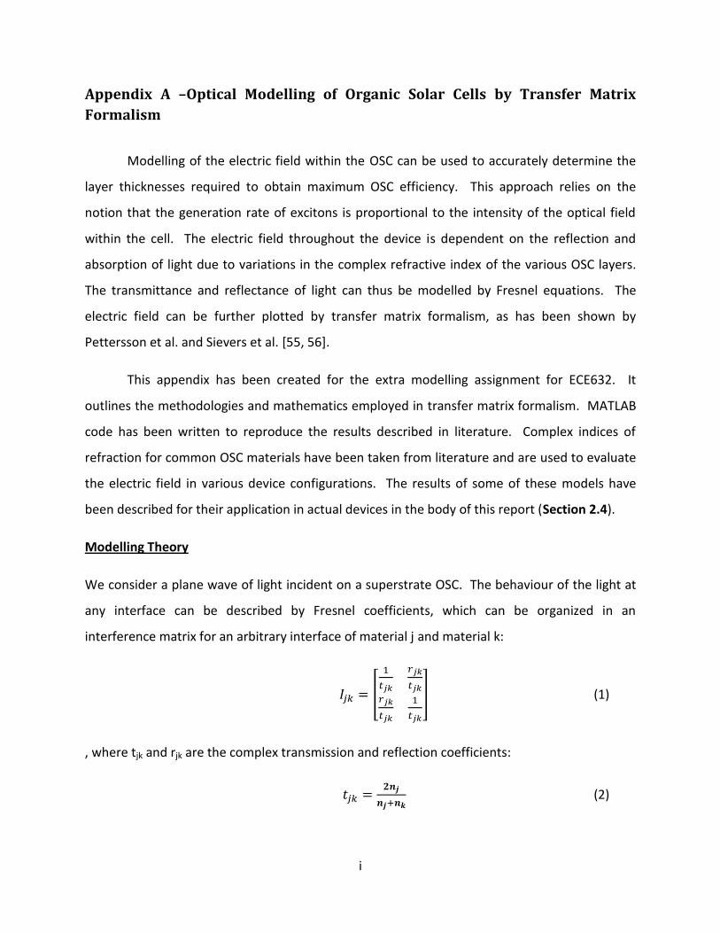
Appendix A –Optical Modelling of Organic Solar Cells by Transfer Matrix
Formalism
Modelling of the electric field within the OSC can be used to accurately determine the
layer thicknesses required to obtain maximum OSC efficiency. This approach relies on the
notion that the generation rate of excitons is proportional to the intensity of the optical field
within the cell. The electric field throughout the device is dependent on the reflection and
absorption of light due to variations in the complex refractive index of the various OSC layers.
The transmittance and reflectance of light can thus be modelled by Fresnel equations. The
electric field can be further plotted by transfer matrix formalism, as has been shown by
Pettersson et al. and Sievers et al. [55, 56].
This appendix has been created for the extra modelling assignment for ECE632. It
outlines the methodologies and mathematics employed in transfer matrix formalism. MATLAB
code has been written to reproduce the results described in literature. Complex indices of
refraction for common OSC materials have been taken from literature and are used to evaluate
the electric field in various device configurations. The results of some of these models have
been described for their application in actual devices in the body of this report (Section 2.4).
Modelling Theory
We consider a plane wave of light incident on a superstrate OSC. The behaviour of the light at
any interface can be described by Fresnel coefficients, which can be organized in an
interference matrix for an arbitrary interface of material j and material k:
(1)
, where tjk and rjk are the complex transmission and reflection coefficients:
(2)
ii
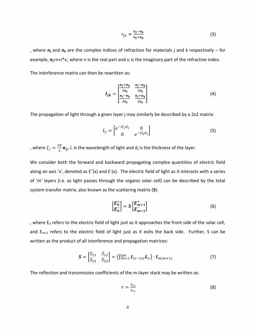
(3)
, where nj and nk are the complex indices of refraction for materials j and k respectively – for
example, nj=n+i*, where n is the real part and is the imaginary part of the refractive index.
The interference matrix can then be rewritten as:
(4)
The propagation of light through a given layer j may similarly be described by a 2x2 matrix:
(5)
, where
, is the wavelength of light and dj is the thickness of the layer.
We consider both the forward and backward propagating complex quantities of electric field
along an axis ‘x’, denoted as E+(x) and E-(x). The electric field of light as it interacts with a series
of ‘m’ layers (i.e. as light passes through the organic solar cell) can be described by the total
system transfer matrix, also known as the scattering matrix (S):
(6)
, where E0 refers to the electric field of light just as it approaches the front side of the solar cell,
and Em+1 refers to the electric field of light just as it exits the back side. Further, S can be
written as the product of all interference and propagation matrices:
(7)
The reflection and transmission coefficients of the m-layer stack may be written as:
(8)

iii
(9)
Since the glass substrate is generally quite thick, it is cumbersome and impractical to include it
in the transfer-matrix calculation. Following the approach by [56], the intensity of the light
after it has passed through the substrate can instead be calculated as:
(10)
, where I0 is the intensity of the incident plane wave, Ts is the transmittance of the substrate, Rs
is the reflectance of the substrate, s is the absorption coefficient of the substrate, ds is the
thickness of the substrate and R is the reflectance of the remaining layers of the OSC.
The reflectance of the remaining layers of the OSC can be found as:
(11)
The intensity of the input light varies with wavelength and is defined by the AM1.5 1-sun solar
spectrum.
Using Is, the incident electric field, after passage through the substrate, can be found as:
(12)
For the purposes of this model, ES effectively refers to E0+ in equation (6) above.
In order to calculate the electric field at a specific distance x within layer j, it is necessary to
break apart the total system transfer matrix into partial transfer matrices. One may define
S=Sj’LjSj’’, where Sj’ is the partial transfer matrix prior to layer j, Sj’’ is the partial transfer matrix
after layer j, and Lj is the propagation matrix for layer j, as defined in equation (5) above. Sj’
and Sj’’ may be written as:
(13)
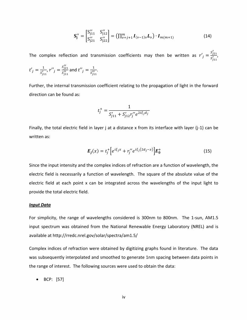
iv
(14)
The complex reflection and transmission coefficients may then be written as
,
,
and
.
Further, the internal transmission coefficient relating to the propagation of light in the forward
direction can be found as:
Finally, the total electric field in layer j at a distance x from its interface with layer (j-1) can be
written as:
(15)
Since the input intensity and the complex indices of refraction are a function of wavelength, the
electric field is necessarily a function of wavelength. The square of the absolute value of the
electric field at each point x can be integrated across the wavelengths of the input light to
provide the total electric field.
Input Data
For simplicity, the range of wavelengths considered is 300nm to 800nm. The 1-sun, AM1.5
input spectrum was obtained from the National Renewable Energy Laboratory (NREL) and is
available at http://rredc.nrel.gov/solar/spectra/am1.5/
Complex indices of refraction were obtained by digitizing graphs found in literature. The data
was subsequently interpolated and smoothed to generate 1nm spacing between data points in
the range of interest. The following sources were used to obtain the data:
BCP: [57]

v
CuPc: [58]
C60: [55]
glass: [59]
ITO: [59]
PEDOT:PSS: [59]
P3HT:PCBM (1:1) BHJ: [60]
ZnPc: [61]
ZnPc:C60 (1:1) BHJ: [24]
Metal complex indices of refraction were obtained from http://refractiveindex.info/
Printouts of the complex indices of refraction are available upon request.
MATLAB Implementation and Output
In order to demonstrate the basic implementation of this model, the following P3HT:PCBM BHJ
device is modelled:
Layer 0: Glass, thickness = 0.7mm
Layer 1: ITO, thickness = 100nm
Layer 2: PEDOT:PSS, thickness = 30nm
Layer 3: P3HT:PCBM (1:1), thickness = 70nm & 200nm
Layer 4: Aluminum, thickness = 100nm
Layer 5: Air
All thicknesses are representative of a realistic device structure capable of producing 2-3% PCE
in a laboratory device. 70nm P3HT:PCBM would be fabricated by spincoating from a
chlorobenzene solvent. 200nm P3HT:PCBM would be fabricated by spinning at higher weight
percents from a dichlorobenzene solvent.
The code used for this model is available at the end of this document. The output figures are
shown below in Figure A.1 with the various layers labelled.
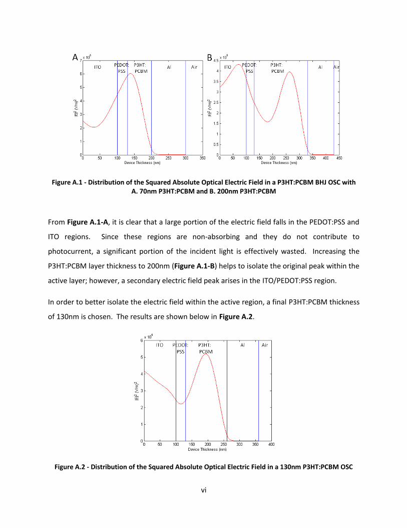
vi
Figure A.1 - Distribution of the Squared Absolute Optical Electric Field in a P3HT:PCBM BHJ OSC with A. 70nm P3HT:PCBM and B. 200nm P3HT:PCBM
From Figure A.1-A, it is clear that a large portion of the electric field falls in the PEDOT:PSS and
ITO regions. Since these regions are non-absorbing and they do not contribute to
photocurrent, a significant portion of the incident light is effectively wasted. Increasing the
P3HT:PCBM layer thickness to 200nm (Figure A.1-B) helps to isolate the original peak within the
active layer; however, a secondary electric field peak arises in the ITO/PEDOT:PSS region.
In order to better isolate the electric field within the active region, a final P3HT:PCBM thickness
of 130nm is chosen. The results are shown below in Figure A.2.
Figure A.2 - Distribution of the Squared Absolute Optical Electric Field in a 130nm P3HT:PCBM OSC
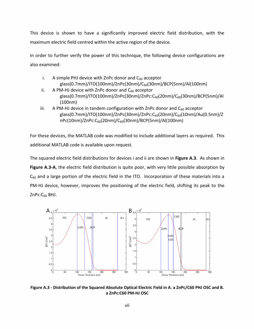
vii
This device is shown to have a significantly improved electric field distribution, with the
maximum electric field centred within the active region of the device.
In order to further verify the power of this technique, the following device configurations are
also examined:
i. A simple PHJ device with ZnPc donor and C60 acceptor glass(0.7mm)/ITO(100nm)/ZnPc(30nm)/C60(30nm)/BCP(5nm)/Al(100nm)
ii. A PM-HJ device with ZnPc donor and C60 acceptor glass(0.7mm)/ITO(100nm)/ZnPc(30nm)/ZnPc:C60(20nm)/C60(30nm)/BCP(5nm)/Al(100nm)
iii. A PM-HJ device in tandem configuration with ZnPc donor and C60 acceptor glass(0.7mm)/ITO(100nm)/ZnPc(30nm)/ZnPc:C60(20nm)/C60(10nm)/Au(0.5nm)/ZnPc(10nm)/ZnPc:C60(20nm)/C60(30nm)/BCP(5nm)/Al(100nm)
For these devices, the MATLAB code was modified to include additional layers as required. This
additional MATLAB code is available upon request.
The squared electric field distributions for devices i and ii are shown in Figure A.3. As shown in
Figure A.3-A, the electric field distribution is quite poor, with very little possible absorption by
C60 and a large portion of the electric field in the ITO. Incorporation of these materials into a
PM-HJ device, however, improves the positioning of the electric field, shifting its peak to the
ZnPc:C60 BHJ.
Figure A.3 - Distribution of the Squared Absolute Optical Electric Field in A. a ZnPc/C60 PHJ OSC and B. a ZnPc:C60 PM-HJ OSC
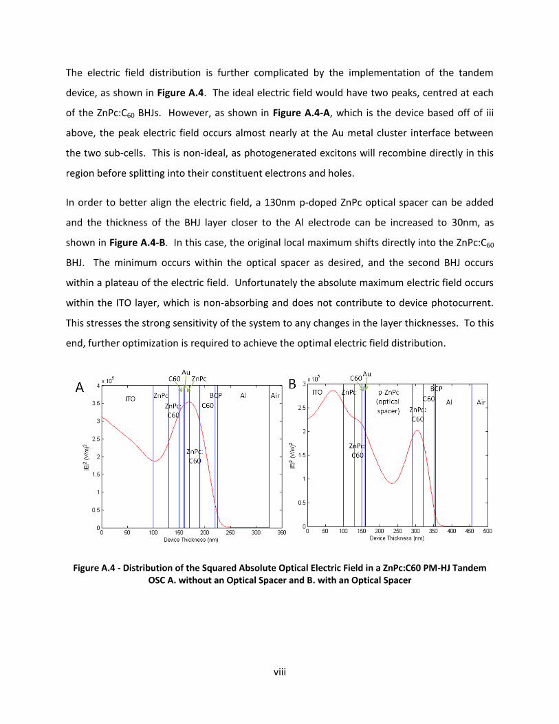
viii
The electric field distribution is further complicated by the implementation of the tandem
device, as shown in Figure A.4. The ideal electric field would have two peaks, centred at each
of the ZnPc:C60 BHJs. However, as shown in Figure A.4-A, which is the device based off of iii
above, the peak electric field occurs almost nearly at the Au metal cluster interface between
the two sub-cells. This is non-ideal, as photogenerated excitons will recombine directly in this
region before splitting into their constituent electrons and holes.
In order to better align the electric field, a 130nm p-doped ZnPc optical spacer can be added
and the thickness of the BHJ layer closer to the Al electrode can be increased to 30nm, as
shown in Figure A.4-B. In this case, the original local maximum shifts directly into the ZnPc:C60
BHJ. The minimum occurs within the optical spacer as desired, and the second BHJ occurs
within a plateau of the electric field. Unfortunately the absolute maximum electric field occurs
within the ITO layer, which is non-absorbing and does not contribute to device photocurrent.
This stresses the strong sensitivity of the system to any changes in the layer thicknesses. To this
end, further optimization is required to achieve the optimal electric field distribution.
Figure A.4 - Distribution of the Squared Absolute Optical Electric Field in a ZnPc:C60 PM-HJ Tandem OSC A. without an Optical Spacer and B. with an Optical Spacer
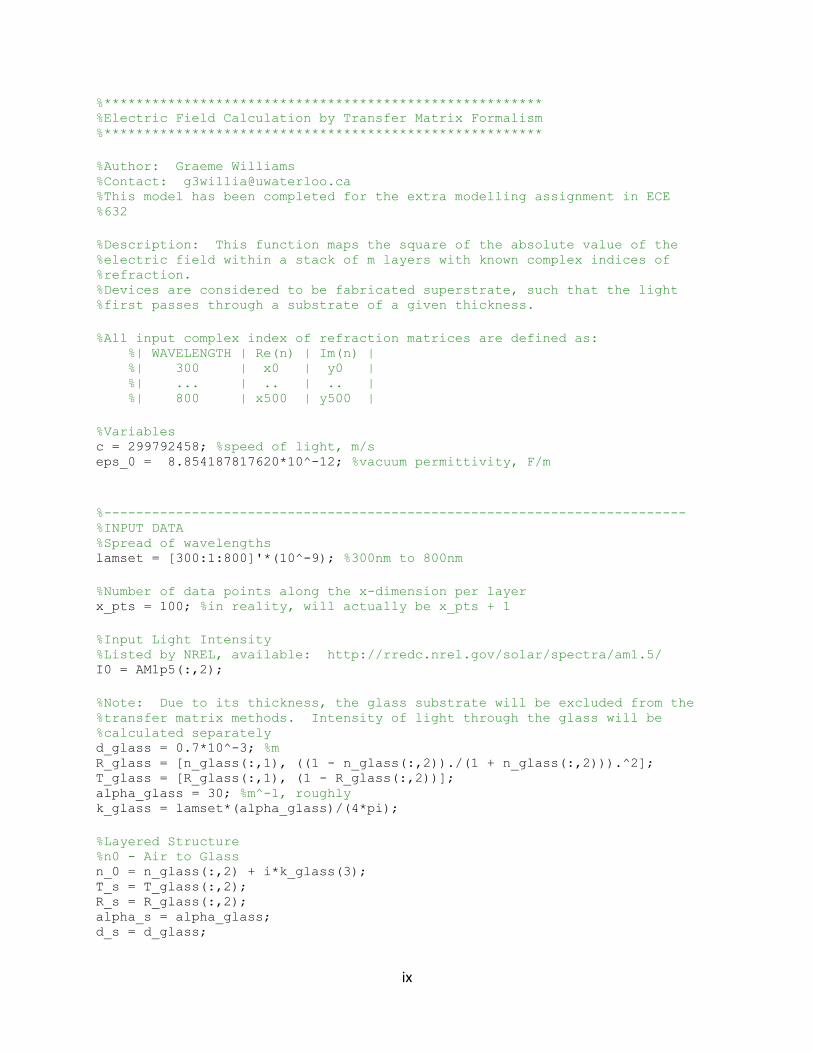
ix
%******************************************************* %Electric Field Calculation by Transfer Matrix Formalism %*******************************************************
%Author: Graeme Williams %Contact: [email protected] %This model has been completed for the extra modelling assignment in ECE %632
%Description: This function maps the square of the absolute value of the %electric field within a stack of m layers with known complex indices of %refraction. %Devices are considered to be fabricated superstrate, such that the light %first passes through a substrate of a given thickness.
%All input complex index of refraction matrices are defined as: %| WAVELENGTH | Re(n) | Im(n) | %| 300 | x0 | y0 | %| ... | .. | .. | %| 800 | x500 | y500 |
%Variables c = 299792458; %speed of light, m/s eps_0 = 8.854187817620*10^-12; %vacuum permittivity, F/m
%------------------------------------------------------------------------- %INPUT DATA %Spread of wavelengths lamset = [300:1:800]'*(10^-9); %300nm to 800nm
%Number of data points along the x-dimension per layer x_pts = 100; %in reality, will actually be x_pts + 1
%Input Light Intensity %Listed by NREL, available: http://rredc.nrel.gov/solar/spectra/am1.5/ I0 = AM1p5(:,2);
%Note: Due to its thickness, the glass substrate will be excluded from the %transfer matrix methods. Intensity of light through the glass will be %calculated separately d_glass = 0.7*10^-3; %m R_glass = [n_glass(:,1), ((1 - n_glass(:,2))./(1 + n_glass(:,2))).^2]; T_glass = [R_glass(:,1), (1 - R_glass(:,2))]; alpha_glass = 30; %m^-1, roughly k_glass = lamset*(alpha_glass)/(4*pi);
%Layered Structure %n0 - Air to Glass n_0 = n_glass(:,2) + i*k_glass(3); T_s = T_glass(:,2); R_s = R_glass(:,2); alpha_s = alpha_glass; d_s = d_glass;
x
%1 - ITO n_1 = n_ITO(:,2) + i*n_ITO(:,3); xi_1 = (2*pi*n_1)./lamset; alpha_1 = n_ITO(:,3)*(4*pi)./lamset; d_1 = 100*10^-9; %100nm, in m %2 - PEDOT:PSS n_2 = n_pedot(:,2) + i*n_pedot(:,3); xi_2 = (2*pi*n_2)./lamset; alpha_2 = n_pedot(:,3)*(4*pi)./lamset; d_2 = 30*10^-9; %30nm, in m %3 - P3HT:PCBM n_3 = n_p3pc(:,2) + i*n_p3pc(:,3); xi_3 = (2*pi*n_3)./lamset; alpha_3 = n_p3pc(:,3)*(4*pi)./lamset; d_3 = 70*10^-9; %70nm, in m %4 - Al n_4 = n_Al(:,2) + i*n_Al(:,3); xi_4 = (2*pi*n_4)./lamset; alpha_4 = n_Al(:,3)*(4*pi)./lamset; d_4 = 100*10^-9; %100nm, in m %5 - Air (assume vacuum for simplicity) n_5 = zeros(501,1); %-------------------------------------------------------------------------
%------------------------------------------------------------------------- %Calculation of overall reflection and transmission coefficients %& Definition of parameters for subsequent analysis
%Initializing variables for later use R = []; T = []; t1_plus = []; r1_pp = []; t2_plus = []; r2_pp = []; t3_plus = []; r3_pp = []; t4_plus = []; r4_pp = [];
%Looping through the wavelengths 300nm to 800nm for j=1:501 %*** Across n0 to n1 %Interface Matrix I_01 = [ ( (n_0(j) + n_1(j))/(2*n_0(j)) ), ( (n_0(j) - ... n_1(j))/(2*n_0(j)) ); ( (n_0(j) - n_1(j))/(2*n_0(j)) ), ... ( (n_0(j) + n_1(j))/(2*n_0(j)) )];
%*** Through n1 %Layer Matrix L_1 = [exp(-i*(xi_1(j)*d_1)), 0; 0, exp(i*(xi_1(j)*d_1))];
%*** Across n1 to n2 %Interface Matrix I_12 = [ ( (n_1(j) + n_2(j))/(2*n_1(j)) ), ( (n_1(j) - ... n_2(j))/(2*n_1(j)) ); ( (n_1(j) - n_2(j))/(2*n_1(j)) ), ...
xi
( (n_1(j) + n_2(j))/(2*n_1(j)) )];
%*** Through n2 %Layer Matrix L_2 = [exp(-i*(xi_2(j)*d_2)), 0; 0, exp(i*(xi_2(j)*d_2))];
%*** Across n2 to n3 %Interface Matrix I_23 = [ ( (n_2(j) + n_3(j))/(2*n_2(j)) ), ( (n_2(j) - ... n_3(j))/(2*n_2(j)) ); ( (n_2(j) - n_3(j))/(2*n_2(j)) ), ... ( (n_2(j) + n_3(j))/(2*n_2(j)) )];
%*** Through n3 %Layer Matrix L_3 = [exp(-i*(xi_3(j)*d_3)), 0; 0, exp(i*(xi_3(j)*d_3))];
%*** Across n3 to n4 %Interface Matrix I_34 = [ ( (n_3(j) + n_4(j))/(2*n_3(j)) ), ( (n_3(j) - ... n_4(j))/(2*n_3(j)) ); ( (n_3(j) - n_4(j))/(2*n_3(j)) ), ... ( (n_3(j) + n_4(j))/(2*n_3(j)) )];
%Through n4 %Layer Matrix L_4 = [exp(-i*(xi_4(j)*d_4)), 0; 0, exp(i*(xi_4(j)*d_4))];
%*** Across n4 to n5 %Interface Matrix I_45 = [ ( (n_4(j) + n_5(j))/(2*n_4(j)) ), ( (n_4(j) - ... n_5(j))/(2*n_4(j)) ); ( (n_4(j) - n_5(j))/(2*n_4(j)) ), ... ( (n_4(j) + n_5(j))/(2*n_4(j)) )];
%Calculating the total transfer matrix for this lambda S = I_01*L_1*I_12*L_2*I_23*L_3*I_34*L_4*I_45;
%Calculating the total reflectance and transmittance parameters r = S(2,1)/S(1,1); t = 1/S(1,1);
%Calculating the parameters wrt power/intensity R = [R; abs(r^2)];
%********************************************************************** %Calculating partial transfer matrices (for position-dependent %intensity calculations - see below) S1_p = I_01; S1_pp = I_12*L_2*I_23*L_3*I_34*L_4*I_45; S2_p = I_01*L_1*I_12; S2_pp = I_23*L_3*I_34*L_4*I_45; S3_p = I_01*L_1*I_12*L_2*I_23; S3_pp = I_34*L_4*I_45; S4_p = I_01*L_1*I_12*L_2*I_23*L_3*I_34; S4_pp = I_45;
%Calculating relevant transmission and reflection parameters
xii
r1_pp = [r1_pp; S1_pp(2,1)/S1_pp(1,1)]; r2_pp = [r2_pp; S2_pp(2,1)/S2_pp(1,1)]; r3_pp = [r3_pp; S3_pp(2,1)/S3_pp(1,1)]; r4_pp = [r4_pp; S4_pp(2,1)/S4_pp(1,1)];
t1_plus = [t1_plus; (S1_p(1,1) + S1_p(1,2)*r1_pp(j)*... exp(2*i*xi_1(j)*d_1))^(-1)]; t2_plus = [t2_plus; (S2_p(1,1) + S2_p(1,2)*r2_pp(j)*... exp(2*i*xi_2(j)*d_2))^(-1)]; t3_plus = [t3_plus; (S3_p(1,1) + S3_p(1,2)*r3_pp(j)*... exp(2*i*xi_3(j)*d_3))^(-1)]; t4_plus = [t4_plus; (S4_p(1,1) + S4_p(1,2)*r4_pp(j)*... exp(2*i*xi_4(j)*d_4))^(-1)];
end %-------------------------------------------------------------------------
%------------------------------------------------------------------------- %Calculation of the internal transmittance through the glass substrate T_int = (T_s.*exp(-alpha_s.*d_s))./(1-(R.*R_s.*exp(-2.*alpha_s.*d_s))); %-------------------------------------------------------------------------
%------------------------------------------------------------------------- %Calculation of position-dependent reflection and transmission coefficients
%Defining the inital electric field intensity based on: %I=(c*n*eps0/2)*abs(E)^2 E0 = sqrt(2*(I0.*T_int)./(c*n_glass(:,2)*eps_0));
%Initializing variables for later use E1 = []; E2 = []; E3 = [];
%Layer 0 (substrate) Is = I0.*T_int;
%Layer 1-3 %Splitting layers into finite segments %Layer 1 delta_d1 = d_1 / x_pts; d1_pts = [0:delta_d1:d_1]; %Layer 2 delta_d2 = d_2 / x_pts; d2_pts = [0:delta_d2:d_2]; %Layer 3 delta_d3 = d_3 / x_pts; d3_pts = [0:delta_d3:d_3]; %Layer 4 delta_d4 = d_4 / x_pts; d4_pts = [0:delta_d4:d_4];
%Looping through the wavelengths for j=1:501
xiii
for k=1:(x_pts+1) E1(j,k) = E0(j) * t1_plus(j)*(exp(i*xi_1(j)*d1_pts(k)) + ... r1_pp(j)*exp(i*xi_1(j)*(2*d_1-d1_pts(k)))); E2(j,k) = E0(j) * t2_plus(j)*(exp(i*xi_2(j)*d2_pts(k)) + ... r2_pp(j)*exp(i*xi_2(j)*(2*d_2-d2_pts(k)))); E3(j,k) = E0(j) * t3_plus(j)*(exp(i*xi_3(j)*d3_pts(k)) + ... r3_pp(j)*exp(i*xi_3(j)*(2*d_3-d3_pts(k)))); E4(j,k) = E0(j) * t4_plus(j)*(exp(i*xi_4(j)*d4_pts(k)) + ... r4_pp(j)*exp(i*xi_4(j)*(2*d_4-d4_pts(k)))); end end
%Integrating intensity across the visible spectrum Esq1 = abs(E1).^2; Esq2 = abs(E2).^2; Esq3 = abs(E3).^2; Esq4 = abs(E4).^2;
xvals = AM1p5(:,1); Esq1sum = []; Esq2sum = []; Esq3sum = []; Esq4sum = [];
for k=1:(x_pts+1) y1vals = Esq1(:,k); y2vals = Esq2(:,k); y3vals = Esq3(:,k); y4vals = Esq4(:,k);
Esq1sum = [Esq1sum, trapz(xvals,y1vals)]; Esq2sum = [Esq2sum, trapz(xvals,y2vals)]; Esq3sum = [Esq3sum, trapz(xvals,y3vals)]; Esq4sum = [Esq4sum, trapz(xvals,y4vals)]; end
%Plotting the output data total_y = [Esq1sum Esq2sum Esq3sum Esq4sum]; x1max = max(d1_pts); x2max = max(d2_pts) + x1max; x3max = max(d3_pts) + x2max; x4max = max(d4_pts) + x3max; total_x = [d1_pts (x1max + d2_pts) (x2max + d3_pts) (x3max + d4_pts)]; p1 = plot(total_x,total_y, 'red'); p1_axis = axis;
%Drawing vertical lines to visually separate layers hold on line([x1max x1max], [0 p1_axis(4)]) line([x2max x2max], [0 p1_axis(4)]) line([x3max x3max], [0 p1_axis(4)]) line([x4max x4max], [0 p1_axis(4)])