Embed Size (px)
Citation preview
Hindawi Publishing CorporationAdvances in OptoElectronicsVolume 2007, Article ID 40285, 15 pagesdoi:10.1155/2007/40285
Review ArticleRecent Advances in Organic Solar Cells
Thomas Kietzke
Institute of Materials Research and Engineering (IMRE), 3 Research Link, Singapore 117602
Received 24 May 2007; Accepted 16 August 2007
Recommended by A. G. Aberle
Solar cells based on organic semiconductors have attracted much attention. The thickness of the active layer of organic solar cells istypically only 100 nm thin, which is about 1000 times thinner than for crystalline silicon solar cells and still 10 times thinner thanfor current inorganic thin film cells. The low material consumption per area and the easy processing of organic semiconductorsoffer a huge potential for low cost large area solar cells. However, to compete with inorganic solar cells the efficiency of organicsolar cells has to be improved by a factor of 2-3. Several organic semiconducting materials have been investigated so far, but theoptimum material still has to be designed. Similar as for organic light emitting devices (OLED) small molecules are competingwith polymers to become the material of choice. After a general introduction into the device structures and operational principlesof organic solar cells the three different basic types (all polymer based, all small molecules based and small molecules mixed withpolymers) are described in detail in this review. For each kind the current state of research is described and the best of class reportedefficiencies are listed.
Copyright © 2007 Thomas Kietzke. This is an open access article distributed under the Creative Commons Attribution License,which permits unrestricted use, distribution, and reproduction in any medium, provided the original work is properly cited.
1. INTRODUCTION
Organic photovoltaic devices have gained a broad interest inthe last few years due to their potential for large-area low-cost solar cells. From the first reports on molecular thinfilm devices more than 30 years ago, their power conver-sion efficiencies have increased considerably from 0.001% in1975 [1] to 1% in 1986 [2] and more recently to 5.5% in2006 [3–6]. The progresses in efficiency will possibly makethem a competitive alternative to inorganic solar cells in thenear future. Different concepts have been published using ei-ther small molecules [1–4, 7], conjugated polymers [7–17],combinations of small molecules and conjugated polymers[18–20], or combinations of inorganic and organic mate-rials [21] as the active layer. “Active layer” refers here tothe layer in which the majority of the incident light is ab-sorbed and charges are generated. Small molecules and poly-mers differ in their molecular weights. Commonly, macro-molecules with a molecular weight larger than 10 000 amuare called polymers, whereas lighter molecules are referred toas “oligomers” or “small molecules.”
Historically, small molecules were mainly deposited byvacuum deposition techniques since they showed limitedsolubility in common solvents. In contrast to these smallmolecule thin films, the preparation of thin polymer lay-ers does not require high vacuum sublimation steps. Large
polymer thin film areas can be deposited by several methods,such as spin-coating, screen printing, spray coating, or ink jetprinting, allowing for large-area, ultrathin, flexible, and low-cost devices. Currently, there is a head-to-head race going onbetween solution processed and sublimed organic solar cells,but the ease of processability may finally tip the balance infavour of polymers or small molecules blended with poly-mers. Although it should be noted that currently there aresome efforts to develop soluble oligomers to allow for costefficient solution processing techniques, the concept of effi-cient complete small molecules-based devices prepared fromsolution processing has yet to be proven.
2. DEVICE STRUCTURE AND OPERATION
Organic semiconductors differ from classical crystalline in-organic semiconductors (e.g., silicon) in many fundamentalaspects.
First of all, the mobilities of organic semiconductors areseveral orders of magnitude less than those found in crys-talline inorganic semiconductors [22]. Transport processesin organic semiconductors are best described by hoppingtransport in contrast to the band transport in most crys-talline inorganic semiconductors. Even the highest reportedhole mobilities (μh) for organic semiconductors reach cur-rently only about 15 cm2V−1s−1 for single crystals of small

2 Advances in OptoElectronics
Charge transfer
LUMO
HOMO
Donor Acceptor
φVac
Δφ
(a)
Energy transfer
LUMO
HOMO
Donor Acceptor
φVac
Δφ
(b)
Figure 1: The interface between two different semiconducting polymers (D = donor, A = acceptor) can facilitate either charge transfer bysplitting the exciton or energy transfer, where the whole exciton is transferred from the donor to the acceptor.
molecules [23] and 0.6 cm2V−1s−1 for liquid crystalline poly-mers [24] (silicon: μh = 450 cm2V−1s−1). Highest elec-tron mobilities (μe) for organic materials are typically lower,hovering around 0.1 cm2V−1s−1 reaching higher values onlyin particular TFT structures using highly crystalline smallmolecules [25, 26] (silicon: μe = 1400 cm2V−1s−1). The mo-bility values for amorphous organic materials as used mostcommonly in organic solar cells are even several magnitudeslower. These low mobilities limit the feasible thicknesses ofthe organic layer in solar cells to a few hundred nanome-tres. Fortunately, organic semiconductors are very strong ab-sorbers in the UV-VIS regime. Thus only ca. 100 nm thickorganic layers are needed for effective absorption.
Second, the exciton binding energy in organic semicon-ductors is much higher than, for example, in silicon. Uponabsorption of a photon of sufficient energy by the organicsemiconductor, an electron is promoted into the lowest un-occupied molecular orbital (LUMO), leaving behind a holein the highest occupied molecular orbital (HOMO). How-ever, due to electrostatic interactions, this electron-hole pairforms a tightly bound state which is called singlet exciton.The exact binding energy of this exciton is still under de-bate but it is expected to be in a range of 200–500 meV[27, 28]. Hence, the exciton binding energy for organic semi-conductors is roughly one order of magnitude larger thanfor inorganic semiconductors like silicon, where photoexci-tations typically lead directly to free carriers at room temper-ature. The thermal energy at room temperature (∼25 meV)is not sufficient to efficiently generate free charge carriersin organic materials by exciton dissociation, even at typi-cal internal electric fields (∼106–107 V/m) [29]. For example,in the widely used Poly(2-methoxy-5-(2′-ethyl-hexyloxy)-p-phenylene vinylene) (MEH-PPV) [30] experiments revealedthat only 10% of the excitons dissociate into free carriers in apure layer [31], while the remaining excitons decay via radia-tive or nonradiative recombination pathways. Thus, the en-ergy efficiencies of single-layer polymer devices remain typi-cally below 0.1% [27, 32].
The most important discovery on the route to high-efficiency organic solar cells was the finding that solar cellscontaining a heterojunction between hole and electron ac-cepting organic materials exhibited performances far supe-rior to single component devices [2, 8–10]. Using the het-
erojunction approach, photogenerated excitons (bound elec-tron-hole pairs) in the polymer layer can be efficiently dis-sociated into free carriers at the interface, whereas in singlecomponent devices most excitons recombine after a shorttime. The charge separation occurs at the interface betweendonor and acceptor molecules, mediated by a large potentialdrop. After photo-excitation of an electron from the HOMOto the LUMO, the electron can jump from the LUMO of thedonor (the material with the higher LUMO) to the LUMO ofthe acceptor if the potential difference ΔΦbetween the ion-isation potential of the donor and the electron affinity ofthe acceptor is larger than the exciton binding energy (seeFigure 1). However, this process, which is called photoin-duced charge transfer, can lead to free charges only if thehole remains on the donor due to its higher HOMO level.In contrast, if the HOMO of the acceptor is higher, the exci-ton transfers itself completely to the material of lower-bandgap accompanied by energy loss.
For efficient exciton dissociation at the heterojunction,the donor and acceptor materials have to be in close proxim-ity. The optimum length scale is in the range of the excitondiffusion length, typically a few tens of nanometres. On theother hand, the thickness of the active layer should be com-parable to the penetration length of the incident light, whichfor organic semiconductors is typically 80–200 nm.
A heterojunction can be realised in several ways (seeFigure 2). The most straightforward approach is the prepa-ration of a bilayer by subliming or by spin-coating a secondlayer on top of the first, resulting in a more or less diffusedbilayer structure [11, 33, 34]. If polymers are used and bothmaterials are soluble in the same solvents, laminating tech-niques can be used [10, 35]. This bilayer geometry guaranteesdirectional photoinduced charge transfer across the inter-face. Since both types of charge carriers travel to their respec-tive electrodes in pure n-type or p-type layers, the chances forrecombination losses are significantly reduced. However, theinterfacial area and thus the exciton dissociation efficiencyare limited. Higher interfacial areas and thus improved ex-citon dissociation efficiencies can be achieved if layers con-taining both the electron donor and electron acceptor in amixture are prepared. These so-called bulk heterojunctionscan be deposited either by cosublimation of small moleculesor by spin-coating mixtures of polymers.

Thomas Kietzke 3
Bi-layer heterojunction
CathodeAcceptor
Donor
ITO
Substrate
Light
100 nm
Direct path for charge carriers toelectrodes
(a)
Bulk heterojunction
Cathode
D/A blend
ITO
Substrate
Light
100 nm
Large interfacial area due to phase separationin the blend, but percolation needed
(b)
Figure 2: Two approaches to heterojunction solar cells.
Recombination
An
ode
Cat
hod
e
Phot
on
Photon
Photon
GenerationDiffusion
Drift/diffusion
Charge separation ElectronHole
Exciton
+ + + +− − − −
−+ −+ −+−+
Donor Acceptor
+− +−
Figure 3: Principle of charge separation in a solar cell.
The drawback of the bulk heterojunction structure is thata percolating pathway for the hole and electron transportingphase to the electrodes is needed in order that the separatedcharge carriers can reach their corresponding electrodes.
If the individual layer thicknesses (in case of a bilayerstructure) or the phase separated domains (in case of a blendlayer) is larger than the exciton diffusion length, then mostexcitons will recombine (Figure 3). If, however, the excitonsare generated in close proximity to an interface, they have achance to be separated into free charge carriers which maydiffuse or drift to the corresponding electrodes. The overallefficiency of this process is described by the incident pho-ton to converted electron efficiency (IPCE). The IPCE is cal-culated by the number of electrons leaving the device undershort circuit condition per time and area divided by the num-ber of photons incident per time and area:
IPCE = # extracted electrons# incident photons
. (1)
Note that the IPCE is a measure of the external quantum ef-ficiency, meaning that losses due to reflection at the surfaceor transmission through the device are included in the IPCEvalue. Subtracting these two loss channels would lead to theinternal quantum efficiency, which is, however, rarely used tocompare solar cells.
Solar cells are further characterised by measuring thecurrent-voltage I(V) curve under illumination of a lightsource that mimics the sun spectrum. A typical current-voltage I(V) curve of a polymer solar cell is shown inFigure 4. Since organic semiconductors show very low intrin-sic carrier concentration, the metal-insulator-metal (MIM)[36] model seems to be best suited to explain this character-istic. The characteristic points used to characterise a solar cellare labelled in Figure 4. In addition, for each of these points,the energy diagram for a single-layer cell with an indium tinoxide (ITO) anode and aluminium cathode is displayed.
(a) The current delivered by a solar cell under zero biasis called short circuit current (Isc). In this case, ex-citon dissociation and charge transport is driven bythe so-called built-in potential. In the MIM picture,this potential is equal to the difference in work func-tion (Wf) of the hole- and electron-collecting elec-trodes. For polymer solar cells, the transparent ITOelectrode is often chosen (Wf,ITO = 4.7 eV) in com-bination with a low work function material (Wf,Ca =2.87 eV, Wf,Mg = 3.66 eV, Wf,Al = 4.24 eV) [37] ascounter-electrode to achieve a high internal field [38–41]. For example, the difference in work functions be-tween ITO and Ca is approximately 2 eV.
(b) The voltage where the current equals zero is calledopen circuit voltage (Voc). In the MIM picture this sit-uation is described by the case where the band is flat,since the applied voltage equals the difference in thework function of the electrodes. (Note that diffusioneffects are neglected in this simplified picture.)
(c) When V > Voc, the diode is biased in the forward di-rection. Electrons are now injected from the low work

4 Advances in OptoElectronics
0.2
0
−0.2
Isc
−0.4
Cu
rren
t(A
)
−1 0 1 Voc 2
Voltage (V)
Pmax
a
b
c
d
(a)
a) b)
c) d)
ITO
ITO
ITO
ITOCathode
Cathode
Cathode
Cathode
+Voc−
+ −− +
(b)
Figure 4: Current (voltage) characteristics of a typical organicdiode shown together with the metal-insulator-metal (MIM) pic-ture for the characteristic points. (a) Short circuit condition. (b)Open circuit condition. (c) Forward bias. (d) Reverse bias.
function electrode into the LUMO and holes from thehigh work function electrode into the HOMO of theorganic layer, respectively.
(d) When V < 0, the diode is driven under a reverse bi-ased condition the solar cells works as a photodiode.The field is higher than in (a) which often leads to en-hanced charge generation and/or collection efficiency.
The point where the electrical power P = I × V reachesthe maximum value represents the condition where the so-lar cell can deliver its maximum power to an external load. Itis called the maximum power point. The ratio of this maxi-mum electrical power Pmax to the product of the short circuitcurrent and the open circuit voltage is termed the fill factor(FF):
FF = Pmax
Isc ×Voc. (2)
Ideally, the fill factor should be unity, but losses due to trans-port and recombination result in values between 0.2–0.7 for
organic photovoltaic devices. As an example, a constant slopeof the I(V) characteristic corresponds to FF = 0.25.
The photovoltaic power conversion efficiency (η) is thencalculated for an incident light power Plight:
η = Isc ×Voc × FFPlight
. (3)
3. SMALL MOLECULE-BASED SOLAR CELLS
The first efforts to fabricate organic photovoltaic devices us-ing small molecules date back to 1975, however efficienciesdid not reach more than 0.001% at that time. The work ofTang [2] in 1986 is commonly cited as the groundbreak-ing discovery that sparked the current interest in the field.Using copper phthalocyanine (CuPc) as the electron donorand a perylene derivative, 3,4,9,10-perylene tetracarboxylicbis-benzimidazole (confusingly referred to as PTCBI, PV, orPBI), as the electron acceptor in a simple bilayer structure,a power conversion efficiency of 1% was reported. The opencircuit voltage reached 450 mV and the fill factor of 65% indi-cated excellent charge transport. For the past 20 years, CuPchas been the donor of choice in most small molecule solarcells due to its high stability, high mobility, and widespreadavailability. The device physics of small molecule solar cellsis described in a review paper of Peumans et al. [42]. Theoriginal Tang structure was improved by cosublimation ofCuPc and PTCBI leading to a blend structure followed by anannealing step [43]. Due to the improved interfacial area, ahigher efficiency (η = 1.5%) was obtained. Later in 2005,a novel deposition method called vapour phase deposition(VPE) helped to increase the efficiency for this system furthersince a highly intermixed donor-acceptor interface could beobtained [44, 45]. The interfacial area was increased by a fac-tor of four compared to a bilayer structure while still main-taining n-type and p-type percolating pathways, and a powerconversion efficiency of 2.2% was reported [44, 45].
Although C60 (fullerene) does not show strong absorp-tion properties in the visible region, its much larger ex-citon diffusion length compared to PTCBI is favorable toachieve higher efficiencies. Devices based on incorporatingCuPc:C60 bulk heterojunctions reached power conversionefficiencies of up to 5% [3, 6, 46]. The highest efficiency foran organic solar cell so far was reached by Xue et al. [4] for astacked solar cell comprising two CuPc:C60 bulk heterojunc-tion cells separated via a layer of silver nanoclustors, whichserved as a charge recombination layer.
The drawback of using CuPc as an electron donor isthat only relative small open circuit voltages (<0.6 V) canbe reached with perylenes or fullerenes as acceptors, sincea large portion of photon energy is wasted when the photo-generated electron on CuPc transfers to C60 or perylene. Theopen circuit voltage could be increased by using boron sub-phthalocyanine (SubPc) instead of CuPc [47]. The HOMOlevel of SubPc (HOMO:−5.6 eV) is shifted by approximately400 meV compared to CuPc (HOMO: −5.2 eV). As a re-sult, the Voc increased by the same amount to nearly 1 V.The SubPc:C60 device reached a power conversion efficiencyof 2.1% leaving room for further improvement. If CuPc is

Thomas Kietzke 5
N N N
N N N
CuN N
CuPc
(a)
C60
(b)
NC
CN
CN
CN
S
S
Bu Bu Bu Bu
S
S
S
DCV5T
(c)
O
N
NO
N
N
PTCBI
(d)
Figure 5: Chemical structures of most important small molecules used for organic solar cells.
substituted by tin(II) phtalocyanine (SnPc), the photore-sponse increases from 800 nm to nearly 1000 nm [48]. How-ever, the hole mobility in SnPc is very low limiting the devicepower conversion efficiency to around 1%.
A promising alternative to CuPc or phtalocyanines ingeneral was presented by Schulze et al. [49] using α,α-bis(2,2-dicyanovinyl)-quinquwthiophene (DCV5T) as elec-tron donor in combination with C60 (see Figure 5 for thechemical structure). Since the HOMO level of DCV5T is suf-ficiently low (−5.6 eV), open circuit voltages of 1 V could beobtained. The IPCE reached values as high as 52% leadingto a high overall efficiency of 3.4%. In another approach,a glass forming thienylenevinylenetriphenylanylamine [50]was used in combination with C60 for devices with open cir-cuit voltages as high as 1.15 V. However, the power conver-sion efficiency was limited to 1.9% by its small fill factor.
An overview of small molecules solar cells can be foundin Table 1.
4. POLYMER-BASED SOLAR CELLS
4.1. Introduction
For most of their history, polymers have been considered aselectrical insulators. It was the discovery in 1977 by the groupof Heeger, Shirakawa, and MacDiarmid that doped poly-acetylene could achieve metallic conductivity which initiatedintense research on conjugated polymers [53]. The work ofthese three pioneers was later honoured with the Nobel Prizein Chemistry in 2000 [54–56]. From this earlier work, it wasnot till the late 1990s that highly purified and soluble con-jugated polymers became widely available. While initial re-search was concentrated mostly on improving the conduc-tivity of conjugated polymers by chemical doping, serious
interest also grew in intrinsically semiconducting and highlysoluble polymers. From then on, the application of conju-gated polymers for a wide range of semiconductor devicessuch as light emitting diodes (LEDs) [30, 57], solar cells, andthin film transistors (TFTs) [58] was systematically investi-gated.
The conjugated systems of these polymers usually con-sist of chains and rings of carbon atoms in sp1 and sp2 hy-bridisation, leading to a framework of alternating double- ortriple- and single-bonds. In this representation, single bondsare σ-bonds, and double bonds contain a σ-bond and a π-bond. However, in reality, the π-electrons are not constrictedto the individual bonds, but rather are delocalised over theentire molecule. Thus conjugated polymers can be regardedas quasi one-dimensional semiconductors. The extent of theπ-orbital overlap together with the bond alternation definesthe band gap.
Layers containing a mixture of an electron donating andan electron accepting polymer (so-called polymer blends)can be prepared by spin-coating from a solution containingboth polymers in the same solvent [8, 13, 14]. Since the en-tropy of mixing is generally low for polymers, solid polymerblends tend to phase-separate, leading to a distributed bulkheterojunction. A large donor-acceptor interface is formedwithout any additional processing steps. If donor and accep-tor components are intimately mixed such that the lengthscale of the phase separation is in the range of the excitondiffusion length (<10 nm), nearly all excitons can be sepa-rated. Moreover, when a thin layer of immiscible polymers isdeposited from solution, the resulting morphology stronglydepends on various parameters such as the individual solu-bility of the polymers in the solvent, the interaction with thesubstrate surface, the layer thickness, the deposition method,and the drying process [59–65]. Therefore, the adjustment
6 Advances in OptoElectronics
Table 1: Best in class solar cells: small molecule-based solar cells.
Donor Acceptor η Voc FF IPCE Reference
CuPc C60 5.7% 1.0 V 59% NA Xue et al. [4]
CuPc C60 5.0% 0.6 V 60% 64% Xue et al. [6]
MeO-TPD, ZnPc (stacked) C60 3.8% 1.0 V 47% NA Drechsel et al. [51]
CuPc C60 3.5% 0.5 V 46% NA Uchida et al. [46]
DCV5T C60 3.4% 1.0 V 49% 52% Schulze et al. [49]
CuPc PTCBI 2.7% 0.5 V 58% NA Yang et al. [44, 45]
SubPc C60 2.1% 1.0 V 57% NA Mutolo et al. [47]
MeO-TPD, ZnPc C60 2.1% 0.5 V 37% NA Drechsel et al. [51]
TDCV-TPA C60 1.9% 1.2 V 28% NA Cravino et al. [50]
Pentacene on PET C60 1.6% 0.3 V 48% 30% Pandey and Nunzi [52]
SnPc C60 1.0% 0.4 V 50% 21% Rand et al. [48]
(a) (b)
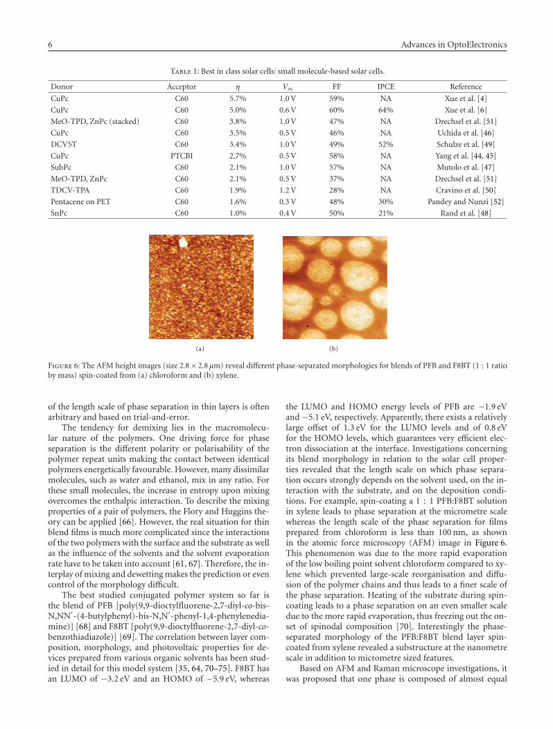
Figure 6: The AFM height images (size 2.8× 2.8 μm) reveal different phase-separated morphologies for blends of PFB and F8BT (1 : 1 ratioby mass) spin-coated from (a) chloroform and (b) xylene.
of the length scale of phase separation in thin layers is oftenarbitrary and based on trial-and-error.
The tendency for demixing lies in the macromolecu-lar nature of the polymers. One driving force for phaseseparation is the different polarity or polarisability of thepolymer repeat units making the contact between identicalpolymers energetically favourable. However, many dissimilarmolecules, such as water and ethanol, mix in any ratio. Forthese small molecules, the increase in entropy upon mixingovercomes the enthalpic interaction. To describe the mixingproperties of a pair of polymers, the Flory and Huggins the-ory can be applied [66]. However, the real situation for thinblend films is much more complicated since the interactionsof the two polymers with the surface and the substrate as wellas the influence of the solvents and the solvent evaporationrate have to be taken into account [61, 67]. Therefore, the in-terplay of mixing and dewetting makes the prediction or evencontrol of the morphology difficult.
The best studied conjugated polymer system so far isthe blend of PFB [poly(9,9-dioctylfluorene-2,7-diyl-co-bis-N,NN′-(4-butylphenyl)-bis-N,N′-phenyl-1,4-phenylenedia-mine)] [68] and F8BT [poly(9,9-dioctylfluorene-2,7-diyl-co-benzothiadiazole)] [69]. The correlation between layer com-position, morphology, and photovoltaic properties for de-vices prepared from various organic solvents has been stud-ied in detail for this model system [35, 64, 70–75]. F8BT hasan LUMO of −3.2 eV and an HOMO of −5.9 eV, whereas
the LUMO and HOMO energy levels of PFB are −1.9 eVand −5.1 eV, respectively. Apparently, there exists a relativelylarge offset of 1.3 eV for the LUMO levels and of 0.8 eVfor the HOMO levels, which guarantees very efficient elec-tron dissociation at the interface. Investigations concerningits blend morphology in relation to the solar cell proper-ties revealed that the length scale on which phase separa-tion occurs strongly depends on the solvent used, on the in-teraction with the substrate, and on the deposition condi-tions. For example, spin-coating a 1 : 1 PFB:F8BT solutionin xylene leads to phase separation at the micrometre scalewhereas the length scale of the phase separation for filmsprepared from chloroform is less than 100 nm, as shownin the atomic force microscopy (AFM) image in Figure 6.This phenomenon was due to the more rapid evaporationof the low boiling point solvent chloroform compared to xy-lene which prevented large-scale reorganisation and diffu-sion of the polymer chains and thus leads to a finer scale ofthe phase separation. Heating of the substrate during spin-coating leads to a phase separation on an even smaller scaledue to the more rapid evaporation, thus freezing out the on-set of spinodal composition [70]. Interestingly the phase-separated morphology of the PFB:F8BT blend layer spin-coated from xylene revealed a substructure at the nanometrescale in addition to micrometre sized features.
Based on AFM and Raman microscope investigations, itwas proposed that one phase is composed of almost equal
Thomas Kietzke 7
F8BT-rich
PFB-rich
5 μm
(a)
F8BT-rich PFB-rich
1 μm
(b)
F8BT-rich
PFB-rich
200 μm
(c)
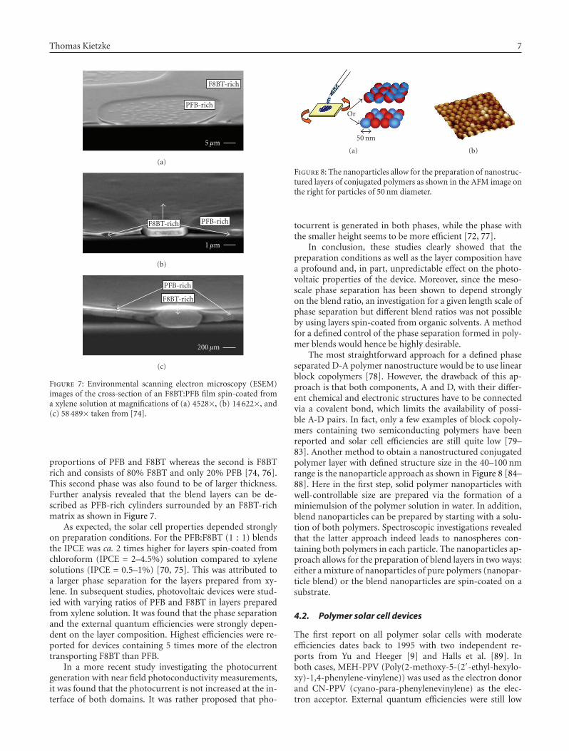
Figure 7: Environmental scanning electron microscopy (ESEM)images of the cross-section of an F8BT:PFB film spin-coated froma xylene solution at magnifications of (a) 4528×, (b) 14 622×, and(c) 58 489× taken from [74].
proportions of PFB and F8BT whereas the second is F8BTrich and consists of 80% F8BT and only 20% PFB [74, 76].This second phase was also found to be of larger thickness.Further analysis revealed that the blend layers can be de-scribed as PFB-rich cylinders surrounded by an F8BT-richmatrix as shown in Figure 7.
As expected, the solar cell properties depended stronglyon preparation conditions. For the PFB:F8BT (1 : 1) blendsthe IPCE was ca. 2 times higher for layers spin-coated fromchloroform (IPCE = 2–4.5%) solution compared to xylenesolutions (IPCE = 0.5–1%) [70, 75]. This was attributed toa larger phase separation for the layers prepared from xy-lene. In subsequent studies, photovoltaic devices were stud-ied with varying ratios of PFB and F8BT in layers preparedfrom xylene solution. It was found that the phase separationand the external quantum efficiencies were strongly depen-dent on the layer composition. Highest efficiencies were re-ported for devices containing 5 times more of the electrontransporting F8BT than PFB.
In a more recent study investigating the photocurrentgeneration with near field photoconductivity measurements,it was found that the photocurrent is not increased at the in-terface of both domains. It was rather proposed that pho-
Or
50 nm
(a) (b)
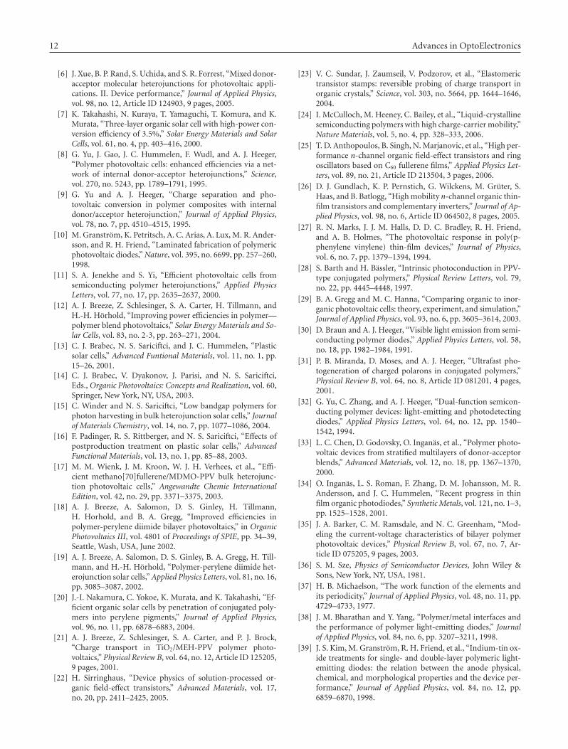
Figure 8: The nanoparticles allow for the preparation of nanostruc-tured layers of conjugated polymers as shown in the AFM image onthe right for particles of 50 nm diameter.
tocurrent is generated in both phases, while the phase withthe smaller height seems to be more efficient [72, 77].
In conclusion, these studies clearly showed that thepreparation conditions as well as the layer composition havea profound and, in part, unpredictable effect on the photo-voltaic properties of the device. Moreover, since the meso-scale phase separation has been shown to depend stronglyon the blend ratio, an investigation for a given length scale ofphase separation but different blend ratios was not possibleby using layers spin-coated from organic solvents. A methodfor a defined control of the phase separation formed in poly-mer blends would hence be highly desirable.
The most straightforward approach for a defined phaseseparated D-A polymer nanostructure would be to use linearblock copolymers [78]. However, the drawback of this ap-proach is that both components, A and D, with their differ-ent chemical and electronic structures have to be connectedvia a covalent bond, which limits the availability of possi-ble A-D pairs. In fact, only a few examples of block copoly-mers containing two semiconducting polymers have beenreported and solar cell efficiencies are still quite low [79–83]. Another method to obtain a nanostructured conjugatedpolymer layer with defined structure size in the 40–100 nmrange is the nanoparticle approach as shown in Figure 8 [84–88]. Here in the first step, solid polymer nanoparticles withwell-controllable size are prepared via the formation of aminiemulsion of the polymer solution in water. In addition,blend nanoparticles can be prepared by starting with a solu-tion of both polymers. Spectroscopic investigations revealedthat the latter approach indeed leads to nanospheres con-taining both polymers in each particle. The nanoparticles ap-proach allows for the preparation of blend layers in two ways:either a mixture of nanoparticles of pure polymers (nanopar-ticle blend) or the blend nanoparticles are spin-coated on asubstrate.
4.2. Polymer solar cell devices
The first report on all polymer solar cells with moderateefficiencies dates back to 1995 with two independent re-ports from Yu and Heeger [9] and Halls et al. [89]. Inboth cases, MEH-PPV (Poly(2-methoxy-5-(2′-ethyl-hexylo-xy)-1,4-phenylene-vinylene)) was used as the electron donorand CN-PPV (cyano-para-phenylenevinylene) as the elec-tron acceptor. External quantum efficiencies were still low

8 Advances in OptoElectronics
O
CH3O
OCH3
CH CH
CH3O
CH CHn
M3EH-PPV
∗ ∗N Nn
PFB
H HS n
P3HT
Electron donors
∗
∗O
O n
MDMO-PPV
(a)
O
CN
C CH
OC8H17
C8H17O
CH C
CNn
CN-ether-PPV
∗ ∗
SN N
n
F8BT
∗
∗S
CN
H21C10O
OCH3
CN
S
C8H17 C8H17
n
PF1CVTP
Electron acceptors
(b)
Figure 9: Chemical structures of conjugated polymers used in organic solar cells.
(around 5-6%), most likely due to the nanomorphology notbeing optimized. A big efficiency jump was obtained afterthe CN-PPV was modified by introduction of an ether groupto increase solubility [90]. Using the copolymer M3EH-PPV(see Figure 9 for the chemical structures) as donor and CN-Ether-PPV as acceptor, Breeze et al. [91] demonstrated in2000 external quantum efficiencies of 24% correspondingto 0.6% power conversion efficiency. Even higher efficien-cies were published by the same authors in 2004 [12]. Inthat work, it was demonstrated for the first time that 1%power conversion efficiency could be reached in a polymer-polymer blend device. The open circuit voltage was 1 V, how-ever the low fill factor of 25% left room for further improve-ment. The highest power conversion efficiency so far for so-lar cells composed of polymer blend was reached in 2005by Kietzke et al. [92] using the same materials coupled withimproved processing. It could be shown that annealing thelayer leads to an improvement of the efficiency by a fac-tor of two compared to the prepared layers [93]. An opencircuit voltage of 1.36 V and a white light conversion effi-ciency of 1.7% were obtained. The fill factor reached 35%indicating improved charge transport. Photophysical stud-ies on PPV-based blends revealed that the exciplex forma-tion in this system might have been a major loss factor [92–94].
Recently Koetse et al. [95] reported solar cells basedon MDMO-PPV as donor and a novel acceptor copolymer
PF1CVTP. A high quantum efficiency of 42% was achieved.However, the power conversion efficiency could not set a newrecord, since the conversion efficiency decreased at higherlight intensities typical for solar illumination.
Several approaches have also been investigated for poly-mer bilayer structures. Alam and Jenekhe [96] reported de-vices based on insoluble PPV as donor and BBL as elec-tron acceptor. BBL was deposited from methanesulfonic acid.The devices showed extremely high quantum efficiencies ofup to 62%. Unfortunately, the device efficiency decreased athigher light intensities dramatically. The power conversionefficiency dropped from record breaking 5% at very low lightintensities to 1.5% under standard 1 sun. Similar efficienciescould be reached for M3EH-PPV as donor and CN-Ether-PPV as acceptor.
Polymer solar cells have much room for optimization(the characteristic parameters of the best of their kind arein Tables 2 and 3). Both the fill factor and the quantum effi-ciency need to be doubled in order to reach 6-7% power con-version efficiency. Recent experiments indicated that the de-vice performance is currently limited largely by the low dis-sociation efficiency of the photogenerated excitons into freecharge carriers. Even after dissociation, the electrons tendto localise near the heterointerface in the electron accept-ing polymers due to their amorphous nature. To proceed tohigher efficiencies more crystalline electron acceptor poly-mers with larger electron mobilities are needed [93].

Thomas Kietzke 9
Table 2: Best in class solar cells: polymer-polymer (blend) solar cells.
Donor Acceptor η Voc FF IPCE Reference
M3EH-PPV CN-Ether-PPV 1.7% 1.4 V 35% 31% Kietzke et al. [92]
MDMO-PPV PF1CVTP 1.5% 1.4 V 37% 42% Koetse et al. [95]
M3EH-PPV CN-Ether-PPV 1.0% 1.0 V 25% 24% Breeze et al. [12]
Table 3: Best in class solar cells: polymer-polymer (bilayer) solar cells.
Donor Acceptor η Voc FF IPCE Reference
PPV BBL 1.5% 1.1 V 50% 62% Alam and Jenekhe [96]
MDMO-PPV:PF1CVTP PF1CVTP 1.4% 1.4 V 34% 52% Koetse et al. [95]
M3EH-PPV CN-Ether-PPV 1.3% 1.3 V 31% 29% Kietzke et al. [97]
MEH-PPV BBL 1.1% 0.9 V 47% 52% Alam and Jenekhe [96]
M3EH-PPV CN-PPV-PPE 0.6% 1.5 V 23% 23% Kietzke et al. [97]
5. BLENDS OF POLYMER AND SMALL MOLECULES
After the discovery in 1991 [98] that the transfer of pho-toexcited electrons from conjugated polymers to fullerenesis very efficient, it took 10 years more until organic solarcells reaching 2.5% efficiency were reported [65]. Since C60showed a strong tendency to crystallise in the polymer ma-trix, a new fullerene derivative called PCBM was developed.The increased solubility of PCBM resulted in the formationof smaller crystallites in the blend. It was a poly[2-methoxy-5-(3,7-dimethyloctyloxy)-1,4-phenylenevinylene] (MDMO-PPV):PCBM (weight ratio 1 : 4) device that eventuallyreached the 2.5% power conversion efficiency benchmark.Of crucial importance was the type of solvent used becauseof the different nanostructures formed for the same reasonsexplained in the previous paragraph for polymer-polymerblends. In the following years, PCBM-based solar cells at-tracted much attention with more than 200 refereed pa-pers published on this topic. Regioregular P3HT (poly-3-hexylthiophene) soon became the material of choice as elec-tron donor, as P3HT is able to absorb photons at longerwavelength compared to PPV derivatives. In addition a morebalanced weight ratio of P3HT and PCBM (1 : 0.8) was suffi-cient to obtain high efficiencies. Due to the efforts of severalgroups worldwide [5, 13, 14, 99–103], a record power conver-sion efficiency of 5% could be reached in 2005 [5]. The mostimportant finding was that slow drying of the P3HT:PCBMlayer leads to increased mobilities, thus preventing the buildup of space charge inside the device [104–110]. Also, the de-gree of regioregularity, the polydispersities, and molecularweights of P3HT seems to have an important influence on thedevice efficiency [111]. Highest efficiencies were recorded forP3HT with very high regioregularity due to improved molec-ular order which translates to higher mobilities [112]. For anexcellent summary of the device physics PCBM:polymer so-lar cells see Blom et al. [113].
As shown in Figure 10, from 2001 to 2005 the numberof published papers on PCBM-based solar cells correlate wellwith the published efficiencies obtained with the same year.However, it seems that the reported efficiencies stagnated in2005. The reason is that the internal quantum efficiency for
70
60
50
40
30
20
10
0
Nu
mbe
rof
pap
ers
1999 2000 2001 2002 2003 2004 2005 2006
Publication year
6
4
2
0
Pow
erco
nver
sion
effici
ency
(%)
Figure 10: Correlation between reported solar cell efficiencies forpolymer: PCBM blends and a number of papers published in thisfield. The information was obtained by searching ISI web of knowl-edge on 16.12.2006 for the terms “polymer” and “PCBM.”
the 5% efficient P3HT:PCBM devices is already nearly unity,leaving little space for further optimisation of this system.
Two main factors limit the device efficiency of theP3HT:PCBM system to 5%. First, the open circuit voltagereaches only 0.7 V, which is quite small compared to thebandgap of P3HT (1.9 eV). A large amount of energy is lostwhen the photoexcited electron transfers from the LUMO ofP3HT (around −3 eV) to the LUMO of PCBM (−3.8 eV).
Recently it was pointed out that 10% efficiency may bein reach with polymer:fullerene blends if the relative energylevels could be better aligned [108, 130]. Either the PCBMLUMO level had to be raised to about 3.3 eV or both theLUMO and HOMO of the donor polymer had to be loweredsufficiently assuming that all other parameters remained un-chained.
Recently, a few P3HT-based solar cells where PCBM wasreplaced by an alternative electron acceptor have been re-ported (compare Table 5). Unlike PCBM, electron acceptors

10 Advances in OptoElectronics
Table 4: Best in class solar cells: blends of polymers and fullerene derivatives.
Donor Acceptor η Voc FF IPCE Reference
P3HT PCBM 5.0% 0.6 V 68% NA Ma et al. [114]
P3HT PCBM 4.9% 0.6 V 54% NA Reyes-Reyes et al. [5]
P3HT PCBM 4.4% 0.9 V 67% 63% Li et al. [115]
MDMO-PPV PC71BM 3.0% 0.8 V 51% 66% Wienk et al. [17]
MDMO-PPV on PET PCBM 3.0% 0.8 V 49% NA Al-Ibrahim et al. [116]
Table 5: Best in class solar cells: blends of polymers and nonfullerene-based oligomers.
Donor Acceptor η Voc FF IPCE Reference
P3HT V-BT 0.45% 0.7 V 37% 16% Shin et al. [117, 118]
P3HT PDI 0.19% 0.4 V 43% 7% Li et al. [119]
P3HT PDI-C8 0.18% 0.4 V 38% 19% Shin et al. [120]
P3HT BT1 0.07% 1.0 V 19% NA Camaioni et al. [121]
O ON
O ON
PDI
(a)
O
OMe
PCBM
NC
NCN
N
( )5
NS
N
( )5N
NCN
CN
V-BT
(b)
Figure 11: Soluble small molecules used in blends with conjugatedpolymers.
such as soluble perylene derivatives are advantageous as theyabsorb visible light strongly. However, reported efficienciesare currently a factor of 10 lower compared to P3HT:PCBMdevices. The highest efficiency was achieved using a vinazenederivative (V-BT) (see Figure 11 for the chemical structure)as electron acceptor (η = 0.5%). Since not much work hasbeen done so far on alternative acceptors, it is expected thathigher efficiencies will be reported in the future.
The second factor limiting the efficiency of P3HT:PCBMcells is the absorption range of P3HT. P3HT absorbs visiblelight until about 650 nm, meaning that most of the red por-tion of the visible spectrum and all infrared photons cannotbe harvested. Efforts have been undertaken to increase theabsorption range by synthesizing novel low-bandgap poly-mers. Contrary to expectations, the low bandgap polymerssynthesized with bandgaps as low as 1 eV did not result in de-vices with higher efficiency (see Table 6). One major problem
∗S S
SN N
n∗
PCPDTBT
(a)
R
N NS
SN
C12H25
S
SN
N
n
R
PTPTB
(b)
∗
SN N
SS
n
∗
PFDTBT
(c)
Figure 12: Low-bandgap polymers based on benzothiadiazoleunits.
with these low band-gap polymers was their low mobilities,which limited the efficiency. The mobility plays an impor-tant role especially for low-bandgap polymers, since at longerwavelength much thicker layers are needed for absorption ofsunlight and the build up of a space charge has to be pre-vented to achieve high fill factors and short circuit voltages.
The first milestone of a 1% efficient low-bandgap solarcell was finally achieved for a polymer consisting of alter-nating electron-rich N-dodecyl-2,5-bis(2′-thienyl) pyrrole

Thomas Kietzke 11
Table 6: Best in class solar cells: blends of low-bandgap polymers and nonfullerene derivatives.
Donor Acceptor η Voc FF IPCE Reference
PCPDTBT PC71BM 3.2% 0.7 V 47% 38% Muhlbacher et al. [122]
PCPDTBT PCBM 2.7% 0.7 V NA 31% Muhlbacher et al. [122]
PFDTBT PCBM 2.2% 1.0 V 46% 40% Svensson et al. [123]
APFO-Green1 PCBM 2.2% 0.6 V 44% 38% Zhang et al. [124]
PTBEHT PCBM 1.1% 0.6 V 41% 15% Wienk et al. [125]
PTBTB PCBM 1.0% 0.7 V 37% 20%Dhanabalan et al. [126],
Brabec et al. [101]
APFO-Green1 BTPF70 0.3% 0.5 V 32% 8% Wang et al. [127]
APFO-Green1 BTPF 0.7% 0.5 V 35% 28% Wang et al. [128]
PDDTT PCBM 0.1% 0.4 V 39% NA Xia et al. [129]
(TPT) and electron-deficient 2,1,3-benzothiadiazole (BT)units, called PTPTB (see Figure 12 for the chemical struc-ture) [101, 126]. The photoresponse in combination withPCBM reached 800 nm.
The most promising low-bandgap material so far ispoly[2,6-(4,4-bis-(2-ethylhexyl)-4H-cyclopenta[2,1-b;3,4-b]-dithiophene)-alt-4,7-(2,1,3-benzothiadiazole)] (PCP-DTBT) reported by Muhlbacher et al. [122]. In combinationwith PCBM or PC71BM, a photoresponse extending to theinfrared region exceeding 900 nm was measured. The highfill factor 47% found for this device demonstrates goodcharge transport capabilities leading to an overall powerconversion efficiency of η = 3.2%.
6. TANDEM SOLAR CELLS
Since it seems unlikely that a single organic material can ab-sorb efficiently from the blue to the infrared region, tan-dem structures were proposed, where different subcells ab-sorb different wavelength regions. The difficulty in design-ing tandem solar cells is that the current of each subcellhas to be matched, since the total current in the device islimited by the lowest current generating subcell. First at-tempts have been made to prepare organic tandem cells.One example is the tandem cell where one subcell is madeof P3HT:PCBM and the second of ZnPc:C60 [131]. Theopen circuit voltage was nearly doubled, but the conver-sion efficiency is still lower than what can be reached with aP3HT:PCBM cell alone. Shrotriya et al. [132] demonstratedLiF (1 nm)/Al(2.5 nm)/Au(12.5 nm) cathodes with a trans-parency between 50% and 80% in the visible region. By sim-ply stacking an MEH-PPV:PCBM cell on a similar cell with atransparent electrode, a power conversion efficiency of 2.4%and an open circuit voltage of 1.64 V could be reached. Re-cently Kim et al. [133] reported tandem solar cells exceeding6% conversion efficieny by using a TiOx interlayer to separatethe two subcells.
7. SUMMARY
Recently, organic solar cells have broken the 5% power con-version efficiency barrier. While currently small molecules(e.g., CuPc) and polymers (e.g., P3HT) are similarly well
suited as electron donor materials, these high efficienciescannot currently be obtained using polymeric electron ac-ceptors due to the low electron mobilities in these materi-als. Fullerenes and fullerene derivatives like PCBM are cur-rently needed to reach 5% efficiency. However, it seems thatP3HT:PCBM or CuPc:C60 devices have already been pushedfairly close to their theoretical efficiency limits, with quan-tum efficiencies greater than 80% already quite common.Therefore, it seems sure that new materials are needed topush the efficiencies into the 10% region, which is the gener-ally agreed upon benchmark for economically viable photo-voltaic devices. Either the open circuit voltage has to be raisedby better matching of the energy levels of donor and acceptormaterials or a broader spectrum of the sunlight needs to beabsorbed using low-bandgap absorbers.
Developing novel crystalline electron acceptors with highelectron mobilities and tunable energy levels to replacefullerene derivatives might be one promising direction forthe future to achieve higher open circuit voltages, especiallysince not much research has been done in this direction.The tandem approach might be the key for harvesting abroader fraction of the sunlight in conjunction with novellow-bandgap materials.
REFERENCES
[1] C. W. Tang and A. C. Albrecht, “Photovoltaic effects ofmetal−chlorophyll-a−metal sandwich cells,” The Journal ofChemical Physics, vol. 62, no. 6, pp. 2139–2149, 1975.
[2] C. W. Tang, “Two-layer organic photovoltaic cell,” AppliedPhysics Letters, vol. 48, no. 2, pp. 183–185, 1986.
[3] J. Xue, S. Uchida, B. P. Rand, and S. R. Forrest, “4.2% efficientorganic photovoltaic cells with low series resistances,” AppliedPhysics Letters, vol. 84, no. 16, pp. 3013–3015, 2004.
[4] J. Xue, S. Uchida, B. P. Rand, and S. R. Forrest, “Asymmetrictandem organic photovoltaic cells with hybrid planar-mixedmolecular heterojunctions,” Applied Physics Letters, vol. 85,no. 23, pp. 5757–5759, 2004.
[5] M. Reyes-Reyes, K. Kim, and D. L. Carroll, “High-ef-ficiency photovoltaic devices based on annealed poly(3-hexylthiophene) and 1-(3-methoxycarbonyl)-propyl-1- phe-nyl-(6,6)C61 blends,” Applied Physics Letters, vol. 87, no. 8,Article ID 083506, 3 pages, 2005.
12 Advances in OptoElectronics
[6] J. Xue, B. P. Rand, S. Uchida, and S. R. Forrest, “Mixed donor-acceptor molecular heterojunctions for photovoltaic appli-cations. II. Device performance,” Journal of Applied Physics,vol. 98, no. 12, Article ID 124903, 9 pages, 2005.
[7] K. Takahashi, N. Kuraya, T. Yamaguchi, T. Komura, and K.Murata, “Three-layer organic solar cell with high-power con-version efficiency of 3.5%,” Solar Energy Materials and SolarCells, vol. 61, no. 4, pp. 403–416, 2000.
[8] G. Yu, J. Gao, J. C. Hummelen, F. Wudl, and A. J. Heeger,“Polymer photovoltaic cells: enhanced efficiencies via a net-work of internal donor-acceptor heterojunctions,” Science,vol. 270, no. 5243, pp. 1789–1791, 1995.
[9] G. Yu and A. J. Heeger, “Charge separation and pho-tovoltaic conversion in polymer composites with internaldonor/acceptor heterojunction,” Journal of Applied Physics,vol. 78, no. 7, pp. 4510–4515, 1995.
[10] M. Granstrom, K. Petritsch, A. C. Arias, A. Lux, M. R. Ander-sson, and R. H. Friend, “Laminated fabrication of polymericphotovoltaic diodes,” Nature, vol. 395, no. 6699, pp. 257–260,1998.
[11] S. A. Jenekhe and S. Yi, “Efficient photovoltaic cells fromsemiconducting polymer heterojunctions,” Applied PhysicsLetters, vol. 77, no. 17, pp. 2635–2637, 2000.
[12] A. J. Breeze, Z. Schlesinger, S. A. Carter, H. Tillmann, andH.-H. Horhold, “Improving power efficiencies in polymer—polymer blend photovoltaics,” Solar Energy Materials and So-lar Cells, vol. 83, no. 2-3, pp. 263–271, 2004.
[13] C. J. Brabec, N. S. Sariciftci, and J. C. Hummelen, “Plasticsolar cells,” Advanced Funtional Materials, vol. 11, no. 1, pp.15–26, 2001.
[14] C. J. Brabec, V. Dyakonov, J. Parisi, and N. S. Sariciftci,Eds., Organic Photovoltaics: Concepts and Realization, vol. 60,Springer, New York, NY, USA, 2003.
[15] C. Winder and N. S. Sariciftci, “Low bandgap polymers forphoton harvesting in bulk heterojunction solar cells,” Journalof Materials Chemistry, vol. 14, no. 7, pp. 1077–1086, 2004.
[16] F. Padinger, R. S. Rittberger, and N. S. Sariciftci, “Effects ofpostproduction treatment on plastic solar cells,” AdvancedFunctional Materials, vol. 13, no. 1, pp. 85–88, 2003.
[17] M. M. Wienk, J. M. Kroon, W. J. H. Verhees, et al., “Effi-cient methano[70]fullerene/MDMO-PPV bulk heterojunc-tion photovoltaic cells,” Angewandte Chemie InternationalEdition, vol. 42, no. 29, pp. 3371–3375, 2003.
[18] A. J. Breeze, A. Salomon, D. S. Ginley, H. Tillmann,H. Horhold, and B. A. Gregg, “Improved efficiencies inpolymer-perylene diimide bilayer photovoltaics,” in OrganicPhotovoltaics III, vol. 4801 of Proceedings of SPIE, pp. 34–39,Seattle, Wash, USA, June 2002.
[19] A. J. Breeze, A. Salomon, D. S. Ginley, B. A. Gregg, H. Till-mann, and H.-H. Horhold, “Polymer-perylene diimide het-erojunction solar cells,” Applied Physics Letters, vol. 81, no. 16,pp. 3085–3087, 2002.
[20] J.-I. Nakamura, C. Yokoe, K. Murata, and K. Takahashi, “Ef-ficient organic solar cells by penetration of conjugated poly-mers into perylene pigments,” Journal of Applied Physics,vol. 96, no. 11, pp. 6878–6883, 2004.
[21] A. J. Breeze, Z. Schlesinger, S. A. Carter, and P. J. Brock,“Charge transport in TiO2/MEH-PPV polymer photo-voltaics,” Physical Review B, vol. 64, no. 12, Article ID 125205,9 pages, 2001.
[22] H. Sirringhaus, “Device physics of solution-processed or-ganic field-effect transistors,” Advanced Materials, vol. 17,no. 20, pp. 2411–2425, 2005.
[23] V. C. Sundar, J. Zaumseil, V. Podzorov, et al., “Elastomerictransistor stamps: reversible probing of charge transport inorganic crystals,” Science, vol. 303, no. 5664, pp. 1644–1646,2004.
[24] I. McCulloch, M. Heeney, C. Bailey, et al., “Liquid-crystallinesemiconducting polymers with high charge-carrier mobility,”Nature Materials, vol. 5, no. 4, pp. 328–333, 2006.
[25] T. D. Anthopoulos, B. Singh, N. Marjanovic, et al., “High per-formance n-channel organic field-effect transistors and ringoscillators based on C60 fullerene films,” Applied Physics Let-ters, vol. 89, no. 21, Article ID 213504, 3 pages, 2006.
[26] D. J. Gundlach, K. P. Pernstich, G. Wilckens, M. Gruter, S.Haas, and B. Batlogg, “High mobility n-channel organic thin-film transistors and complementary inverters,” Journal of Ap-plied Physics, vol. 98, no. 6, Article ID 064502, 8 pages, 2005.
[27] R. N. Marks, J. J. M. Halls, D. D. C. Bradley, R. H. Friend,and A. B. Holmes, “The photovoltaic response in poly(p-phenylene vinylene) thin-film devices,” Journal of Physics,vol. 6, no. 7, pp. 1379–1394, 1994.
[28] S. Barth and H. Bassler, “Intrinsic photoconduction in PPV-type conjugated polymers,” Physical Review Letters, vol. 79,no. 22, pp. 4445–4448, 1997.
[29] B. A. Gregg and M. C. Hanna, “Comparing organic to inor-ganic photovoltaic cells: theory, experiment, and simulation,”Journal of Applied Physics, vol. 93, no. 6, pp. 3605–3614, 2003.
[30] D. Braun and A. J. Heeger, “Visible light emission from semi-conducting polymer diodes,” Applied Physics Letters, vol. 58,no. 18, pp. 1982–1984, 1991.
[31] P. B. Miranda, D. Moses, and A. J. Heeger, “Ultrafast pho-togeneration of charged polarons in conjugated polymers,”Physical Review B, vol. 64, no. 8, Article ID 081201, 4 pages,2001.
[32] G. Yu, C. Zhang, and A. J. Heeger, “Dual-function semicon-ducting polymer devices: light-emitting and photodetectingdiodes,” Applied Physics Letters, vol. 64, no. 12, pp. 1540–1542, 1994.
[33] L. C. Chen, D. Godovsky, O. Inganas, et al., “Polymer photo-voltaic devices from stratified multilayers of donor-acceptorblends,” Advanced Materials, vol. 12, no. 18, pp. 1367–1370,2000.
[34] O. Inganas, L. S. Roman, F. Zhang, D. M. Johansson, M. R.Andersson, and J. C. Hummelen, “Recent progress in thinfilm organic photodiodes,” Synthetic Metals, vol. 121, no. 1–3,pp. 1525–1528, 2001.
[35] J. A. Barker, C. M. Ramsdale, and N. C. Greenham, “Mod-eling the current-voltage characteristics of bilayer polymerphotovoltaic devices,” Physical Review B, vol. 67, no. 7, Ar-ticle ID 075205, 9 pages, 2003.
[36] S. M. Sze, Physics of Semiconductor Devices, John Wiley &Sons, New York, NY, USA, 1981.
[37] H. B. Michaelson, “The work function of the elements andits periodicity,” Journal of Applied Physics, vol. 48, no. 11, pp.4729–4733, 1977.
[38] J. M. Bharathan and Y. Yang, “Polymer/metal interfaces andthe performance of polymer light-emitting diodes,” Journalof Applied Physics, vol. 84, no. 6, pp. 3207–3211, 1998.
[39] J. S. Kim, M. Granstrom, R. H. Friend, et al., “Indium-tin ox-ide treatments for single- and double-layer polymeric light-emitting diodes: the relation between the anode physical,chemical, and morphological properties and the device per-formance,” Journal of Applied Physics, vol. 84, no. 12, pp.6859–6870, 1998.

Thomas Kietzke 13
[40] Y. Park, V. Choong, Y. Gao, B. R. Hsieh, and C. W. Tang,“Work function of indium tin oxide transparent conduc-tor measured by photoelectron spectroscopy,” Applied PhysicsLetters, vol. 68, no. 19, pp. 2699–2701, 1996.
[41] Y. Park, V. Choong, E. Ettedgui, et al., “Energy level bendingand alignment at the interface between Ca and a phenylenevinylene oligomer,” Applied Physics Letters, vol. 69, no. 8, pp.1080–1082, 1996.
[42] P. Peumans, A. V. Yakimov, and S. R. Forrest, “Small molec-ular weight organic thin-film photodetectors and solar cells,”Journal of Applied Physics, vol. 93, no. 7, pp. 3693–3723, 2003.
[43] P. Peumans, S. Uchida, and S. R. Forrest, “Efficient bulk het-erojunction photovoltaic cells using small-molecular-weightorganic thin films,” Nature, vol. 425, no. 6954, pp. 158–162,2003.
[44] F. Yang, M. Shtein, and S. R. Forrest, “Morphology con-trol and material mixing by high-temperature organic vapor-phase deposition and its application to thin-film solar cells,”Journal of Applied Physics, vol. 98, no. 1, Article ID 014906,10 pages, 2005.
[45] F. Yang, M. Shtein, and S. R. Forrest, “Controlled growth ofa molecular bulk heterojunction photovoltaic cell,” NatureMaterials, vol. 4, no. 1, pp. 37–41, 2005.
[46] S. Uchida, J. Xue, B. P. Rand, and S. R. Forrest, “Organic smallmolecule solar cells with a homogeneously mixed copper ph-thalocyanine: C60 active layer,” Applied Physics Letters, vol. 84,no. 21, pp. 4218–4220, 2004.
[47] K. L. Mutolo, E. I. Mayo, B. P. Rand, S. R. Forrest,and M. E. Thompson, “Enhanced open-circuit voltage insubphthalocyanine/C60 organic photovoltaic cells,” Journal ofthe American Chemical Society, vol. 128, no. 25, pp. 8108–8109, 2006.
[48] B. P. Rand, J. Xue, F. Yang, and S. R. Forrest, “Organic so-lar cells with sensitivity extending into the near infrared,”Applied Physics Letters, vol. 87, no. 23, Article ID 233508, 3pages, 2005.
[49] K. Schulze, C. Uhrich, R. Schuppel, et al., “Efficient vacuum-deposited organic solar cells based on a new low-bandgapoligothiophene and fullerene C60,” Advanced Materials,vol. 18, no. 21, pp. 2872–2875, 2006.
[50] A. Cravino, P. Leriche, O. Aleveque, S. Roquet, and J. Ron-cali, “Light-emitting organic solar cells based on a 3D conju-gated system with internal charge transfer,” Advanced Mate-rials, vol. 18, no. 22, pp. 3033–3037, 2006.
[51] J. Drechsel, B. Mannig, F. Kozlowski, M. Pfeiffer, K. Leo, andH. Hoppe, “Efficient organic solar cells based on a doublep-i-n architecture using doped wide-gap transport layers,”Applied Physics Letters, vol. 86, no. 24, Article ID 244102, 3pages, 2005.
[52] A. K. Pandey and J.-M. Nunzi, “Efficient flexible and ther-mally stable pentacene/C60 small molecule based organicsolar cells,” Applied Physics Letters, vol. 89, no. 21, ArticleID 213506, 3 pages, 2006.
[53] C. K. Chiang, C. R. Fincher Jr., Y. W. Park, et al., “Electricalconductivity in doped polyacetylene,” Physical Review Letters,vol. 30, no. 17, pp. 1098–1101, 1977.
[54] H. Shirakawa, “Nobel lecture: the discovery of polyacetylenefilm—the dawning of an era of conducting polymers,” Re-views of Modern Physics, vol. 73, no. 3, pp. 713–718, 2001.
[55] A. G. MacDiarmid, “Nobel lecture: “Synthetic metals”: anovel role for organic polymers,” Reviews of Modern Physics,vol. 73, no. 3, pp. 701–712, 2001.
[56] A. J. Heeger, “Nobel lecture: semiconducting and metallicpolymers: the fourth generation of polymeric materials,” Re-views of Modern Physics, vol. 73, no. 3, pp. 681–700, 2001.
[57] J. H. Burroughes, D. D. C. Bradley, A. R. Brown, et al.,“Light-emitting diodes based on conjugated polymers,” Na-ture, vol. 347, no. 6293, pp. 539–541, 1990.
[58] H. Sirringhaus, P. J. Brown, R. H. Friend, et al., “Two-dimen-sional charge transport in self-organized, high-mobility con-jugated polymers,” Nature, vol. 401, no. 6754, pp. 685–688,1999.
[59] M. Boltau, S. Walheim, J. Mlynek, G. Krausch, and U. Steiner,“Surface-induced structure formation of polymer blends onpatterned substrates,” Nature, vol. 391, no. 6670, pp. 877–879, 1998.
[60] S. Walheim, M. Boltau, J. Mlynek, G. Krausch, and U. Steiner,“Structure formation via polymer demixing in spin-castfilms,” Macromolecules, vol. 30, no. 17, pp. 4995–5003, 1997.
[61] R. A. L. Jones, L. J. Norton, E. J. Kramer, F. S. Bates, and P.Wiltzius, “Surface-directed spinodal decomposition,” Physi-cal Review Letters, vol. 66, no. 10, pp. 1326–1329, 1991.
[62] G. Krausch, “Surface induced self assembly in thin polymerfilms,” Materials Science and Engineering R, vol. 14, no. 1-2,pp. 1–94, 1995.
[63] P. Muller-Buschbaum, J. S. Gutmann, and M. Stamm, “Influ-ence of blend composition on phase separation and dewet-ting of thin polymer blend films,” Macromolecules, vol. 33,no. 13, pp. 4886–4895, 2000.
[64] J. J. M. Halls, A. C. Arias, J. D. MacKenzie, et al., “Photo-diodes based on polyfluorene composites: influence of mor-phology,” Advanced Materials, vol. 12, no. 7, pp. 498–502,2000.
[65] S. E. Shaheen, C. J. Brabec, N. S. Sariciftci, F. Padinger, T.Fromherz, and J. C. Hummelen, “2.5% efficient organic plas-tic solar cells,” Applied Physics Letters, vol. 78, no. 6, pp. 841–843, 2001.
[66] G. R. Strobl, The Physics of Polymers, Springer, Berlin, Ger-many, 2004.
[67] U. Steiner, J. Klein, and L. J. Fetters, “Surface phase inver-sion in finite-sized binary mixtures,” Physical Review Letters,vol. 72, no. 10, pp. 1498–1501, 1994.
[68] M. Redecker, D. D. C. Bradley, M. Inbasekaran, W. W. Wu,and E. P. Woo, “High mobility hole transport fluorene-triarylamine copolymers,” Advanced Materials, vol. 11, no. 3,pp. 241–246, 1999.
[69] A. J. Campbell, D. D. C. Bradley, and H. Antoniadis, “Dis-persive electron transport in an electroluminescent polyflu-orene copolymer measured by the current integration time-of-flight method,” Applied Physics Letters, vol. 79, no. 14, pp.2133–2135, 2001.
[70] A. C. Arias, J. D. MacKenzie, R. Stevenson, et al., “Photo-voltaic performance and morphology of polyfluorene blends:a combined microscopic and photovoltaic investigation,”Macromolecules, vol. 34, no. 17, pp. 6005–6013, 2001.
[71] A. C. Arias, N. Corcoran, M. Banach, R. H. Friend, J.D. MacKenzie, and W. T. S. Huck, “Vertically segregatedpolymer-blend photovoltaic thin-film structures throughsurface-mediated solution processing,” Applied Physics Let-ters, vol. 80, no. 10, pp. 1695–1697, 2002.
[72] A. C. Morteani, A. S. Dhoot, J.-S. Kim, et al., “Barrier-freeelectron-hole capture in polymer blend heterojunction light-emitting diodes,” Advanced Materials, vol. 15, no. 20, pp.1708–1712, 2003.
14 Advances in OptoElectronics
[73] C. M. Ramsdale, J. A. Barker, A. C. Arias, J. D. MacKenzie,R. H. Friend, and N. C. Greenham, “The orign of the opencircuit voltage in polyfluorene-based photovoltaic devices,”Journal of Applied Physics, vol. 92, no. 8, pp. 4266–4270, 2002.
[74] C. M. Ramsdale, I. C. Bache, J. D. MacKenzie, et al., “ESEMimaging of polyfluorene blend cross-sections for organic de-vices,” Physica E, vol. 14, no. 1-2, pp. 268–271, 2002.
[75] H. J. Snaith, A. C. Arias, A. C. Morteani, C. Silva, and R.H. Friend, “Charge gneration kinetics and transport mech-anisms in blended polyfluorene photovoltaic devices,” NanoLetters, vol. 2, no. 12, pp. 1353–1357, 2002.
[76] R. Stevenson, A. C. Arias, C. Ramsdale, J. D. Mackenzie,and D. Richards, “Raman microscopy determination of phasecomposition in polyfluorene composites,” Applied PhysicsLetters, vol. 79, no. 14, pp. 2178–2180, 2001.
[77] C. R. McNeill, H. Frohne, J. L. Holdsworth, and P. C. Dastoor,“Near-field scanning photocurrent measurements of polyflu-orene blend devices: directly correlating morphology withcurrent generation,” Nano Letters, vol. 4, no. 12, pp. 2503–2507, 2004.
[78] S.-S. Sun, “Design of a block copolymer solar cell,” Solar En-ergy Materials and Solar Cells, vol. 79, no. 2, pp. 257–264,2003.
[79] R. Guntner, U. Asawapirom, M. Forster, et al., “Conjugatedpolyfluorene/polyaniline block copolymers—improved syn-thesis and nanostructure formation,” Thin Solid Films,vol. 417, no. 1-2, pp. 1–6, 2002.
[80] U. Asawapirom, R. Guntner, M. Forster, and U. Scherf,“Semiconducting block copolymers-synthesis and nanos-tructure formation,” Thin Solid Films, vol. 477, no. 1-2, pp.48–52, 2005.
[81] G. Tu, H. Li, M. Forster, R. Heiderhoff, L. J. Balk, andU. Scherf, “Conjugated triblock copolymers containingboth electron-donor and electron-acceptor blocks,” Macro-molecules, vol. 39, no. 13, pp. 4327–4331, 2006.
[82] S.-S. Sun, C. Zhang, A. Ledbetter, et al., “Photovoltaic en-hancement of organic solar cells by a bridged donor-acceptorblock copolymer approach,” Applied Physics Letters, vol. 90,no. 4, Article ID 043117, 3 pages, 2007.
[83] M. Sommer and M. Thelakkat, “Synthesis, characteriza-tion and application of donor-acceptor block copolymers innanostructured bulk heterojunction solar cells,” The Euro-pean Physical Journal-Applied Physics, vol. 36, no. 3, pp. 245–249, 2006.
[84] T. Kietzke, D. Neher, M. Kumke, R. Montenegro, K. Land-fester, and U. Scherf, “A nanoparticle approach to controlthe phase separation in polyfluorene photovoltaic devices,”Macromolecules, vol. 37, no. 13, pp. 4882–4890, 2004.
[85] T. Kietzke, D. Neher, R. Montenegro, K. Landfester, U.Scherf, and H. H. Hoerhold, “Nanostructured solar cellsbased on semiconducting polymer nanospheres (SPNs) ofM3EH-PPV and CN-Ether-PPV,” in Organic PhotovoltaicsIV, vol. 5215 of Proceedings of SPIE, pp. 206–210, San Diego,Calif, USA, August 2004.
[86] T. Kietzke, D. Neher, K. Landfester, R. Montenegro, R.Guntner, and U. Scherf, “Novel approaches to polymerblends based on polymer nanoparticles,” Nature Materials,vol. 2, no. 6, pp. 408–412, 2003.
[87] T. Kietzke, B. Stiller, K. Landfester, R. Montenegro, andD. Neher, “Probing the local optical properties of layersprepared from polymer nanoparticles,” Synthetic Metals,vol. 152, no. 1–3, pp. 101–104, 2005.
[88] T. Kietzke, D. Neher, M. Kumke, O. Ghazy, U. Ziener, andK. Landfester, “Phase separation of binary blends in polymernanoparticles,” Small, vol. 3, no. 6, pp. 1041–1048, 2007.
[89] J. J. M. Halls, C. A. Walsh, N. C. Greenham, et al., “Efficientphotodiodes from interpenetrating polymer networks,” Na-ture, vol. 376, no. 6540, pp. 498–500, 1995.
[90] H. Tillmann and H.-H. Horhold, “Synthesis, optical and re-dox properties of novel segmented cyano-PPV derivatives,”Synthetic Metals, vol. 101, no. 1, pp. 138–139, 1999.
[91] A. J. Breeze, Z. Schlesinger, S. A. Carter, et al., “Nanoparticle-polymer and polymer-polymer blend composite photo-voltaics,” in Organic Photovoltaics, vol. 4108 of Proceedings ofSPIE, pp. 57–61, San Diego, Calif, USA, August 2001.
[92] T. Kietzke, H.-H. Horhold, and D. Neher, “Efficient poly-mer solar cells based on M3EH-PPV,” Chemistry of Materials,vol. 17, no. 26, pp. 6532–6537, 2005.
[93] C. Yin, T. Kietzke, D. Neher, and H.-H. Horhold,“Photovoltaic properties and exciplex emission ofpolyphenylenevinylene-based blend solar cells,” AppliedPhysics Letters, vol. 90, no. 9, Article ID 092117, 3 pages,2007.
[94] T. Offermans, P. A. van Hal, S. C. J. Meskers, M. M. Koetse,and R. A. J. Janssen, “Exciplex dynamics in a blend of π-conjugated polymers with electron donating and acceptingproperties: MDMO-PPV and PCNEPV,” Physical Review B,vol. 72, no. 4, Article ID 045213, 1–11, 2005.
[95] M. M. Koetse, J. Sweelssen, K. T. Hoekerd, et al., “Efficientpolymer: polymer bulk heterojunction solar cells,” AppliedPhysics Letters, vol. 88, no. 8, Article ID 083504, 3 pages, 2006.
[96] M. M. Alam and S. A. Jenekhe, “Efficient solar cells from lay-ered nanostructures of donor and acceptor conjugated poly-mers,” Chemistry of Materials, vol. 16, no. 23, pp. 4647–4656,2004.
[97] T. Kietzke, D. A. M. Egbe, H.-H. Horhold, and D. Ne-her, “Comparative study of M3EH-PPV-based bilayer pho-tovoltaic devices,” Macromolecules, vol. 39, no. 12, pp. 4018–4022, 2006.
[98] N. S. Sariciftci, L. Smilowitz, A. J. Heeger, and F. Wudl, “Pho-toinduced electron transfer from a conducting polymer tobuckminsterfullerene,” Science, vol. 258, no. 5087, pp. 1474–1476, 1992.
[99] C. J. Brabec, “Organic photovoltaics: technology and mar-ket,” Solar Energy Materials and Solar Cells, vol. 83, no. 2-3,pp. 273–292, 2004.
[100] C. J. Brabec, A. Cravino, D. Meissner, et al., “Origin of theopen circuit voltage of plastic solar cells,” Advanced FuntionalMaterials, vol. 11, no. 5, pp. 374–380, 2001.
[101] C. J. Brabec, C. Winder, N. S. Sariciftci, et al., “A low-bandgap semiconducting polymer for photovoltaic devicesand infrared emitting diodes,” Advanced Functional Materi-als, vol. 12, no. 10, pp. 709–712, 2002.
[102] D. Gebeyehu, C. J. Brabec, F. Padinger, et al., “The interplayof efficiency and morphology in photovoltaic devices basedon interpenetrating networks of conjugated polymers withfullerenes,” Synthetic Metals, vol. 118, no. 1-3, pp. 1–9, 2001.
[103] J. K. J. van Duren, X. Yang, J. Loos, et al., “Relating themorphology of poly(p-vinylene)/ methanofullerene blendsto solar-cell performance,” Advanced Functional Materials,vol. 14, no. 5, pp. 425–434, 2004.
[104] V. D. Mihailetchi, L. J. A. Koster, and P. W. M. Blom, “Ef-fect of metal electrodes on the performance of polymer:fullerene bulk heterojunction solar cells,” Applied Physics Let-ters, vol. 85, no. 6, pp. 970–972, 2004.

Thomas Kietzke 15
[105] L. J. A. Koster, V. D. Mihailetchi, R. Ramaker, and P. W. M.Blom, “Light intensity dependence of open-circuit voltage ofpolymer: fullerene solar cells,” Applied Physics Letters, vol. 86,no. 12, Article ID 123509, 3 pages, 2005.
[106] L. J. A. Koster, V. D. Mihailetchi, H. Xie, and P. W. M. Blom,“Origin of the light intensity dependence of the short-circuitcurrent of polymer/fullerene solar cells,” Applied Physics Let-ters, vol. 87, no. 20, Article ID 203502, 3 pages, 2005.
[107] L. J. A. Koster, V. D. Mihailetchi, and P. W. M. Blom, “Bi-molecular recombination in polymer/fullerene bulk hetero-junction solar cells,” Applied Physics Letters, vol. 88, no. 5, Ar-ticle ID 052104, 3 pages, 2006.
[108] L. J. A. Koster, V. D. Mihailetchi, and P. W. M. Blom, “Ul-timate efficiency of polymer/fullerene bulk heterojunctionsolar cells,” Applied Physics Letters, vol. 88, no. 9, ArticleID 093511, 3 pages, 2006.
[109] M. Lenes, L. J. A. Koster, V. D. Mihailetchi, and P. W. M.Blom, “Thickness dependence of the efficiency of polymer:fullerene bulk heterojunction solar cells,” Applied Physics Let-ters, vol. 88, no. 24, Article ID 243502, 3 pages, 2006.
[110] V. D. Mihailetchi, H. Xie, B. de Boer, et al., “Origin ofthe enhanced performance in poly(3-hexylthiophene): [6,6]-phenyl C61-butyric acid methyl ester solar cells upon slowdrying of the active layer,” Applied Physics Letters, vol. 89,no. 1, Article ID 012107, 3 pages, 2006.
[111] R. C. Hiorns, R. de Bettignies, J. Leroy, et al., “High molecularweights, polydispersities, and annealing temperatures in theoptimization of bulk-heterojunction photovoltaic cells basedon poly(3-hexylthiophene) or poly(3-butylthiophene),” Ad-vanced Functional Materials, vol. 16, no. 17, pp. 2263–2273,2006.
[112] Y. Kim, S. Cook, S. M. Tuladhar, et al., “A strong regioregu-larity effect in self-organizing conjugated polymer films andhigh-efficiency polythiophen: fullerene solar cells,” NatureMaterials, vol. 5, no. 3, pp. 197–203, 2006.
[113] P. W. M. Blom, V. D. Mihailetchi, L. J. A. Koster, and D. E.Markov, “Device physics of polymer: fullerene bulk hetero-junction solar cells,” Advanced Materials, vol. 19, no. 12, pp.1551–1566, 2007.
[114] W. Ma, C. Yang, X. Gong, K. Lee, and A. J. Heeger, “Ther-mally stable, efficient polymer solar cells with nanoscale con-trol of the interpenetrating network morphology,” AdvancedFunctional Materials, vol. 15, no. 10, pp. 1617–1622, 2005.
[115] G. Li, V. Shrotriya, J. Huang, et al., “High-efficiency solutionprocessable polymer photovoltaic cells by self-organizationof polymer blends,” Nature Materials, vol. 4, no. 11, pp. 864–868, 2005.
[116] M. Al-Ibrahim, H. K. Roth, and S. Sensfuss, “Efficientlarge-area polymer solar cells on flexible substrates,” AppliedPhysics Letters, vol. 85, no. 9, pp. 1481–1483, 2004.
[117] T. Kietzke, R. Y. C. Shin, D. A. M. Egbe, Z.-K. Chen,and A. Sellinger, “Effect of annealing on the characteristicsof organic solar cells: polymer blends with a 2-vinyl-4,5-dicyanoimidazole derivative,” Macromolecules, vol. 40, no. 13,pp. 4424–4428, 2007.
[118] R. Y. C. Shin, T. Kietzke, S. Sudhakar, A. Dodabalapur, Z.-K.Chen, and A. Sellinger, “N-type conjugated materials basedon 2-vinyl-4,5-dicyanoimidazoles and their use in solar cells,”Chemistry of Materials, vol. 19, no. 8, pp. 1892–1894, 2007.
[119] J. Li, F. Dierschke, J. Wu, A. C. Grimsdale, and K. Mullen,“Poly(2,7-carbazole) and perylene tetracarboxydiimide: apromising donor/acceptor pair for polymer solar cells,” Jour-nal of Materials Chemistry, vol. 16, no. 1, pp. 96–100, 2006.
[120] W. S. Shin, H.-H. Jeong, M.-K. Kim, et al., “Effects of func-tional groups at perylene diimide derivatives on organic pho-tovoltaic device application,” Journal of Materials Chemistry,vol. 16, no. 4, pp. 384–390, 2006.
[121] N. Camaioni, G. Ridolfi, V. Fattori, L. Favaretto, and G.Barbarella, “Branched thiophene-based oligomers as elec-tron acceptors for organic photovoltaics,” Journal of MaterialsChemistry, vol. 15, no. 22, pp. 2220–2225, 2005.
[122] D. Muhlbacher, M. Scharber, M. Morana, et al., “High pho-tovoltaic performance of a low-bandgap polymer,” AdvancedMaterials, vol. 18, no. 21, pp. 2884–2889, 2006.
[123] M. Svensson, F. Zhang, S. C. Veenstra, et al., “High-performance polymer solar cells of an alternating polyfluo-rene copolymer and a fullerene derivative,” Advanced Materi-als, vol. 15, no. 12, pp. 988–991, 2003.
[124] F. Zhang, W. Mammo, L. M. Andersson, S. Admassie, M. R.Andersson, and O. Inganas, “Low-bandgap alternating flu-orene copolymer/methanofullerene heterojunctions in effi-cient near-infrared polymer solar cells,” Advanced Materials,vol. 18, no. 16, pp. 2169–2173, 2006.
[125] M. M. Wienk, M. G. R. Turbiez, M. P. Struijk, M. Fon-rodona, and R. A. J. Janssen, “Low-band gap poly(di-2-thienylthienopyrazine): fullerene solar cells,” Applied PhysicsLetters, vol. 88, no. 15, Article ID 153511, 3 pages, 2006.
[126] A. Dhanabalan, J. K. J. van Duren, P. A. van Hal, J. L. J. vanDongen, and R. A. J. Janssen, “Synthesis and characteriza-tion of a low bandgap conjugated polymer for bulk hetero-junction photovoltaic cells,” Advanced Funtional Materials,vol. 11, no. 4, pp. 255–262, 2001.
[127] X. Wang, E. Perzon, J. L. Delgado, et al., “Infrared photocur-rent spectral response from plastic solar cell with low-band-gap polyfluorene and fullerene derivative,” Applied PhysicsLetters, vol. 85, no. 21, pp. 5081–5083, 2004.
[128] X. Wang, E. Perzon, F. Oswald, et al., “Enhanced photocur-rent spectral response in low-bandgap polyfluorene and C70-derivative-based solar cells,” Advanced Functional Materials,vol. 15, no. 10, pp. 1665–1670, 2005.
[129] Y. Xia, L. Wang, X. Deng, D. Li, X. Zhu, and Y. Cao, “Pho-tocurrent response wavelength up to 1.1 μm from photo-voltaic cells based on narrow-band-gap conjugated poly-mer and fullerene derivative,” Applied Physics Letters, vol. 89,no. 8, Article ID 081106, 3 pages, 2006.
[130] M. C. Scharber, D. Muhlbacher, M. Koppe, et al., “De-sign rules for donors in bulk-heterojunction solar cells-towards 10% energy-conversion efficiency,” Advanced Mate-rials, vol. 18, no. 6, pp. 789–794, 2006.
[131] G. Dennler, H.-J. Prall, R. Koeppe, M. Egginger, R. Auten-gruber, and N. S. Sariciftci, “Enhanced spectral coverage intandem organic solar cells,” Applied Physics Letters, vol. 89,no. 7, Article ID 073502, 3 pages, 2006.
[132] V. Shrotriya, E. H.-E. Wu, G. Li, Y. Yao, and Y. Yang, “Efficientlight harvesting in multiple-device stacked structure for poly-mer solar cells,” Applied Physics Letters, vol. 88, no. 6, ArticleID 064104, 3 pages, 2006.
[133] J. Y. Kim, K. Lee, N. E. Coates, et al., “Efficient tandem poly-mer solar cells fabricated by all-solution processing,” Science,vol. 317, no. 5835, pp. 222–225, 2007.

International Journal of
AerospaceEngineeringHindawi Publishing Corporationhttp://www.hindawi.com Volume 2010
RoboticsJournal of
Hindawi Publishing Corporationhttp://www.hindawi.com Volume 2014
Hindawi Publishing Corporationhttp://www.hindawi.com Volume 2014
Active and Passive Electronic Components
Control Scienceand Engineering
Journal of
Hindawi Publishing Corporationhttp://www.hindawi.com Volume 2014
International Journal of
RotatingMachinery
Hindawi Publishing Corporationhttp://www.hindawi.com Volume 2014
Hindawi Publishing Corporation http://www.hindawi.com
Journal ofEngineeringVolume 2014
Submit your manuscripts athttp://www.hindawi.com
VLSI Design
Hindawi Publishing Corporationhttp://www.hindawi.com Volume 2014
Hindawi Publishing Corporationhttp://www.hindawi.com Volume 2014
Shock and Vibration
Hindawi Publishing Corporationhttp://www.hindawi.com Volume 2014
Civil EngineeringAdvances in
Acoustics and VibrationAdvances in
Hindawi Publishing Corporationhttp://www.hindawi.com Volume 2014
Hindawi Publishing Corporationhttp://www.hindawi.com Volume 2014
Electrical and Computer Engineering
Journal of
Advances inOptoElectronics
Hindawi Publishing Corporation http://www.hindawi.com
Volume 2014
The Scientific World JournalHindawi Publishing Corporation http://www.hindawi.com Volume 2014
SensorsJournal of
Hindawi Publishing Corporationhttp://www.hindawi.com Volume 2014
Modelling & Simulation in EngineeringHindawi Publishing Corporation http://www.hindawi.com Volume 2014
Hindawi Publishing Corporationhttp://www.hindawi.com Volume 2014
Chemical EngineeringInternational Journal of Antennas and
Propagation
International Journal of
Hindawi Publishing Corporationhttp://www.hindawi.com Volume 2014
Hindawi Publishing Corporationhttp://www.hindawi.com Volume 2014
Navigation and Observation
International Journal of
Hindawi Publishing Corporationhttp://www.hindawi.com Volume 2014
DistributedSensor Networks
International Journal of