Embed Size (px)
Citation preview
Recent Advances in Embedded Capacitors
Robert Grant Spurney
With Contributions from: P M Raj, Himani Sharma and Rao Tummala3D Systems Packaging Research Center
Georgia Institute of Technology
Outline
• Technology drivers• Embedded Capacitor Technologies
• Inserted MLCC• Embedded film capacitors• Silicon trench• Embedded electrolytic capacitors
• Roadmap projections• Summary
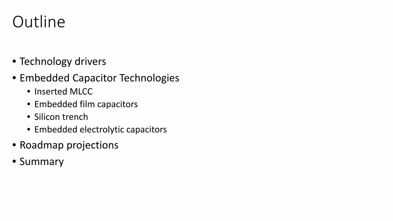
Why capacitor embedding?
System miniaturization
Reduced impedance
Granular power management
Reference: Harvard Univ
Reference: TSMC
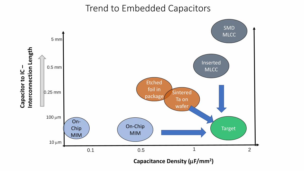
Trend to Embedded Capacitors
Capacitance Density (µF/mm2)
Capa
cito
r to
IC –
Inte
rcon
nect
ion
Leng
th
10 µm
100 µm
0.25 mm
0.5 mm
5 mm
0.1 0.5 2
On-Chip MIM
On-Chip MIM
Inserted MLCC
Etched foil in
package
SMDMLCC
Sintered Ta on wafer
Target
1
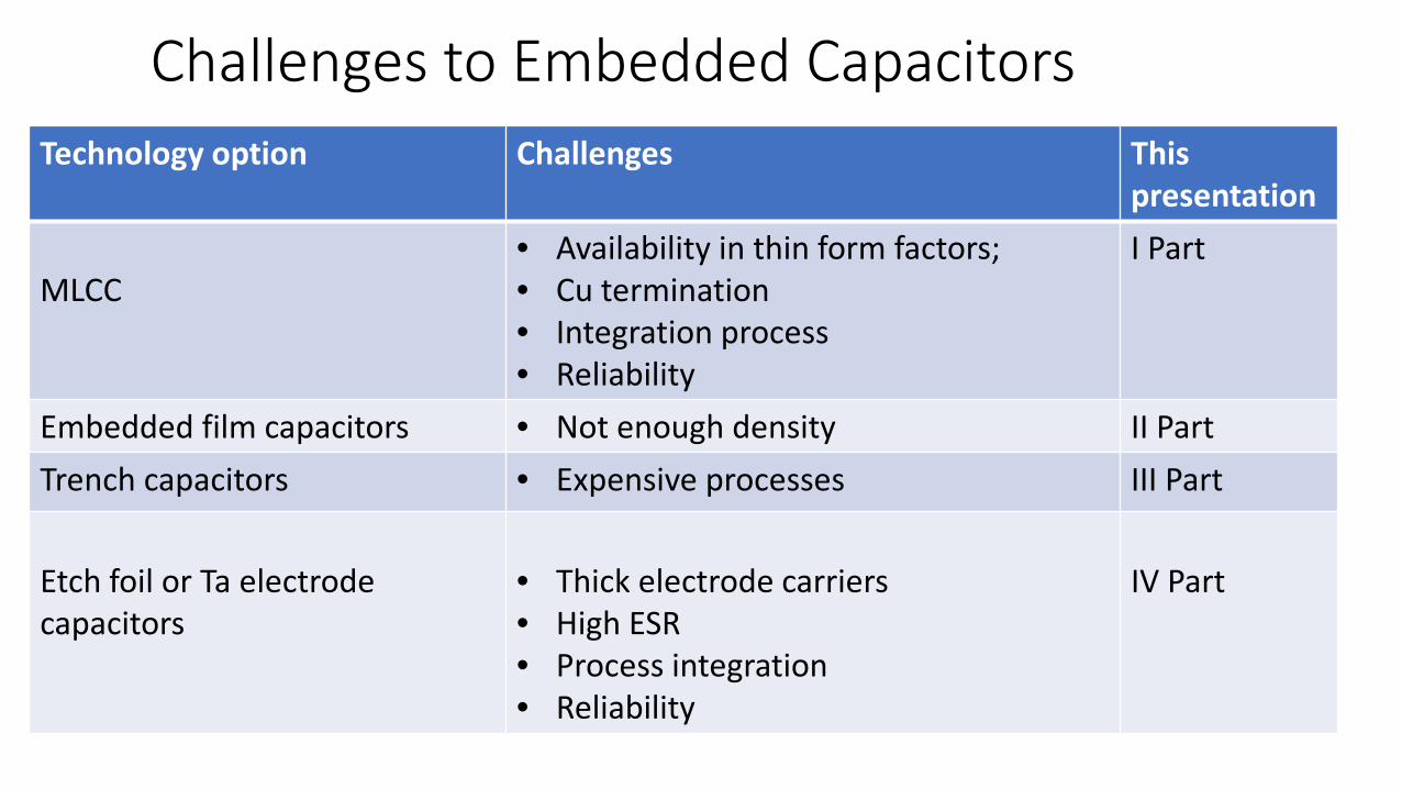
Challenges to Embedded CapacitorsTechnology option Challenges This
presentation
MLCC• Availability in thin form factors; • Cu termination• Integration process• Reliability
I Part
Embedded film capacitors • Not enough density II PartTrench capacitors • Expensive processes III Part
Etch foil or Ta electrode capacitors
• Thick electrode carriers• High ESR• Process integration • Reliability
IV Part
Inserted MLCCs
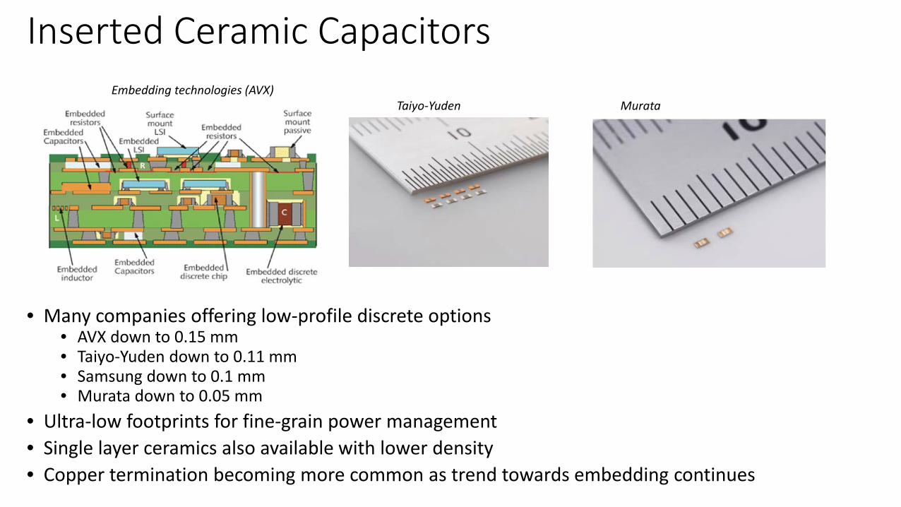
Inserted Ceramic Capacitors
Taiyo-YudenEmbedding technologies (AVX)
• Many companies offering low-profile discrete options• AVX down to 0.15 mm• Taiyo-Yuden down to 0.11 mm• Samsung down to 0.1 mm• Murata down to 0.05 mm
• Ultra-low footprints for fine-grain power management• Single layer ceramics also available with lower density• Copper termination becoming more common as trend towards embedding continues
Murata
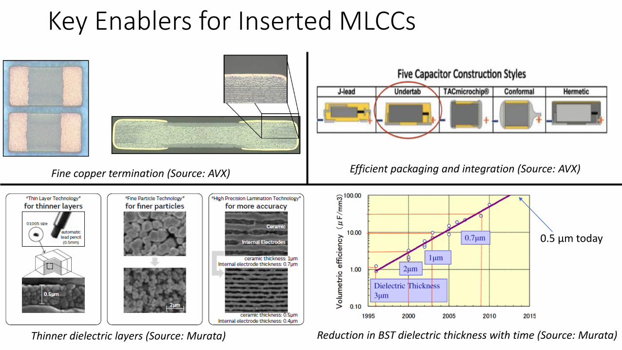
Key Enablers for Inserted MLCCs
Fine copper termination (Source: AVX)
Thinner dielectric layers (Source: Murata) Reduction in BST dielectric thickness with time (Source: Murata)
0.5 µm today
Efficient packaging and integration (Source: AVX)
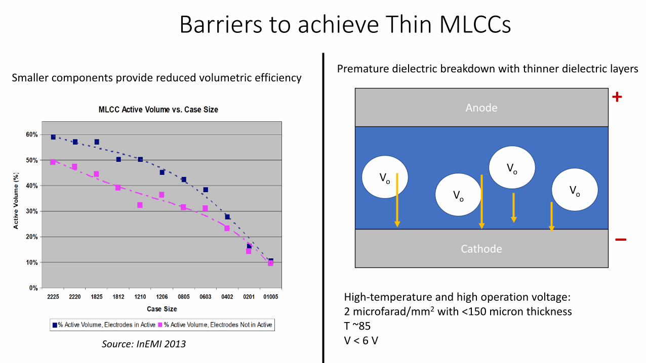
Barriers to achieve Thin MLCCs
Smaller components provide reduced volumetric efficiency
Source: InEMI 2013
Premature dielectric breakdown with thinner dielectric layers
Anode
Cathode
Vo
Vo
Vo
–
+
Vo
High-temperature and high operation voltage:2 microfarad/mm2 with <150 micron thicknessT ~85V < 6 V
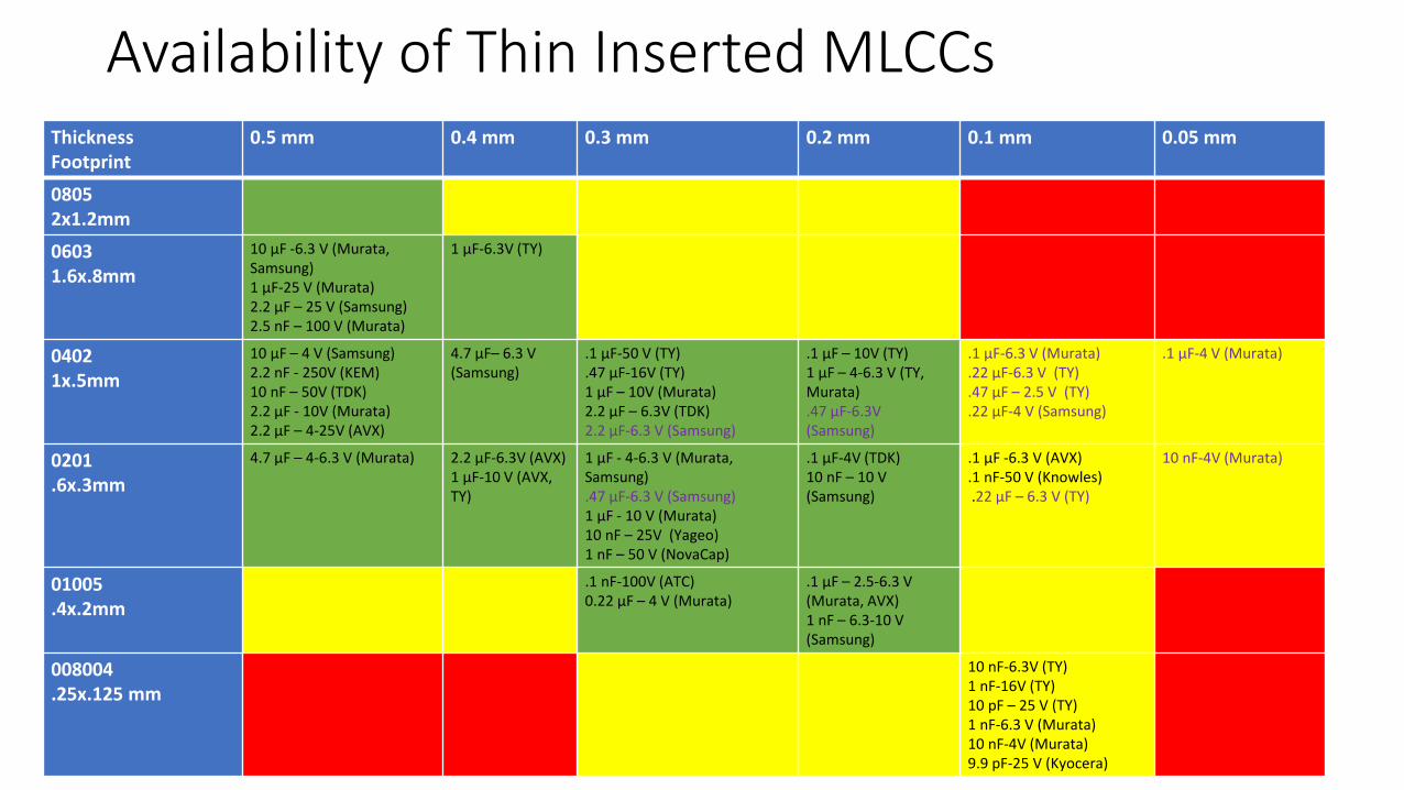
Availability of Thin Inserted MLCCsThicknessFootprint
0.5 mm 0.4 mm 0.3 mm 0.2 mm 0.1 mm 0.05 mm
08052x1.2mm
06031.6x.8mm
10 µF -6.3 V (Murata, Samsung)1 µF-25 V (Murata)2.2 µF – 25 V (Samsung)2.5 nF – 100 V (Murata)
1 µF-6.3V (TY)
04021x.5mm
10 µF – 4 V (Samsung)2.2 nF - 250V (KEM)10 nF – 50V (TDK)2.2 µF - 10V (Murata)2.2 µF – 4-25V (AVX)
4.7 µF– 6.3 V (Samsung)
.1 µF-50 V (TY)
.47 µF-16V (TY)1 µF – 10V (Murata)2.2 µF – 6.3V (TDK)2.2 µF-6.3 V (Samsung)
.1 µF – 10V (TY)1 µF – 4-6.3 V (TY, Murata).47 µF-6.3V (Samsung)
.1 µF-6.3 V (Murata)
.22 µF-6.3 V (TY)
.47 µF – 2.5 V (TY)
.22 µF-4 V (Samsung)
.1 µF-4 V (Murata)
0201.6x.3mm
4.7 µF – 4-6.3 V (Murata) 2.2 µF-6.3V (AVX)1 µF-10 V (AVX, TY)
1 µF - 4-6.3 V (Murata, Samsung).47 µF-6.3 V (Samsung)1 µF - 10 V (Murata)10 nF – 25V (Yageo)1 nF – 50 V (NovaCap)
.1 µF-4V (TDK)10 nF – 10 V (Samsung)
.1 µF -6.3 V (AVX)
.1 nF-50 V (Knowles).22 µF – 6.3 V (TY)
10 nF-4V (Murata)
01005.4x.2mm
.1 nF-100V (ATC)0.22 µF – 4 V (Murata)
.1 µF – 2.5-6.3 V(Murata, AVX)1 nF – 6.3-10 V (Samsung)
008004.25x.125 mm
10 nF-6.3V (TY)1 nF-16V (TY)10 pF – 25 V (TY)1 nF-6.3 V (Murata)10 nF-4V (Murata)9.9 pF-25 V (Kyocera)
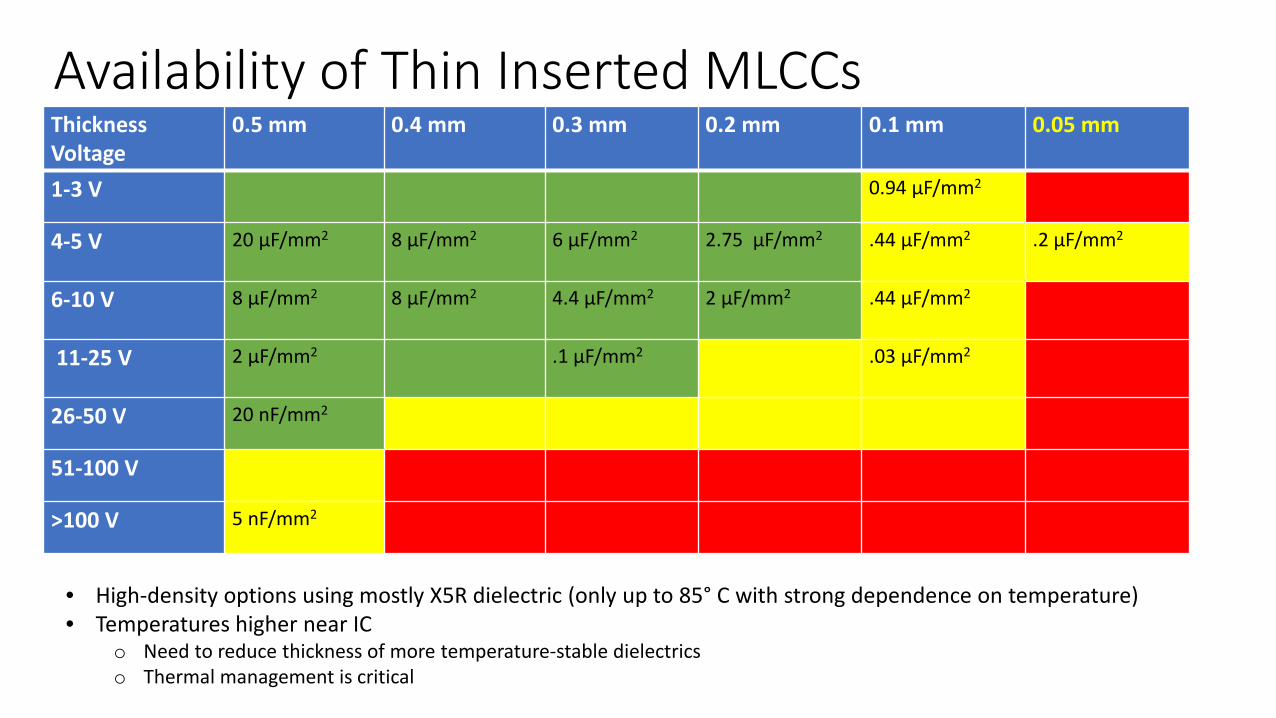
Availability of Thin Inserted MLCCsThicknessVoltage
0.5 mm 0.4 mm 0.3 mm 0.2 mm 0.1 mm 0.05 mm
1-3 V 0.94 µF/mm2
4-5 V 20 µF/mm2 8 µF/mm2 6 µF/mm2 2.75 µF/mm2 .44 µF/mm2 .2 µF/mm2
6-10 V 8 µF/mm2 8 µF/mm2 4.4 µF/mm2 2 µF/mm2 .44 µF/mm2
11-25 V 2 µF/mm2 .1 µF/mm2 .03 µF/mm2
26-50 V 20 nF/mm2
51-100 V
>100 V 5 nF/mm2
• High-density options using mostly X5R dielectric (only up to 85° C with strong dependence on temperature)• Temperatures higher near IC
o Need to reduce thickness of more temperature-stable dielectricso Thermal management is critical
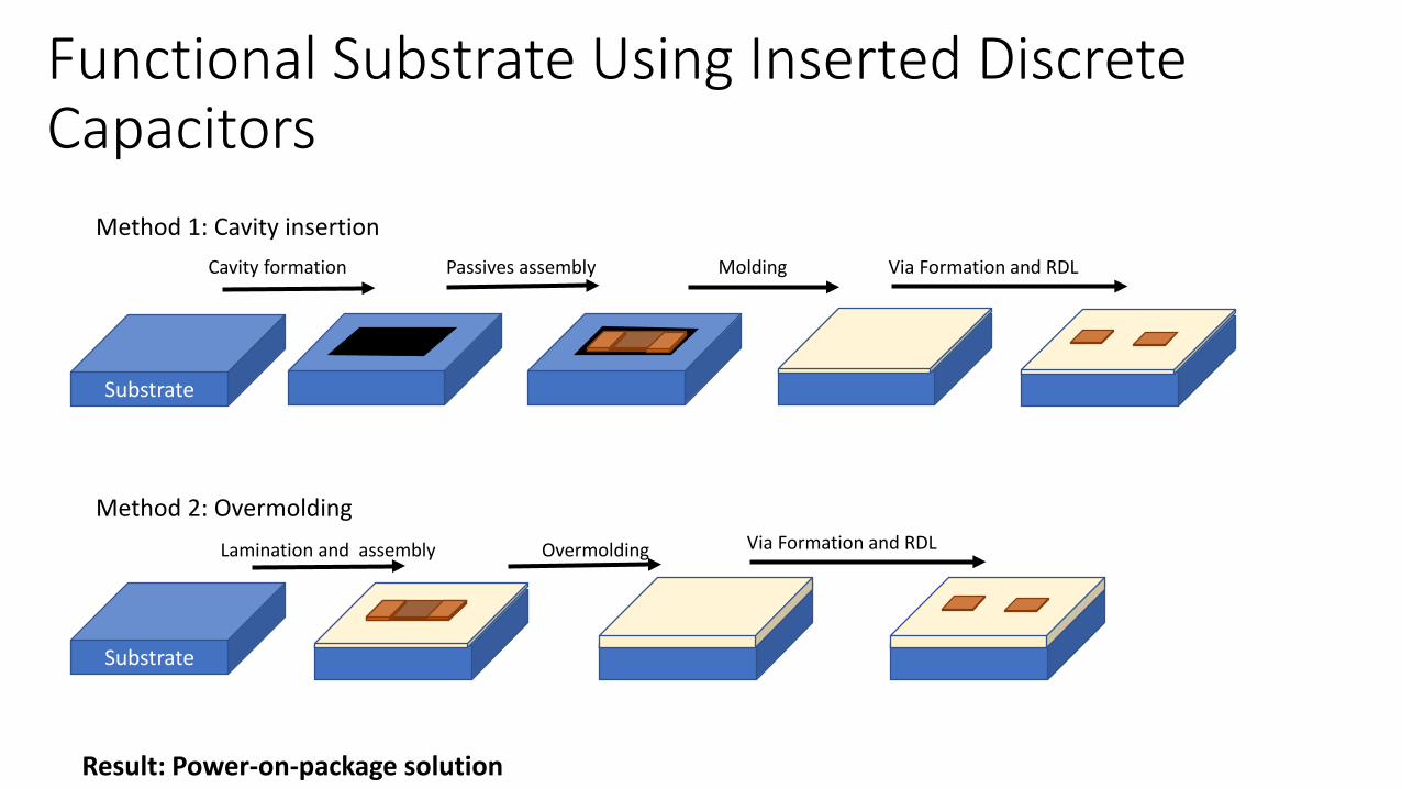
Functional Substrate Using Inserted Discrete Capacitors
Substrate
Cavity formation Passives assembly Molding Via Formation and RDL
Substrate
Lamination and assembly Overmolding Via Formation and RDL
Method 1: Cavity insertion
Method 2: Overmolding
Result: Power-on-package solution
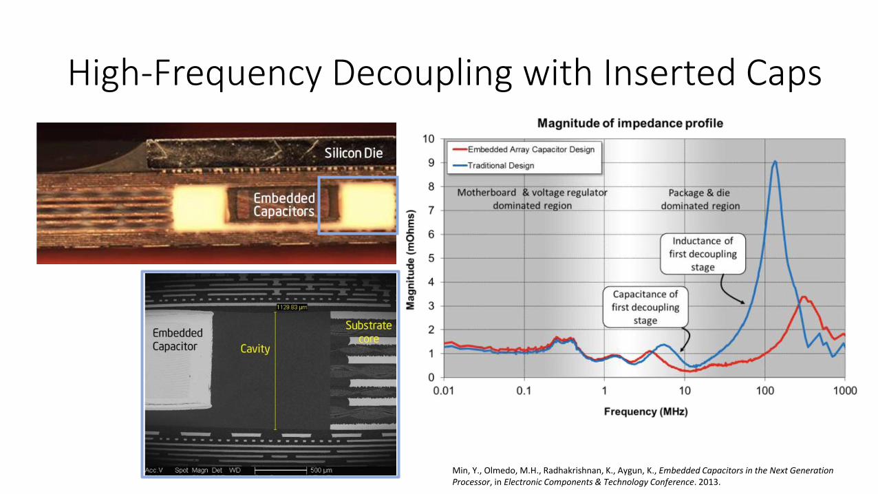
High-Frequency Decoupling with Inserted Caps
Min, Y., Olmedo, M.H., Radhakrishnan, K., Aygun, K., Embedded Capacitors in the Next Generation Processor, in Electronic Components & Technology Conference. 2013.
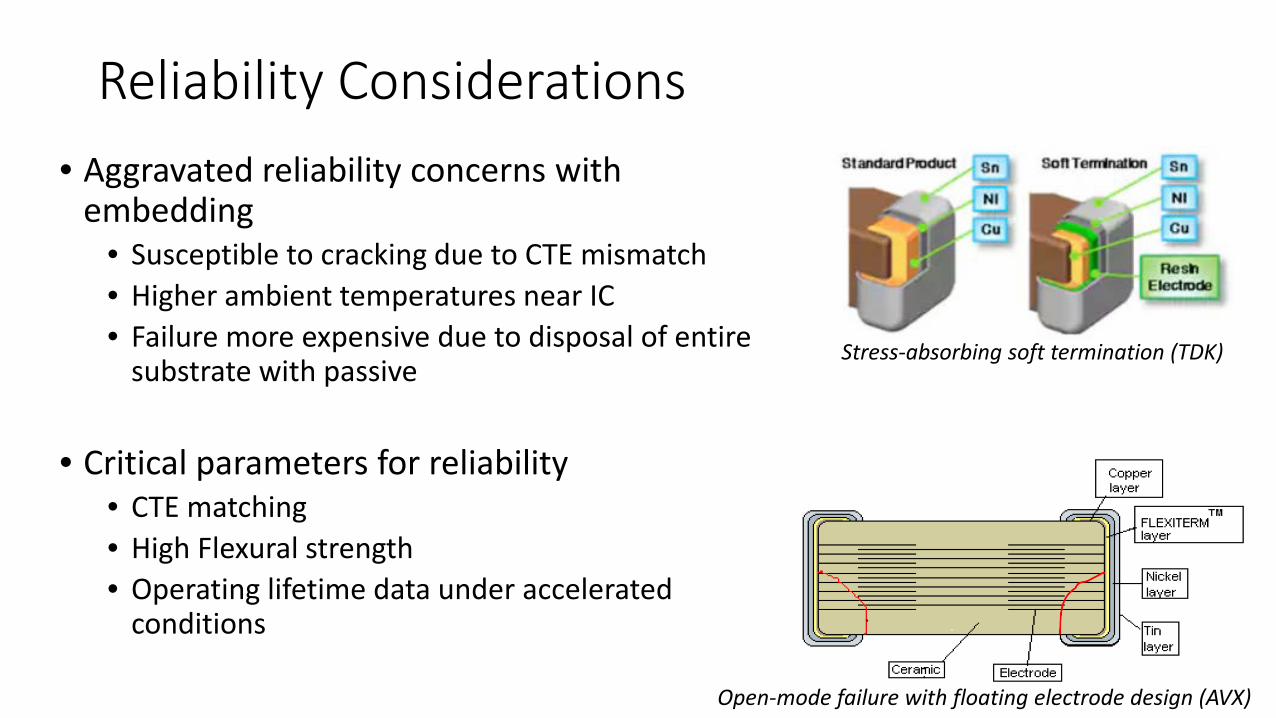
Reliability Considerations• Aggravated reliability concerns with
embedding• Susceptible to cracking due to CTE mismatch• Higher ambient temperatures near IC• Failure more expensive due to disposal of entire
substrate with passive
• Critical parameters for reliability• CTE matching• High Flexural strength• Operating lifetime data under accelerated
conditions
Open-mode failure with floating electrode design (AVX)
Stress-absorbing soft termination (TDK)
Formed Film Capacitors
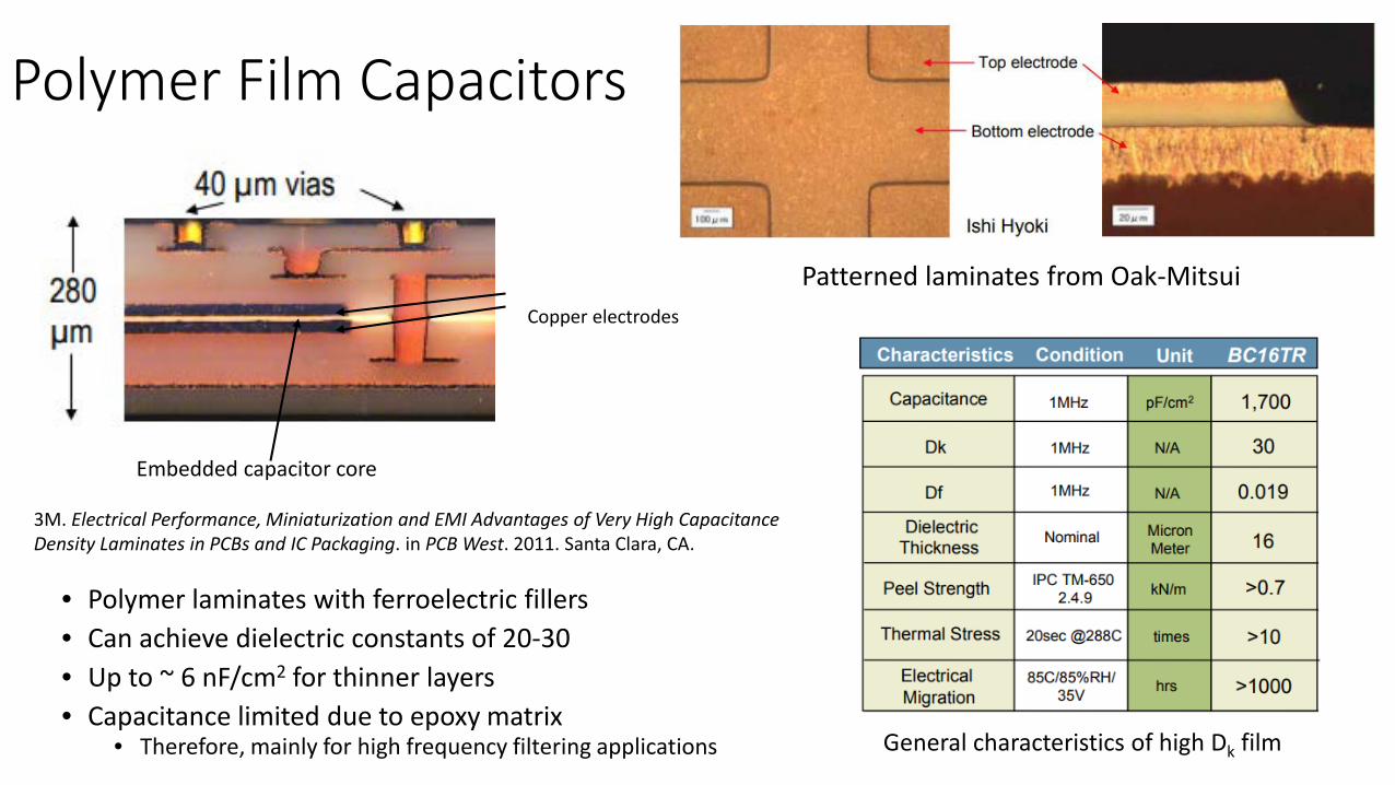
Polymer Film Capacitors
Embedded capacitor core
Copper electrodes
• Polymer laminates with ferroelectric fillers• Can achieve dielectric constants of 20-30• Up to ~ 6 nF/cm2 for thinner layers• Capacitance limited due to epoxy matrix
• Therefore, mainly for high frequency filtering applications
3M. Electrical Performance, Miniaturization and EMI Advantages of Very High Capacitance Density Laminates in PCBs and IC Packaging. in PCB West. 2011. Santa Clara, CA.
Patterned laminates from Oak-Mitsui
General characteristics of high Dk film
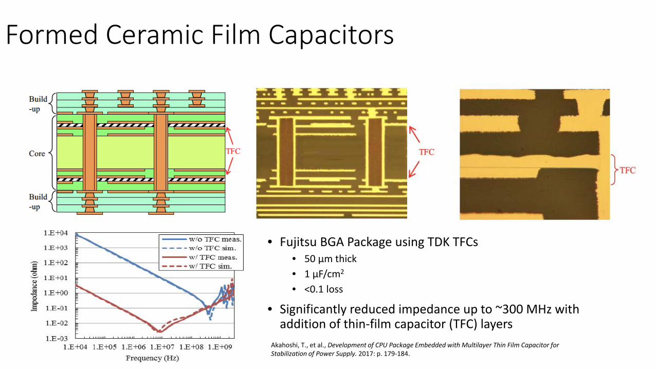
Formed Ceramic Film Capacitors
• Fujitsu BGA Package using TDK TFCs• 50 µm thick• 1 µF/cm2
• <0.1 loss
• Significantly reduced impedance up to ~300 MHz with addition of thin-film capacitor (TFC) layers
Akahoshi, T., et al., Development of CPU Package Embedded with Multilayer Thin Film Capacitor for Stabilization of Power Supply. 2017: p. 179-184.
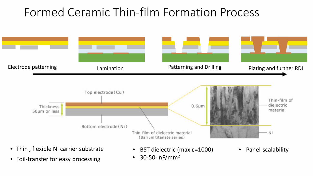
Formed Ceramic Thin-film Formation Process
• Thin , flexible Ni carrier substrate• Foil-transfer for easy processing
• BST dielectric (max ε=1000)• 30-50- nF/mm2
• Panel-scalability
Electrode patterning Lamination Patterning and Drilling Plating and further RDL
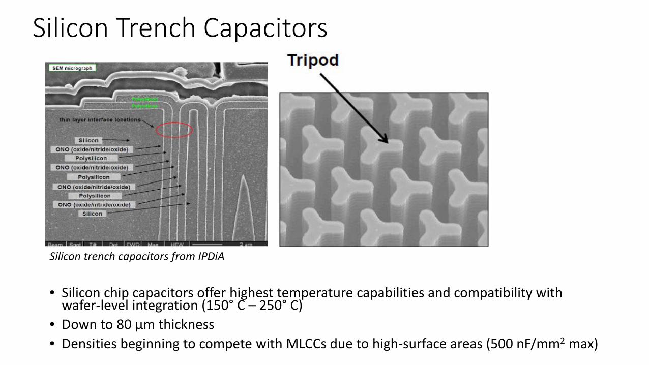
Silicon Trench Capacitors
• Silicon chip capacitors offer highest temperature capabilities and compatibility with wafer-level integration (150° C – 250° C)
• Down to 80 µm thickness• Densities beginning to compete with MLCCs due to high-surface areas (500 nF/mm2 max)
Silicon trench capacitors from IPDiA
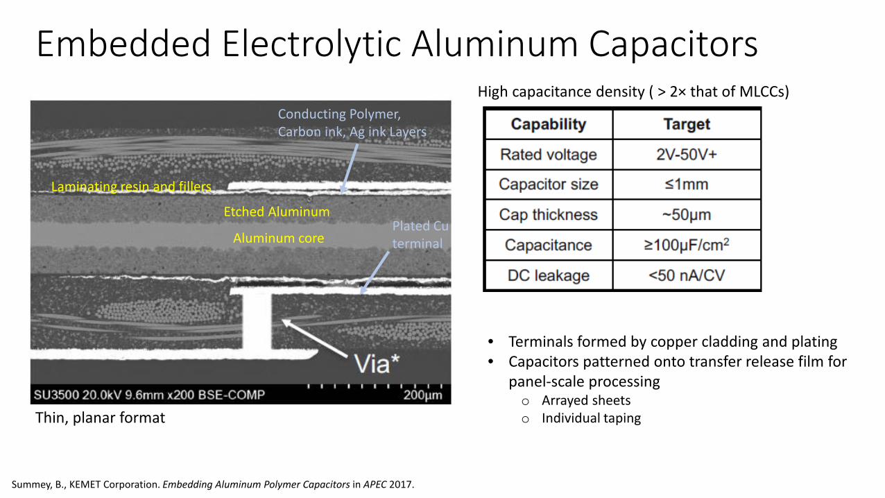
Embedded Electrolytic Aluminum Capacitors
Etched Aluminum
Laminating resin and fillers
Conducting Polymer, Carbon ink, Ag ink Layers
Plated Cu terminalAluminum core
• Terminals formed by copper cladding and plating• Capacitors patterned onto transfer release film for
panel-scale processingo Arrayed sheetso Individual tapingThin, planar format
High capacitance density ( > 2× that of MLCCs)
Summey, B., KEMET Corporation. Embedding Aluminum Polymer Capacitors in APEC 2017.
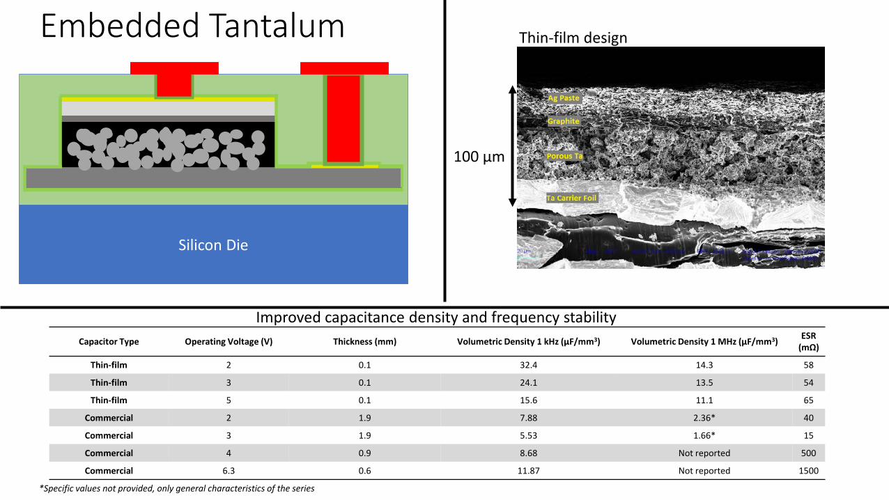
Embedded Tantalum
Capacitor Type Operating Voltage (V) Thickness (mm) Volumetric Density 1 kHz (µF/mm3) Volumetric Density 1 MHz (µF/mm3) ESR (mΩ)
Thin-film 2 0.1 32.4 14.3 58
Thin-film 3 0.1 24.1 13.5 54
Thin-film 5 0.1 15.6 11.1 65
Commercial 2 1.9 7.88 2.36* 40
Commercial 3 1.9 5.53 1.66* 15
Commercial 4 0.9 8.68 Not reported 500
Commercial 6.3 0.6 11.87 Not reported 1500
*Specific values not provided, only general characteristics of the series
100 µm
Thin-film design
Improved capacitance density and frequency stability
Silicon Die
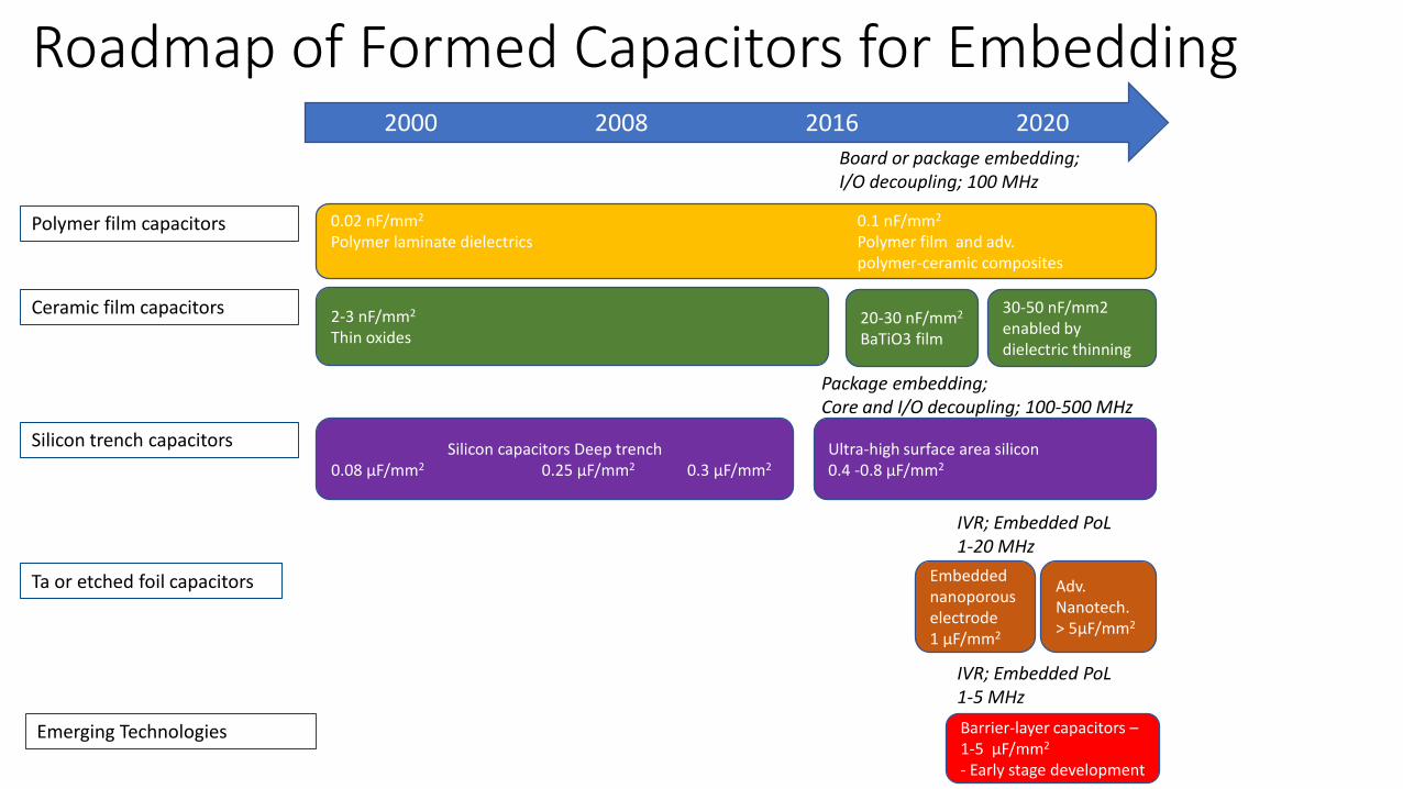
Roadmap of Formed Capacitors for Embedding2000 2008 2016 2020
0.02 nF/mm2 0.1 nF/mm2
Polymer laminate dielectrics Polymer film and adv. polymer-ceramic composites
2-3 nF/mm2
Thin oxides
Embedded nanoporous electrode 1 µF/mm2
Silicon capacitors Deep trench0.08 µF/mm2 0.25 µF/mm2 0.3 µF/mm2
Barrier-layer capacitors –1-5 µF/mm2
- Early stage development
Ceramic film capacitors 30-50 nF/mm2 enabled by dielectric thinning
Polymer film capacitors
Silicon trench capacitors
Ta or etched foil capacitors Adv. Nanotech. > 5µF/mm2
Emerging Technologies
Ultra-high surface area silicon 0.4 -0.8 µF/mm2
20-30 nF/mm2
BaTiO3 film
Board or package embedding;I/O decoupling; 100 MHz
Package embedding;Core and I/O decoupling; 100-500 MHz
IVR; Embedded PoL1-5 MHz
IVR; Embedded PoL1-20 MHz
Summary
• New era of packaging involving embedding of passive components• Reduce system size, lower parasitics, thinner modules• High-frequency noise filtering or decoupling• High-efficiency, fine-grain power management
• Inserted MLCCs becoming more available, enabled by thinner dielectrics and improved process integration
• Silicon trench capacitors for improved thermal and voltage stability, and on-chip integration
• For high-density, embedded electrolytic capacitors in development


![Dimensions: [mm] Recommended Hole Pattern: [mm] Electrical ... · WCAP-FTBE Film Capacitors MPSP075103KA00DCPP45004 ORDER CODE 890493422002CS SIZE REVISION STATUS DATE (YYYY-MM-DD)](https://img.pdfslide.us/doc/110x75/5e20dcef4e03f05b1d7a1268/dimensions-mm-recommended-hole-pattern-mm-electrical-wcap-ftbe-film-capacitors.jpg)