Embed Size (px)
Citation preview
GONG ET AL. VOL. 8 ’ NO. 1 ’ 642–649 ’ 2014
www.acsnano.org
642
November 21, 2013
C 2013 American Chemical Society
Realistic Metal�Graphene ContactStructuresChengGong, StephenMcDonnell, XiaoyeQin, AngelicaAzcatl, HongDong, Yves J. Chabal, Kyeongjae Cho,*
and Robert M. Wallace*
Department of Materials Science and Engineering, The University of Texas at Dallas, Richardson, Texas 75080, United States
The contact resistance for metals tographene continues to be a key lim-itation in device applications. The
low-field electrical transport behavior ofgraphene, characterized by the conductiv-ity (σ) as a function of gate voltage (Vg),shows a characteristic “V shape” with theconductivity minimum indicating the posi-tion of the Dirac point of the graphenechannel.1 Metal electrodes (e.g., Pt or Au)that weakly interact with graphene, withoutchemical bond formation or substantialinterface hybridization, preserve the gra-phene linear π-band dispersion2�5 anddope graphene in the contact regions, lead-ing to n-i-n or p-i-p junction formationthroughout the device.6,7 The conductivitiesof such junctions are expected to have“W shape” with two minima as a functionofVg at theDiracpointsof thedopedand intrin-sic graphene.6,7 This type of contact geo-metry is termed “side-contact”,8�10 oftenassumed to be metal slabs on the pristinegraphene. The junction model, albeit suc-cessful for understanding the electronictransport through the graphene side-contacted by weakly interacting metals,fails to interpret more realistic interfaceswith widely used “wetting” electrodes (viz.,Pd,11,12 Ti,13,14 Cr,15 Ni,16 and Co15). In fact,the weakly interacting metal�graphene in-terfaces pose a practical adhesion problem
causing electronic devices to fail throughdelamination. This is a primary reason thatwetting metals with strong interfacialinteraction are favored in graphene nano-electronics.Nearly all the analysis of the electrical
data from the wetting metal�graphenecontact has been performed based on theside-contact model,12,17,18 which deservescareful scrutiny. Essentially, the wettingelectrodes may affect not only the elec-tronic (i.e., disturbing the π-electron lineardispersion by metal d- and carbon π-orbitalhybridization) but also the structural prop-erties of graphene (e.g., forming a carbide,19
probably initiated by transition metal ada-toms reacting with defect regions20). With-out careful structural characterization, it istherefore risky to assume that grapheneremains intact while in contact with suchreactivemetals. For example, early in carbonnanotube (CNT) research, the Ti-CNT end-contact geometry was proven to be prefer-able at T> 800 �Cby Zhang et al.21 as a resultof the formation of a carbide layer at thecontact, followed by the theoretical investi-gationby Léonard andTersoff.22 Particularly, itis important to note that the electron-beamdeposition process, under carefully controlledambient conditions, contains a number ofreactive metal atoms and nanoclusters thatreadily disrupt the planar sp2-bonded network
* Address correspondence [email protected],[email protected].
Received for review October 8, 2013and accepted November 21, 2013.
Published online10.1021/nn405249n
ABSTRACT The contact resistance of metal�graphene junctions has been actively explored
and exhibited inconsistencies in reported values. The interpretation of these electrical data has
been based exclusively on a side-contact model, that is, metal slabs sitting on a pristine graphene
sheet. Using in situ X-ray photoelectron spectroscopy to study the wetting of metals on as-
synthesized graphene on copper foil, we show that side-contact is sometimes a misleading
picture. For instance, metals like Pd and Ti readily react with graphitic carbons, resulting in
Pd- and Ti-carbides. Carbide formation is associated with C�C bond breaking in graphene, leading
to an end-contact geometry between the metals and the periphery of the remaining graphene patches. This work validates the spontaneous formation of the
metal�graphene end-contact during the metal deposition process as a result of the metal�graphene reaction instead of a simple carbon diffusion process.
KEYWORDS: graphene . metal . interface reaction . carbide . end-contact . X-ray photoelectron spectroscopy
ARTIC
LE
GONG ET AL. VOL. 8 ’ NO. 1 ’ 642–649 ’ 2014
www.acsnano.org
643
of graphene.23 Lahiri et al. experimentally demon-strated the easy formation of nickel carbide at 100 �Cwhen Ni is deposited on the as-synthesized graphene,in sharp contrast to graphene on Ni substrate that canbe stable up to 650 �C.19 Lahiri et al.'s work highlightedthe notable difference between graphene interfacingwith metal substrate and with deposited metals. How-ever, intensive efforts have been mostly focused oncharacterizing the epitaxial graphene on metal tem-plates rather than the graphene covered by depositedmetal layers, even though they can formquite differentinterface structures. At the former interface, grapheneis formed on ametal surface with more commensuratemorphology, but the latter interface formation processismore reactive due to the chemically aggressivemetalatoms and clusters deposited on graphene. Electricalcharacterization, although being widely performed innumerous devices,11�18,24 cannot provide interfacialchemical bonding information. Therefore, it is impor-tant to determine the interfacial chemistry betweengraphene and deposited wetting metals in order toelucidate contact issues.Titanium and palladium are the two representative
wetting metals studied in this work. First, Pd differsfrom other more reactive metals (i.e., Ti, Ni, Cr, and Co)which favor oxidization or carbidization.25,26 Remark-ably, experimental observations reveal that Pd electro-des have a lower contact resistance than Ti electrodeswhen contacting graphene.27 In contrast, most trans-port simulations conclude that Ti is a superior contactover Pd.28�30 Palladium in contact with metallic CNTs(m-CNTs) was claimed to achieve more reliable perfor-mance (i.e., reproducibility) than Ti, which was ascribedto the possible oxidation of Ti in the vacuum environ-ment employed.31 Second, although Pd has a similarelectronic configuration to Pt, these metals behavedifferently in both graphene and CNT electronics.32
Palladium, with a lower work function, was shown toform a p-type Ohmic contact where Pt, with a higherwork function, otherwise formed a non-Ohmic contactwith m-CNTs.31,33 Javey et al. attributed this unexpectedresult to the more favorable interaction between Pd(than Pt) and the CNT sidewall.33 The mechanism of howthe favorable metal interaction promotes the electricalperformance of graphene electronics remains elusive. Xiaet al.'s work12 highlighted the important contribution ofthe charge transport through the graphene underneathPd contact, whereas Mann et al.31 emphasized that thecharge injectionmainly occurs at theedgeofPdcontact tothe CNT. To provide insights for a better understanding ofthese issues, we chose Pd and Ti for this study.
RESULTS AND DISCUSSION
We deposited Pd and Ti separately on as-growngraphene on copper foil at room temperature underultrahigh vacuum (UHV) conditions, followed by anin situ X-ray photoelectron spectroscopy (XPS) study of
the interfacial bonding chemistry. In order to probe thereal interaction between deposited metals and gra-phene, three precautionswere taken. (i) The depositionchamber ambient condition must be under very lowpressures (∼10�9mbar) to avoid spurious oxidation and/or catalyzed carbidization with residual water typicallypresent in elastomer-sealed evaporators, particularly forTi deposition;34,35 (ii) the graphene samples must beclean, free of carbon or oxygen contamination;36,37 (iii)the metal deposition and XPS characterization processesmust be done without vacuum interruption to avoid orminimize spurious oxidation/contamination. The concur-rent fulfillment of all three precautions rules out theimpact of oxygen- and carbon-bearing contaminants,from either the deposition chamber26 or the graphenesurface.38 Therefore, in the series of experiments reportedhere, a clustered UHV system39 is utilized to providethe following conditions: (i) e10�9 mbar is maintainedin the UHV cluster, including the deposition chamber(∼1� 10�9mbar), XPS chamber (∼3� 10�10mbar), andthe transfer tube (∼2� 10�11 mbar) connecting the twochambers; and (ii) as-grown graphene on a copper foil27
is used instead of the polymer-aided transferred gra-phene on SiO2 where residues are evident.36,40 Onlythrough the careful control of these conditions can XPSdata be reliably translated into an understanding of themetal�graphene interaction.
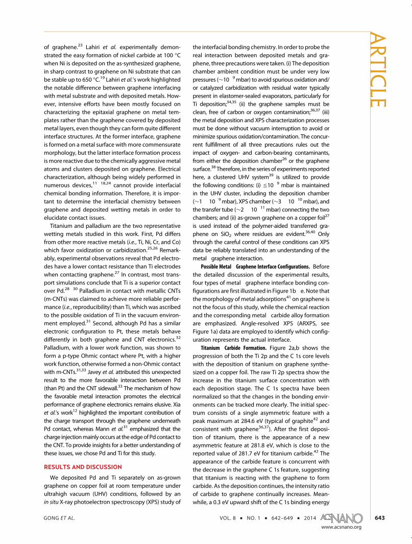
Possible Metal�Graphene Interface Configurations. Beforethe detailed discussion of the experimental results,four types of metal�graphene interface bonding con-figurations are first illustrated in Figure 1b�e. Note thatthemorphology of metal adsorptions41 on graphene isnot the focus of this study, while the chemical reactionand the corresponding metal�carbide alloy formationare emphasized. Angle-resolved XPS (ARXPS, seeFigure 1a) data are employed to identify which config-uration represents the actual interface.
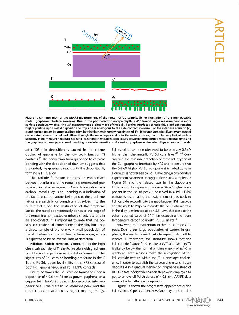
Titanium�Carbide Formation. Figure 2a,b shows theprogression of both the Ti 2p and the C 1s core levelswith the deposition of titanium on graphene synthe-sized on a copper foil. The raw Ti 2p spectra show theincrease in the titanium surface concentration witheach deposition stage. The C 1s spectra have beennormalized so that the changes in the bonding envir-onments can be tracked more clearly. The initial spec-trum consists of a single asymmetric feature with apeak maximum at 284.6 eV (typical of graphite42 andconsistent with graphene36,37). After the first deposi-tion of titanium, there is the appearance of a newasymmetric feature at 281.8 eV, which is close to thereported value of 281.7 eV for titanium carbide.42 Theappearance of the carbide feature is concurrent withthe decrease in the graphene C 1s feature, suggestingthat titanium is reacting with the graphene to formcarbide. As the deposition continues, the intensity ratioof carbide to graphene continually increases. Mean-while, a 0.3 eV upward shift of the C 1s binding energy
ARTIC
LE
GONG ET AL. VOL. 8 ’ NO. 1 ’ 642–649 ’ 2014
www.acsnano.org
644
after 105 min deposition is caused by the n-typedoping of graphene by the low work function Ticontacts.24 The conversion from graphene to carbidicbonding with the deposition of titanium suggests thatthe underlying graphene reacts with the deposited Ti,forming a Ti�C alloy.
This carbide formation indicates an end-contactbetween titanium and the remaining nonreacted gra-phene (illustrated in Figure 2f). Carbide formation, as acarbon�metal alloy, is an unambiguous indication ofthe fact that carbon atoms belonging to the graphenelattice are partially or completely dissolved into thebulk metal. Upon the destruction of the graphenelattice, the metal spontaneously bonds to the edge ofthe remaining nonreacted graphene sheet, resulting inan end-contact. It is important to note that the ob-served carbide peak corresponds to the alloy but is nota direct sample of the relatively small population ofmetal�carbon bonding at the graphene edges, whichis expected to be below the limit of detection.
Palladium�Carbide Formation. Compared to the highchemical reactivity of Ti, the Pd reaction with grapheneis subtle and requires more careful examination. Thesignatures of Pd�carbide bonding are found in the C1s and Pd 3d5/2 core level shifts in the XPS spectra ofboth Pd�graphene/Cu and Pd�HOPG contacts.
Figure 2c shows the Pd�carbide formation upon adeposition of ∼0.6 nm Pd on as-grown graphene on acopper foil. The Pd 3d peak is deconvoluted into twopeaks: one is the metallic Pd reference peak, and theother is located at a 0.6 eV higher binding energy.
Pd�carbide has been observed to be typically 0.6 eVhigher than the metallic Pd 3d core level.43�45 Con-sidering the minimal detection of remnant oxygen atthe Cu�graphene interface by XPS and to ensure thatthe 0.6 eV higher Pd 3d component (shaded zone inFigure 2c) is not causedbyPd�Obonding, a comparativeexperiment is doneon anoxygen-freeHOPG sample (seeFigure S1 and the related text in the SupportingInformation). In Figure 2c, the same 0.6 eV higher com-ponent in the Pd 3d peak is observed in a Pd�HOPGcontact, substantiating the assignment of this peak toPd�carbide. According to the ratio between Pd�carbideand themetallic Pd peak intensity, the Pd�C atomic ratioin the alloy is estimated to be∼5.5:1, which is close to theother reported value of 6:1,43 far exceeding the roomtemperature carbon solubility (<0.1%) in Pd.46
Now we turn our attention to the Pd�carbide C 1speak. Due to the large population of carbon in gra-phene, the newly formed carbide signal is difficult toresolve. Furthermore, the literature shows that thePd�carbide feature for C 1s (284.3 eV47 and 284.1 eV48)is slightly below the normal binding energy of sp2-C ingraphene. Both reasons make the recognition of thePd�carbide feature within the C 1s envelope challen-ging. In order to establish the carbide chemical shift, wedeposit Pd in a gradual manner on graphene instead ofHOPG: a total of eight deposition stepswere employed toget to an overall Pd thickness of ∼2.5 nm. ARXPS datawere collected after each deposition.
Figure 3a shows the progressive appearance of thePd�carbide C peak at 284.0 eV. One may question the
Figure 1. (a) Illustration of the ARXPS measurement of the metal�Gr/Cu sample. (b�e) Illustration of the four possiblemetal�graphene interface scenarios. Due to the photoelectron escape depth, a 45� takeoff angle measurement is moresurface sensitive, whereas the 75� measurement probes more of the bulk. For the interface scenario (b), graphene remainshighly pristine upon metal deposition on top and is analogous to the side-contact scenario. For the interface scenario (c),graphenemaintains its structural integrity, but the flatness is somewhat distorted. For interface scenario (d), a tiny amount ofcarbon atoms are extracted and diffuse through the metal layers and onto the metal surfaces, due to the very limited carbonsolubility in themetal. For interface scenario (e), strong chemical reaction occurs between the depositedmetal and graphene, andthe graphene is thereby consumed, resulting in carbide formation and a metal�graphene end-contact. Figures are not to scale.
ARTIC
LE
GONG ET AL. VOL. 8 ’ NO. 1 ’ 642–649 ’ 2014
www.acsnano.org
645
assignment of the 284.0 and 335.7 eV peaks to be the Cpeak and Pd peak in Pd�carbide; that is, can thegraphene film covered by palladium without Pd�Calloy formation (as represented by Figure 1b,c) lead tothe detected peaks? In other words, is it possible toobserve a chemical shift 0.6 eV higher for the Pd peakand a 0.6 eV lower C peak by simply stacking Pd on thegraphene sheet without any chemical reaction? Weattribute these two peaks to the Pd�C alloy (i.e.,Pd�carbide). Angle-resolvedXPSprovides the convincing
evidence that (i) the detected C peak is not from theinterface but from the surface, and (ii) the detected Pdpeak is not from the interfacebut fromauniformalloy alsoon the surface. For convenience, the peak correspondingto the carbon in graphene at∼284.6 eV is labeled “C�C”';the peak corresponding to the carbon in the Pd�carbideat∼284.0 eV is labeled “C�Pd”; thepeakcorresponding tothe Pd in the Pd�carbide at∼335.7 eV is labeled “Pd�C”,and the peak corresponding to the metallic Pd referenceat 335.1 eV is labeled “Pd�Pd”. Themetallic Pd reference is
Figure 2. (a) Ti 2p and (b) C 1s XPS spectra for the 30min (∼0.6 nm), 60min (∼1.5 nm), and 105min (∼3.0 nm) deposition of Tion as-grownGr/Cu. (c) Pd 3d5/2 XPS spectra for the Pddepositiononas-grownGr/Cu (∼0.6 nmPd) andHOPG (∼0.8 nmPd) and(d) C 1s XPS spectra for∼0.1 and∼0.4 nmPd deposition on as-grownGr/Cu. The schematic illustration ofmetal�graphene (e)side-contact and (f) end-contact structures. The white dots in (f) represent the carbon atoms in the metal�carbide alloy.
ARTIC
LE
GONG ET AL. VOL. 8 ’ NO. 1 ’ 642–649 ’ 2014
www.acsnano.org
646
obtained by depositing a suitable thickness (tens ofnanometers) of Pd on a pure Cu surface.
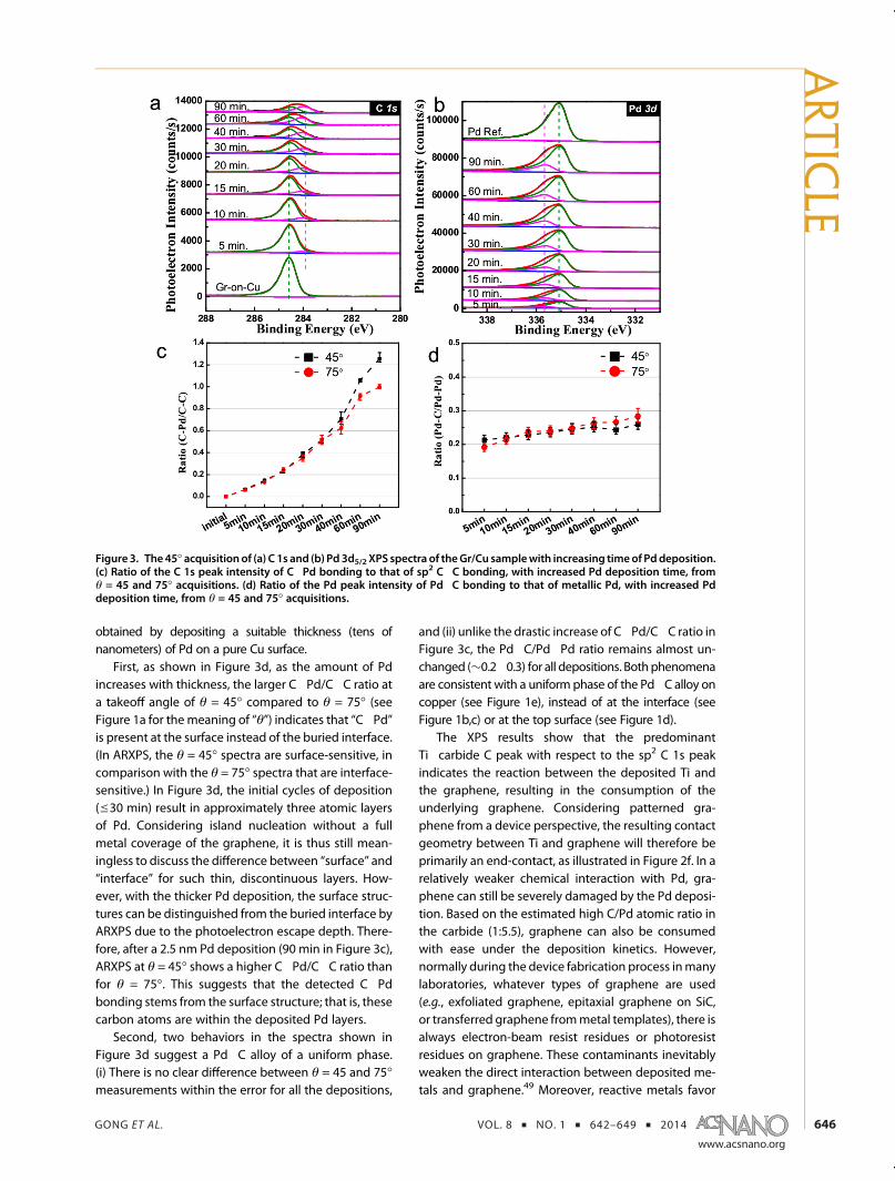
First, as shown in Figure 3d, as the amount of Pdincreases with thickness, the larger C�Pd/C�C ratio ata takeoff angle of θ = 45� compared to θ = 75� (seeFigure 1a for themeaning of “θ”) indicates that “C�Pd”is present at the surface instead of the buried interface.(In ARXPS, the θ = 45� spectra are surface-sensitive, incomparison with the θ = 75� spectra that are interface-sensitive.) In Figure 3d, the initial cycles of deposition(e30 min) result in approximately three atomic layersof Pd. Considering island nucleation without a fullmetal coverage of the graphene, it is thus still mean-ingless to discuss the difference between “surface” and“interface” for such thin, discontinuous layers. How-ever, with the thicker Pd deposition, the surface struc-tures can be distinguished from the buried interface byARXPS due to the photoelectron escape depth. There-fore, after a 2.5 nm Pd deposition (90 min in Figure 3c),ARXPS at θ = 45� shows a higher C�Pd/C�C ratio thanfor θ = 75�. This suggests that the detected C�Pdbonding stems from the surface structure; that is, thesecarbon atoms are within the deposited Pd layers.
Second, two behaviors in the spectra shown inFigure 3d suggest a Pd�C alloy of a uniform phase.(i) There is no clear difference between θ = 45 and 75�measurements within the error for all the depositions,
and (ii) unlike the drastic increase of C�Pd/C�C ratio inFigure 3c, the Pd�C/Pd�Pd ratio remains almost un-changed (∼0.2�0.3) for all depositions. Bothphenomenaare consistent with a uniform phase of the Pd�C alloy oncopper (see Figure 1e), instead of at the interface (seeFigure 1b,c) or at the top surface (see Figure 1d).
The XPS results show that the predominantTi�carbide C peak with respect to the sp2 C 1s peakindicates the reaction between the deposited Ti andthe graphene, resulting in the consumption of theunderlying graphene. Considering patterned gra-phene from a device perspective, the resulting contactgeometry between Ti and graphene will therefore beprimarily an end-contact, as illustrated in Figure 2f. In arelatively weaker chemical interaction with Pd, gra-phene can still be severely damaged by the Pd deposi-tion. Based on the estimated high C/Pd atomic ratio inthe carbide (1:5.5), graphene can also be consumedwith ease under the deposition kinetics. However,normally during the device fabrication process inmanylaboratories, whatever types of graphene are used(e.g., exfoliated graphene, epitaxial graphene on SiC,or transferred graphene frommetal templates), there isalways electron-beam resist residues or photoresistresidues on graphene. These contaminants inevitablyweaken the direct interaction between deposited me-tals and graphene.49 Moreover, reactive metals favor
Figure 3. The 45� acquisitionof (a) C 1s and (b) Pd 3d5/2 XPS spectra of theGr/Cu samplewith increasing timeof Pddeposition.(c) Ratio of the C 1s peak intensity of C�Pd bonding to that of sp2 C�C bonding, with increased Pd deposition time, fromθ = 45 and 75� acquisitions. (d) Ratio of the Pd peak intensity of Pd�C bonding to that of metallic Pd, with increased Pddeposition time, from θ = 45 and 75� acquisitions.
ARTIC
LE
GONG ET AL. VOL. 8 ’ NO. 1 ’ 642–649 ’ 2014
www.acsnano.org
647
oxidization and carbidization in non-UHV depositionconditions.34,35 Therefore, the metal�graphene con-tact in many as-prepared devices may be a compli-cated combination of both end-contact and side-contact interactions. One may expect a varying per-centage of end-contact configuration from device todevice, depending on themetals (e.g., purity, reactivity,etc.), the deposition conditions (e.g., vacuum levels,deposition temperatures, etc.), the sample qualities(e.g., graphene cleanness), and the post-annealing.
Palladium�Graphene Reaction. The formation of Pd�carbide originates from a strong interface chemicalreaction, instead of a simple process of carbon diffu-sion into metals, considering that the room tempera-ture carbon solubility in Pd is even lower than 0.1%.46
The chemical interaction between hydrocarbons andPd surfaces has been reported with the formation ofsurface Pd�carbide.44,45 The other evidence in supportof the reaction mechanism rather than the diffusionmechanism is the observation that the ratio of Pd�carbide XPS signal to the metallic Pd XPS signal isincreased by depositing Pd on a defective graphene. Itis known that the reactivity of graphene is effectivelyenhanced by making it defective. Through predeposi-tion helium ion bombardment on a separate sample,we show that there is an increased carbon concentra-tion in the resulting Pd�carbide.
An ion gun (model FIG-SCE 5 kV Physical Electronics,Inc.) was used to perform sputtering using helium as thesource. The sputtering lasted for 2 min at a beam voltageof 1 kV, with a spot size of 4 � 4 mm. The X-ray photo-electron spectrometer and the ion gun are located in thesame chamber. XPS was taken before and after Hesputtering in the same region. After Pd was depositedon the sample in the metal deposition chamber andtransferred to the XPS analysis chamber, the position
was monitored and precisely controlled so that XPS wastaken in the same sputtered spot.
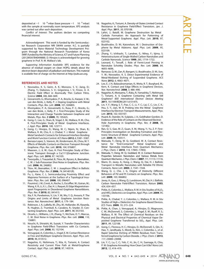
After He ion sputtering the as-synthesized CVDgraphene on copper foil,∼0.9 nm thick Pd was depos-ited. In this UHV environment, a number of defects inthe graphene sheet are produced after He ion sputter-ing, promoting the reactivity of graphene. Therefore, insitu Pd deposition on the sputtered graphene sheetinvolves a stronger chemical reaction between Pd andgraphene. The XPS data in Figure 4 show an increasedPd�C/Pd�Pd ratio (∼1.5), compared with the Pddeposition on as-synthesized graphene (∼0.25, asshown in Figure 2c and 3b,d). This result is strongevidence that the Pd�graphene chemical reaction isdependent on the reactivity of the graphene.
CONCLUSION
In summary, in situ XPS characterization of electron-beam-deposited Pd and Ti on as-synthesized grapheneon copper in a UHV environment provides unambiguousevidence that the sp2-bonded planar structure of gra-phene is disrupted by the wetting metal�graphenechemical interaction. The end-contact configuration isformed between metals and the nonreacted graphene.To generalize the impact of this work, we suspect that thebroadly adopted metal�graphene side-contact modelconveys physically misleading information. When wettingmetals such as Pd and Ti are intended to be deposited ongraphene, two likely results would be gained. The firstpossible outcome is the strong chemical interaction andthe resulting metal�carbide; that is, graphene is con-sumed. The second possible outcome is the oxidizationandcarbidizationof thedepositedmetal by theoxygen-orcarbon-bearing contaminants in the chamber or on thegraphene, resulting inmetal�oxide� ormetal�carbide�graphene contact. Basically, the pure wetting metal�gra-phene interface in side-contact geometry is not expectedto occur as a result of the reactive metal depositionprocess. Efforts on the fabrication of metal�grapheneend-contact29,50 have been devotedwith reduced contactresistances demonstrated.13,51 Recently, a study ofmetal�graphene end-contact has been reported.52 In contrast tothese reports, this work provides experimental validationof the spontaneous formation of end-contacts whenwetting metals are deposited on clean graphene filmsunder well-controlled vacuum conditions.
EXPERIMENTAL METHODOLOGIES
Graphene Synthesis, Metal Deposition, and XPS Characterization. TheCVD graphene samples employed in this work were grown on25 μm thick Cu foils (Alfa Aesar, 99.8% purity) in a halogen lamp-based quartz tube furnace at a growth temperature of 1035 �Cwith 5 sccm of H2 and 7 sccm of CH4 flowing during growthwith a total pressure of 400 Torr.36,53 Graphene grown by thismethod has a grain size of 10�20 μm as determined byscanning electron microscope imaging. The samples were then
loaded into the cluster XPS analysis chamber, where analysiswas carried out using a monochromatic Al KR X-ray source.39
An analyzer acceptance angle of 8�, a takeoff angle of 45�(by default) or 75� (angle between the detector and the samplesurface in ARXPS study), and pass energy of 15 eV wereemployed in this study. Pd and Ti were deposited on the as-synthesized graphene with an electron-beam evaporationsource in a UHV chamber connected to the analysis chamberand were outgassed for 2 h prior to deposition to avoid anymetal oxide remnants at the surface. The metal Pd and Ti were
Figure 4. XPS spectrum of Pd 3d5/2 core level shift after∼0.9 nm Pd deposition on He-sputtered (reactive) CVDgraphene.
ARTIC
LE
GONG ET AL. VOL. 8 ’ NO. 1 ’ 642–649 ’ 2014
www.acsnano.org
648
deposited at ∼1 � 10�8 mbar (base pressure ∼1 � 10�9 mbar)with the sample at nominally room temperature. XPS analysiswas carried out after each deposition.
Conflict of Interest: The authors declare no competingfinancial interest.
Acknowledgment. This work is funded by the Semiconduc-tor Research Corporation NRI SWAN center. K.C. is partiallysupported by Nano 3Material Technology Development Pro-gram through the National Research Foundation of Korea(NRF) fundedby theMinistry of Science, ICT and Future Planning(2012M3A7B4049888). D. Hinojos is acknowledged for growinggraphene in Prof. R. M. Wallace's lab.
Supporting Information Available: XPS evidence for theabsence of residual oxygen on clean HOPG; details about theelectron-beamdeposition of palladium and titanium. Thismaterialis available free of charge via the Internet at http://pubs.acs.org.
REFERENCES AND NOTES1. Novoselov, K. S.; Geim, A. K.; Morozov, S. V.; Jiang, D.;
Zhang, Y.; Dubonos, S. V.; Grigorieva, I. V.; Firsov, A. A.Electric Field Effect in Atomically Thin Carbon Films.Science 2004, 306, 666–669.
2. Giovannetti, G.; Khomyakov, P. A.; Brocks, G.; Karpan, V. M.;van den Brink, J.; Kelly, P. J. Doping Graphene with MetalContacts. Phys. Rev. Lett. 2008, 101, 026803.
3. Khomyakov, P. A.; Giovannetti, G.; Rusu, P. C.; Brocks, G.;van den Brink, J.; Kelly, P. J. First-Principles Study of theInteraction and Charge Transfer between Graphene andMetals. Phys. Rev. B 2009, 79, 195425.
4. Gong, C.; Lee, G.; Shan, B.; Vogel, E. M.; Wallace, R. M.; Cho,K. First-Principles Study of Metal�Graphene Interfaces.J. Appl. Phys. 2010, 108, 123711.
5. Gong, C.; Hinojos, D.; Wang, W. C.; Nijem, N.; Shan, B.;Wallace, R. M.; Cho, K. J.; Chabal, Y. J. Metal�Graphene�Metal Sandwich Contacts for Enhanced Interface BondingandWork Function Control. ACSNano 2012, 6, 5381–5387.
6. Barraza-Lopez, S.; Vanevic, M.; Kindermann, M.; Chou, M. Y.Effects of Metallic Contacts on Electron Transport throughGraphene. Phys. Rev. Lett. 2010, 104, 076807.
7. Maassen, J.; Ji, W.; Guo, H. First Principles Study of Elec-tronic Transport through a Cu(111)|Graphene Junction.Appl. Phys. Lett. 2010, 97, 142105.
8. Tworzydlo, J.; Trauzettel, B.; Titov,M.; Rycerz, A.; Beenakker,C. W. J. Sub-Poissonian Shot Noise in Graphene. Phys. Rev.Lett. 2006, 96, 246802.
9. Titov, M.; Beenakker, C. W. J. Josephson Effect in BallisticGraphene. Phys. Rev. B 2006, 74, 041401(R).
10. Fu, L.; Kane, C. L. Semiconducting Proximity Effect andMajorana Fermions at the Surface of a Topological Insu-lator. Phys. Rev. Lett. 2008, 100, 096407.
11. Poumirol, J. M.; Cresti, A.; Roche, S.; Escoffier,W.; Goiran, M.;Wang, X. R.; Li, X. L.; Dai, H. J.; Raquet, B. EdgeMagnetotran-sport Fingerprints in Disordered Graphene Nanoribbons.Phys. Rev. B 2010, 82, 041413.
12. Xia, F. N.; Perebeinos, V.; Lin, Y. M.; Wu, Y. Q.; Avouris, P. TheOrigins and Limits of Metal�Graphene Junction Resis-tance. Nat. Nanotechnol. 2011, 6, 179–184.
13. Robinson, J. A.; LaBella, M.; Zhu, M.; Hollander, M.; Kasarda,R.; Hughes, Z.; Trumbull, K.; Cavalero, R.; Snyder, D. Con-tacting Graphene. Appl. Phys. Lett. 2011, 98, 053103.
14. Dicarlo, L.; Williams, J. R.; Zhang, Y.; McClure, D. T.; Marcus,C. M. Shot Noise in Graphene. Phys. Rev. Lett. 2008, 110,156801.
15. Nouchi, R.; Shiraishi, M.; Suzuki, Y. Transfer Characteristicsin Graphene Field-Effect Transistors with Co Contacts.Appl. Phys. Lett. 2008, 93, 152104.
16. Venugopal, A.; Colombo, L.; Vogel, E. M. Contact Resistancein Few and Multilayer Graphene Devices. Appl. Phys. Lett.2010, 96, 013512.
17. Nagashio, K.; Nishimura, T.; Kita, K.; Toriumi, A. ContactResistivity and Current Flow Path at Metal/GrapheneContact. Appl. Phys. Lett. 2010, 97, 143514.
18. Nagashio, K.; Toriumi, A. Density-of-States Limited ContactResistance in Graphene Field-Effect Transistors. Jpn. J.Appl. Phys. 2011, 50, 070108.
19. Lahiri, J.; Batzill, M. Graphene Destruction by Metal�Carbide Formation: An Approach for Patterning ofMetal-Supported Graphene. Appl. Phys. Lett. 2010, 97,023102.
20. Boukhvalov, D. W.; Katsnelson, M. I. Destruction of Gra-phene by Metal Adatoms. Appl. Phys. Lett. 2009, 95,023109.
21. Zhang, Y.; Ichihashi, T.; Landree, E.; Nihey, F.; Iijima, S.Heterostructures of Single-Walled Carbon Nanotubes andCarbide Nanorods. Science 1999, 285, 1719–1722.
22. Leonard, F.; Tersoff, J. Role of Fermi-Level Pinning inNanotube Schottky Diodes. Phys. Rev. Lett. 2000, 84,4693–4696.
23. Ramasse, Q.M.; Zan, R.; Bangert, U.; Boukhvalov, D.W.; Son,Y. W.; Novoselov, K. S. Direct Experimental Evidence ofMetal-Mediated Etching of Suspended Graphene. ACSNano 2012, 6, 4063–4071.
24. Lee, E. J. H.; Balasubramanian, K.; Weitz, R. T.; Burghard, M.;Kern, K. Contact and Edge Effects in Graphene Devices.Nat. Nanotechnol. 2008, 3, 486–490.
25. Nagashio, K.; Moriyama, T.; Ifuku, R.; Yamashita, T.; Nishimura,T.; Toriumi, A. Is Graphene Contacting with Metal StillGraphene? IEEE International Electron Devices Meeting2011, 10.1109/IEDM.2011.6131475.
26. Lin, Y. F.; Wang, S. T.; Pao, C. C.; Li, Y. C.; Lai, C. C.; Lin, C. K.;Hsu, S. Y.; Jian, W. B. Probing into the Metal�GrapheneInterface by Electron Transport Measurements. Appl. Phys.Lett. 2013, 102, 033107.
27. Huard, B.; Stander, N.; Sulpizio, J. A.; Goldhaber-Gordon, D.Evidence of the Role of Contacts on theObserved Electron�Hole Asymmetry in Graphene. Phys. Rev. B 2008, 78,121402.
28. Ran, Q. S.; Gao, M. Z.; Guan, X. M.; Wang, Y.; Yu, Z. P. First-Principles Investigation on Bonding Formation and Elec-tronic Structure of Metal�Graphene Contacts. Appl. Phys.Lett. 2009, 94, 103511.
29. Matsuda, Y.; Deng, W. Q.; Goddard, W. A. Contact Resis-tance for “End-Contacted” Metal�Graphene andMetal�Nanotube Interfaces from Quantum Mechanics.J. Phys. Chem. C 2010, 114, 17845–17850.
30. Matsuda, Y.; Deng, W. Q.; Goddard, W. A. Contact ResistanceProperties between Nanotubes and Various Metals fromQuantumMechanics. J. Phys.Chem.C2007,111, 11113–11116.
31. Mann, D.; Javey, A.; Kong, J.; Wang, Q.; Dai, H. J. BallisticTransport in Metallic Nanotubes with Reliable Pd OhmicContacts. Nano Lett. 2003, 3, 1541–1544.
32. Wang, Q. J.; Che, J. G. Origins of Distinctly DifferentBehaviors of Pd and Pt Contacts on Graphene. Phys. Rev.Lett. 2009, 103, 066802.
33. Javey, A.; Guo, J.; Wang, Q.; Lundstrom,M.; Dai, H. J. BallisticCarbon Nanotube Field-Effect Transistors. Nature 2003,424, 654–657.
34. Pirkle, A.; Colombo, L.; Wallace, R. M. In Situ Studies of Al2O3
andHfO2Dielectrics onGraphite. Appl. Phys. Lett. 2009, 95,133106.
35. Pirkle, A.; Chabal, Y. J.; Colombo, L.; Wallace, R. M. In SituStudies of High-κ Dielectrics for Graphene-Based Devices.ECS Trans. 2009, 19, 215–224.
36. Pirkle, A.; Chan, J.; Venugopal, A.; Hinojos, D.; Magnuson,C. W.; McDonnell, S.; Colombo, L.; Vogel, E. M.; Ruoff, R. S.;Wallace, R. M. The Effect of Chemical Residues on thePhysical and Electrical Properties of Chemical Vapor De-posited Graphene Transferred to SiO2. Appl. Phys. Lett.2011, 99, 122108.
37. Gong, C.; Floresca, H. C.; Hinojos, D.; McDonnell, S.; Qin, X.;Hao, Y.; Jandhyala, S.; Mordi, G.; Kim, J.; Colombo, L.; et al.Rapid Selective Etching of PMMA Residues from Trans-ferred Graphene by Carbon Dioxide. J. Phys. Chem. C 2013,117, 23000–23008.
38. Lin, Y. C.; Lu, C. C.; Yeh, C. H.; Jin, C. H.; Suenaga, K.; Chiu,P.W. GrapheneAnnealing: HowClean Can It Be?Nano Lett.2012, 12, 414–419.
ARTIC
LE
GONG ET AL. VOL. 8 ’ NO. 1 ’ 642–649 ’ 2014
www.acsnano.org
649
39. Wallace, R. M. In Situ Studies of Interfacial Bonding ofHigh-k Dielectrics for CMOS beyond 22nm. ECS Trans.2008, 16, 255–271.
40. Chan, J.; Venugopal, A.; Pirkle, A.; McDonnell, S.; Hinojos, D.;Magnuson, C. W.; Ruoff, R. S.; Colombo, L.; Wallace, R. M.;Vogel, E. M. Reducing Extrinsic Performance-LimitingFactors in Graphene Grown by Chemical Vapor Deposi-tion. ACS Nano 2012, 6, 3224–3229.
41. Gong, C.; Huang, C.; Miller, J.; Cheng, L.; Hao, Y.; Cobden, D.;Kim, J.; Ruoff, R. S.; Wallace, R. M.; Cho, K.; et al. MetalContacts on Physical Vapor Deposited Monolayer MoS2.ACS Nano 2013, 10.1021/nn4052138.
42. Galuska, A. A.; Uht, J. C.; Marquez, N. Reactive andNonreactive Ion Mixing of Ti Films on Carbon Substrates.J. Vac. Sci. Technol., A 1988, 6, 110–122.
43. Seriani, N.; Mittendorfer, F.; Kresse, G. Carbon in PalladiumCatalysts: A Metastable Carbide. J. Chem. Phys. 2010, 132,024711.
44. Teschner, D.; Borsodi, J.; Wootsch, A.; Revay, Z.; Havecker,M.; Knop-Gericke, A.; Jackson, S. D.; Schlogl, R. The Roles ofSubsurface Carbon and Hydrogen in Palladium-CatalyzedAlkyne Hydrogenation. Science 2008, 320, 86–89.
45. Teschner, D.; Revay, Z.; Borsodi, J.; Havecker, M.; Knop-Gericke, A.; Schlogl, R.; Milroy, D.; Jackson, S. D.; Torres, D.;Sautet, P. Understanding Palladium Hydrogenation Cata-lysts: When the Nature of the Reactive Molecule Controlsthe Nature of the Catalyst Active Phase. Angew. Chem., Int.Ed. 2008, 47, 9274–9278.
46. Massalski, T. B.; Okamoto, H.; Subramanian, P. R.; Kacprzak,L. Binary Alloy Phase Diagrams; ASM International: MaterialsPark, OH, 1990; Vol. 1.
47. Jirka, I.; Plsek, J.; Vondracek, M.; Sutara, F.; Matolin, V.; Chab,V.; Prince, K. C. Interaction of Ethylene with PalladiumClusters Supported on Oxidised Tungsten Foil. Surf. Sci.2007, 601, 3114–3124.
48. Teschner, D.; Wild, U.; Schlogl, R.; Paal, Z. Surface State andComposition of a Disperse Pd Catalyst after Its Exposure toEthylene. J. Phys. Chem. B 2005, 109, 20516–20521.
49. Watanabe, E.; Conwill, A.; Tsuya, D.; Koide, Y. Low ContactResistance Metals for Graphene Based Devices. DiamondRelat. Mater. 2012, 24, 171–174.
50. Gong, C.; Lee, G.; Wang, W.; Shan, B.; Vogel, E. M.; Wallace,R. M.; Cho, K. First-Principles and Quantum TransportStudies of Metal�Graphene End Contacts. MRS OnlineProc. Libr. 2010, 1259, S14–35.
51. Smith, J. T.; Franklin, A. D.; Farmer, D. B.; Dimitrakopoulos,C. D. Reducing Contact Resistance in Graphene Devicesthrough Contact Area Patterning. ACS Nano 2013, 7,3661–3667.
52. Wang, L.; Meric, I.; Huang, P. Y.; Gao, Q.; Gao, Y.; Tran, H.;Taniguchi, T.; Watanabe, K.; Campos, L. M.; Muller, D. A.; et al.One-Dimensional Electrical Contact to a Two-DimensionalMaterial. Science 2013, 342, 614–617.
53. Li, X. S.; Cai, W.W.; An, J. H.; Kim, S.; Nah, J.; Yang, D. X.; Piner,R.; Velamakanni, A.; Jung, I.; Tutuc, E.; et al. Large-AreaSynthesis of High-Quality and Uniform Graphene Films onCopper Foils. Science 2009, 324, 1312–1314.
ARTIC
LE