Embed Size (px)
Citation preview

General DescriptionThe DS12885, DS12887, and DS12C887 real-timeclocks (RTCs) are designed to be direct replacementsfor the DS1285 and DS1287. The devices provide areal-time clock/calendar, one time-of-day alarm, threemaskable interrupts with a common interrupt output, aprogrammable square wave, and 114 bytes of battery-backed static RAM (113 bytes in the DS12C887 andDS12C887A). The DS12887 integrates a quartz crystaland lithium energy source into a 24-pin encapsulatedDIP package. The DS12C887 adds a century byte ataddress 32h. For all devices, the date at the end of themonth is automatically adjusted for months with fewerthan 31 days, including correction for leap years. Thedevices also operate in either 24-hour or 12-hour format with an AM/PM indicator. A precisiontemperature-compensated circuit monitors the status ofVCC. If a primary power failure is detected, the deviceautomatically switches to a backup supply. A lithiumcoin-cell battery can be connected to the VBAT inputpin on the DS12885 to maintain time and date operationwhen primary power is absent. The device is accessedthrough a multiplexed byte-wide interface, which sup-ports both Intel and Motorola modes.
ApplicationsEmbedded Systems
Utility Meters
Security Systems
Network Hubs, Bridges, and Routers
Features♦ Drop-In Replacement for IBM AT Computer
Clock/Calendar
♦ RTC Counts Seconds, Minutes, Hours, Day, Date,Month, and Year with Leap Year CompensationThrough 2099
♦ Binary or BCD Time Representation
♦ 12-Hour or 24-Hour Clock with AM and PM in 12-Hour Mode
♦ Daylight Saving Time Option
♦ Selectable Intel or Motorola Bus Timing
♦ Interfaced with Software as 128 RAM Locations
♦ 14 Bytes of Clock and Control Registers
♦ 114 Bytes of General-Purpose, Battery-BackedRAM (113 Bytes in the DS12C887 andDS12C887A)
♦ RAM Clear Function (DS12885, DS12887A, andDS12C887A)
♦ Interrupt Output with Three IndependentlyMaskable Interrupt Flags
♦ Time-of-Day Alarm Once Per Second to Once Per Day
♦ Periodic Rates from 122μs to 500ms
♦ End-of-Clock Update Cycle Flag
♦ Programmable Square-Wave Output
♦ Automatic Power-Fail Detect and Switch Circuitry
♦ Optional 28-Pin PLCC Surface Mount Package or32-Pin TQFP (DS12885)
♦ Optional Encapsulated DIP (EDIP) Package withIntegrated Crystal and Battery (DS12887,DS12887A, DS12C887, DS12C887A)
♦ Optional Industrial Temperature Range Available
♦ Underwriters Laboratory (UL) Recognized
DS
12
88
5/D
S1
28
87
/DS
12
88
7A
/DS
12
C8
87
/DS
12
C8
87
A
Real-Time Clocks
______________________________________________ Maxim Integrated Products 1
DS12885DS83C520
R/W
AS
GND
X2X1
VCC
VCC
CRYSTAL
DS
VBAT
AD(0–7) SQW
RESET
IRQ
RCLR
CS
MOT
Typical Operating Circuit
19-5213; Rev 4; 4/10
For pricing, delivery, and ordering information, please contact Maxim Direct at 1-888-629-4642,or visit Maxim’s website at www.maxim-ic.com.
Pin Configurations and Ordering Information appear at end of data sheet.
DS
12
88
5/D
S1
28
87
/DS
12
88
7A
/DS
12
C8
87
/DS
12
C8
87
A
Real-Time Clocks
2 _____________________________________________________________________
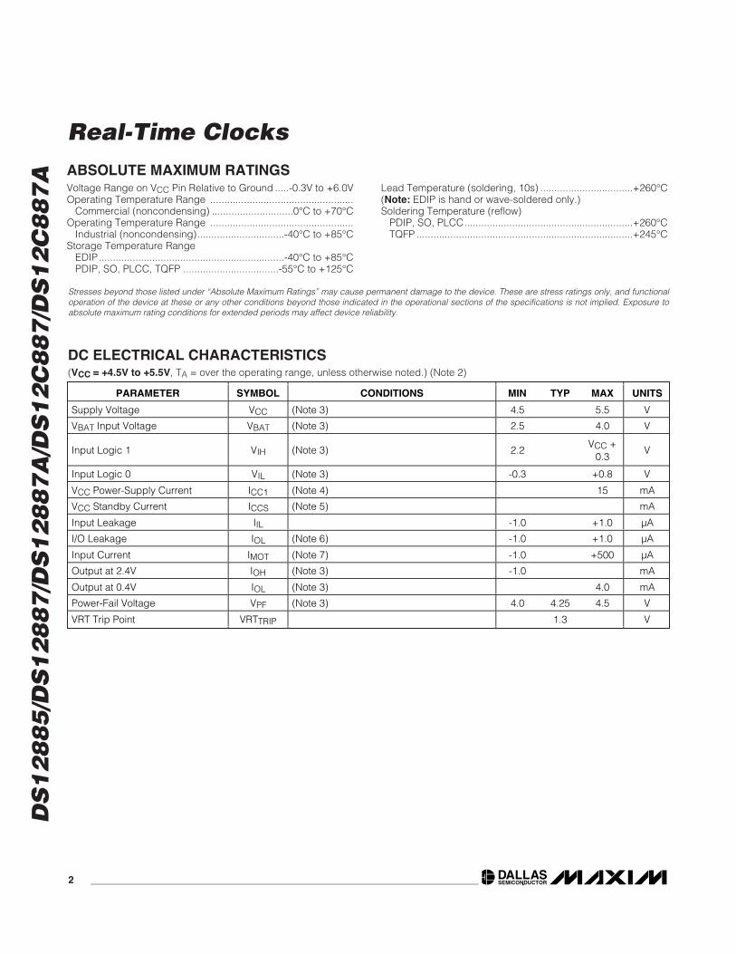
ABSOLUTE MAXIMUM RATINGS
Stresses beyond those listed under “Absolute Maximum Ratings” may cause permanent damage to the device. These are stress ratings only, and functionaloperation of the device at these or any other conditions beyond those indicated in the operational sections of the specifications is not implied. Exposure toabsolute maximum rating conditions for extended periods may affect device reliability.
Voltage Range on VCC Pin Relative to Ground .....-0.3V to +6.0VOperating Temperature Range ...................................................
Commercial (noncondensing) .............................0°C to +70°COperating Temperature Range ...................................................
Industrial (noncondensing)...............................-40°C to +85°CStorage Temperature Range
EDIP..................................................................-40°C to +85°CPDIP, SO, PLCC, TQFP ..................................-55°C to +125°C
Lead Temperature (soldering, 10s) .................................+260°C(Note: EDIP is hand or wave-soldered only.)Soldering Temperature (reflow)
PDIP, SO, PLCC............................................................+260°CTQFP .............................................................................+245°C
DC ELECTRICAL CHARACTERISTICS(VCC = +4.5V to +5.5V, TA = over the operating range, unless otherwise noted.) (Note 2)
PARAMETER SYMBOL CONDITIONS MIN TYP MAX UNITS
Supply Voltage VCC (Note 3) 4.5 5.5 V
VBAT Input Voltage VBAT (Note 3) 2.5 4.0 V
Input Logic 1 VIH (Note 3) 2.2VCC +
0.3V
Input Logic 0 VIL (Note 3) -0.3 +0.8 V
VCC Power-Supply Current ICC1 (Note 4) 15 mA
VCC Standby Current ICCS (Note 5) mA
Input Leakage IIL -1.0 +1.0 µA
I/O Leakage IOL (Note 6) -1.0 +1.0 µA
Input Current IMOT (Note 7) -1.0 +500 µA
Output at 2.4V IOH (Note 3) -1.0 mA
Output at 0.4V IOL (Note 3) 4.0 mA
Power-Fail Voltage VPF (Note 3) 4.0 4.25 4.5 V
VRT Trip Point VRTTRIP 1.3 V
DS
12
88
5/D
S1
28
87
/DS
12
88
7A
/DS
12
C8
87
/DS
12
C8
87
A
Real-Time Clocks
_____________________________________________________________________ 3
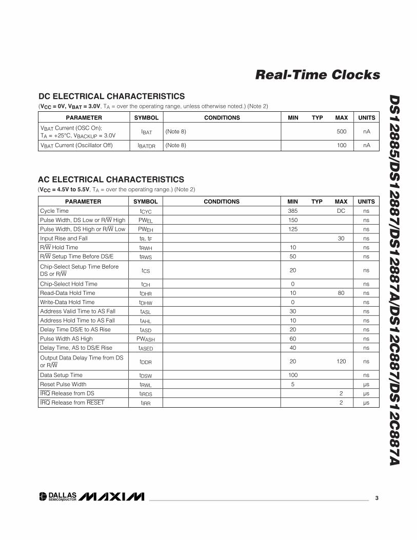
DC ELECTRICAL CHARACTERISTICS(VCC = 0V, VBAT = 3.0V, TA = over the operating range, unless otherwise noted.) (Note 2)
PARAMETER SYMBOL CONDITIONS MIN TYP MAX UNITS
VBAT Current (OSC On);TA = +25°C, VBACKUP = 3.0V
IBAT (Note 8) 500 nA
VBAT Current (Oscillator Off) IBATDR (Note 8) 100 nA
AC ELECTRICAL CHARACTERISTICS(VCC = 4.5V to 5.5V, TA = over the operating range.) (Note 2)
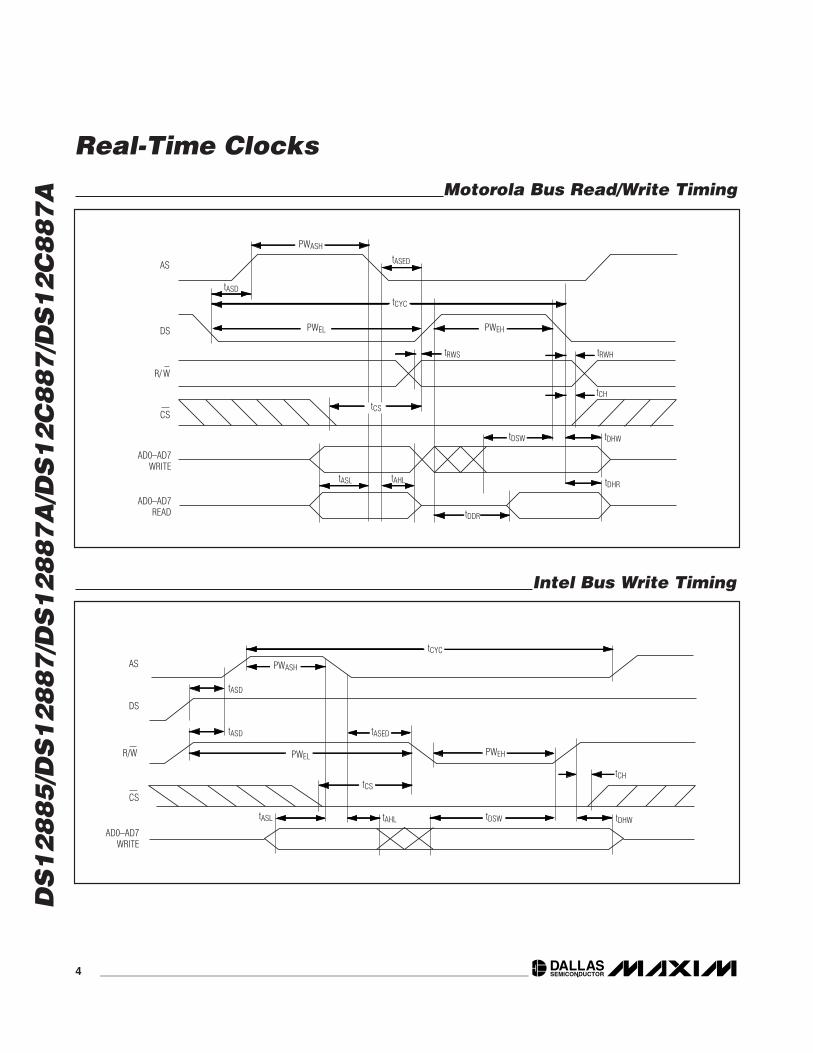
PARAMETER SYMBOL CONDITIONS MIN TYP MAX UNITS
Cycle Time tCYC 385 DC ns
Pulse Width, DS Low or R/W High PWEL 150 ns
Pulse Width, DS High or R/W Low PWEH 125 ns
Input Rise and Fall tR, tF 30 ns
R/W Hold Time tRWH 10 ns
R/W Setup Time Before DS/E tRWS 50 ns
Chip-Select Setup Time BeforeDS or R/W
tCS 20 ns
Chip-Select Hold Time tCH 0 ns
Read-Data Hold Time tDHR 10 80 ns
Write-Data Hold Time tDHW 0 ns
Address Valid Time to AS Fall tASL 30 ns
Address Hold Time to AS Fall tAHL 10 ns
Delay Time DS/E to AS Rise tASD 20 ns
Pulse Width AS High PWASH 60 ns
Delay Time, AS to DS/E Rise tASED 40 ns
Output Data Delay Time from DSor R/W
tDDR 20 120 ns
Data Setup Time tDSW 100 ns
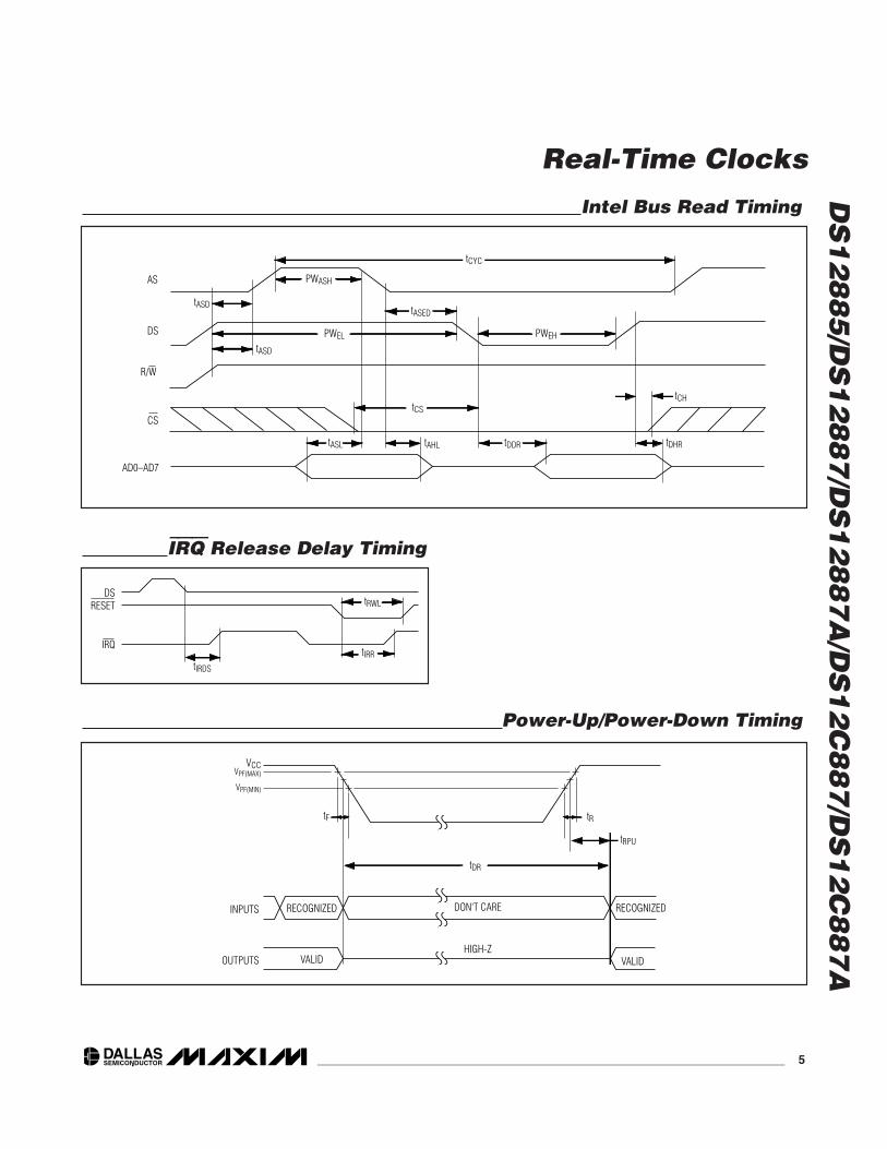
Reset Pulse Width tRWL 5 µs
IRQ Release from DS tIRDS 2 µs
IRQ Release from RESET tIRR 2 µs
DS
12
88
5/D
S1
28
87
/DS
12
88
7A
/DS
12
C8
87
/DS
12
C8
87
A
Real-Time Clocks
4 _____________________________________________________________________
PWASH
PWEL
tASED
tCYC
tRWS
tCS
tRWH
tCH
PWEH
tASD
AD0–AD7READ
CS
R/ W
AS
DS
AD0–AD7WRITE
tDHW
tDHR
tDDR
tAHLtASL
tDSW
Motorola Bus Read/Write Timing
Intel Bus Write Timing
PWASH
PWEL PWEH
tCS
tAHLtASL tDSW tDHW
tCH
tASD
tASD
tCYC
CS
R/W
AS
DS
AD0–AD7WRITE
tASED
DS
12
88
5/D
S1
28
87
/DS
12
88
7A
/DS
12
C8
87
/DS
12
C8
87
A
Real-Time Clocks
_____________________________________________________________________ 5
tCS
tAHLtASL
tCYC
PWASH
PWEL PWEH
CS
R/W
AS
DS
AD0–AD7
tASD
tASD
tASED
tDDR tDHR
tCH
Intel Bus Read Timing
tRWL
tIRRtIRDS
DSRESET
IRQ
IRQ Release Delay Timing
OUTPUTS
INPUTS
HIGH-Z
DON'T CARE
VALID
RECOGNIZED RECOGNIZED
VALID
VCC
tF
VPF(MAX)
VPF(MIN)
tRPU
tR
tDR
Power-Up/Power-Down Timing
DS
12
88
5/D
S1
28
87
/DS
12
88
7A
/DS
12
C8
87
/DS
12
C8
87
A
Real-Time Clocks
6 _____________________________________________________________________
POWER-UP/POWER-DOWN CHARACTERISTICS(TA = -40°C to +85°C) (Note 2)
PARAMETER SYMBOL CONDITIONS MIN TYP MAX UNITS
Recovery at Power-Up tRPU 20 200 ms
VCC Fall Time; VPF(MAX) toVPF(MIN)
tF 300 µs
VCC Rise Time; VPF(MIN) toVPF(MAX)
tR 0 µs
CAPACITANCE(TA = +25°C) (Note 9)
PARAMETER SYMBOL CONDITIONS MIN TYP MAX UNITS
Capacitance on All Input PinsExcept X1 and X2
CIN 5 pF
Capacitance on IRQ, SQW, andDQ Pins
CIO 7 pF
DATA RETENTION(TA = +25°C)
PARAMETER SYMBOL CONDITIONS MIN TYP MAX UNITS
Expected Data Retention tDR 10 years
AC TEST CONDITIONS
PARAMETER TEST CONDITIONS
Input Pulse Levels 0 to 3.0V
Output Load Including Scope and Jig 50pF + 1TTL Gate
Input and Output Timing Measurement Reference Levels Input/Output: VIL maximum and VIH minimum
Input-Pulse Rise and Fall Times 5ns
WARNING: Negative undershoots below -0.3V while the part is in battery-backed mode may cause loss of data.
Note 1: RTC modules can be successfully processed through conventional wave-soldering techniques as long as temperatureexposure to the lithium energy source contained within does not exceed +85°C. However, post-solder cleaning with water-washing techniques is acceptable, provided that ultrasonic vibrations are not used to prevent crystal damage.
Note 2: Limits at -40°C are guaranteed by design and not production tested.Note 3: All voltages are referenced to ground.Note 4: All outputs are open.Note 5: Specified with CS = DS = R/W = RESET = VCC; MOT, AS, AD0–AD7 = 0; VBACKUP open.Note 6: Applies to the AD0 to AD7 pins, the IRQ pin, and the SQW pin when each is in a high-impedance state.Note 7: The MOT pin has an internal 20kΩ pulldown.Note 8: Measured with a 32.768kHz crystal attached to X1 and X2.Note 9: Guaranteed by design. Not production tested.Note 10: Measured with a 50pF capacitance load.
DS
12
88
5/D
S1
28
87
/DS
12
88
7A
/DS
12
C8
87
/DS
12
C8
87
A
Real-Time Clocks
_____________________________________________________________________ 7
Typical Operating Characteristics (VCC = +5.0V, TA = +25°C, unless otherwise noted.)
OSCILLATOR FREQUENCYvs. VCC
DS12
885
toc0
2
VCC (V)FR
EQUE
NCY
(Hz)
5.35.04.8
32768.10
32768.20
32768.30
32768.40
32768.50
32768.60
32768.70
32768.004.5 5.5
IBAT1 vs. VBAT vs. TEMPERATURE
DS12
885
toc0
1
VBAT (V)
I BAT
(nA)
3.82.8 3.0 3.3 3.5
200
300
250
1502.5 4.0
VCC = 0V +85°C
+25°C
0°C
-40°C
+70°C
+40°C
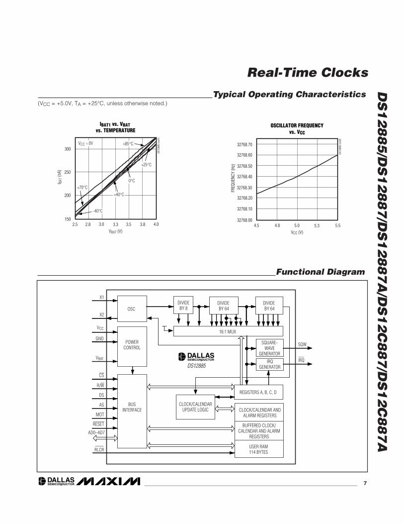
POWERCONTROL
GND
OSC
BUSINTERFACE
VCC
X1
X2
RESET
CS
DS
AS
R/W
MOT
AD0–AD7
DIVIDEBY 8
DIVIDE BY 64
DIVIDE BY 64
16:1 MUX
SQUARE-WAVE
GENERATOR
REGISTERS A, B, C, D
CLOCK/CALENDAR ANDALARM REGISTERS
USER RAM114 BYTES
CLOCK/CALENDARUPDATE LOGIC
IRQ
SQW
IRQGENERATOR
BUFFERED CLOCK/CALENDAR AND ALARM
REGISTERS
VBAT
RLCR
DS12885
Functional Diagram
DS
12
88
5/D
S1
28
87
/DS
12
88
7A
/DS
12
C8
87
/DS
12
C8
87
A
Real-Time Clocks
8 _____________________________________________________________________
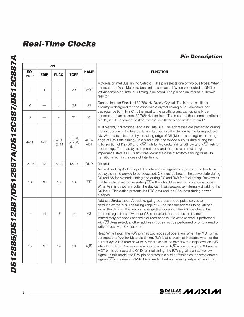
Pin Description
PIN
SO,PDIP EDIP PLCC TQFP
NAME FUNCTION
1 1 2 29 MOT
Motorola or Intel Bus Timing Selector. This pin selects one of two bus types. Whenconnected to VCC, Motorola bus timing is selected. When connected to GND orleft disconnected, Intel bus timing is selected. The pin has an internal pulldownresistor.
2 — 3 30 X1
3 — 4 31 X2
Connections for Standard 32.768kHz Quartz Crystal. The internal oscillatorcircuitry is designed for operation with a crystal having a 6pF specified loadcapacitance (CL). Pin X1 is the input to the oscillator and can optionally beconnected to an external 32.768kHz oscillator. The output of the internal oscillator,pin X2, is left unconnected if an external oscillator is connected to pin X1.
4–11 4–115–10,12, 14
1, 2, 3,5, 7, 8,9, 11
AD0–AD7
Multiplexed, Bidirectional Address/Data Bus. The addresses are presented duringthe first portion of the bus cycle and latched into the device by the falling edge ofAS. Write data is latched by the falling edge of DS (Motorola timing) or the risingedge of R/W (Intel timing). In a read cycle, the device outputs data during thelatter portion of DS (DS and R/W high for Motorola timing, DS low and R/W high forIntel timing). The read cycle is terminated and the bus returns to a high-impedance state as DS transitions low in the case of Motorola timing or as DStransitions high in the case of Intel timing.
12, 16 12 15, 20 12, 17 GND Ground
13 13 16 13 CS
Active-Low Chip-Select Input. The chip-select signal must be asserted low for abus cycle in the device to be accessed. CS must be kept in the active state duringDS and AS for Motorola timing and during DS and R/W for Intel timing. Bus cyclesthat take place without asserting CS will latch addresses, but no access occurs.When VCC is below VPF volts, the device inhibits access by internally disabling theCS input. This action protects the RTC data and the RAM data during poweroutages.
14 14 17 14 AS
Address Strobe Input. A positive-going address-strobe pulse serves todemultiplex the bus. The falling edge of AS causes the address to be latchedwithin the device. The next rising edge that occurs on the AS bus clears theaddress regardless of whether CS is asserted. An address strobe mustimmediately precede each write or read access. If a write or read is performedwith CS deasserted, another address strobe must be performed prior to a read orwrite access with CS asserted.
15 15 19 16 R/W
Read/Write Input. The R/W pin has two modes of operation. When the MOT pin isconnected to VCC for Motorola timing, R/W is at a level that indicates whether thecurrent cycle is a read or write. A read cycle is indicated with a high level on R/Wwhile DS is high. A write cycle is indicated when R/W is low during DS. When theMOT pin is connected to GND for Intel timing, the R/W signal is an active-lowsignal. In this mode, the R/W pin operates in a similar fashion as the write-enablesignal (WE) on generic RAMs. Data are latched on the rising edge of the signal.
DS
12
88
5/D
S1
28
87
/DS
12
88
7A
/DS
12
C8
87
/DS
12
C8
87
A
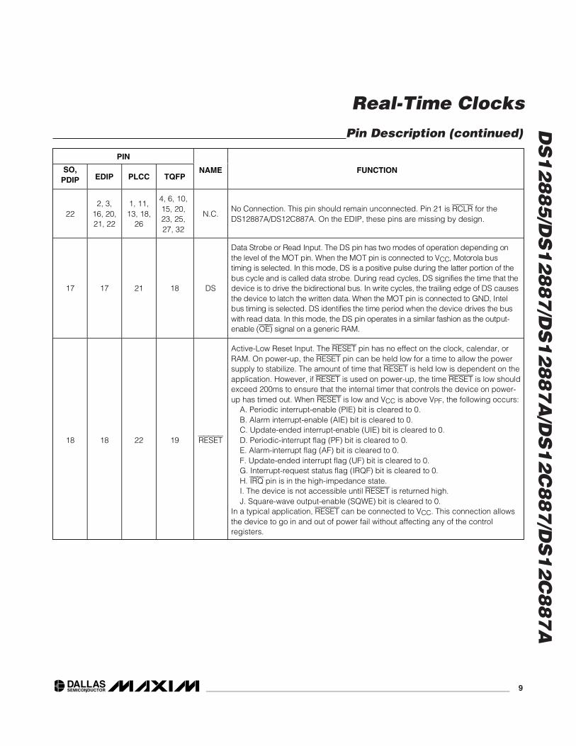
Pin Description (continued)
PIN
SO,PDIP EDIP PLCC TQFP
NAME FUNCTION
222, 3,
16, 20,21, 22
1, 11,13, 18,
26
4, 6, 10,15, 20,23, 25,27, 32
N.C.No Connection. This pin should remain unconnected. Pin 21 is RCLR for theDS12887A/DS12C887A. On the EDIP, these pins are missing by design.
17 17 21 18 DS
D ata S tr ob e or Read Inp ut. The D S p i n has tw o m od es of op er ati on d ep end i ng onthe l evel of the M O T p i n. W hen the M O T p i n i s connected to V C C , M otor ol a b usti m i ng i s sel ected . In thi s m od e, D S i s a p osi ti ve p ul se d ur i ng the l atter p or ti on of theb us cycl e and i s cal l ed d ata str ob e. D ur i ng r ead cycl es, D S si g ni fi es the ti m e that thedevice i s to d r i ve the b i d i r ecti onal b us. In w r i te cycl es, the tr ai l i ng ed g e of D S causesthe device to l atch the w r i tten d ata. W hen the M O T p i n i s connected to GN D , Intel b us ti m i ng i s sel ected . D S i d enti fi es the ti m e p er i od w hen the device d r i ves the b usw i th r ead d ata. In thi s m od e, the D S p i n op er ates i n a si m i l ar fashi on as the outp ut- enab l e ( O E ) si g nal on a g ener i c RAM .
18 18 22 19 RESET
Active-Low Reset Input. The RESET pin has no effect on the clock, calendar, orRAM. On power-up, the RESET pin can be held low for a time to allow the powersupply to stabilize. The amount of time that RESET is held low is dependent on theapplication. However, if RESET is used on power-up, the time RESET is low shouldexceed 200ms to ensure that the internal timer that controls the device on power-up has timed out. When RESET is low and VCC is above VPF, the following occurs: A. Periodic interrupt-enable (PIE) bit is cleared to 0. B. Alarm interrupt-enable (AIE) bit is cleared to 0. C. Update-ended interrupt-enable (UIE) bit is cleared to 0. D. Periodic-interrupt flag (PF) bit is cleared to 0. E. Alarm-interrupt flag (AF) bit is cleared to 0. F. Update-ended interrupt flag (UF) bit is cleared to 0. G. Interrupt-request status flag (IRQF) bit is cleared to 0. H. IRQ pin is in the high-impedance state. I. The device is not accessible until RESET is returned high. J. Square-wave output-enable (SQWE) bit is cleared to 0.In a typical application, RESET can be connected to VCC. This connection allowsthe device to go in and out of power fail without affecting any of the controlregisters.
Real-Time Clocks
_____________________________________________________________________ 9
DS
12
88
5/D
S1
28
87
/DS
12
88
7A
/DS
12
C8
87
/DS
12
C8
87
A
Real-Time Clocks
10 ____________________________________________________________________
Pin Description (continued)
PIN
SO,PDIP EDIP PLCC TQFP
NAME FUNCTION
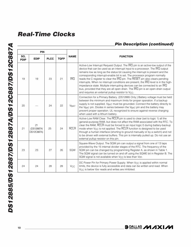
19 19 23 21 IRQ
Active-Low Interrupt Request Output. The IRQ pin is an active-low output of thedevice that can be used as an interrupt input to a processor. The IRQ outputremains low as long as the status bit causing the interrupt is present and thecorresponding interrupt-enable bit is set. The processor program normallyreads the C register to clear the IRQ pin. The RESET pin also clears pendinginterrupts. When no interrupt conditions are present, the IRQ level is in the high-impedance state. Multiple interrupting devices can be connected to an IRQbus, provided that they are all open drain. The IRQ pin is an open-drain outputand requires an external pullup resistor to VCC.
20 — 24 22 VBAT
Connection for a Primary Battery. (DS12885 Only.) Battery voltage must be heldbetween the minimum and maximum limits for proper operation. If a backupsupply is not supplied, VBAT must be grounded. Connect the battery directly tothe VBAT pin. Diodes in series between the VBAT pin and the battery mayprevent proper operation. UL recognized to ensure against reverse chargingwhen used with a lithium battery.
2121
(DS12887A/DS12C887A)
25 24 RCLR
Active-Low RAM Clear. The RCLR pin is used to clear (set to logic 1) all thegeneral-purpose RAM, but does not affect the RAM associated with the RTC. Toclear the RAM, RCLR must be forced to an input logic 0 during battery-backupmode when VCC is not applied. The RCLR function is designed to be usedthrough a human interface (shorting to ground manually or by a switch) and notto be driven with external buffers. This pin is internally pulled up. Do not use anexternal pullup resistor on this pin.
23 23 27 26 SQW
Square-Wave Output. The SQW pin can output a signal from one of 13 tapsprovided by the 15 internal divider stages of the RTC. The frequency of theSQW pin can be changed by programming Register A, as shown in Table 1.The SQW signal can be turned on and off using the SQWE bit in Register B. TheSQW signal is not available when VCC is less than VPF.
24 24 28 28 VCC
DC Power Pin for Primary Power Supply. When VCC is applied within normallimits, the device is fully accessible and data can be written and read. WhenVCC is below VPF reads and writes are inhibited.
DS
12
88
5/D
S1
28
87
/DS
12
88
7A
/DS
12
C8
87
/DS
12
C8
87
A
Real-Time Clocks
____________________________________________________________________ 11
Detailed DescriptionThe DS12885 family of RTCs provide 14 bytes of real-time clock/calendar, alarm, and control/status registersand 114 bytes (113 bytes for DS12C887 andDS12C887A) of nonvolatile, battery-backed static RAM.A time-of-day alarm, three maskable interrupts with acommon interrupt output, and a programmable square-wave output are available. The devices also operate ineither 24-hour or 12-hour format with an AM/PM indica-tor. A precision temperature-compensated circuit moni-tors the status of VCC. If a primary power-supply failureis detected, the devices automatically switch to a back-up supply. The backup supply input supports a primarybattery, such as lithium coin cell. The devices areaccessed through a multiplexed address/data bus thatsupports Intel and Motorola modes.
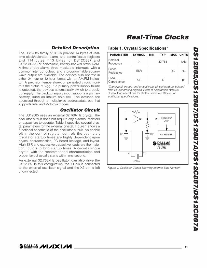
Oscillator CircuitThe DS12885 uses an external 32.768kHz crystal. Theoscillator circuit does not require any external resistorsor capacitors to operate. Table 1 specifies several crys-tal parameters for the external crystal. Figure 1 shows afunctional schematic of the oscillator circuit. An enablebit in the control register controls the oscillator.Oscillator startup times are highly dependent uponcrystal characteristics, PC board leakage, and layout.High ESR and excessive capacitive loads are the majorcontributors to long startup times. A circuit using acrystal with the recommended characteristics andproper layout usually starts within one second.
An external 32.768kHz oscillator can also drive theDS12885. In this configuration, the X1 pin is connectedto the external oscillator signal and the X2 pin is leftunconnected.
COUNTDOWNCHAIN
X1 X2
CRYSTAL
CL1 CL2 RTC REGISTERS
DS12885
Figure 1. Oscillator Circuit Showing Internal Bias Network
PARAMETER SYMBOL MIN TYP MAX UNITS
NominalFrequency
fO 32.768 kHz
SeriesResistance
ESR 50 kΩ
LoadCapacitance
CL 6 pF
Table 1. Crystal Specifications*
*The crystal, traces, and crystal input pins should be isolatedfrom RF generating signals. Refer to Application Note 58:Crystal Considerations for Dallas Real-Time Clocks for additional specifications.
DS
12
88
5/D
S1
28
87
/DS
12
88
7A
/DS
12
C8
87
/DS
12
C8
87
A
Real-Time Clocks
12 ____________________________________________________________________
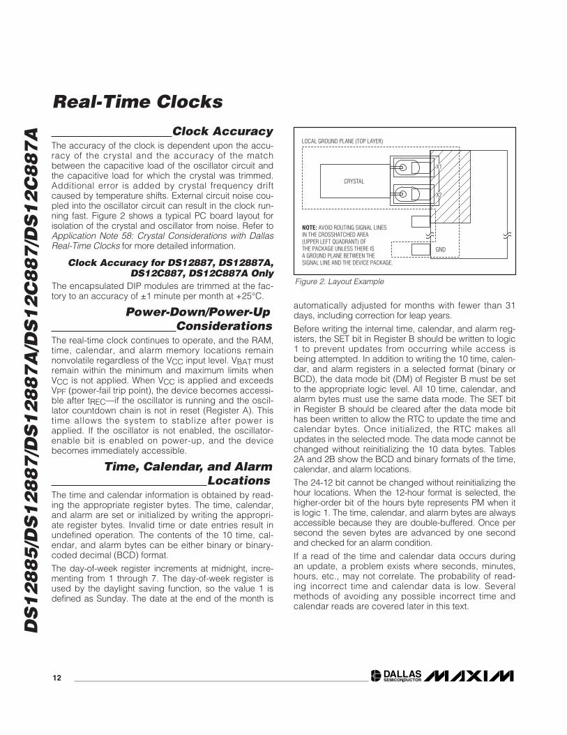
Clock AccuracyThe accuracy of the clock is dependent upon the accu-racy of the crystal and the accuracy of the matchbetween the capacitive load of the oscillator circuit andthe capacitive load for which the crystal was trimmed.Additional error is added by crystal frequency driftcaused by temperature shifts. External circuit noise cou-pled into the oscillator circuit can result in the clock run-ning fast. Figure 2 shows a typical PC board layout forisolation of the crystal and oscillator from noise. Refer toApplication Note 58: Crystal Considerations with DallasReal-Time Clocks for more detailed information.
Clock Accuracy for DS12887, DS12887A,DS12C887, DS12C887A Only
The encapsulated DIP modules are trimmed at the fac-tory to an accuracy of ±1 minute per month at +25°C.
Power-Down/Power-UpConsiderations
The real-time clock continues to operate, and the RAM,time, calendar, and alarm memory locations remainnonvolatile regardless of the VCC input level. VBAT mustremain within the minimum and maximum limits whenVCC is not applied. When VCC is applied and exceedsVPF (power-fail trip point), the device becomes accessi-ble after tREC—if the oscillator is running and the oscil-lator countdown chain is not in reset (Register A). Thistime allows the system to stablize after power isapplied. If the oscillator is not enabled, the oscillator-enable bit is enabled on power-up, and the devicebecomes immediately accessible.
Time, Calendar, and AlarmLocations
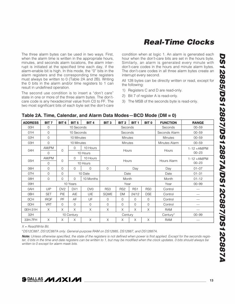
The time and calendar information is obtained by read-ing the appropriate register bytes. The time, calendar,and alarm are set or initialized by writing the appropri-ate register bytes. Invalid time or date entries result inundefined operation. The contents of the 10 time, cal-endar, and alarm bytes can be either binary or binary-coded decimal (BCD) format.
The day-of-week register increments at midnight, incre-menting from 1 through 7. The day-of-week register isused by the daylight saving function, so the value 1 isdefined as Sunday. The date at the end of the month is
automatically adjusted for months with fewer than 31days, including correction for leap years.
Before writing the internal time, calendar, and alarm reg-isters, the SET bit in Register B should be written to logic1 to prevent updates from occurring while access isbeing attempted. In addition to writing the 10 time, calen-dar, and alarm registers in a selected format (binary orBCD), the data mode bit (DM) of Register B must be setto the appropriate logic level. All 10 time, calendar, andalarm bytes must use the same data mode. The SET bitin Register B should be cleared after the data mode bithas been written to allow the RTC to update the time andcalendar bytes. Once initialized, the RTC makes allupdates in the selected mode. The data mode cannot bechanged without reinitializing the 10 data bytes. Tables2A and 2B show the BCD and binary formats of the time,calendar, and alarm locations.
The 24-12 bit cannot be changed without reinitializing thehour locations. When the 12-hour format is selected, thehigher-order bit of the hours byte represents PM when itis logic 1. The time, calendar, and alarm bytes are alwaysaccessible because they are double-buffered. Once persecond the seven bytes are advanced by one secondand checked for an alarm condition.
If a read of the time and calendar data occurs duringan update, a problem exists where seconds, minutes,hours, etc., may not correlate. The probability of read-ing incorrect time and calendar data is low. Severalmethods of avoiding any possible incorrect time andcalendar reads are covered later in this text.
LOCAL GROUND PLANE (TOP LAYER)
CRYSTAL
GND
X2
X1
NOTE: AVOID ROUTING SIGNAL LINES IN THE CROSSHATCHED AREA (UPPER LEFT QUADRANT) OF THE PACKAGE UNLESS THERE IS A GROUND PLANE BETWEEN THE SIGNAL LINE AND THE DEVICE PACKAGE.
Figure 2. Layout Example
DS
12
88
5/D
S1
28
87
/DS
12
88
7A
/DS
12
C8
87
/DS
12
C8
87
A
Real-Time Clocks
____________________________________________________________________ 13
The three alarm bytes can be used in two ways. First,when the alarm time is written in the appropriate hours,minutes, and seconds alarm locations, the alarm inter-rupt is initiated at the specified time each day, if thealarm-enable bit is high. In this mode, the “0” bits in thealarm registers and the corresponding time registersmust always be written to 0 (Table 2A and 2B). Writingthe 0 bits in the alarm and/or time registers to 1 canresult in undefined operation.
The second use condition is to insert a “don’t care”state in one or more of the three alarm bytes. The don’t-care code is any hexadecimal value from C0 to FF. Thetwo most significant bits of each byte set the don’t-care
condition when at logic 1. An alarm is generated eachhour when the don’t-care bits are set in the hours byte.Similarly, an alarm is generated every minute withdon’t-care codes in the hours and minute alarm bytes.The don’t-care codes in all three alarm bytes create aninterrupt every second.
All 128 bytes can be directly written or read, except forthe following:
1) Registers C and D are read-only.
2) Bit 7 of register A is read-only.
3) The MSB of the seconds byte is read-only.
Table 2A. Time, Calendar, and Alarm Data Modes—BCD Mode (DM = 0)
ADDRESS BIT 7 BIT 6 BIT 5 BIT 4 BIT 3 BIT 2 BIT 1 BIT 0 FUNCTION RANGE00H 0 10 Seconds Seconds Seconds 00–59
01H 0 10 Seconds Seconds Seconds Alarm 00–59
02H 0 10 Minutes Minutes Minutes 00–59
03H 0 10 Minutes Minutes Minutes Alarm 00–59
AM/PM 0 10 Hours04H
00
10 HoursHours Hours
1–12 +AM/PM00–23
AM/PM 0 10 Hours05H
00
10 HoursHours Hours Alarm
1–12 +AM/PM00–23
06H 0 0 0 0 0 Day Day 01–07
07H 0 0 10 Date Date Date 01–31
08H 0 0 0 10 Months Month Month 01–12
09H 10 Years Year Year 00–99
0AH UIP DV2 DV1 DV0 RS3 RS2 RS1 RS0 Control —
0BH SET PIE AIE UIE SQWE DM 24/12 DSE Control —
0CH IRQF PF AF UF 0 0 0 0 Control —
0DH VRT 0 0 0 0 0 0 0 Control —
0EH-31H X X X X X X X X RAM —
32H 10 Century Century Century* 00–99
33H-7FH X X X X X X X X RAM —
X = Read/Write Bit.*DS12C887, DS12C887A only. General-purpose RAM on DS12885, DS12887, and DS12887A.
Note: Unless otherwise specified, the state of the registers is not defined when power is first applied. Except for the seconds regis-ter, 0 bits in the time and date registers can be written to 1, but may be modified when the clock updates. 0 bits should always bewritten to 0 except for alarm mask bits.
DS
12
88
5/D
S1
28
87
/DS
12
88
7A
/DS
12
C8
87
/DS
12
C8
87
A
Real-Time Clocks
14 ____________________________________________________________________
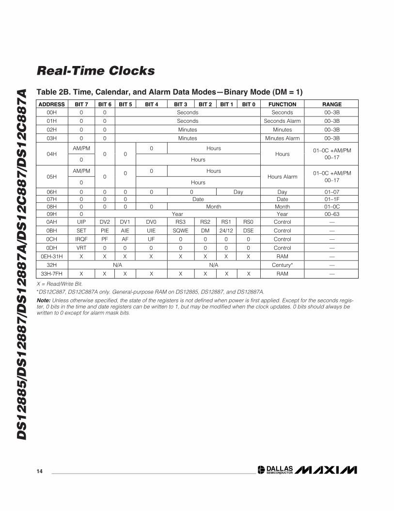
Table 2B. Time, Calendar, and Alarm Data Modes—Binary Mode (DM = 1)
ADDRESS BIT 7 BIT 6 BIT 5 BIT 4 BIT 3 BIT 2 BIT 1 BIT 0 FUNCTION RANGE00H 0 0 Seconds Seconds 00–3B
01H 0 0 Seconds Seconds Alarm 00–3B
02H 0 0 Minutes Minutes 00–3B
03H 0 0 Minutes Minutes Alarm 00–3B
AM/PM 0 Hours04H
00 0
HoursHours
01–0C +AM/PM00–17
AM/PM 0 Hours05H
00
0
HoursHours Alarm
01–0C +AM/PM00–17
06H 0 0 0 0 0 Day Day 01–0707H 0 0 0 Date Date 01–1F08H 0 0 0 0 Month Month 01–0C09H 0 Year Year 00–630AH UIP DV2 DV1 DV0 RS3 RS2 RS1 RS0 Control —
0BH SET PIE AIE UIE SQWE DM 24/12 DSE Control —
0CH IRQF PF AF UF 0 0 0 0 Control —
0DH VRT 0 0 0 0 0 0 0 Control —
0EH-31H X X X X X X X X RAM —
32H N/A N/A Century* —
33H-7FH X X X X X X X X RAM —
X = Read/Write Bit.*DS12C887, DS12C887A only. General-purpose RAM on DS12885, DS12887, and DS12887A.
Note: Unless otherwise specified, the state of the registers is not defined when power is first applied. Except for the seconds regis-ter, 0 bits in the time and date registers can be written to 1, but may be modified when the clock updates. 0 bits should always bewritten to 0 except for alarm mask bits.
DS
12
88
5/D
S1
28
87
/DS
12
88
7A
/DS
12
C8
87
/DS
12
C8
87
A
Real-Time Clocks
____________________________________________________________________ 15
Bit 7: Update-In-Progress (UIP). This bit is a statusflag that can be monitored. When the UIP bit is a 1, theupdate transfer occurs soon. When UIP is a 0, theupdate transfer does not occur for at least 244µs. Thetime, calendar, and alarm information in RAM is fullyavailable for access when the UIP bit is 0. The UIP bit isread-only and is not affected by RESET. Writing theSET bit in Register B to a 1 inhibits any update transferand clears the UIP status bit.
Bits 6, 5, and 4: DV2, DV1, DV0. These three bits areused to turn the oscillator on or off and to reset thecountdown chain. A pattern of 010 is the only combina-tion of bits that turn the oscillator on and allow the RTCto keep time. A pattern of 11x enables the oscillator butholds the countdown chain in reset. The next updateoccurs at 500ms after a pattern of 010 is written to DV0,DV1, and DV2.
Bits 3 to 0: Rate Selector (RS3, RS2, RS1, RS0).These four rate-selection bits select one of the 13 tapson the 15-stage divider or disable the divider output.The tap selected can be used to generate an outputsquare wave (SQW pin) and/or a periodic interrupt. Theuser can do one of the following:
1) Enable the interrupt with the PIE bit;
2) Enable the SQW output pin with the SQWE bit;
3) Enable both at the same time and the same rate;or
4) Enable neither.
Table 3 lists the periodic interrupt rates and the square-wave frequencies that can be chosen with the RS bits.These four read/write bits are not affected by RESET.
BIT 7 BIT 6 BIT 5 BIT 4 BIT 3 BIT 2 BIT 1 BIT 0
UIP DV2 DV1 DV0 RS3 RS2 RS1 RS0
Control Register A
Control RegistersThe real-time clocks have four control registers that areaccessible at all times, even during the update cycle.
MSB LSB
DS
12
88
5/D
S1
28
87
/DS
12
88
7A
/DS
12
C8
87
/DS
12
C8
87
A
Real-Time Clocks
16 ____________________________________________________________________
Bit 7: SET. When the SET bit is 0, the update transferfunctions normally by advancing the counts once persecond. When the SET bit is written to 1, any updatetransfer is inhibited, and the program can initialize thetime and calendar bytes without an update occurring inthe midst of initializing. Read cycles can be executed ina similar manner. SET is a read/write bit and is notaffected by RESET or internal functions of the device.
Bit 6: Periodic Interrupt Enable (PIE). The PIE bit is aread/write bit that allows the periodic interrupt flag (PF) bitin Register C to drive the IRQ pin low. When the PIE bit isset to 1, periodic interrupts are generated by driving theIRQ pin low at a rate specified by the RS3–RS0 bits ofRegister A. A 0 in the PIE bit blocks the IRQ output frombeing driven by a periodic interrupt, but the PF bit is stillset at the periodic rate. PIE is not modified by any internaldevice functions, but is cleared to 0 on RESET.
Bit 5: Alarm Interrupt Enable (AIE). This bit is aread/write bit that, when set to 1, permits the alarm flag(AF) bit in Register C to assert IRQ. An alarm interruptoccurs for each second that the three time bytes equalthe three alarm bytes, including a don’t-care alarmcode of binary 11XXXXXX. The AF bit does not initiatethe IRQ signal when the AIE bit is set to 0. The internalfunctions of the device do not affect the AIE bit, but iscleared to 0 on RESET.
Bit 4: Update-Ended Interrupt Enable (UIE). This bit isa read/write bit that enables the update-end flag (UF)bit in Register C to assert IRQ. The RESET pin goinglow or the SET bit going high clears the UIE bit.
The internal functions of the device do not affect theUIE bit, but is cleared to 0 on RESET.
Bit 3: Square-Wave Enable (SQWE). When this bit isset to 1, a square-wave signal at the frequency set bythe rate-selection bits RS3–RS0 is driven out on the SQWpin. When the SQWE bit is set to 0, the SQW pin is heldlow. SQWE is a read/write bit and is cleared by RESET.SQWE is low if disabled, and is high impedance whenVCC is below VPF. SQWE is cleared to 0 on RESET.
Bit 2: Data Mode (DM). This bit indicates whether timeand calendar information is in binary or BCD format.The DM bit is set by the program to the appropriate for-mat and can be read as required. This bit is not modi-fied by internal functions or RESET. A 1 in DM signifiesbinary data, while a 0 in DM specifies BCD data.
Bit 1: 24/12. The 24/12 control bit establishes the for-mat of the hours byte. A 1 indicates the 24-hour modeand a 0 indicates the 12-hour mode. This bit isread/write and is not affected by internal functions orRESET.
Bit 0: Daylight Saving Enable (DSE). This bit is aread/write bit that enables two daylight saving adjust-ments when DSE is set to 1. On the first Sunday inApril, the time increments from 1:59:59 AM to 3:00:00AM. On the last Sunday in October when the time firstreaches 1:59:59 AM, it changes to 1:00:00 AM. WhenDSE is enabled, the internal logic test for the first/lastSunday condition at midnight. If the DSE bit is not setwhen the test occurs, the daylight saving function doesnot operate correctly. These adjustments do not occurwhen the DSE bit is 0. This bit is not affected by internalfunctions or RESET.
BIT 7 BIT 6 BIT 5 BIT 4 BIT 3 BIT 2 BIT 1 BIT 0
SET PIE AIE UIE SQWE DM 24/12 DSE
Control Register B
MSB LSB
DS
12
88
5/D
S1
28
87
/DS
12
88
7A
/DS
12
C8
87
/DS
12
C8
87
A
Real-Time Clocks
____________________________________________________________________ 17
Bit 7: Interrupt Request Flag (IRQF). This bit is set to1 when any of the following are true:
PF = PIE = 1
AF = AIE = 1
UF = UIE = 1
Any time the IRQF bit is 1, the IRQ pin is driven low.This bit can be cleared by reading Register C or with aRESET.
Bit 6: Periodic Interrupt Flag (PF). This bit is read-only and is set to 1 when an edge is detected on theselected tap of the divider chain. The RS3 through RS0bits establish the periodic rate. PF is set to 1 indepen-dent of the state of the PIE bit. When both PF and PIEare 1s, the IRQ signal is active and sets the IRQF bit.This bit can be cleared by reading Register C or with aRESET.
Bit 5: Alarm Interrupt Flag (AF). A 1 in the AF bit indi-cates that the current time has matched the alarm time.If the AIE bit is also 1, the IRQ pin goes low and a 1appears in the IRQF bit. This bit can be cleared byreading Register C or with a RESET.
Bit 5: Update-Ended Interrupt Flag (UF). This bit isset after each update cycle. When the UIE bit is set to1, the 1 in UF causes the IRQF bit to be a 1, whichasserts the IRQ pin. This bit can be cleared by readingRegister C or with a RESET.
Bits 3 to 0: Unused. These bits are unused in RegisterC. These bits always read 0 and cannot be written.
BIT 7 BIT 6 BIT 5 BIT 4 BIT 3 BIT 2 BIT 1 BIT 0
IRQF PF AF UF 0 0 0 0
Control Register C
BIT 7 BIT 6 BIT 5 BIT 4 BIT 3 BIT 2 BIT 1 BIT 0VRT 0 0 0 0 0 0 0
Control Register D
Bit 7: Valid RAM and Time (VRT). This bit indicatesthe condition of the battery connected to the VBAT pin.This bit is not writeable and should always be 1 whenread. If a 0 is ever present, an exhausted internal lithi-um energy source is indicated and both the contents of
the RTC data and RAM data are questionable. This bitis unaffected by RESET.
Bits 6 to 0: Unused. The remaining bits of Register Dare not usable. They cannot be written and they alwaysread 0.
MSB LSB
MSB LSB
DS
12
88
5/D
S1
28
87
/DS
12
88
7A
/DS
12
C8
87
/DS
12
C8
87
A
Real-Time Clocks
18 ____________________________________________________________________
Century Register(DS12C887/DS12C887A Only)
The century register at location 32h is a BCD registerdesigned to automatically load the BCD value 20 as theyear register changes from 99 to 00. The MSB of thisregister is not affected when the load of 20 occurs, andremains at the value written by the user.
Nonvolatile RAM (NV RAM)The general-purpose NV RAM bytes are not dedicatedto any special function within the device. They can beused by the processor program as battery-backedmemory and are fully available during the update cycle.
InterruptsThe RTC family includes three separate, fully automaticsources of interrupt for a processor. The alarm interruptcan be programmed to occur at rates from once persecond to once per day. The periodic interrupt can beselected for rates from 500ms to 122µs. The update-ended interrupt can be used to indicate to the programthat an update cycle is complete. Each of these inde-pendent interrupt conditions is described in greaterdetail in other sections of this text.
The processor program can select which interrupts, ifany, are to be used. Three bits in Register B enable theinterrupts. Writing a logic 1 to an interrupt-enable bitpermits that interrupt to be initiated when the eventoccurs. A 0 in an interrupt-enable bit prohibits the IRQpin from being asserted from that interrupt condition. Ifan interrupt flag is already set when an interrupt isenabled, IRQ is immediately set at an active level,although the interrupt initiating the event may haveoccurred earlier. As a result, there are cases where theprogram should clear such earlier initiated interruptsbefore first enabling new interrupts.
When an interrupt event occurs, the relating flag bit isset to logic 1 in Register C. These flag bits are set inde-pendent of the state of the corresponding enable bit inRegister B. The flag bit can be used in a polling modewithout enabling the corresponding enable bits. Theinterrupt flag bit is a status bit that software can interro-gate as necessary. When a flag is set, an indication isgiven to software that an interrupt event has occurredsince the flag bit was last read; however, care shouldbe taken when using the flag bits as they are clearedeach time Register C is read. Double latching is includ-ed with Register C so that bits that are set remain sta-ble throughout the read cycle. All bits that are set (high)are cleared when read, and new interrupts that arepending during the read cycle are held until after thecycle is completed. One, two, or three bits can be set
when reading Register C. Each used flag bit should beexamined when Register C is read to ensure that nointerrupts are lost.
The second flag bit method is used with fully enabledinterrupts. When an interrupt flag bit is set and the cor-responding interrupt-enable bit is also set, the IRQ pin isasserted low. IRQ is asserted as long as at least one ofthe three interrupt sources has its flag and enable bitsset. The IRQF bit in Register C is a 1 whenever the IRQpin is driven low. Determination that the RTC initiated aninterrupt is accomplished by reading Register C. A logic1 in bit 7 (IRQF bit) indicates that one or more interruptshave been initiated by the device. The act of readingRegister C clears all active flag bits and the IRQF bit.
Oscillator Control BitsWhen the DS12887, DS12887A, DS12C887, andDS12C887A are shipped from the factory, the internaloscillator is turned off. This prevents the lithium energycell from being used until the device is installed in asystem.
A pattern of 010 in bits 4 to 6 of Register A turns theoscillator on and enables the countdown chain. A pat-tern of 11x (DV2 = 1, DV1 = 1, DV0 = X) turns the oscil-lator on, but holds the countdown chain of the oscillatorin reset. All other combinations of bits 4 to 6 keep theoscillator off.
Square-Wave Output SelectionThirteen of the 15 divider taps are made available to a 1-of-16 multiplexer, as shown in the functional diagram.The square-wave and periodic-interrupt generatorsshare the output of the multiplexer. The RS0–RS3 bits inRegister A establish the output frequency of the multi-plexer (see Table 1). Once the frequency is selected, theoutput of the SQW pin can be turned on and off underprogram control with the square-wave enable bit, SQWE.
Periodic Interrupt SelectionThe periodic interrupt causes the IRQ pin to go to anactive state from once every 500ms to once every 122µs.This function is separate from the alarm interrupt, whichcan be output from once per second to once per day.The periodic interrupt rate is selected using the sameRegister A bits that select the square-wave frequency(Table 1). Changing the Register A bits affects thesquare-wave frequency and the periodic-interrupt out-put. However, each function has a separate enable bit inRegister B. The SQWE bit controls the square-wave out-put. Similarly, the PIE bit in Register B enables the peri-odic interrupt. The periodic interrupt can be used withsoftware counters to measure inputs, create output inter-vals, or await the next needed software function.
DS
12
88
5/D
S1
28
87
/DS
12
88
7A
/DS
12
C8
87
/DS
12
C8
87
A
Real-Time Clocks
____________________________________________________________________ 19
Update CycleThe device executes an update cycle once per secondregardless of the SET bit in Register B. When the SETbit in Register B is set to 1, the user copy of the double-buffered time, calendar, and alarm bytes is frozen anddoes not update as the time increments. However, thetime countdown chain continues to update the internalcopy of the buffer. This feature allows time to maintainaccuracy independent of reading or writing the time,calendar, and alarm buffers, and also guarantees thattime and calendar information is consistent. The updatecycle also compares each alarm byte with the corre-
sponding time byte and issues an alarm if a match or ifa don’t-care code is present in all three positions.
There are three methods that can handle RTC accessthat avoid any possibility of accessing inconsistent timeand calendar data. The first method uses the update-ended interrupt. If enabled, an interrupt occurs afterevery update cycle that indicates over 999ms is avail-able to read valid time and date information. If thisinterrupt is used, the IRQF bit in Register C should becleared before leaving the interrupt routine.
A second method uses the update-in-progress bit (UIP)in Register A to determine if the update cycle is inprogress. The UIP bit pulses once per second. Afterthe UIP bit goes high, the update transfer occurs 244µslater. If a low is read on the UIP bit, the user has at least244µs before the time/calendar data is changed.Therefore, the user should avoid interrupt service rou-tines that would cause the time needed to read validtime/calendar data to exceed 244µs.
The third method uses a periodic interrupt to determine ifan update cycle is in progress. The UIP bit in Register Ais set high between the setting of the PF bit in Register C(Figure 3). Periodic interrupts that occur at a rate greaterthan tBUC allow valid time and date information to bereached at each occurrence of the periodic interrupt.The reads should be complete within one (tPI/2 + tBUC)to ensure that data is not read during the update cycle.
Handling, PC Board Layout,and Assembly
The EDIP module can be successfully processedthrough conventional wave-soldering techniques so longas temperature exposure to the lithium energy sourcedoes not exceed +85°C. Post-solder cleaning with water-washing techniques is acceptable, provided that ultra-sonic vibration is not used. Such cleaning can damagethe crystal.
SELECT BITSREGISTER A
RS3 RS2 RS1 RS0
tPI PERIODICINTERRUPT
RATE
SQW OUTPUTFREQUENCY
0 0 0 0 None None
0 0 0 1 3.90625ms 256Hz
0 0 1 0 7.8125ms 128Hz
0 0 1 1 122.070µs 8.192kHz
0 1 0 0 244.141µs 4.096kHz
0 1 0 1 488.281µs 2.048kHz
0 1 1 0 976.5625µs 1.024kHz
0 1 1 1 1.953125ms 512Hz
1 0 0 0 3.90625ms 256Hz
1 0 0 1 7.8125ms 128Hz
1 0 1 0 15.625ms 64Hz
1 0 1 1 31.25ms 32Hz
1 1 0 0 62.5ms 16Hz
1 1 0 1 125ms 8Hz
1 1 1 0 250ms 4Hz
1 1 1 1 500ms 2Hz
Table 3. Periodic Interrupt Rate andSquare-Wave Output Frequency
UIP
UF
PF
tBUC = DELAY TIME BEFORE UPDATECYCLE = 244μs
1 SECOND
t PI
tP1/2 tP1/2
tBUC
Figure 3. UIP and Periodic Interrupt Timing
DS
12
88
5/D
S1
28
87
/DS
12
88
7A
/DS
12
C8
87
/DS
12
C8
87
A
Real-Time Clocks
20 ____________________________________________________________________
24
23
22
21
20
19
18
17
1
2
3
4
5
6
7
8
VCC
SQW
N.C.
RCLRAD0
X2
X1
MOT
TOP VIEW
VBAT
IRQ
RESET
DSAD4
AD3
AD2
AD1
16
15
14
13
9
10
11
12
GND
R/W
AS
CSGND
AD7
AD6
AD5
SO, PDIP
PLCC
DS12885DS12885S
DS12885Q
VCC
SQW
N.C.
N.C.(RCLR)
AD0
N.C.
N.C.
MOT
N.C.
IRQ
RESET
DSAD4
AD3
AD2
AD1
N.C.
R/W
AS
CS
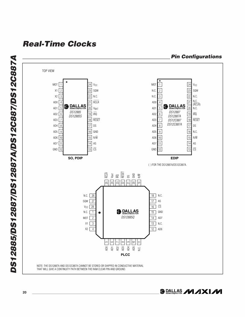
( ) FOR THE DS12887A/DS12C887A.
NOTE: THE DS12887A AND DS12C887A CANNOT BE STORED OR SHIPPED IN CONDUCTIVE MATERIAL THAT WILL GIVE A CONTINUITY PATH BETWEEN THE RAM CLEAR PIN AND GROUND.
GND
AD7
AD6
AD5
EDIP
DS12887DS12887ADS12C887
DS12C887A
12
13
14
15
16
17
18
1N.C.
VCC
SQW
N.C.
MOT
X1
X2
GND
CS
AS
N.C.
AD7
N.C.
AD6
2
3
4
26
27
28
192021222324255 6 7 8 9 10 11
AD0
AD1
AD2
AD3
AD4
AD5
N.C.
RCLR
V BAT
IRQ
RESE
T
DS GND
R/W
1
2
3
4
5
6
7
8
9
10
11
12
24
23
22
21
20
19
18
17
16
15
14
13
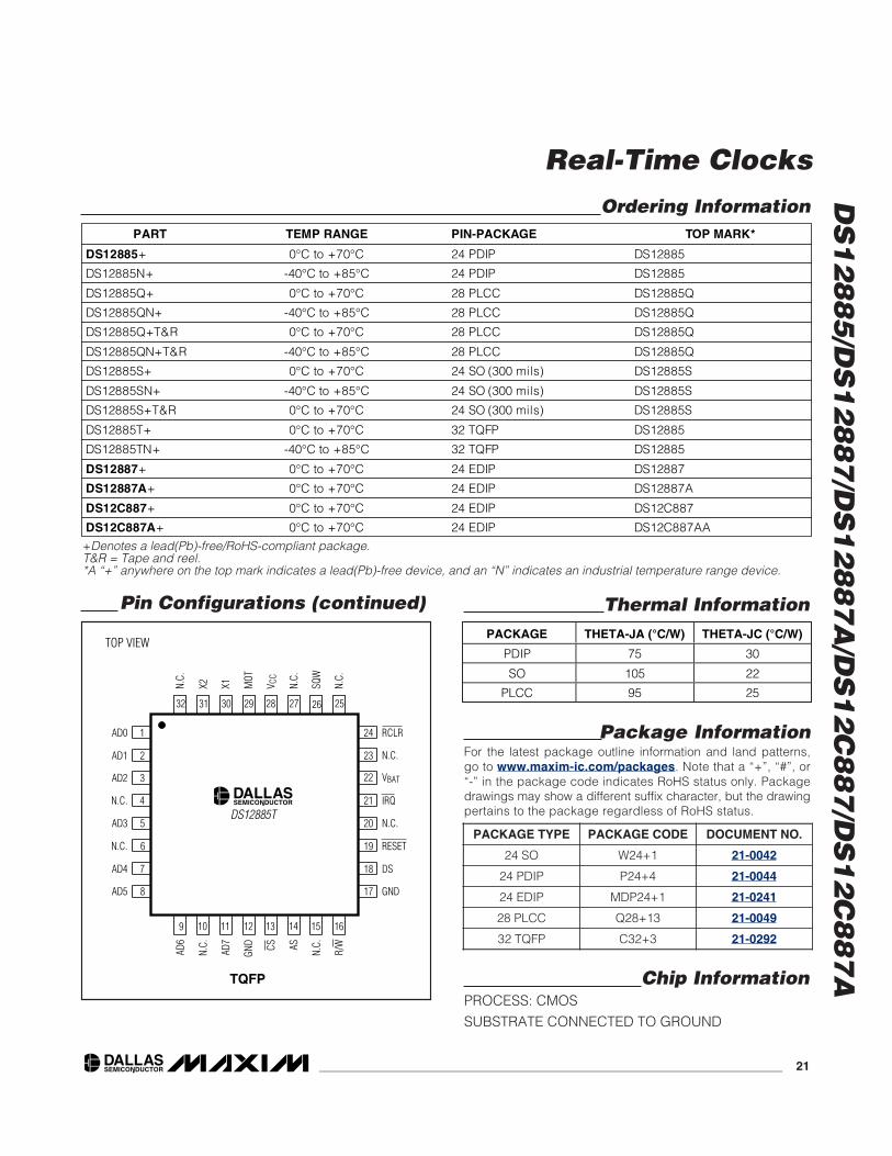
Pin Configurations
DS
12
88
5/D
S1
28
87
/DS
12
88
7A
/DS
12
C8
87
/DS
12
C8
87
A
Real-Time Clocks
____________________________________________________________________ 21
PACKAGE THETA-JA (°C/W) THETA-JC (°C/W)
PDIP 75 30
SO 105 22
PLCC 95 25
Thermal Information
Chip InformationPROCESS: CMOS
SUBSTRATE CONNECTED TO GROUND
TQFP
TOP VIEW
32 28293031 252627
X2 X1 MOT
V CC
N.C.
N.C.
SQW
N.C.
10 13 1514 1611 129
AD6
AD7
N.C. CSGND
N.C.AS R/W
17
18
19
20
21
22
23 N.C.
24 RCLR
VBAT
IRQ
N.C.
RESET
DS
GND
2
3
4
5
6
7
8AD5
AD4
N.C.
AD3
N.C.
AD2
AD1
1AD0
DS12885T
Pin Configurations (continued)
Ordering InformationPART TEMP RANGE PIN-PACKAGE TOP MARK*
DS12885+ 0°C to +70°C 24 PDIP DS12885
DS12885N+ -40°C to +85°C 24 PDIP DS12885
DS12885Q+ 0°C to +70°C 28 PLCC DS12885Q
DS12885QN+ -40°C to +85°C 28 PLCC DS12885Q
DS12885Q+T&R 0°C to +70°C 28 PLCC DS12885Q
DS12885QN+T&R -40°C to +85°C 28 PLCC DS12885Q
DS12885S+ 0°C to +70°C 24 SO (300 mils) DS12885S
DS12885SN+ -40°C to +85°C 24 SO (300 mils) DS12885S
DS12885S+T&R 0°C to +70°C 24 SO (300 mils) DS12885S
DS12885T+ 0°C to +70°C 32 TQFP DS12885
DS12885TN+ -40°C to +85°C 32 TQFP DS12885
DS12887+ 0°C to +70°C 24 EDIP DS12887
DS12887A+ 0°C to +70°C 24 EDIP DS12887A
DS12C887+ 0°C to +70°C 24 EDIP DS12C887
DS12C887A+ 0°C to +70°C 24 EDIP DS12C887AA
+Denotes a lead(Pb)-free/RoHS-compliant package.T&R = Tape and reel.*A “+” anywhere on the top mark indicates a lead(Pb)-free device, and an “N” indicates an industrial temperature range device.
PACKAGE TYPE PACKAGE CODE DOCUMENT NO.
24 SO W24+1 21-0042
24 PDIP P24+4 21-0044
24 EDIP MDP24+1 21-0241
28 PLCC Q28+13 21-0049
32 TQFP C32+3 21-0292
Package InformationFor the latest package outline information and land patterns,go to www.maxim-ic.com/packages. Note that a “+”, “#”, or“-” in the package code indicates RoHS status only. Packagedrawings may show a different suffix character, but the drawingpertains to the package regardless of RoHS status.
DS
12
88
5/D
S1
28
87
/DS
12
88
7A
/DS
12
C8
87
/DS
12
C8
87
A
Real-Time Clocks
Maxim cannot assume responsibility for use of any circuitry other than circuitry entirely embodied in a Maxim product. No circuit patent licenses areimplied. Maxim reserves the right to change the circuitry and specifications without notice at any time.
22 ____________________Maxim Integrated Products, 120 San Gabriel Drive, Sunnyvale, CA 94086 408-737-7600
© 2010 Maxim Integrated Products Maxim is a registered trademark of Maxim Integrated Products, Inc.
is a registered trademark of Maxim Integrated Products, Inc.
Quijano
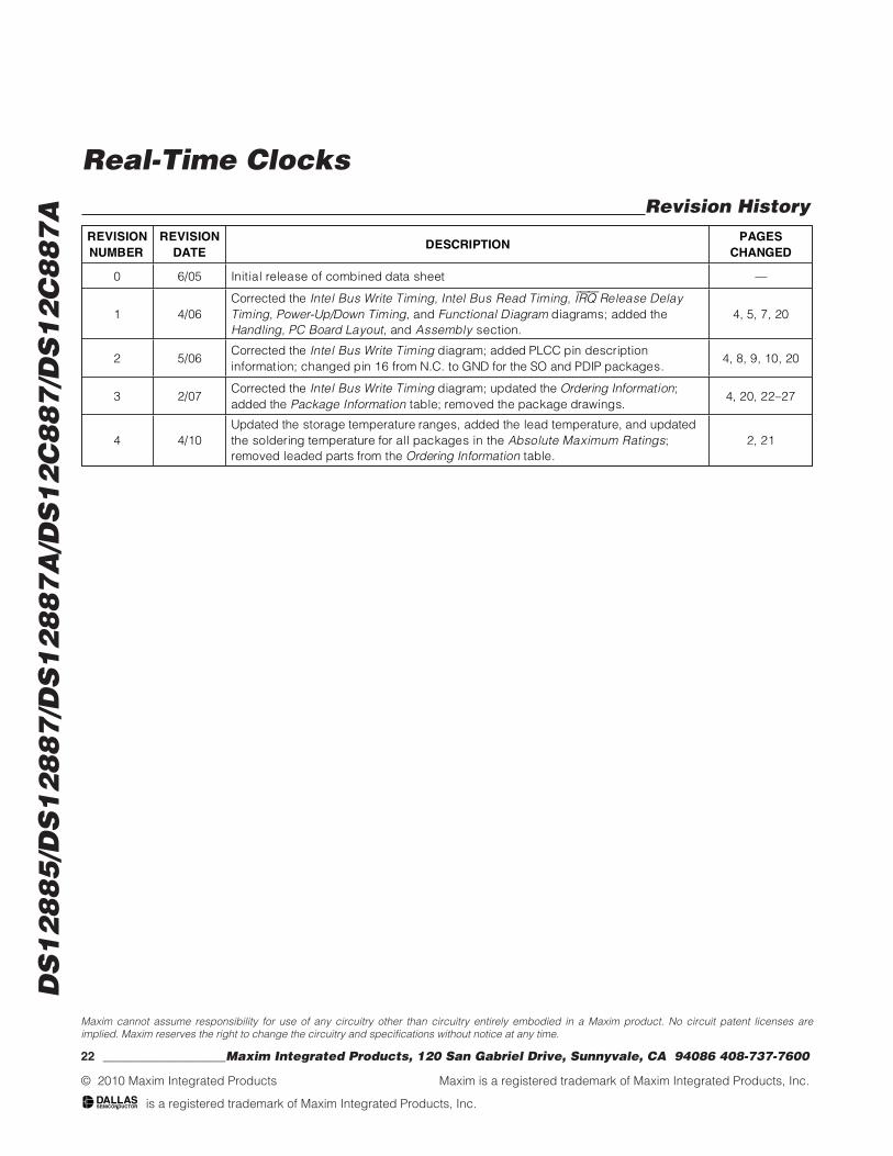
Revision HistoryREVISION NUMBER
REVISION DATE
DESCRIPTIONPAGES
CHANGED
0 6/05 Initial release of combined data sheet —
1 4/06 Corrected the Intel Bus Write Timing, Intel Bus Read Timing, IRQ Release Delay Timing, Power-Up/Down Timing, and Functional Diagram diagrams; added the Handling, PC Board Layout, and Assembly section.
4, 5, 7, 20
2 5/06 Corrected the Intel Bus Write Timing diagram; added PLCC pin description information; changed pin 16 from N.C. to GND for the SO and PDIP packages.
4, 8, 9, 10, 20
3 2/07 Corrected the Intel Bus Write Timing diagram; updated the Ordering Information;added the Package Information table; removed the package drawings.
4, 20, 22–27
4 4/10 Updated the storage temperature ranges, added the lead temperature, and updated the soldering temperature for all packages in the Absolute Maximum Ratings;removed leaded parts from the Ordering Information table.
2, 21