Embed Size (px)
Citation preview

Lecture 300 – Buffered Op Amps (3/21/02) Page 300-1
ECE 6412 - Analog Integrated Circuit Design - II © P.E. Allen - 2002
LECTURE 300 – BUFFERED OP AMPS(READING: AH – 352-368)
ObjectiveThe objective of this presentation is:1.) Illustrate the method of lowering the output resistance of simple op amps2.) Show examplesOutline• Open-loop, MOSFET buffered op amps• Closed-loop MOSFET buffered op amps• BJT output op amps• SummaryGoalTo illustrate the degrees of freedom andchoices of different circuit architecturesthat can enhance the performance of agiven op amp.
Two-StageOp Amp
BufferedHigh FrequencyDifferential
Output
Low Power Low Noise
Low Voltage Fig. 7.0-1
Lecture 300 – Buffered Op Amps (3/21/02) Page 300-2
ECE 6412 - Analog Integrated Circuit Design - II © P.E. Allen - 2002
What is a Buffered Op Amp?A buffered op amp is an op amp with a low value of output resistance, Ro.
Typically, 10Ω ≤ Ro ≤ 1000Ω
RequirementsGenerally the same as for the output amplifier:• Low output resistance• Large output signal swing• Low distortion• High efficiencyTypes of Buffered Op Amps• Buffered op amps using MOSFETs
With and without negative feedback• Buffered op amps using BJTs
Lecture 300 – Buffered Op Amps (3/21/02) Page 300-3
ECE 6412 - Analog Integrated Circuit Design - II © P.E. Allen - 2002
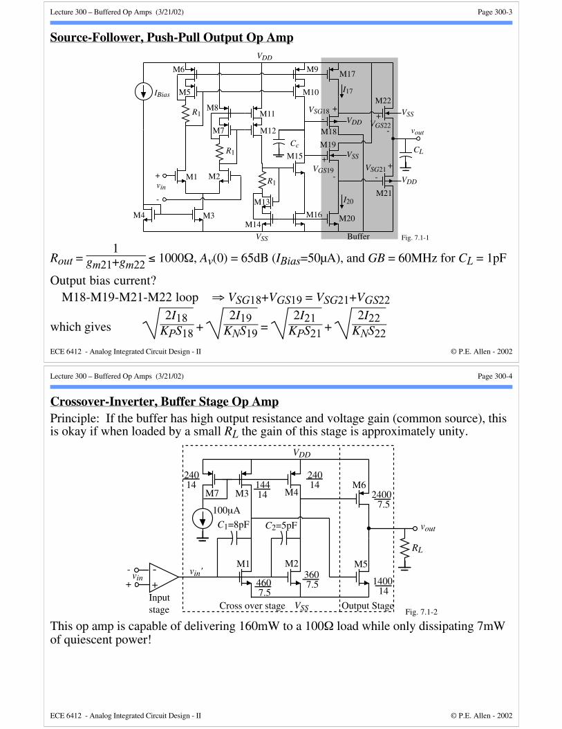
Source-Follower, Push-Pull Output Op Amp
vout
VDD
VDD
Cc
-
+vin
M1 M2
M3
VSS
R1
M5
M6
R1
M7
M8
R1
M13
M14
VSS
VDD
VSS
M22
M21
IBias
M9
M10
M11
M12
M4
M17
M18
M15
M16
M19
M20
Fig. 7.1-1
CL
Buffer
-+VSG18
-+VSG21
-
+VGS19
-
+VGS22
I17
I20
Rout = 1
gm21+gm22 ≤ 1000Ω, Av(0) = 65dB (IBias=50µA), and GB = 60MHz for CL = 1pF
Output bias current?M18-M19-M21-M22 loop ⇒ VSG18+VGS19 = VSG21+VGS22
which gives2I18
KPS18 + 2I19
KNS19 = 2I21
KPS21 + 2I22
KNS22
Lecture 300 – Buffered Op Amps (3/21/02) Page 300-4
ECE 6412 - Analog Integrated Circuit Design - II © P.E. Allen - 2002
Crossover-Inverter, Buffer Stage Op AmpPrinciple: If the buffer has high output resistance and voltage gain (common source), thisis okay if when loaded by a small RL the gain of this stage is approximately unity.
-
+vin
M1 M2
M3 M4
M5
M6M7
vout
VDD
VSS
C2=5pF
RL
+-
C1=8pF
100µA
140014
24007.5
24014144
14
24014
4607.5
3607.5
Cross over stage Output StageFig. 7.1-2
Inputstage
vin'
This op amp is capable of delivering 160mW to a 100Ω load while only dissipating 7mWof quiescent power!
Lecture 300 – Buffered Op Amps (3/21/02) Page 300-5
ECE 6412 - Analog Integrated Circuit Design - II © P.E. Allen - 2002
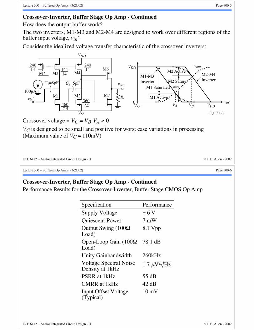
Crossover-Inverter, Buffer Stage Op Amp - ContinuedHow does the output buffer work?The two inverters, M1-M3 and M2-M4 are designed to work over different regions of thebuffer input voltage, vin’.
Consider the idealized voltage transfer characteristic of the crossover inverters:
VDDVA
M2 Active
M2 Satur-ated
M1 Active
M1 Saturated
VB
M1-M3Inverter
M2-M4Inverter
0 vin'
Fig. 7.1-3
M1 M2
M3 M4M7
vout
VDD
VSS
C2=5pFC1=8pF
100µA
24014144
14
24014
4607.5
3607.5
vin'
M6
M7 RL
voutVDD
VSS
Crossover voltage ≡ VC = VB-VA ≥ 0
VC is designed to be small and positive for worst case variations in processing(Maximum value of VC ≈ 110mV)
Lecture 300 – Buffered Op Amps (3/21/02) Page 300-6
ECE 6412 - Analog Integrated Circuit Design - II © P.E. Allen - 2002
Crossover-Inverter, Buffer Stage Op Amp - ContinuedPerformance Results for the Crossover-Inverter, Buffer Stage CMOS Op Amp
Specification PerformanceSupply Voltage ± 6 VQuiescent Power 7 mWOutput Swing (100ΩLoad)
8.1 Vpp
Open-Loop Gain (100ΩLoad)
78.1 dB
Unity Gainbandwidth 260kHzVoltage Spectral NoiseDensity at 1kHz
1.7 µV/ Hz
PSRR at 1kHz 55 dBCMRR at 1kHz 42 dBInput Offset Voltage(Typical)
10 mV
Lecture 300 – Buffered Op Amps (3/21/02) Page 300-7
ECE 6412 - Analog Integrated Circuit Design - II © P.E. Allen - 2002
Compensation of Op Amps with Output AmplifiersCompensation of a three-stage amplifier:This op amp introduces a third pole, p’3 (whatabout zeros?)With no compensation,
Vout(s)Vin(s) =
-Avo
s
p’1 - 1
s
p’2 - 1
s
p’3 - 1
Illustration of compensation choices:
p1'p2'p3' p1
p2
p3
jω
σp1'p2'p3' p1
p2
p3=
jω
σ
Miller compensation applied around both the second and the third stage.
Miller compensation applied around the second stage only. Fig. 7.1-5
Compensated polesUncompensated poles
vin vout+-
x1v2
Unbufferedop amp
Outputstage
Polesp1' and p2'
Pole p3'
+
-
Fig. 7.1-4
CL RL
Lecture 300 – Buffered Op Amps (3/21/02) Page 300-8
ECE 6412 - Analog Integrated Circuit Design - II © P.E. Allen - 2002
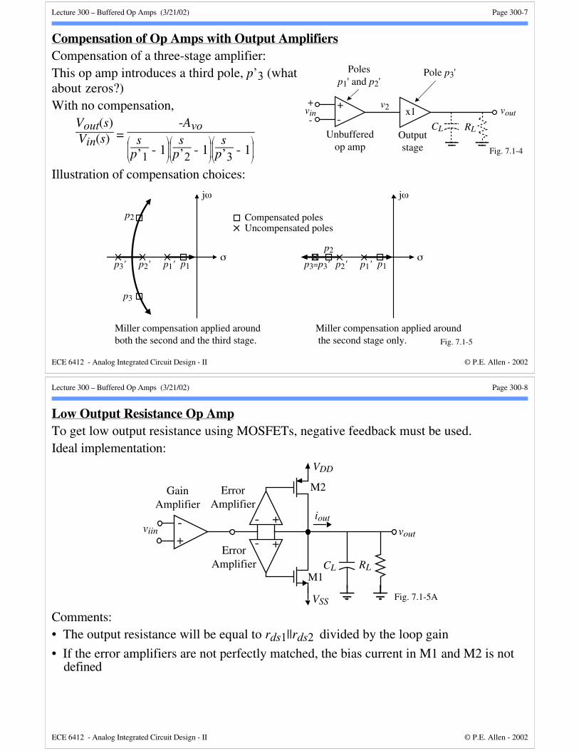
Low Output Resistance Op AmpTo get low output resistance using MOSFETs, negative feedback must be used.Ideal implementation:
CL RL
viin vout
iout
VDD
M2
M1
Fig. 7.1-5A
+-
+-
ErrorAmplifier
ErrorAmplifier
VSS
+-
GainAmplifier
Comments:• The output resistance will be equal to rds1||rds2 divided by the loop gain
• If the error amplifiers are not perfectly matched, the bias current in M1 and M2 is notdefined
Lecture 300 – Buffered Op Amps (3/21/02) Page 300-9
ECE 6412 - Analog Integrated Circuit Design - II © P.E. Allen - 2002
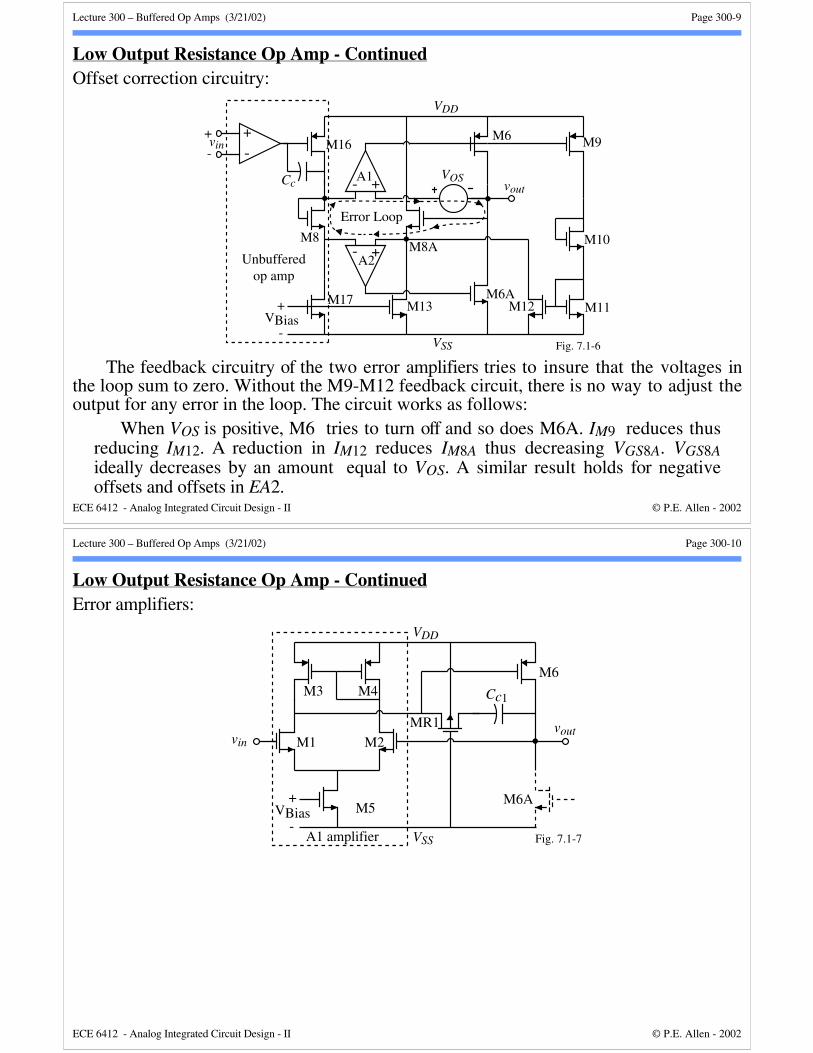
Low Output Resistance Op Amp - ContinuedOffset correction circuitry:
-
+vin
A1
M16 M9
vout
VDD
VSS
VBias+
-
Cc
+-
+-
+-M8
M17
M8A
M13M6A
M6
M12 M11
M10
A2
VOS
Error Loop
Fig. 7.1-6
Unbufferedop amp
The feedback circuitry of the two error amplifiers tries to insure that the voltages inthe loop sum to zero. Without the M9-M12 feedback circuit, there is no way to adjust theoutput for any error in the loop. The circuit works as follows:
When VOS is positive, M6 tries to turn off and so does M6A. IM9 reduces thusreducing IM12. A reduction in IM12 reduces IM8A thus decreasing VGS8A. VGS8Aideally decreases by an amount equal to VOS. A similar result holds for negativeoffsets and offsets in EA2.
Lecture 300 – Buffered Op Amps (3/21/02) Page 300-10
ECE 6412 - Analog Integrated Circuit Design - II © P.E. Allen - 2002
Low Output Resistance Op Amp - ContinuedError amplifiers:
vin M1 M2
M3 M4
M5
M6
M6A
vout
VDD
VSS
VBias+
-
Cc1
A1 amplifier
MR1
Fig. 7.1-7
Lecture 300 – Buffered Op Amps (3/21/02) Page 300-11
ECE 6412 - Analog Integrated Circuit Design - II © P.E. Allen - 2002
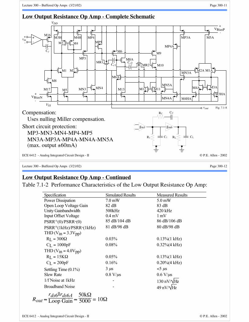
Low Output Resistance Op Amp - Complete Schematic
Compensation:Uses nulling Miller compensation.
Short circuit protection:MP3-MN3-MN4-MP4-MP5MN3A-MP3A-MP4A-MN4A-MN5A(max. output ±60mA)
M2
M3 M4
M5
M1
vout
VDD
VSS
VBiasN+
-
Cc
+-
VBiasP+
-
Cc1
M16M3H M4H MP4
MP3
MP5
MR1
M8
M17 MN3 MN4
M6
M6A
M13 M12 M11
MR2Cc2
M8A
M9
MN5A
MN4A
MN3A
MP4A
MP3A
M4HA
M4A M3A
M3HA
M1AM2A
M5Avin+
-
Fig. 7.1-8
M10
RC
R1 RL CL
CC
C1
gm1 gm6
Lecture 300 – Buffered Op Amps (3/21/02) Page 300-12
ECE 6412 - Analog Integrated Circuit Design - II © P.E. Allen - 2002
Low Output Resistance Op Amp - ContinuedTable 7.1-2 Performance Characteristics of the Low Output Resistance Op Amp:
Specification Simulated Results Measured ResultsPower Dissipation 7.0 mW 5.0 mWOpen Loop Voltage Gain 82 dB 83 dBUnity Gainbandwidth 500kHz 420 kHzInput Offset Voltage 0.4 mV 1 mVPSRR+(0)/PSRR-(0) 85 dB/104 dB 86 dB/106 dB
PSRR+(1kHz)/PSRR-(1kHz) 81 dB/98 dB 80 dB/98 dBTHD (Vin = 3.3Vpp) RL = 300Ω 0.03% 0.13%(1 kHz) CL = 1000pF 0.08% 0.32%(4 kHz)THD (Vin = 4.0Vpp) RL = 15KΩ 0.05% 0.13%(1 kHz) CL = 200pF 0.16% 0.20%(4 kHz)
Settling Time (0.1%) 3 µs <5 µsSlew Rate 0.8 V/µs 0.6 V/µs1/f Noise at 1kHz - 130 nV/ HzBroadband Noise - 49 nV/ Hz
Rout ≈ rds6||rds6ALoop Gain ≈
50kΩ5000 = 10Ω
Lecture 300 – Buffered Op Amps (3/21/02) Page 300-13
ECE 6412 - Analog Integrated Circuit Design - II © P.E. Allen - 2002
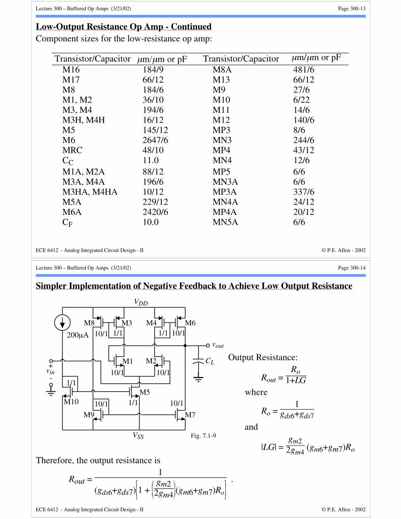
Low-Output Resistance Op Amp - ContinuedComponent sizes for the low-resistance op amp:
Transistor/Capacitor µm/µm or pF Transistor/Capacitor µm/µm or pFM16 184/9 M8A 481/6M17 66/12 M13 66/12M8 184/6 M9 27/6M1, M2 36/10 M10 6/22M3, M4 194/6 M11 14/6M3H, M4H 16/12 M12 140/6M5 145/12 MP3 8/6M6 2647/6 MN3 244/6MRC 48/10 MP4 43/12CC 11.0 MN4 12/6M1A, M2A 88/12 MP5 6/6M3A, M4A 196/6 MN3A 6/6M3HA, M4HA 10/12 MP3A 337/6M5A 229/12 MN4A 24/12M6A 2420/6 MP4A 20/12CF 10.0 MN5A 6/6
Lecture 300 – Buffered Op Amps (3/21/02) Page 300-14
ECE 6412 - Analog Integrated Circuit Design - II © P.E. Allen - 2002
Simpler Implementation of Negative Feedback to Achieve Low Output Resistance
Output Resistance:
Rout = Ro
1+LG
where
Ro = 1
gds6+gds7
and
|LG| = gm22gm4
(gm6+gm7)Ro
Therefore, the output resistance is
Rout = 1
(gds6+gds7)
1 +
gm2
2gm4 (gm6+gm7)Ro
.
-
+vin
M1 M2
M3 M4
M5
M6
M7
vout
VDD
VSS
CL
M8
M10
M9
Fig. 7.1-9
1/1 10/1200µA 10/1
10/1 10/1
1/1
1/1
1/1
10/1 10/1
Lecture 300 – Buffered Op Amps (3/21/02) Page 300-15
ECE 6412 - Analog Integrated Circuit Design - II © P.E. Allen - 2002
Example 7.1-1 - Low Output Resistance Using the Simple Shunt Negative FeedbackBufferFind the output resistance of above op amp using the model parameters of Table 3.1-2.SolutionThe current flowing in the output transistors, M6 and M7, is 1mA which gives Ro of
Ro = 1
(λN+λP)1mA = 10000.09 = 11.11kΩ
To calculate the loop gain, we find that
gm2 = 2KN’·10·100µA = 469µS
gm4 = 2KP’·1·100µA = 100µS
and gm6 = 2KP’·10·1000µA = 1mS
Therefore, the loop gain is
|LG| = 469100 12·11.11 = 104.2
Solving for the output resistance, Rout, gives
Rout = 11.11kΩ1 + 104.2 = 106Ω (Assumes that RL is large)
Lecture 300 – Buffered Op Amps (3/21/02) Page 300-16
ECE 6412 - Analog Integrated Circuit Design - II © P.E. Allen - 2002
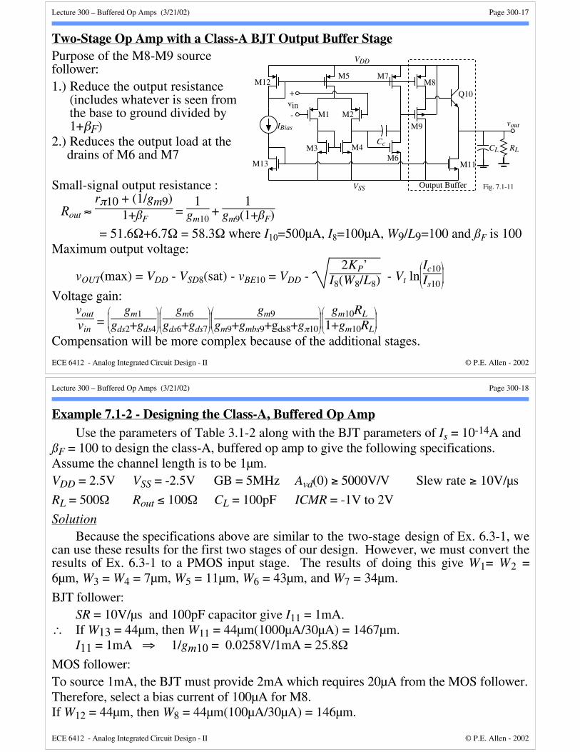
BJTs Available in CMOS TechnologyIllustration of an NPN substrate BJT available in a p-well CMOS technology:
n- substrate (Collector)
p- well (Base)
n+ (Emitter) p+
n+
Emitter Base Collector(VDD)
Collector (VDD)
Emitter
Base
Fig. 7.1-10
Comments:• gm of the BJT is larger than the FET so that the output resistance w/o feedback is lower
• Can use the lateral or substrate BJT but since the collector is on ac ground, thesubstrate BJT is preferred
• Current is required to drive the BJT
Lecture 300 – Buffered Op Amps (3/21/02) Page 300-17
ECE 6412 - Analog Integrated Circuit Design - II © P.E. Allen - 2002
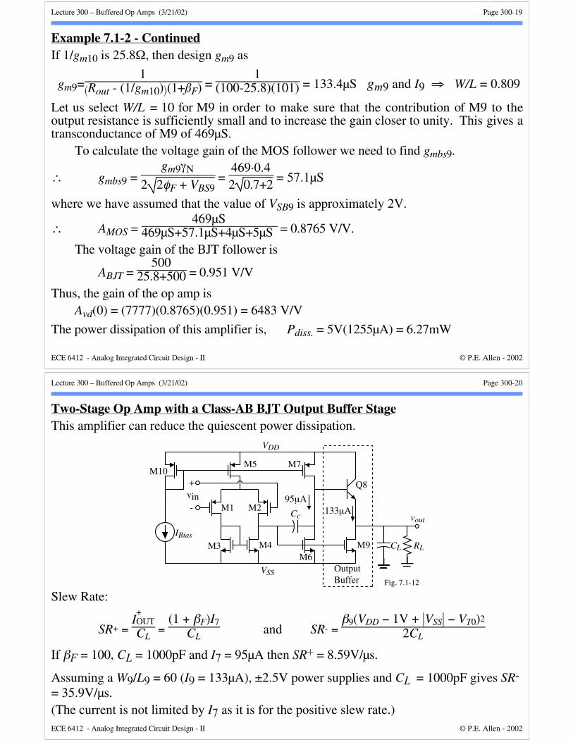
Two-Stage Op Amp with a Class-A BJT Output Buffer StagePurpose of the M8-M9 sourcefollower:1.) Reduce the output resistance
(includes whatever is seen fromthe base to ground divided by1+βF)
2.) Reduces the output load at thedrains of M6 and M7
Small-signal output resistance :
Rout ≈ rπ10 + (1/gm9)
1+ßF =
1gm10
+ 1
gm9(1+ßF)
= 51.6Ω+6.7Ω = 58.3Ω where I10=500µA, I8=100µA, W9/L9=100 and ßF is 100Maximum output voltage:
vOUT(max) = VDD - VSD8(sat) - vBE10 = VDD - 2KP’
I8(W8/L8) - Vt ln
Ic10
Is10
Voltage gain:voutvin
=
gm1
gds2+gds4
gm6
gds6+gds7
gm9
gm9+gmbs9+gds8+gπ10
gm10RL
1+gm10RL
Compensation will be more complex because of the additional stages.
M1 M2
M3 M4
M5
M6
M7
vout
VDD
VSS
CcCL
IBias
Q10
M11
M12
M13
Fig. 7.1-11
M8
M9
Output Buffer
RL
vin
+
-
Lecture 300 – Buffered Op Amps (3/21/02) Page 300-18
ECE 6412 - Analog Integrated Circuit Design - II © P.E. Allen - 2002
Example 7.1-2 - Designing the Class-A, Buffered Op AmpUse the parameters of Table 3.1-2 along with the BJT parameters of Is = 10-14A and
ßF = 100 to design the class-A, buffered op amp to give the following specifications.Assume the channel length is to be 1µm.VDD = 2.5V VSS = -2.5V GB = 5MHz Avd(0) ≥ 5000V/V Slew rate ≥ 10V/µs
RL = 500Ω Rout ≤ 100Ω CL = 100pF ICMR = -1V to 2V
SolutionBecause the specifications above are similar to the two-stage design of Ex. 6.3-1, we
can use these results for the first two stages of our design. However, we must convert theresults of Ex. 6.3-1 to a PMOS input stage. The results of doing this give W1= W2 =6µm, W3 = W4 = 7µm, W5 = 11µm, W6 = 43µm, and W7 = 34µm.
BJT follower:SR = 10V/µs and 100pF capacitor give I11 = 1mA.
∴ If W13 = 44µm, then W11 = 44µm(1000µA/30µA) = 1467µm.I11 = 1mA ⇒ 1/gm10 = 0.0258V/1mA = 25.8Ω
MOS follower:To source 1mA, the BJT must provide 2mA which requires 20µA from the MOS follower. Therefore, select a bias current of 100µA for M8. If W12 = 44µm, then W8 = 44µm(100µA/30µA) = 146µm.
Lecture 300 – Buffered Op Amps (3/21/02) Page 300-19
ECE 6412 - Analog Integrated Circuit Design - II © P.E. Allen - 2002
Example 7.1-2 - ContinuedIf 1/gm10 is 25.8Ω, then design gm9 as
gm9=1
Rout - (1/gm10) (1+ßF) = 1
(100-25.8)(101) = 133.4µS gm9 and I9 ⇒ W/L = 0.809
Let us select W/L = 10 for M9 in order to make sure that the contribution of M9 to theoutput resistance is sufficiently small and to increase the gain closer to unity. This gives atransconductance of M9 of 469µS.
To calculate the voltage gain of the MOS follower we need to find gmbs9.
∴ gmbs9 = gm9γN
2 2φF + VBS9 =
469·0.42 0.7+2 = 57.1µS
where we have assumed that the value of VSB9 is approximately 2V.
∴ AMOS = 469µS
469µS+57.1µS+4µS+5µS = 0.8765 V/V.
The voltage gain of the BJT follower is
ABJT = 500
25.8+500 = 0.951 V/V
Thus, the gain of the op amp isAvd(0) = (7777)(0.8765)(0.951) = 6483 V/V
The power dissipation of this amplifier is, Pdiss. = 5V(1255µA) = 6.27mW
Lecture 300 – Buffered Op Amps (3/21/02) Page 300-20
ECE 6412 - Analog Integrated Circuit Design - II © P.E. Allen - 2002
Two-Stage Op Amp with a Class-AB BJT Output Buffer StageThis amplifier can reduce the quiescent power dissipation.
M1 M2
M3 M4
M5
M6
M7
vout
VDD
VSS
Cc
CL
vin
IBias
Q8
M10
Fig. 7.1-12
M9
Output Buffer
RL
+
-95µA
133µA
Slew Rate:
SR+ = I+OUT
CL =
(1 + βF)I7CL
and SR- = β9(VDD − 1V + |VSS| − VT0)2
2CL
If βF = 100, CL = 1000pF and I7 = 95µA then SR+ = 8.59V/µs.
Assuming a W9/L9 = 60 (I9 = 133µA), ±2.5V power supplies and CL = 1000pF gives SR-
= 35.9V/µs.(The current is not limited by I7 as it is for the positive slew rate.)
Lecture 300 – Buffered Op Amps (3/21/02) Page 300-21
ECE 6412 - Analog Integrated Circuit Design - II © P.E. Allen - 2002
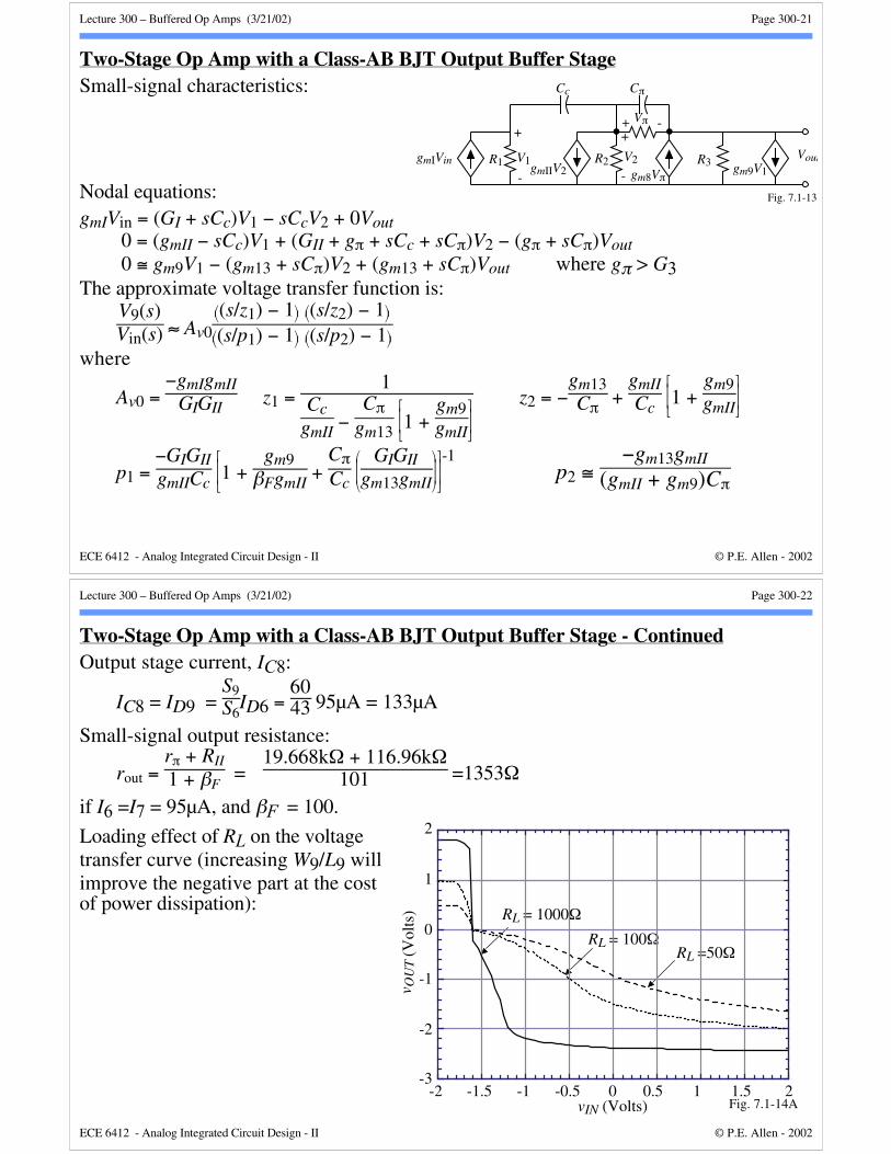
Two-Stage Op Amp with a Class-AB BJT Output Buffer StageSmall-signal characteristics:
Nodal equations:gmIVin = (GI + sCc)V1 − sCcV2 + 0Vout
0 = (gmII − sCc)V1 + (GII + gπ + sCc + sCπ)V2 − (gπ + sCπ)Vout 0 ≅ gm9V1 − (gm13 + sCπ)V2 + (gm13 + sCπ)Vout where gπ > G3
The approximate voltage transfer function is:V9(s)Vin(s) ≈ Av0
(s/z1) − 1 (s/z2) − 1
(s/p1) − 1 (s/p2) − 1where
Av0 = −gmIgmII
GIGIIz1 =
1Cc
gmII −
Cπgm13
1 + gm9gmII
z2 = −gm13Cπ +
gmIICc
1 + gm9gmII
p1 = −GIGIIgmIICc
1 + gm9
βFgmII +
CπCc
GIGII
gm13gmII
-1p2 ≅
−gm13gmII
(gmII + gm9)Cπ
VoutgmIVin R1
+
V1
-gmIIV2
R2
Cc
+
V2
-
Cπ
+ -Vπ
gm8Vπ
R3 gm9V1
Fig. 7.1-13
Lecture 300 – Buffered Op Amps (3/21/02) Page 300-22
ECE 6412 - Analog Integrated Circuit Design - II © P.E. Allen - 2002
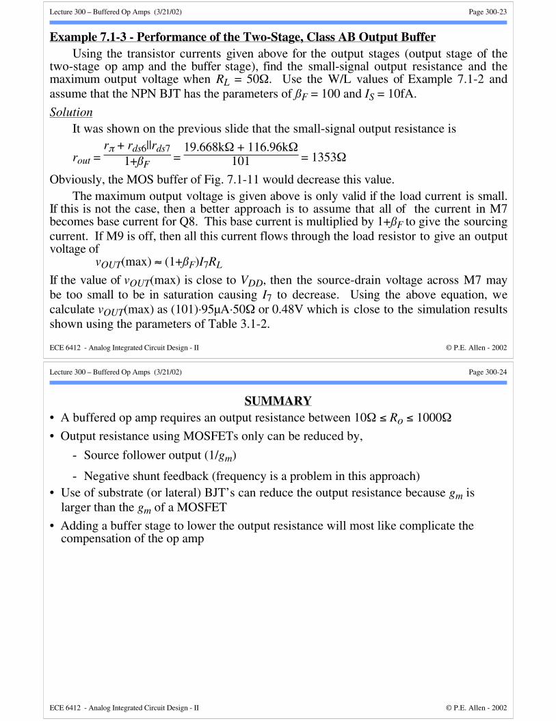
Two-Stage Op Amp with a Class-AB BJT Output Buffer Stage - ContinuedOutput stage current, IC8:
IC8 = ID9 = S9S6
ID6 = 6043 95µA = 133µA
Small-signal output resistance:
rout = rπ + RII
1 + βF =
19.668kΩ + 116.96kΩ101 =1353Ω
if I6 =I7 = 95µA, and βF = 100.
Loading effect of RL on the voltagetransfer curve (increasing W9/L9 willimprove the negative part at the costof power dissipation):
-3
-2
-1
0
1
2
-2 -1.5 -1 -0.5 0
v OU
T (V
olts
)
vIN (Volts)
RL =50ΩRL = 100Ω
RL = 1000Ω
Fig. 7.1-14A0.5 1 1.5 2
Lecture 300 – Buffered Op Amps (3/21/02) Page 300-23
ECE 6412 - Analog Integrated Circuit Design - II © P.E. Allen - 2002
Example 7.1-3 - Performance of the Two-Stage, Class AB Output BufferUsing the transistor currents given above for the output stages (output stage of the
two-stage op amp and the buffer stage), find the small-signal output resistance and themaximum output voltage when RL = 50Ω. Use the W/L values of Example 7.1-2 andassume that the NPN BJT has the parameters of ßF = 100 and IS = 10fA.
SolutionIt was shown on the previous slide that the small-signal output resistance is
rout = rπ + rds6||rds7
1+ßF =
19.668kΩ + 116.96kΩ101 = 1353Ω
Obviously, the MOS buffer of Fig. 7.1-11 would decrease this value.The maximum output voltage is given above is only valid if the load current is small.
If this is not the case, then a better approach is to assume that all of the current in M7becomes base current for Q8. This base current is multiplied by 1+ßF to give the sourcingcurrent. If M9 is off, then all this current flows through the load resistor to give an outputvoltage of
vOUT(max) ≈ (1+ßF)I7RL
If the value of vOUT(max) is close to VDD, then the source-drain voltage across M7 maybe too small to be in saturation causing I7 to decrease. Using the above equation, wecalculate vOUT(max) as (101)·95µA·50Ω or 0.48V which is close to the simulation resultsshown using the parameters of Table 3.1-2.
Lecture 300 – Buffered Op Amps (3/21/02) Page 300-24
ECE 6412 - Analog Integrated Circuit Design - II © P.E. Allen - 2002
SUMMARY• A buffered op amp requires an output resistance between 10Ω ≤ Ro ≤ 1000Ω
• Output resistance using MOSFETs only can be reduced by,
- Source follower output (1/gm)
- Negative shunt feedback (frequency is a problem in this approach)• Use of substrate (or lateral) BJT’s can reduce the output resistance because gm is
larger than the gm of a MOSFET
• Adding a buffer stage to lower the output resistance will most like complicate thecompensation of the op amp

![DOCUMENT RESUME ED 368 352 AUTHOR Brown, G:rald R. TITLE ... · Marketing is discovering the needs of the clients and meeting them (the needs I mean). [Define, OSLA]. Before sophisticated](https://img.pdfslide.us/doc/110x75/60369753a55fc81705104b35/document-resume-ed-368-352-author-brown-grald-r-title-marketing-is-discovering.jpg)


![ajguwriwiswcui^^- ::::::::::ii{^ 198… · IJptpn George W 368-2i(u Walker Dennis N 36S-2]Q9 Watson Gordon BoxS2 .... . , 368-2473 Watson,dohnR i'., '368-22u Watts Clark 368-2469](https://img.pdfslide.us/doc/110x75/5f48a2995403983c750e8274/ajguwriwiswcui-ii-198-ijptpn-george-w-368-2iu-walker-dennis-n.jpg)