Embed Size (px)
Citation preview
PrefaceSLDU010A–March 2012–Revised August 2014
Read This First
About This ManualThis user’s guide describes the characteristics, operation, and use of the PGA400-Q1EVM. An EVMoverview, graphical user-interface (GUI) description, interface requirements, and complete schematic areincluded in this document.
How to Use This ManualThis document contains the following chapters:1. Chapter 1: Power Supply Requirements and Connections2. Chapter 2: Jumper Settings3. Chapter 3: Sensor Inputs and Simulators4. Chapter 4: PGA400-Q1 VOUT1 and VOUT2 Output Circuitry5. Chapter 5: PGA400-Q1 Communication interfaces6. Chapter 6: Controlling the PGA400-Q1 Memory Spaces with the GUI7. Chapter 7: Controlling the PGA400-Q1 Functions with the GUI8. Chapter 8: PGA400-Q1 EVM Schematics and Layout Drawings
EVM Overview
FeaturesThe EVM includes the following features:• Single 12-VDC power-supply input for basic operation• Resistive and capacitive sensor simulators• PC Control with a GUI and USB communications board• One-wire-interface (OWI) activation and communication circuitry• RS-232 transceiver for UART testing and debug
IntroductionThe PGA400-Q1 device is a generic-sensor interface integrated circuit (IC) for resistive and capacitivesensors. The device features a configurable analog front-end (AFE) with diagnostics, sigma-delta ADC,8051 microcontroller, DACs, SPI, I2C, and a one-wire interface (OWI).
1SLDU010A–March 2012–Revised August 2014 Read This FirstSubmit Documentation Feedback
Copyright © 2012–2014, Texas Instruments Incorporated
Chapter 1SLDU010A–March 2012–Revised August 2014
Power Supply Requirements and Connections
The PGA400-Q1EVM has only one main 9-VDC to 12-VDC power connector that supplies power to theentire board. The user is required to connect a power supply to the banana jacks, P1 VPWR and P3 GNDor use the screw terminal P2. Figure 1-1 shows an example using the banana jack connections.
Figure 1-1. Minimum Power Connections to the PGA400-Q1 EVM
Configure the power supply based on the following table:
CONNECTION VOLTAGE CURRENT LIMITVPWR 9 – 12 VDC 100 mA
When powered, the D30 LED should light up and the EVM should draw between 30 and 55 mA dependingon what state of operation the device is in.
2 Power Supply Requirements and Connections SLDU010A–March 2012–Revised August 2014Submit Documentation Feedback
Copyright © 2012–2014, Texas Instruments Incorporated
www.ti.com Controlling and Powering the R2D2 EVM through TI-GER USB Board
1.1 Controlling and Powering the R2D2 EVM through TI-GER USB BoardThe PGA400-Q1 EVM is shipped with a TI-GER USB communication board that provides a link from thePC controlled GUI (see Chapter 6) to the EVM. The user must connect the TI-GER board to the PGA400-Q1 by connecting the 15 × 2 100-mil female header on the TI-GER board to P6, the male 15 × 2 headeron the PGA400-Q1 EVM. The TI logo on the TI-GER board should face up when it is plugged in. Figure 1-2 shows the TI-GER board connected to the PGA400-Q1 EVM.
Figure 1-2. Connecting the TI-GER USB Communication Board to the PGA400-Q1 EVM
1.2 Power Supply LEDsLEDs are installed in several places on the EVM to provide the user an indication that power-supplies areconnected correctly. The VDD and VP_OTP connections on the PGA400-Q1 device have LEDs to indicatethat power is applied. Also, two LEDS indicate that the USB power supplies on the TI-GER boards arepresent.
Table 1-1. Power Supply LED Connections
LED SUPPLYD2 TI-GER 3.3 VD3 TI-GER 5 VD30 PGA400-Q1 VDD
D31 PGA400-Q1 VP_OTP
3SLDU010A–March 2012–Revised August 2014 Power Supply Requirements and ConnectionsSubmit Documentation Feedback
Copyright © 2012–2014, Texas Instruments Incorporated
Chapter 2SLDU010A–March 2012–Revised August 2014
Jumper Settings
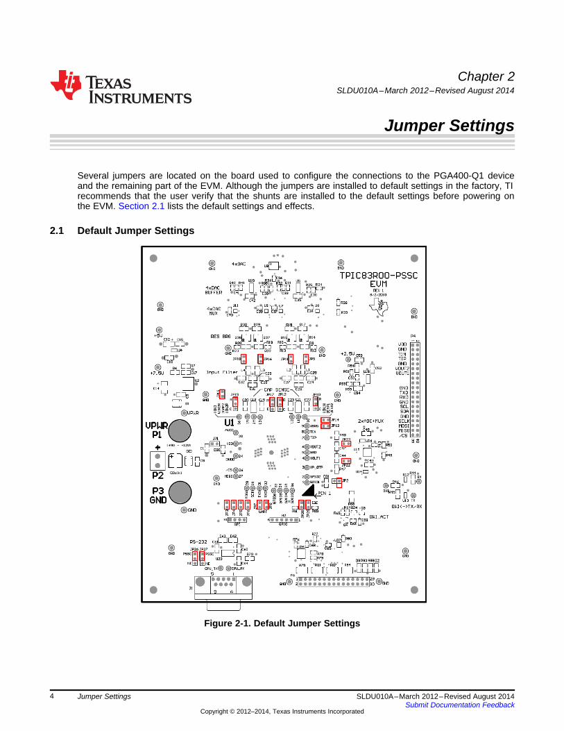
Several jumpers are located on the board used to configure the connections to the PGA400-Q1 deviceand the remaining part of the EVM. Although the jumpers are installed to default settings in the factory, TIrecommends that the user verify that the shunts are installed to the default settings before powering onthe EVM. Section 2.1 lists the default settings and effects.
2.1 Default Jumper Settings
Figure 2-1. Default Jumper Settings
4 Jumper Settings SLDU010A–March 2012–Revised August 2014Submit Documentation Feedback
Copyright © 2012–2014, Texas Instruments Incorporated
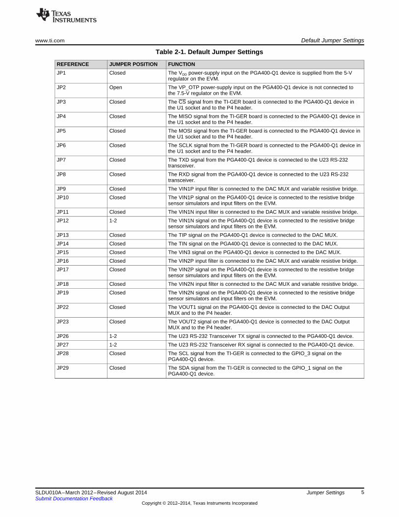
www.ti.com Default Jumper Settings
Table 2-1. Default Jumper Settings
REFERENCE JUMPER POSITION FUNCTIONJP1 Closed The VDD power-supply input on the PGA400-Q1 device is supplied from the 5-V
regulator on the EVM.JP2 Open The VP_OTP power-supply input on the PGA400-Q1 device is not connected to
the 7.5-V regulator on the EVM.JP3 Closed The CS signal from the TI-GER board is connected to the PGA400-Q1 device in
the U1 socket and to the P4 header.JP4 Closed The MISO signal from the TI-GER board is connected to the PGA400-Q1 device in
the U1 socket and to the P4 header.JP5 Closed The MOSI signal from the TI-GER board is connected to the PGA400-Q1 device in
the U1 socket and to the P4 header.JP6 Closed The SCLK signal from the TI-GER board is connected to the PGA400-Q1 device in
the U1 socket and to the P4 header.JP7 Closed The TXD signal from the PGA400-Q1 device is connected to the U23 RS-232
transceiver.JP8 Closed The RXD signal from the PGA400-Q1 device is connected to the U23 RS-232
transceiver.JP9 Closed The VIN1P input filter is connected to the DAC MUX and variable resistive bridge.JP10 Closed The VIN1P signal on the PGA400-Q1 device is connected to the resistive bridge
sensor simulators and input filters on the EVM.JP11 Closed The VIN1N input filter is connected to the DAC MUX and variable resistive bridge.JP12 1-2 The VIN1N signal on the PGA400-Q1 device is connected to the resistive bridge
sensor simulators and input filters on the EVM.JP13 Closed The TIP signal on the PGA400-Q1 device is connected to the DAC MUX.JP14 Closed The TIN signal on the PGA400-Q1 device is connected to the DAC MUX.JP15 Closed The VIN3 signal on the PGA400-Q1 device is connected to the DAC MUX.JP16 Closed The VIN2P input filter is connected to the DAC MUX and variable resistive bridge.JP17 Closed The VIN2P signal on the PGA400-Q1 device is connected to the resistive bridge
sensor simulators and input filters on the EVM.JP18 Closed The VIN2N input filter is connected to the DAC MUX and variable resistive bridge.JP19 Closed The VIN2N signal on the PGA400-Q1 device is connected to the resistive bridge
sensor simulators and input filters on the EVM.JP22 Closed The VOUT1 signal on the PGA400-Q1 device is connected to the DAC Output
MUX and to the P4 header.JP23 Closed The VOUT2 signal on the PGA400-Q1 device is connected to the DAC Output
MUX and to the P4 header.JP26 1-2 The U23 RS-232 Transceiver TX signal is connected to the PGA400-Q1 device.JP27 1-2 The U23 RS-232 Transceiver RX signal is connected to the PGA400-Q1 device.JP28 Closed The SCL signal from the TI-GER is connected to the GPIO_3 signal on the
PGA400-Q1 device.JP29 Closed The SDA signal from the TI-GER is connected to the GPIO_1 signal on the
PGA400-Q1 device.
5SLDU010A–March 2012–Revised August 2014 Jumper SettingsSubmit Documentation Feedback
Copyright © 2012–2014, Texas Instruments Incorporated
R C
R C
R C
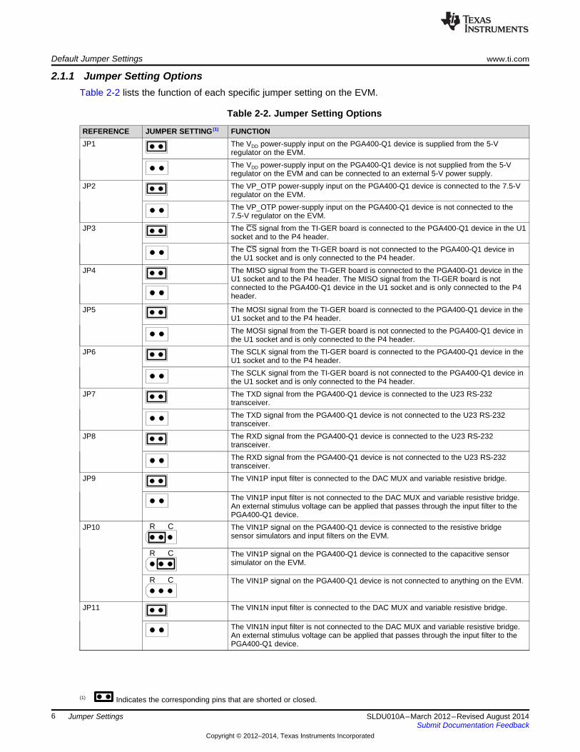
(1) Indicates the corresponding pins that are shorted or closed.
Default Jumper Settings www.ti.com
2.1.1 Jumper Setting OptionsTable 2-2 lists the function of each specific jumper setting on the EVM.
Table 2-2. Jumper Setting Options
REFERENCE JUMPER SETTING (1) FUNCTIONJP1 The VDD power-supply input on the PGA400-Q1 device is supplied from the 5-V
regulator on the EVM.The VDD power-supply input on the PGA400-Q1 device is not supplied from the 5-Vregulator on the EVM and can be connected to an external 5-V power supply.
JP2 The VP_OTP power-supply input on the PGA400-Q1 device is connected to the 7.5-Vregulator on the EVM.The VP_OTP power-supply input on the PGA400-Q1 device is not connected to the7.5-V regulator on the EVM.
JP3 The CS signal from the TI-GER board is connected to the PGA400-Q1 device in the U1socket and to the P4 header.The CS signal from the TI-GER board is not connected to the PGA400-Q1 device inthe U1 socket and is only connected to the P4 header.
JP4 The MISO signal from the TI-GER board is connected to the PGA400-Q1 device in theU1 socket and to the P4 header. The MISO signal from the TI-GER board is notconnected to the PGA400-Q1 device in the U1 socket and is only connected to the P4header.
JP5 The MOSI signal from the TI-GER board is connected to the PGA400-Q1 device in theU1 socket and to the P4 header.The MOSI signal from the TI-GER board is not connected to the PGA400-Q1 device inthe U1 socket and is only connected to the P4 header.
JP6 The SCLK signal from the TI-GER board is connected to the PGA400-Q1 device in theU1 socket and to the P4 header.The SCLK signal from the TI-GER board is not connected to the PGA400-Q1 device inthe U1 socket and is only connected to the P4 header.
JP7 The TXD signal from the PGA400-Q1 device is connected to the U23 RS-232transceiver.The TXD signal from the PGA400-Q1 device is not connected to the U23 RS-232transceiver.
JP8 The RXD signal from the PGA400-Q1 device is connected to the U23 RS-232transceiver.The RXD signal from the PGA400-Q1 device is not connected to the U23 RS-232transceiver.
JP9 The VIN1P input filter is connected to the DAC MUX and variable resistive bridge.
The VIN1P input filter is not connected to the DAC MUX and variable resistive bridge.An external stimulus voltage can be applied that passes through the input filter to thePGA400-Q1 device.
JP10 The VIN1P signal on the PGA400-Q1 device is connected to the resistive bridgesensor simulators and input filters on the EVM.
The VIN1P signal on the PGA400-Q1 device is connected to the capacitive sensorsimulator on the EVM.
The VIN1P signal on the PGA400-Q1 device is not connected to anything on the EVM.
JP11 The VIN1N input filter is connected to the DAC MUX and variable resistive bridge.
The VIN1N input filter is not connected to the DAC MUX and variable resistive bridge.An external stimulus voltage can be applied that passes through the input filter to thePGA400-Q1 device.
6 Jumper Settings SLDU010A–March 2012–Revised August 2014Submit Documentation Feedback
Copyright © 2012–2014, Texas Instruments Incorporated
R C
R C
R C
R C
R C
R C
R C
R C
R C
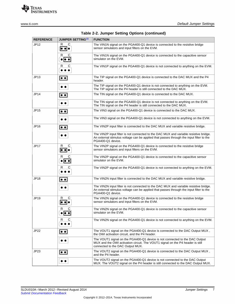
www.ti.com Default Jumper Settings
Table 2-2. Jumper Setting Options (continued)REFERENCE JUMPER SETTING (1) FUNCTIONJP12 The VIN1N signal on the PGA400-Q1 device is connected to the resistive bridge
sensor simulators and input filters on the EVM.
The VIN1N signal on the PGA400-Q1 device is connected to the capacitive sensorsimulator on the EVM.
The VIN1P signal on the PGA400-Q1 device is not connected to anything on the EVM.
JP13 The TIP signal on the PGA400-Q1 device is connected to the DAC MUX and the P4header.The TIP signal on the PGA400-Q1 device is not connected to anything on the EVM.The TIP signal on the P4 header is still connected to the DAC MUX.
JP14 The TIN signal on the PGA400-Q1 device is connected to the DAC MUX.
The TIN signal on the PGA400-Q1 device is not connected to anything on the EVM.The TIN signal on the P4 header is still connected to the DAC MUX.
JP15 The VIN3 signal on the PGA400-Q1 device is connected to the DAC MUX.
The VIN3 signal on the PGA400-Q1 device is not connected to anything on the EVM.
JP16 The VIN2P input filter is connected to the DAC MUX and variable resistive bridge.
The VIN2P input filter is not connected to the DAC MUX and variable resistive bridge.An external stimulus voltage can be applied that passes through the input filter to thePGA400-Q1 device.
JP17 The VIN2P signal on the PGA400-Q1 device is connected to the resistive bridgesensor simulators and input filters on the EVM.
The VIN2P signal on the PGA400-Q1 device is connected to the capacitive sensorsimulator on the EVM.
The VIN2P signal on the PGA400-Q1 device is not connected to anything on the EVM.
JP18 The VIN2N input filter is connected to the DAC MUX and variable resistive bridge.
The VIN2N input filter is not connected to the DAC MUX and variable resistive bridge.An external stimulus voltage can be applied that passes through the input filter to thePGA400-Q1 device.
JP19 The VIN2N signal on the PGA400-Q1 device is connected to the resistive bridgesensor simulators and input filters on the EVM.
The VIN2N signal on the PGA400-Q1 device is connected to the capacitive sensorsimulator on the EVM.
The VIN2N signal on the PGA400-Q1 device is not connected to anything on the EVM.
JP22 The VOUT1 signal on the PGA400-Q1 device is connected to the DAC Output MUX ,the OWI activation circuit, and the P4 header.The VOUT1 signal on the PGA400-Q1 device is not connected to the DAC OutputMUX and the OWI activation circuit. The VOUT1 signal on the P4 header is stillconnected to the DAC Output MUX.
JP23 The VOUT2 signal on the PGA400-Q1 device is connected to the DAC Output MUX ,and the P4 header.The VOUT2 signal on the PGA400-Q1 device is not connected to the DAC OutputMUX. The VOUT2 signal on the P4 header is still connected to the DAC Output MUX.
7SLDU010A–March 2012–Revised August 2014 Jumper SettingsSubmit Documentation Feedback
Copyright © 2012–2014, Texas Instruments Incorporated
1 3
1 3
1 3
1 3
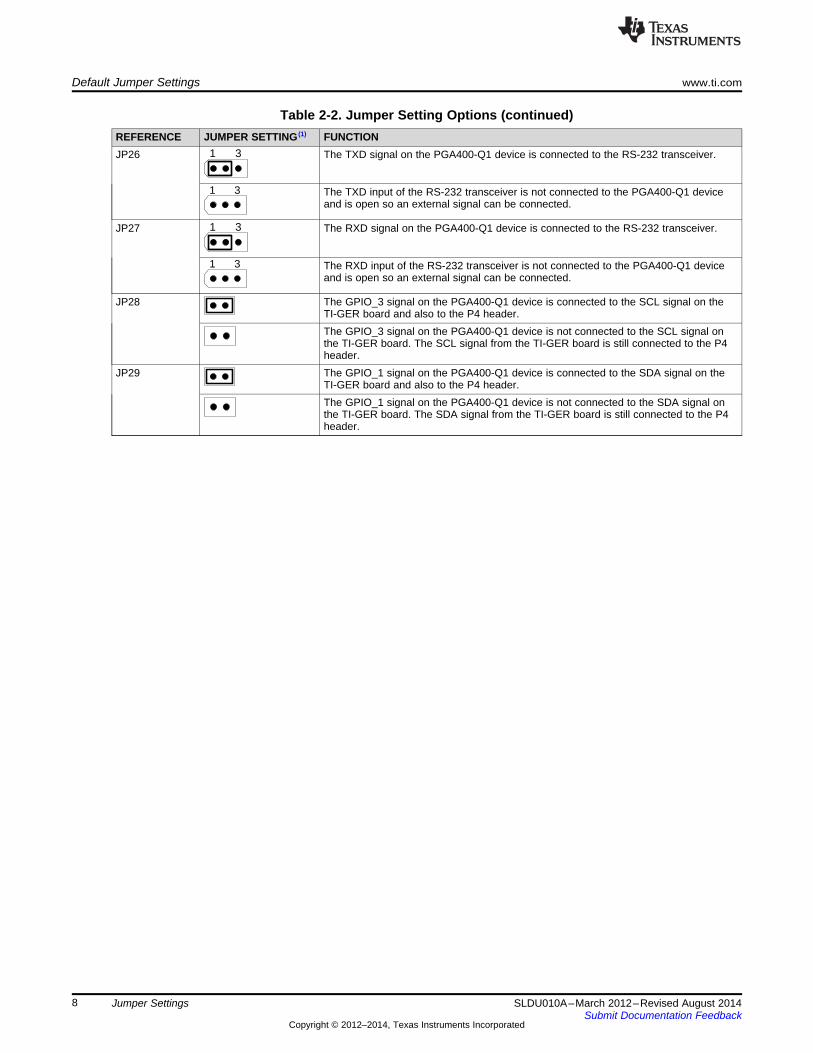
Default Jumper Settings www.ti.com
Table 2-2. Jumper Setting Options (continued)REFERENCE JUMPER SETTING (1) FUNCTIONJP26 The TXD signal on the PGA400-Q1 device is connected to the RS-232 transceiver.
The TXD input of the RS-232 transceiver is not connected to the PGA400-Q1 deviceand is open so an external signal can be connected.
JP27 The RXD signal on the PGA400-Q1 device is connected to the RS-232 transceiver.
The RXD input of the RS-232 transceiver is not connected to the PGA400-Q1 deviceand is open so an external signal can be connected.
JP28 The GPIO_3 signal on the PGA400-Q1 device is connected to the SCL signal on theTI-GER board and also to the P4 header.The GPIO_3 signal on the PGA400-Q1 device is not connected to the SCL signal onthe TI-GER board. The SCL signal from the TI-GER board is still connected to the P4header.
JP29 The GPIO_1 signal on the PGA400-Q1 device is connected to the SDA signal on theTI-GER board and also to the P4 header.The GPIO_1 signal on the PGA400-Q1 device is not connected to the SDA signal onthe TI-GER board. The SDA signal from the TI-GER board is still connected to the P4header.
8 Jumper Settings SLDU010A–March 2012–Revised August 2014Submit Documentation Feedback
Copyright © 2012–2014, Texas Instruments Incorporated
DAC1 x2
ADC3
DAC2
DAC3
ADC4
DAC4
x2
x2
x2
VBRG
VBRG
NCTIP
NCTIN
NCVIN3
NCNC
NC = No Connect
Red Text = Electrical Net
VIN2P
VIN2N
ICAP2
MUX
MUX
MUX
MUX
MUX
MUX
VIN1P
VIN1N
ICAP1
Input Filter
Input Filter
Input Filter
Input Filter
Chapter 3SLDU010A–March 2012–Revised August 2014
Sensor Inputs and Simulators
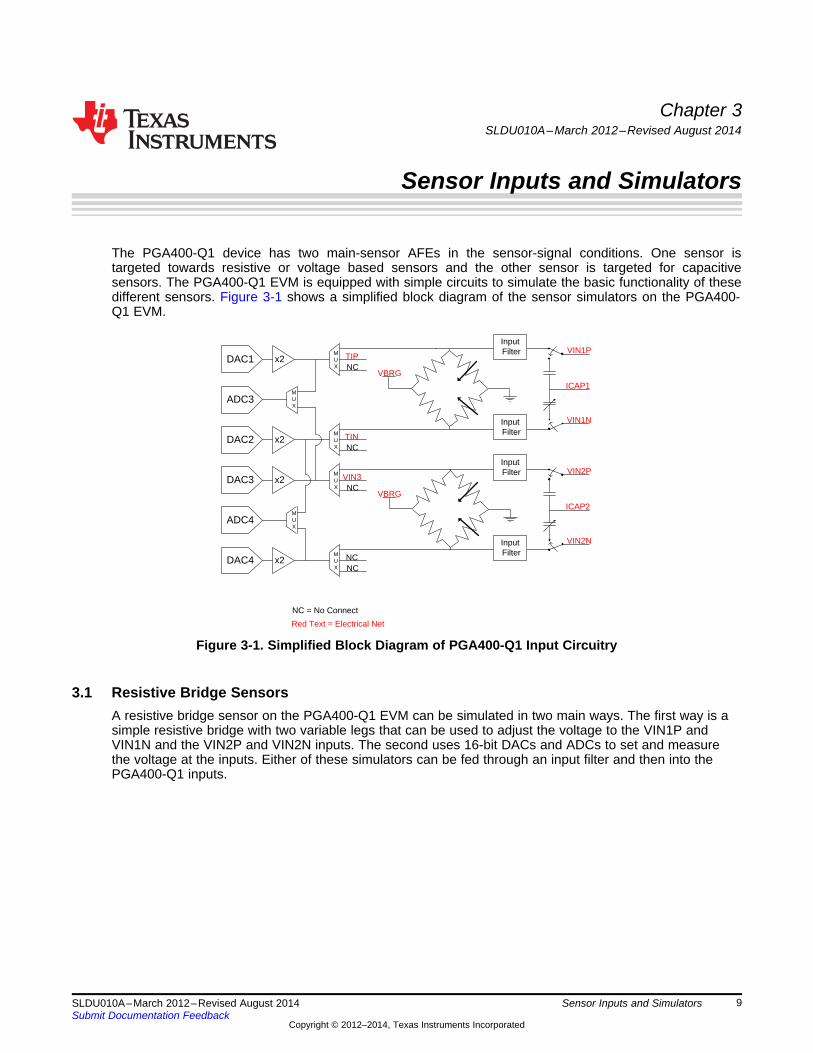
The PGA400-Q1 device has two main-sensor AFEs in the sensor-signal conditions. One sensor istargeted towards resistive or voltage based sensors and the other sensor is targeted for capacitivesensors. The PGA400-Q1 EVM is equipped with simple circuits to simulate the basic functionality of thesedifferent sensors. Figure 3-1 shows a simplified block diagram of the sensor simulators on the PGA400-Q1 EVM.
Figure 3-1. Simplified Block Diagram of PGA400-Q1 Input Circuitry
3.1 Resistive Bridge SensorsA resistive bridge sensor on the PGA400-Q1 EVM can be simulated in two main ways. The first way is asimple resistive bridge with two variable legs that can be used to adjust the voltage to the VIN1P andVIN1N and the VIN2P and VIN2N inputs. The second uses 16-bit DACs and ADCs to set and measurethe voltage at the inputs. Either of these simulators can be fed through an input filter and then into thePGA400-Q1 inputs.
9SLDU010A–March 2012–Revised August 2014 Sensor Inputs and SimulatorsSubmit Documentation Feedback
Copyright © 2012–2014, Texas Instruments Incorporated
R910k
R1010k
R177.5k
R187.5k
GND
VBRG
VIN1P_MB VIN1N_MB
5kR15 RPot
5kR14RPot
VIN1P_MB*R12
0.0R
VIN1N_MB*R13
0.0R
Resistive Bridge Sensors www.ti.com
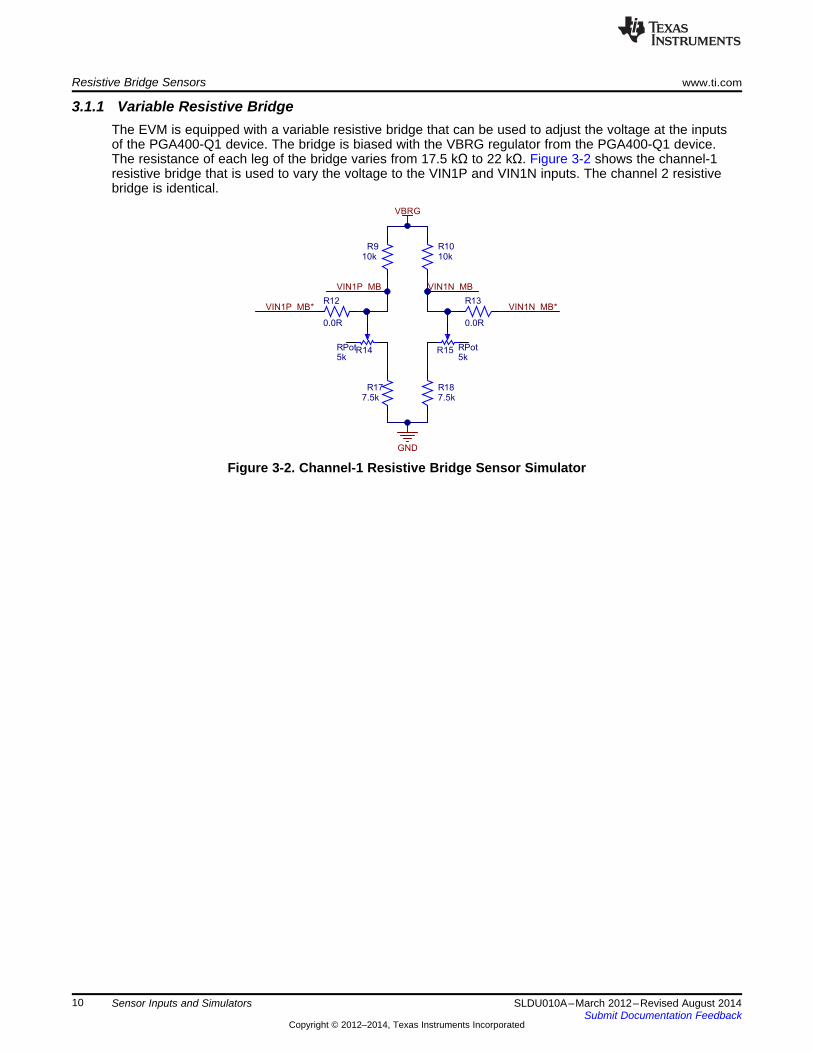
3.1.1 Variable Resistive BridgeThe EVM is equipped with a variable resistive bridge that can be used to adjust the voltage at the inputsof the PGA400-Q1 device. The bridge is biased with the VBRG regulator from the PGA400-Q1 device.The resistance of each leg of the bridge varies from 17.5 kΩ to 22 kΩ. Figure 3-2 shows the channel-1resistive bridge that is used to vary the voltage to the VIN1P and VIN1N inputs. The channel 2 resistivebridge is identical.
Figure 3-2. Channel-1 Resistive Bridge Sensor Simulator
10 Sensor Inputs and Simulators SLDU010A–March 2012–Revised August 2014Submit Documentation Feedback
Copyright © 2012–2014, Texas Instruments Incorporated
VOUTA1
VOUTB2
VREFH3
VD
D4
VREFL5
GN
D6
VOUTC7
VOUTD8
LDAC9
SCL10
SDA11
IOV
DD
12
A013
A114
A215
A416
U8DAC8574
GND
V5
12
C360.1uF,16V,X7R
GND
GND
DAC1_1DAC1_2DAC1_3DAC1_4
2
31
A
84
U5AOPA2335UA
GND
V5
R241k
5
67
B
84
U5BOPA2335UA
R251k
12
C351uF,16V,X7R
GND
V5
GND
GND
V5
R32
1k
R311k
GND
GND
V5
R361k R35
1k
12
C421uF,16V,X7R
GND
V5
GND
GND
V5
R401k R41
1k
GND
DAC1_1
DAC1_2
DAC1_3
DAC1_4
DAC1_1_BUF
DAC1_2_BUF
DAC1_3_BUF
DAC1_4_BUF
MB_SDAMB_SCL
1 2
C302.2nF,16V,X7R
1 2
C382.2nF,16V,X7R
1 2
C412.2nF,16V,X7R
1 2
C332.2nF,16V,X7R
V5
5
67
B
84
U10BOPA2335UA
2
31
A
84
U10AOPA2335UA
www.ti.com Resistive Bridge Sensors
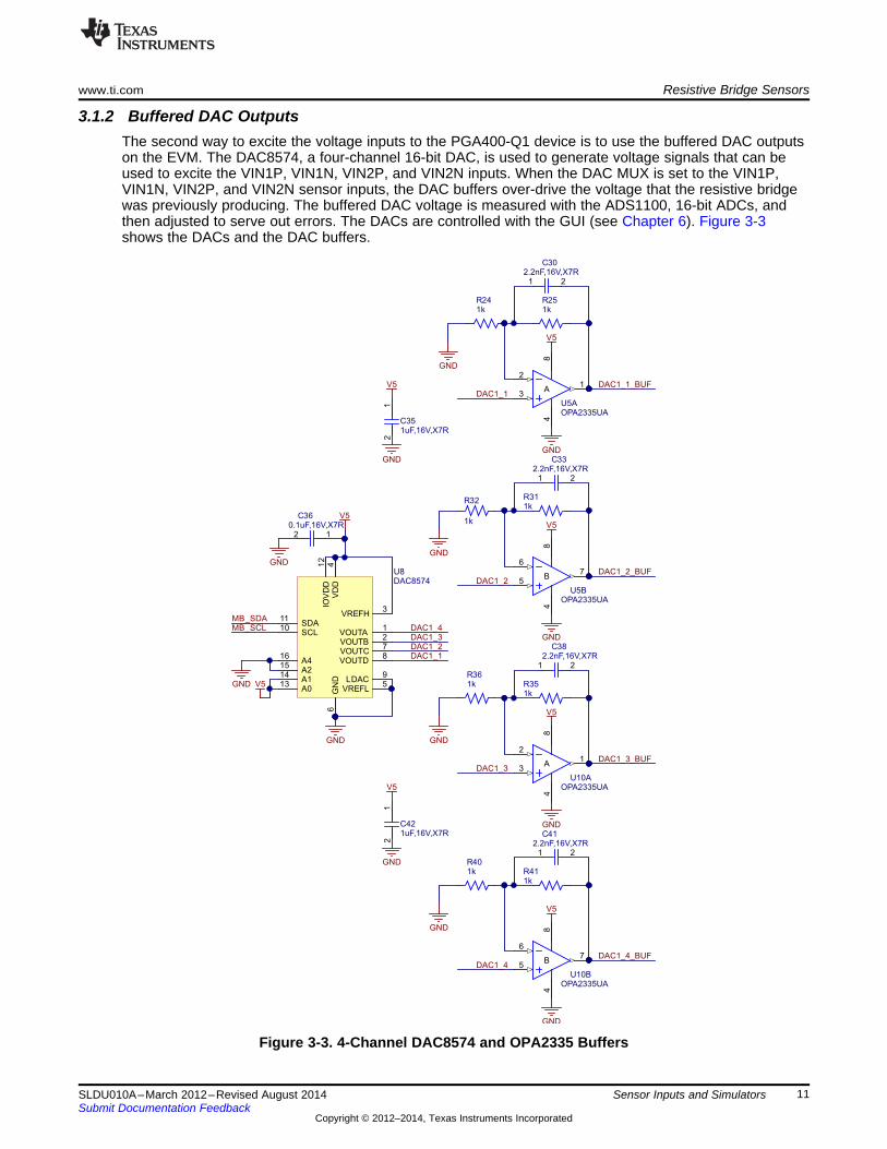
3.1.2 Buffered DAC OutputsThe second way to excite the voltage inputs to the PGA400-Q1 device is to use the buffered DAC outputson the EVM. The DAC8574, a four-channel 16-bit DAC, is used to generate voltage signals that can beused to excite the VIN1P, VIN1N, VIN2P, and VIN2N inputs. When the DAC MUX is set to the VIN1P,VIN1N, VIN2P, and VIN2N sensor inputs, the DAC buffers over-drive the voltage that the resistive bridgewas previously producing. The buffered DAC voltage is measured with the ADS1100, 16-bit ADCs, andthen adjusted to serve out errors. The DACs are controlled with the GUI (see Chapter 6). Figure 3-3shows the DACs and the DAC buffers.
Figure 3-3. 4-Channel DAC8574 and OPA2335 Buffers
11SLDU010A–March 2012–Revised August 2014 Sensor Inputs and SimulatorsSubmit Documentation Feedback
Copyright © 2012–2014, Texas Instruments Incorporated
JP17
JP19
JP10
JP12
VIN2P_C
VIN2N_C
VIN1P_C
VIN1N_C
VIN2P_R
VIN2N_R
VIN1P_R
VIN1N_R
VIN1P
VIN1N
VIN2P
VIN2N
12
C260.01uF
12
C310.01uF
12
C321nF
12
C281nF
12
C241nF
GND
GND
GND
12
C271nF
GND
JP16
JP18
JP11
JP9
VIN1P_MB
VIN1N_MB
VIN2P_MB
VIN2N_MB
C2510nF - X2Y
C2910nF - X2Y
GND GND
GND GND
L1
51R
L2
51R
L3
51R
L4
51R
DNI
DNI
51- Resistors are Installed Instead of Ferrite Beads L1 to L4. Remove the 51-Ω Ω resistors and replace with Ferrites if desired.
Resistive Bridge Sensors www.ti.com
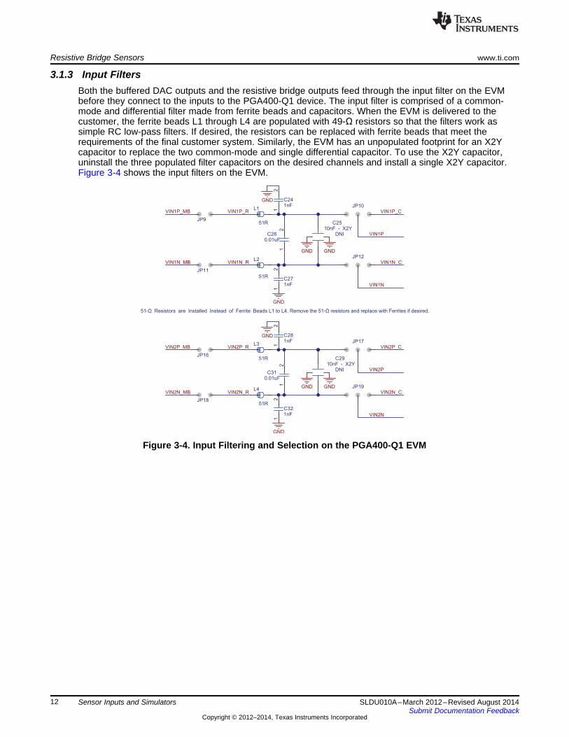
3.1.3 Input FiltersBoth the buffered DAC outputs and the resistive bridge outputs feed through the input filter on the EVMbefore they connect to the inputs to the PGA400-Q1 device. The input filter is comprised of a common-mode and differential filter made from ferrite beads and capacitors. When the EVM is delivered to thecustomer, the ferrite beads L1 through L4 are populated with 49-Ω resistors so that the filters work assimple RC low-pass filters. If desired, the resistors can be replaced with ferrite beads that meet therequirements of the final customer system. Similarly, the EVM has an unpopulated footprint for an X2Ycapacitor to replace the two common-mode and single differential capacitor. To use the X2Y capacitor,uninstall the three populated filter capacitors on the desired channels and install a single X2Y capacitor.Figure 3-4 shows the input filters on the EVM.
Figure 3-4. Input Filtering and Selection on the PGA400-Q1 EVM
12 Sensor Inputs and Simulators SLDU010A–March 2012–Revised August 2014Submit Documentation Feedback
Copyright © 2012–2014, Texas Instruments Incorporated
C1930pF
C2056pF
C2230pF
C2356pF
ICAP1
ICAP2
VIN2P_C
VIN2N_C
VIN1P_C
VIN1N_C
7.0-50pFC18
Cap Var
7.0-50pFC21
Cap Var
www.ti.com Capacitive Sensors
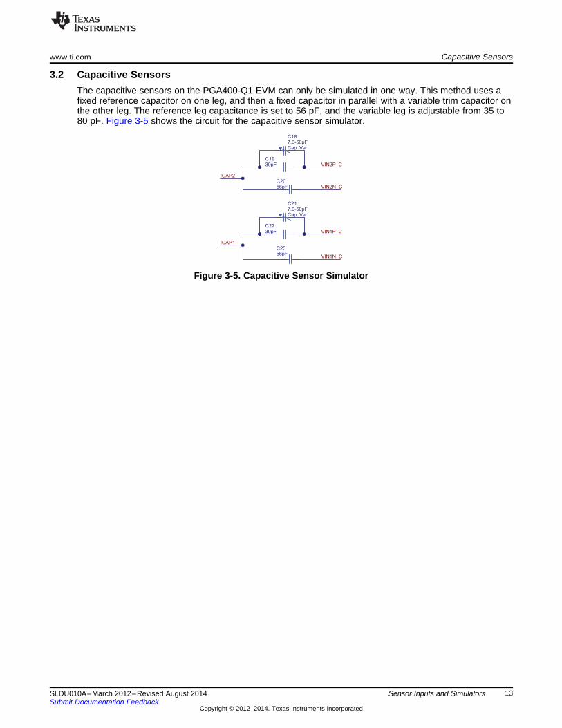
3.2 Capacitive SensorsThe capacitive sensors on the PGA400-Q1 EVM can only be simulated in one way. This method uses afixed reference capacitor on one leg, and then a fixed capacitor in parallel with a variable trim capacitor onthe other leg. The reference leg capacitance is set to 56 pF, and the variable leg is adjustable from 35 to80 pF. Figure 3-5 shows the circuit for the capacitive sensor simulator.
Figure 3-5. Capacitive Sensor Simulator
13SLDU010A–March 2012–Revised August 2014 Sensor Inputs and SimulatorsSubmit Documentation Feedback
Copyright © 2012–2014, Texas Instruments Incorporated
VOUT1NC
MUX
5 V
5 V
ADC1
USB-TX
USB-RX
7.5 V
5 V
OWI Activation
5R
49.9 k
49.9 k
200R
49.9 k
100 pF
VOUT1NC
MUX
ADC2
5 V
49.9 k
100 pF
Chapter 4SLDU010A–March 2012–Revised August 2014
PGA400-Q1 VOUT1 and VOUT2 Output Circuitry
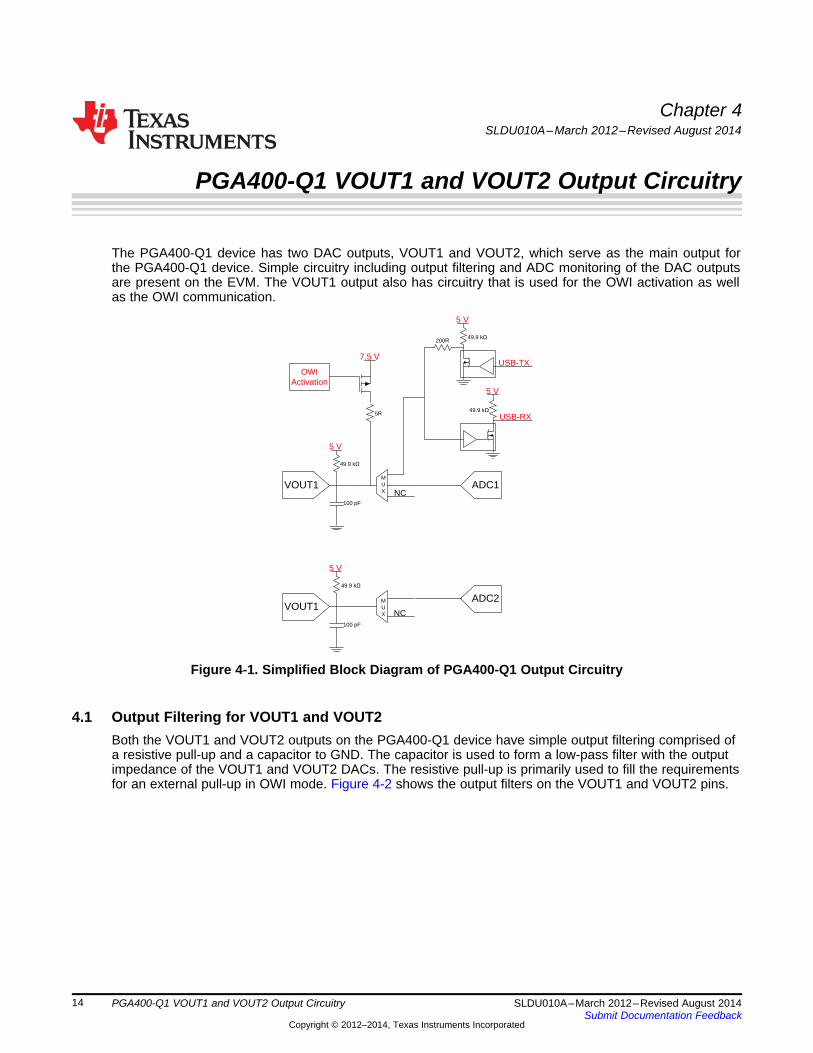
The PGA400-Q1 device has two DAC outputs, VOUT1 and VOUT2, which serve as the main output forthe PGA400-Q1 device. Simple circuitry including output filtering and ADC monitoring of the DAC outputsare present on the EVM. The VOUT1 output also has circuitry that is used for the OWI activation as wellas the OWI communication.
Figure 4-1. Simplified Block Diagram of PGA400-Q1 Output Circuitry
4.1 Output Filtering for VOUT1 and VOUT2Both the VOUT1 and VOUT2 outputs on the PGA400-Q1 device have simple output filtering comprised ofa resistive pull-up and a capacitor to GND. The capacitor is used to form a low-pass filter with the outputimpedance of the VOUT1 and VOUT2 DACs. The resistive pull-up is primarily used to fill the requirementsfor an external pull-up in OWI mode. Figure 4-2 shows the output filters on the VOUT1 and VOUT2 pins.
14 PGA400-Q1 VOUT1 and VOUT2 Output Circuitry SLDU010A–March 2012–Revised August 2014Submit Documentation Feedback
Copyright © 2012–2014, Texas Instruments Incorporated
Q3SI2319DS-T1-E3
R66
220k
R685R
R641k
GND
12
C59330nF,16V,X7R
GND
R6949.9k
GNDVOUT1_MB
V7p5_MB
Q42N2222
OWI_ACT
OWI_T
DZ45.1V Zener
DNI
12
C47
100pF,50V,,X7R
12
C44
100pF,50V,,X7R
GND
GND
VOUT1
VOUT2
R47
49k
R48
49k
V5
V5
JP23
JP22
VOUT1_MB
VOUT2_MB
www.ti.com ADC Measurement of VOUT1 and VOUT2 DAC Outputs
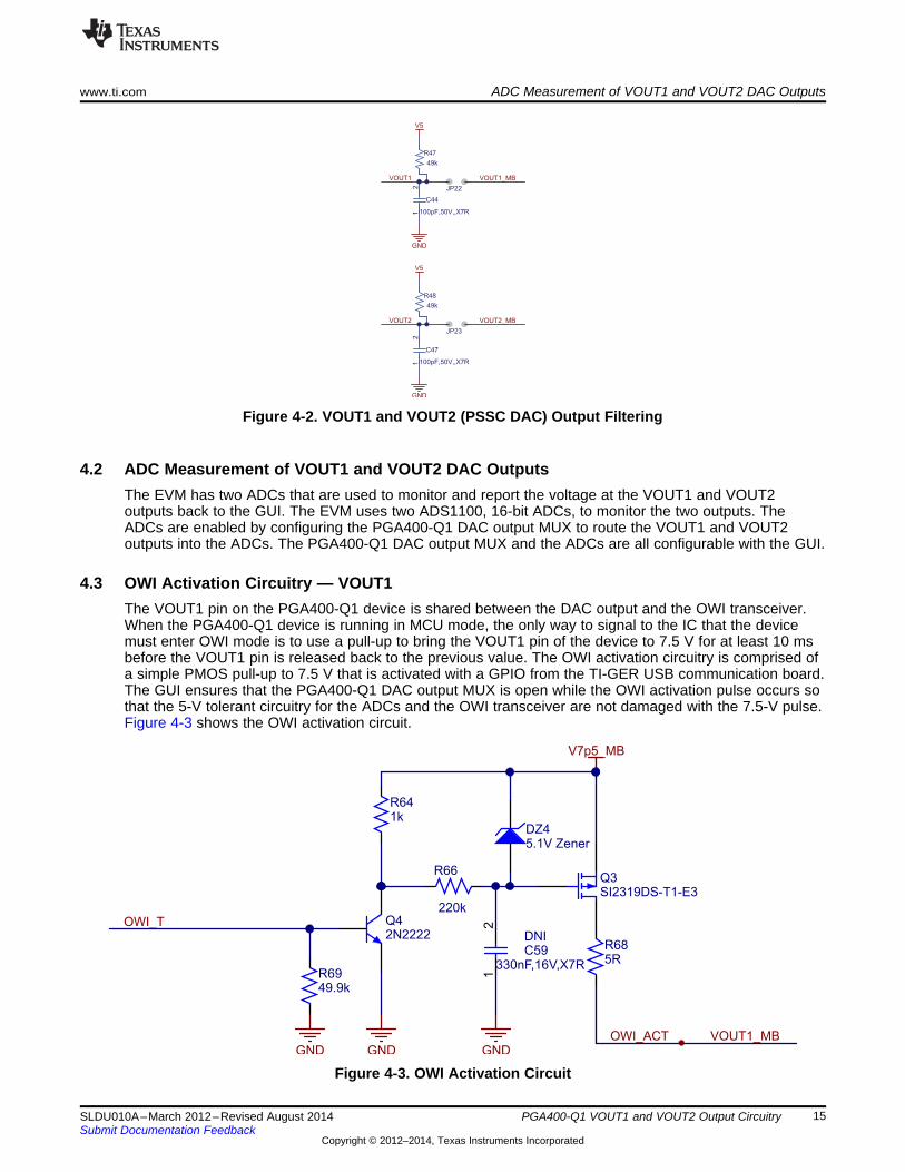
Figure 4-2. VOUT1 and VOUT2 (PSSC DAC) Output Filtering
4.2 ADC Measurement of VOUT1 and VOUT2 DAC OutputsThe EVM has two ADCs that are used to monitor and report the voltage at the VOUT1 and VOUT2outputs back to the GUI. The EVM uses two ADS1100, 16-bit ADCs, to monitor the two outputs. TheADCs are enabled by configuring the PGA400-Q1 DAC output MUX to route the VOUT1 and VOUT2outputs into the ADCs. The PGA400-Q1 DAC output MUX and the ADCs are all configurable with the GUI.
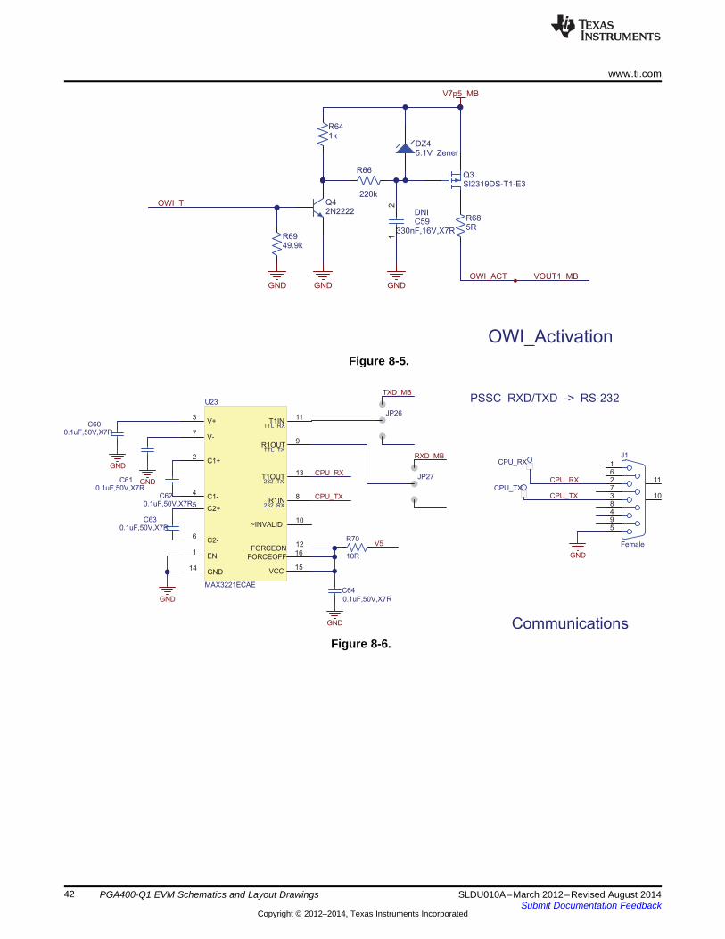
4.3 OWI Activation Circuitry — VOUT1The VOUT1 pin on the PGA400-Q1 device is shared between the DAC output and the OWI transceiver.When the PGA400-Q1 device is running in MCU mode, the only way to signal to the IC that the devicemust enter OWI mode is to use a pull-up to bring the VOUT1 pin of the device to 7.5 V for at least 10 msbefore the VOUT1 pin is released back to the previous value. The OWI activation circuitry is comprised ofa simple PMOS pull-up to 7.5 V that is activated with a GPIO from the TI-GER USB communication board.The GUI ensures that the PGA400-Q1 DAC output MUX is open while the OWI activation pulse occurs sothat the 5-V tolerant circuitry for the ADCs and the OWI transceiver are not damaged with the 7.5-V pulse.Figure 4-3 shows the OWI activation circuit.
Figure 4-3. OWI Activation Circuit
15SLDU010A–March 2012–Revised August 2014 PGA400-Q1 VOUT1 and VOUT2 Output CircuitrySubmit Documentation Feedback
Copyright © 2012–2014, Texas Instruments Incorporated
4
NC
13
5
2
U12SN74LVC1G07
GND
V5
R4449k
4
NC
13
5
2
U13SN74LVC1G07
R4549k
V5
GND
R46200R
TX
RX
OWI_TX_RX
TX
RX
OWI
OWI Transceiver — VOUT1 www.ti.com
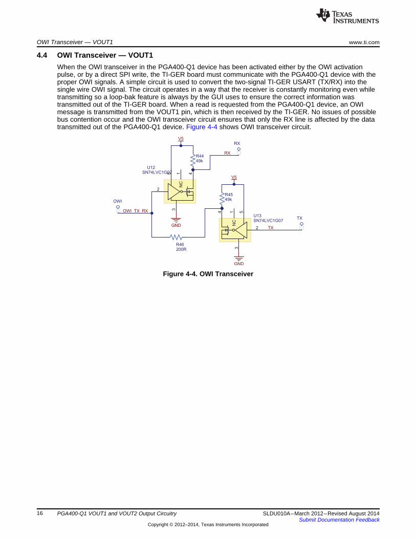
4.4 OWI Transceiver — VOUT1When the OWI transceiver in the PGA400-Q1 device has been activated either by the OWI activationpulse, or by a direct SPI write, the TI-GER board must communicate with the PGA400-Q1 device with theproper OWI signals. A simple circuit is used to convert the two-signal TI-GER USART (TX/RX) into thesingle wire OWI signal. The circuit operates in a way that the receiver is constantly monitoring even whiletransmitting so a loop-bak feature is always by the GUI uses to ensure the correct information wastransmitted out of the TI-GER board. When a read is requested from the PGA400-Q1 device, an OWImessage is transmitted from the VOUT1 pin, which is then received by the TI-GER. No issues of possiblebus contention occur and the OWI transceiver circuit ensures that only the RX line is affected by the datatransmitted out of the PGA400-Q1 device. Figure 4-4 shows OWI transceiver circuit.
Figure 4-4. OWI Transceiver
16 PGA400-Q1 VOUT1 and VOUT2 Output Circuitry SLDU010A–March 2012–Revised August 2014Submit Documentation Feedback
Copyright © 2012–2014, Texas Instruments Incorporated
SCLK_T
MOSI_TMISO_TSDA
SCLK_MBR7649.9k
GND
4B114
S1
1B12
4B213
1B23
1A4
3A9
2B26
2B15
4A12
GND8
2A7
3B111
VCC16
3B210
OE15
U26
SN74CBTLV3257
V51 2
C680.1uF.16V,X7R
GND
SPI/I2C
CS_TMISO_MBMOSI_MB
CS_MBSCL
GND
R7849.9k
GNDR79
49.9k
GND
R7749.9k
COMM_EN
GND
Chapter 5SLDU010A–March 2012–Revised August 2014
PGA400-Q1 Communication Interfaces
The PGA400-Q1 device has several communication options including: SPI, I2C, OWI, and UART. All ofthese communication interfaces and related circuitry are present on the PGA400-Q1 EVM.
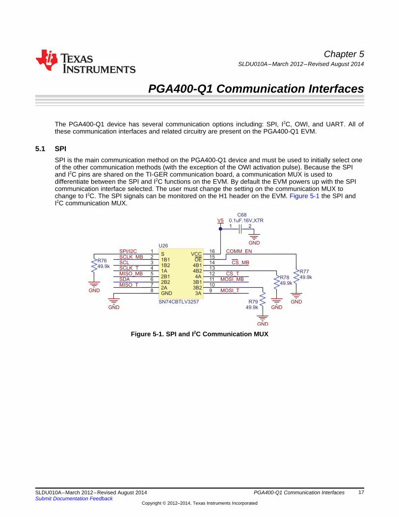
5.1 SPISPI is the main communication method on the PGA400-Q1 device and must be used to initially select oneof the other communication methods (with the exception of the OWI activation pulse). Because the SPIand I2C pins are shared on the TI-GER communication board, a communication MUX is used todifferentiate between the SPI and I2C functions on the EVM. By default the EVM powers up with the SPIcommunication interface selected. The user must change the setting on the communication MUX tochange to I2C. The SPI signals can be monitored on the H1 header on the EVM. Figure 5-1 the SPI andI2C communication MUX.
Figure 5-1. SPI and I2C Communication MUX
17SLDU010A–March 2012–Revised August 2014 PGA400-Q1 Communication InterfacesSubmit Documentation Feedback
Copyright © 2012–2014, Texas Instruments Incorporated
NC19
COM110
NO12
V+8
GND3
NC27
COM26
NO24
IN25
IN11
U27
TS5A23159
V51 2
C690.1uF.16V,X7R
GND
GND
SDA
SCL
SDA_PSSC
SCL_PSSCI2C_MB/PSSC
R8049.9k
GND
MB_SDA
MB_SCL
I2C www.ti.com
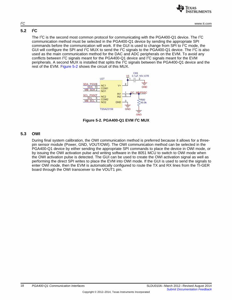
5.2 I2CThe I2C is the second most common protocol for communicating with the PGA400-Q1 device. The I2Ccommunication method must be selected in the PGA400-Q1 device by sending the appropriate SPIcommands before the communication will work. If the GUI is used to change from SPI to I2C mode, theGUI will configure the SPI and I2C MUX to send the I2C signals to the PGA400-Q1 device. The I2C is alsoused as the main communication method for the DAC and ADC peripherals on the EVM. To avoid anyconflicts between I2C signals meant for the PGA400-Q1 device and I2C signals meant for the EVMperipherals. A second MUX is installed that splits the I2C signals between the PGA400-Q1 device and therest of the EVM. Figure 5-2 shows the circuit of this MUX.
Figure 5-2. PGA400-Q1 EVM I2C MUX
5.3 OWIDuring final system calibration, the OWI communication method is preferred because it allows for a three-pin sensor module (Power, GND, VOUT/OWI). The OWI communication method can be selected in thePGA400-Q1 device by either sending the appropriate SPI commands to place the device in OWI mode, orby issuing the OWI activation pulse and writing software in the 8051 MCU to switch to OWI mode whenthe OWI activation pulse is detected. The GUI can be used to create the OWI activation signal as well asperforming the direct SPI writes to place the EVM into OWI mode. If the GUI is used to send the signals toenter OWI mode, then the EVM is automatically configured to route the TX and RX lines from the TI-GERboard through the OWI transceiver to the VOUT1 pin.
18 PGA400-Q1 Communication Interfaces SLDU010A–March 2012–Revised August 2014Submit Documentation Feedback
Copyright © 2012–2014, Texas Instruments Incorporated
C620.1uF,50V,X7R
C630.1uF,50V,X7R
C600.1uF,50V,X7R
C610.1uF,50V,X7R
C64
0.1uF,50V,X7R
CPU_TX
CPU_RX
1
2
3
4
5
6
7
8
9
11
10
J1
Female
CPU_TX
CPU_RX
CPU_RX
CPU_TX
GND
GND
GND
GND
GND
V5
C1+2
C1-4
C2+5
C2-6
T1IN11
R1OUT9
EN1
FORCEON12
GND14
V+3
V-7
T1OUT13
R1IN8
VCC15
FORCEOFF16
~INVALID10
232 TX
TTL TX
TTL RX
232 RX
U23
MAX3221ECAE
R70
10R
RXD_MB
TXD_MB
JP26
JP27
www.ti.com UART
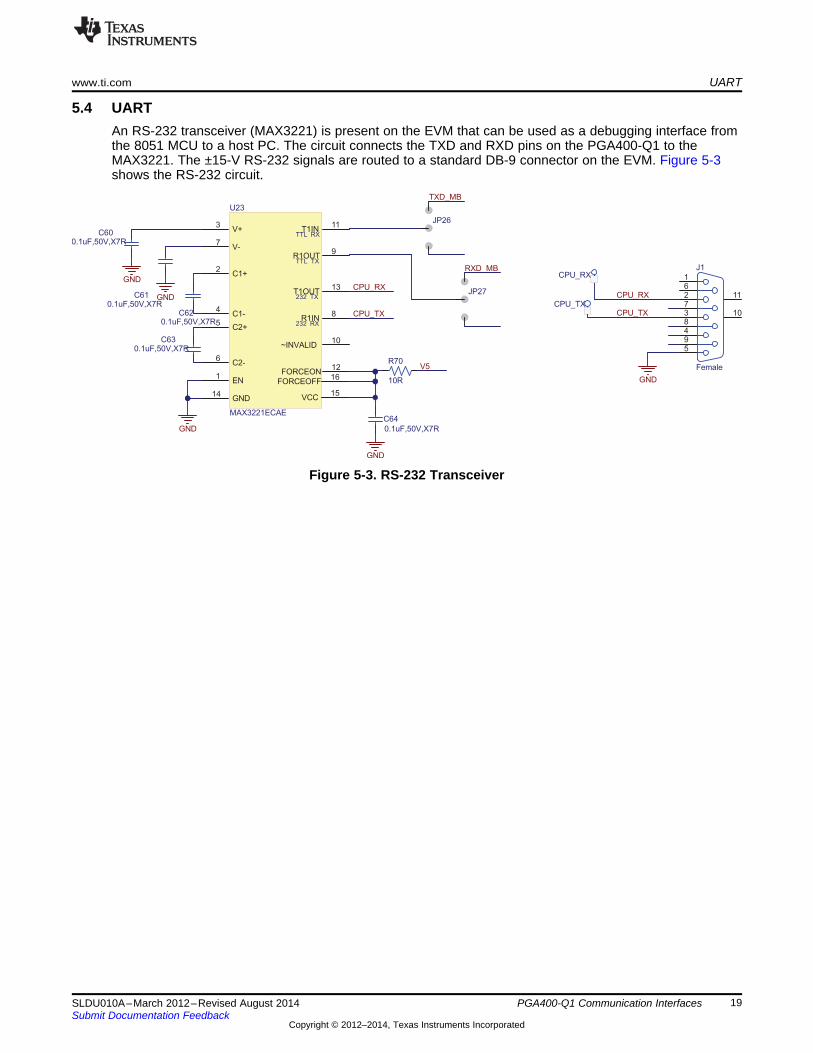
5.4 UARTAn RS-232 transceiver (MAX3221) is present on the EVM that can be used as a debugging interface fromthe 8051 MCU to a host PC. The circuit connects the TXD and RXD pins on the PGA400-Q1 to theMAX3221. The ±15-V RS-232 signals are routed to a standard DB-9 connector on the EVM. Figure 5-3shows the RS-232 circuit.
Figure 5-3. RS-232 Transceiver
19SLDU010A–March 2012–Revised August 2014 PGA400-Q1 Communication InterfacesSubmit Documentation Feedback
Copyright © 2012–2014, Texas Instruments Incorporated
Chapter 6SLDU010A–March 2012–Revised August 2014
Controlling the PGA400-Q1 Memory Spaces with the GUI
The PGA400-Q1 EVM is controlled by the user through a PC with the TI-GER USB communication boardand associated GUI. The PGA400-Q1 EVM GUI provides ways to manipulate all of the register spacespresent inside the PGA400-Q1 device (TEST, ESFR, EEPROM, IRAM, OTP). The following sectionsdescribe how to manipulate the register spaces.
6.1 Using the Register Grids to Manipulate the Register SpacesMost of the register spaces have register grids associated with them that provide a simple way to read,write, or read and write the registers in the grid. Eight buttons are associated with the grid operations:ZERO GRID, DESELECT GRID, SAVE GRID, RECALL GRID, READ SELECTED, WRITE SELECTED,READ ALL, and WRITE ALL. These buttons perform operations on whichever register grid is currentlydisplayed. For example, when the GUI first loads, the TEST register tab is displayed. If any of thepreviously listed buttons are pressed the buttons perform operations on the TEST register space. Thefollowing sections describe each of the grid functions.
6.1.1 ZERO GRIDThe ZERO GRID button replaces the contents of the entire grid with 0.
6.1.2 DESELECT GRIDThe DESELECT GRID button removes any selections that have been made in the grid without performingany operations on the registers that were selected.
6.1.3 SAVE GRIDThe SAVE GRID button takes the contents of the register grid and save them to a .TXT file. The data issaved in comma-separated-values format.
6.1.4 RECALL GRIDThe RECALL GRID button opens a prompt that allows the user to select a .TXT file that was producedduring the SAVE GRID operation and then loads the grid with the contents from the .TXT file.
6.1.5 READ SELECTEDThe READ SELECTED button performs a read operation on any registers in the grid that have beenselected by clicking the desired register number. Any selected registers are displayed in blue.
6.1.6 WRITE SELECTEDThe WRITE SELECTED button performs a write operation on any registers in the grid that have beenselected by clicking the register number or modifying the register contents. Any selected registers aredisplayed in blue and any modified registers are displayed in yellow. Any blue or yellow registers arewritten to when the WRITE SELECTED button is pressed.
6.1.7 READ ALLThe READ ALL button performs a read operation on every register in the grid.
20 Controlling the PGA400-Q1 Memory Spaces with the GUI SLDU010A–March 2012–Revised August 2014Submit Documentation Feedback
Copyright © 2012–2014, Texas Instruments Incorporated
www.ti.com Using the Register Grids to Manipulate the Register Spaces
6.1.8 WRITE ALLThe WRITE ALL button performs a write operation on every register in the grid.
6.2 Test RegistersBy default, the GUI opens with the TEST register-grid displayed. Aside from the functions associateddirectly with the grid, the TEST tab includes two buttons related to the TEST registers.
6.2.1 IFSEL/uC_RSTThe IFSEL/uC_RST button toggles bit 0 and bit 1 of register 0x0E. Press this button to select SPI andshutdown the 8051 MCU before most other commands on the GUI will take affect is required.
6.2.2 Restricted AccessAs described in the PGA400-Q1 data sheet (SLDS186), in order to access some of the features in theTEST register map, a special unlock sequence must be sent to register 0xFF. The Restricted Accessbutton sends this sequence to the PGA400-Q1 device.
6.3 ESFR RegistersThe ESFR register tab only contains a grid that can be used with the functions described before to directlymanipulate the ESFR register space. Most of the buttons on the right half of the GUI control bits in theESFR register tab. These buttons are described in Chapter 7.
6.4 EEPROM RegistersThe EEPROM in the PGA400-Q1 device is comprised of six banks of EEPROM (BANK_0 to BANK_5)and a shared cache. In the PGA400-Q1 GUI, each EEPROM BANK is given a grid even though alloperations are performed on the shared cache. As before, whichever BANK tab is displayed is theEEPROM bank that is operated on which is achieved by updating the EEPROM bank select bits in theTEST register space when the user selects a different EEPROM tab. By default, BANK_0 is selected. Thefour buttons on the EEPROM tab are described in the following sections.
6.4.1 Auto Program EEPROMThe Auto Program EEPROM button uses the internal EEPROM charge pump and timer to enable andthen disable the EEPROM charge pump after the programming time has been met. This button should beused if the user desires to burn the current EEPROM cache contents to the EEPROM bank.
6.4.2 PROG_ONThe PROG_ON button is used for a manual method of programming/testing the EEPROM. ThePROG_ON button turns on the EEPROM charge pump. Because no timer exists to automatically turn theEEPROM charge pump back off, the user must press the PROG_OFF button to disable the charge-pump
6.4.3 PROG_OFFThe PROG_OFF button is used to complete a manual EEPROM programming by disabling the EEPROMcharge pump.
6.4.4 Reload CACHEThe Reload CACHE button uses the TEST register 0x0D to reload the CACHE with the contents of theselected EEPROM bank and then performs a read-all to update the grid with the refreshed contents of theEEPROM bank.
21SLDU010A–March 2012–Revised August 2014 Controlling the PGA400-Q1 Memory Spaces with the GUISubmit Documentation Feedback
Copyright © 2012–2014, Texas Instruments Incorporated
IRAM www.ti.com
6.5 IRAMThe IRAM tab is setup only for individual register read and writes without the use of the grid. When thistab is displayed, the READ SELECTED / READ ALL and WRITE SELECTED / WRITE ALL buttonsperform the same operations respectively.
6.6 OTPThe OTP tab is setup only for individual register read/writes without the use of the grid. When this tab isdisplayed, the READ SELECTED, READ ALL, WRITE SELECTED, and WRITE ALL buttons perform thesame operations respectively. The OTP tab also contains buttons used to load a .HEX 8051 program fileinto the 8051 MCU in the PGA400-Q1 device.
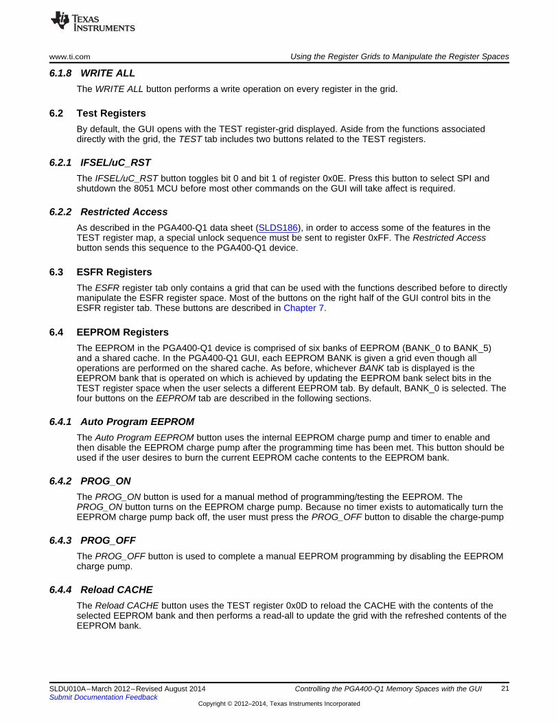
6.6.1 Load .HEX File into GUIThe Load .HEX File into GUI button is used to load the contents of a .HEX file into the GUI RAM for usewith other operations. When the button is pressed, a second window opens that allows the user to locateand open the desired .HEX file on the PC. Figure 6-1 shows an example of this operation.
Figure 6-1. Loading a .HEX File into the GUI
6.6.2 Program OTP Memory from .HEX FileIf the Program OTP Memory from .HEX File check box was checked (default) when the .HEX file wasloaded into the GUI, the OTP memory is programmed with the contents of the .HEX file.
22 Controlling the PGA400-Q1 Memory Spaces with the GUI SLDU010A–March 2012–Revised August 2014Submit Documentation Feedback
Copyright © 2012–2014, Texas Instruments Incorporated
www.ti.com OTP
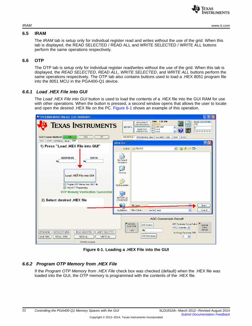
6.6.3 Verify OTP ProgrammingIf the Verify OTP Programming button was also checked (default) then after the OTP memory is finishedprogramming, the GUI resets the MCU and then verifies that the contents of the OTP memory match the.HEX file. If the OTP memory matches the contents of the .HEX file, the GUI displays the message OTPMemory Verification Successful as shown in green text in Figure 6-2.
Figure 6-2. OTP Memory Successful Programming Verification
23SLDU010A–March 2012–Revised August 2014 Controlling the PGA400-Q1 Memory Spaces with the GUISubmit Documentation Feedback
Copyright © 2012–2014, Texas Instruments Incorporated
Chapter 7SLDU010A–March 2012–Revised August 2014
Controlling the PGA400-Q1 Functions with the GUI
The previous section focused on the left side of the GUI which is primarily used for direct registermanipulation. The right side of the GUI is focused on providing a graphical method for controlling thePGA400-Q1 device.
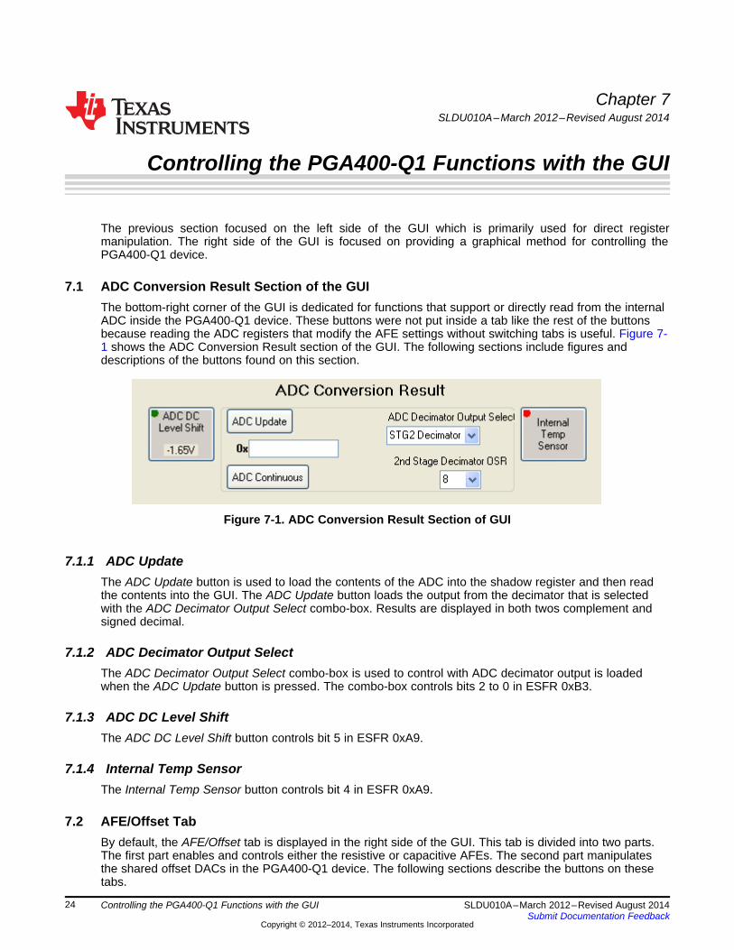
7.1 ADC Conversion Result Section of the GUIThe bottom-right corner of the GUI is dedicated for functions that support or directly read from the internalADC inside the PGA400-Q1 device. These buttons were not put inside a tab like the rest of the buttonsbecause reading the ADC registers that modify the AFE settings without switching tabs is useful. Figure 7-1 shows the ADC Conversion Result section of the GUI. The following sections include figures anddescriptions of the buttons found on this section.
Figure 7-1. ADC Conversion Result Section of GUI
7.1.1 ADC UpdateThe ADC Update button is used to load the contents of the ADC into the shadow register and then readthe contents into the GUI. The ADC Update button loads the output from the decimator that is selectedwith the ADC Decimator Output Select combo-box. Results are displayed in both twos complement andsigned decimal.
7.1.2 ADC Decimator Output SelectThe ADC Decimator Output Select combo-box is used to control with ADC decimator output is loadedwhen the ADC Update button is pressed. The combo-box controls bits 2 to 0 in ESFR 0xB3.
7.1.3 ADC DC Level ShiftThe ADC DC Level Shift button controls bit 5 in ESFR 0xA9.
7.1.4 Internal Temp SensorThe Internal Temp Sensor button controls bit 4 in ESFR 0xA9.
7.2 AFE/Offset TabBy default, the AFE/Offset tab is displayed in the right side of the GUI. This tab is divided into two parts.The first part enables and controls either the resistive or capacitive AFEs. The second part manipulatesthe shared offset DACs in the PGA400-Q1 device. The following sections describe the buttons on thesetabs.
24 Controlling the PGA400-Q1 Functions with the GUI SLDU010A–March 2012–Revised August 2014Submit Documentation Feedback
Copyright © 2012–2014, Texas Instruments Incorporated
www.ti.com AFE/Offset Tab
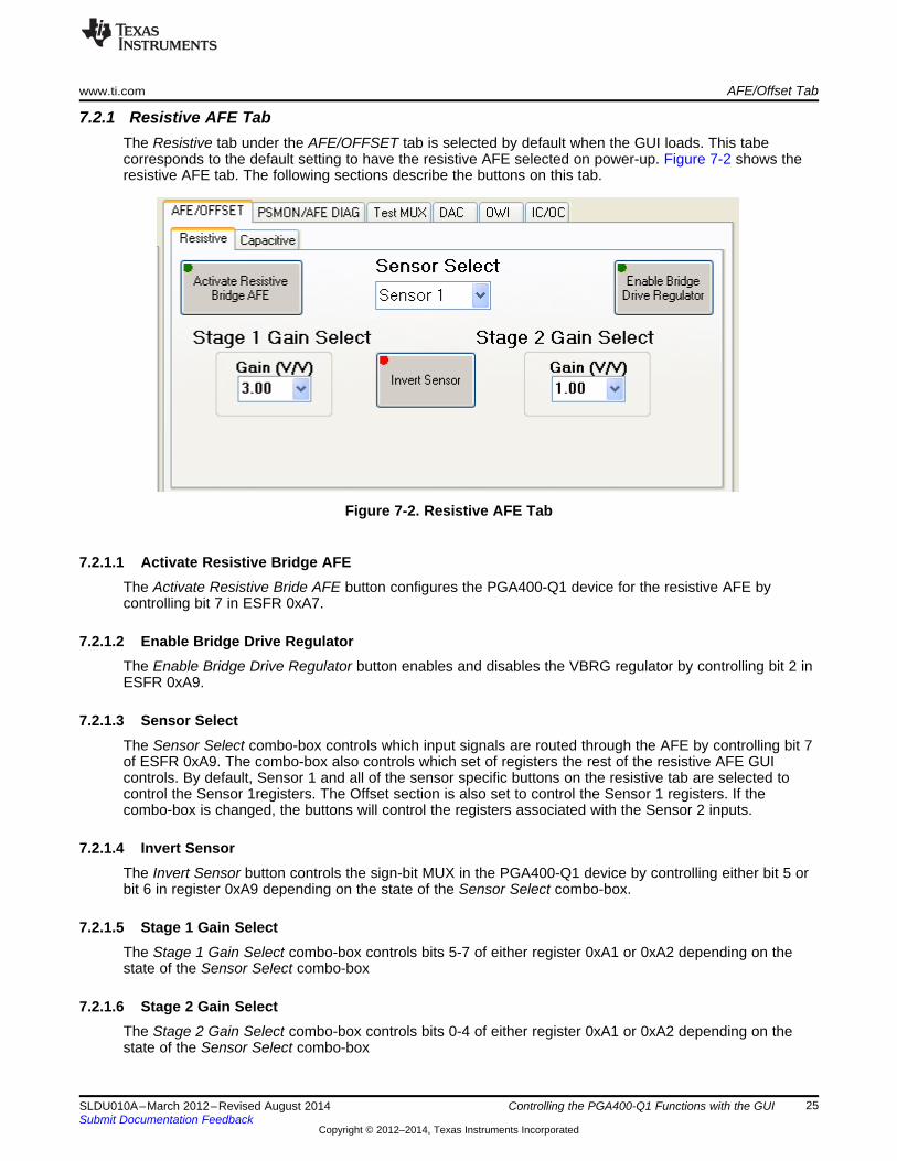
7.2.1 Resistive AFE TabThe Resistive tab under the AFE/OFFSET tab is selected by default when the GUI loads. This tabecorresponds to the default setting to have the resistive AFE selected on power-up. Figure 7-2 shows theresistive AFE tab. The following sections describe the buttons on this tab.
Figure 7-2. Resistive AFE Tab
7.2.1.1 Activate Resistive Bridge AFEThe Activate Resistive Bride AFE button configures the PGA400-Q1 device for the resistive AFE bycontrolling bit 7 in ESFR 0xA7.
7.2.1.2 Enable Bridge Drive RegulatorThe Enable Bridge Drive Regulator button enables and disables the VBRG regulator by controlling bit 2 inESFR 0xA9.
7.2.1.3 Sensor SelectThe Sensor Select combo-box controls which input signals are routed through the AFE by controlling bit 7of ESFR 0xA9. The combo-box also controls which set of registers the rest of the resistive AFE GUIcontrols. By default, Sensor 1 and all of the sensor specific buttons on the resistive tab are selected tocontrol the Sensor 1registers. The Offset section is also set to control the Sensor 1 registers. If thecombo-box is changed, the buttons will control the registers associated with the Sensor 2 inputs.
7.2.1.4 Invert SensorThe Invert Sensor button controls the sign-bit MUX in the PGA400-Q1 device by controlling either bit 5 orbit 6 in register 0xA9 depending on the state of the Sensor Select combo-box.
7.2.1.5 Stage 1 Gain SelectThe Stage 1 Gain Select combo-box controls bits 5-7 of either register 0xA1 or 0xA2 depending on thestate of the Sensor Select combo-box
7.2.1.6 Stage 2 Gain SelectThe Stage 2 Gain Select combo-box controls bits 0-4 of either register 0xA1 or 0xA2 depending on thestate of the Sensor Select combo-box
25SLDU010A–March 2012–Revised August 2014 Controlling the PGA400-Q1 Functions with the GUISubmit Documentation Feedback
Copyright © 2012–2014, Texas Instruments Incorporated
AFE/Offset Tab www.ti.com
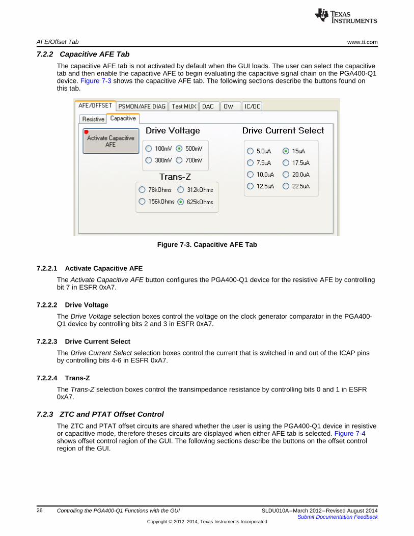
7.2.2 Capacitive AFE TabThe capacitive AFE tab is not activated by default when the GUI loads. The user can select the capacitivetab and then enable the capacitive AFE to begin evaluating the capacitive signal chain on the PGA400-Q1device. Figure 7-3 shows the capacitive AFE tab. The following sections describe the buttons found onthis tab.
Figure 7-3. Capacitive AFE Tab
7.2.2.1 Activate Capacitive AFEThe Activate Capacitive AFE button configures the PGA400-Q1 device for the resistive AFE by controllingbit 7 in ESFR 0xA7.
7.2.2.2 Drive VoltageThe Drive Voltage selection boxes control the voltage on the clock generator comparator in the PGA400-Q1 device by controlling bits 2 and 3 in ESFR 0xA7.
7.2.2.3 Drive Current SelectThe Drive Current Select selection boxes control the current that is switched in and out of the ICAP pinsby controlling bits 4-6 in ESFR 0xA7.
7.2.2.4 Trans-ZThe Trans-Z selection boxes control the transimpedance resistance by controlling bits 0 and 1 in ESFR0xA7.
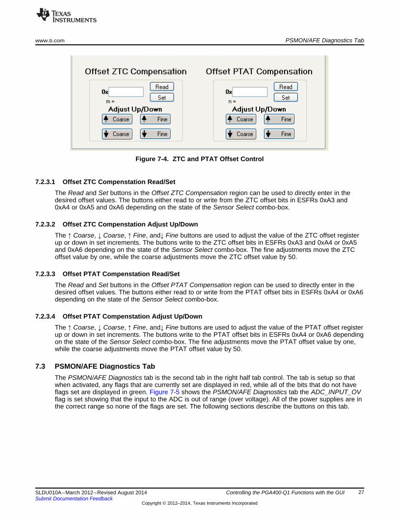
7.2.3 ZTC and PTAT Offset ControlThe ZTC and PTAT offset circuits are shared whether the user is using the PGA400-Q1 device in resistiveor capacitive mode, therefore theses circuits are displayed when either AFE tab is selected. Figure 7-4shows offset control region of the GUI. The following sections describe the buttons on the offset controlregion of the GUI.
26 Controlling the PGA400-Q1 Functions with the GUI SLDU010A–March 2012–Revised August 2014Submit Documentation Feedback
Copyright © 2012–2014, Texas Instruments Incorporated
www.ti.com PSMON/AFE Diagnostics Tab
Figure 7-4. ZTC and PTAT Offset Control
7.2.3.1 Offset ZTC Compenstation Read/SetThe Read and Set buttons in the Offset ZTC Compensation region can be used to directly enter in thedesired offset values. The buttons either read to or write from the ZTC offset bits in ESFRs 0xA3 and0xA4 or 0xA5 and 0xA6 depending on the state of the Sensor Select combo-box.
7.2.3.2 Offset ZTC Compenstation Adjust Up/DownThe ↑ Coarse, ↓ Coarse, ↑ Fine, and↓ Fine buttons are used to adjust the value of the ZTC offset registerup or down in set increments. The buttons write to the ZTC offset bits in ESFRs 0xA3 and 0xA4 or 0xA5and 0xA6 depending on the state of the Sensor Select combo-box. The fine adjustments move the ZTCoffset value by one, while the coarse adjustments move the ZTC offset value by 50.
7.2.3.3 Offset PTAT Compenstation Read/SetThe Read and Set buttons in the Offset PTAT Compensation region can be used to directly enter in thedesired offset values. The buttons either read to or write from the PTAT offset bits in ESFRs 0xA4 or 0xA6depending on the state of the Sensor Select combo-box.
7.2.3.4 Offset PTAT Compenstation Adjust Up/DownThe ↑ Coarse, ↓ Coarse, ↑ Fine, and↓ Fine buttons are used to adjust the value of the PTAT offset registerup or down in set increments. The buttons write to the PTAT offset bits in ESFRs 0xA4 or 0xA6 dependingon the state of the Sensor Select combo-box. The fine adjustments move the PTAT offset value by one,while the coarse adjustments move the PTAT offset value by 50.
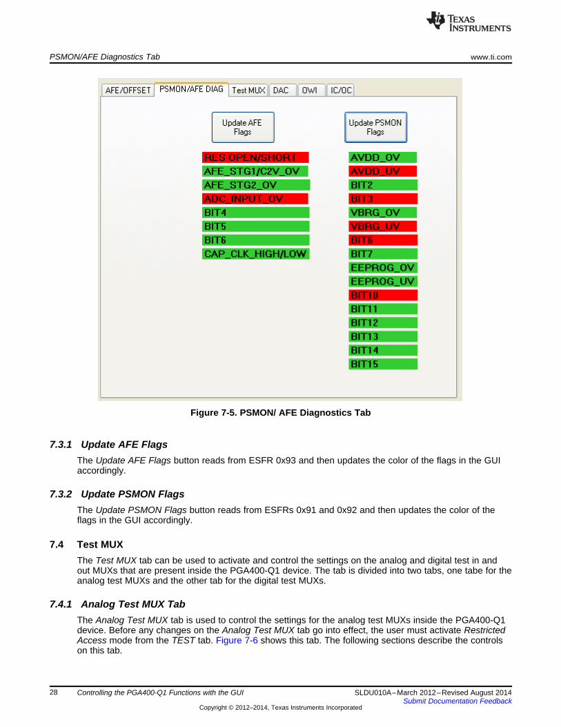
7.3 PSMON/AFE Diagnostics TabThe PSMON/AFE Diagnostics tab is the second tab in the right half tab control. The tab is setup so thatwhen activated, any flags that are currently set are displayed in red, while all of the bits that do not haveflags set are displayed in green. Figure 7-5 shows the PSMON/AFE Diagnostics tab the ADC_INPUT_OVflag is set showing that the input to the ADC is out of range (over voltage). All of the power supplies are inthe correct range so none of the flags are set. The following sections describe the buttons on this tab.
27SLDU010A–March 2012–Revised August 2014 Controlling the PGA400-Q1 Functions with the GUISubmit Documentation Feedback
Copyright © 2012–2014, Texas Instruments Incorporated
PSMON/AFE Diagnostics Tab www.ti.com
Figure 7-5. PSMON/ AFE Diagnostics Tab
7.3.1 Update AFE FlagsThe Update AFE Flags button reads from ESFR 0x93 and then updates the color of the flags in the GUIaccordingly.
7.3.2 Update PSMON FlagsThe Update PSMON Flags button reads from ESFRs 0x91 and 0x92 and then updates the color of theflags in the GUI accordingly.
7.4 Test MUXThe Test MUX tab can be used to activate and control the settings on the analog and digital test in andout MUXs that are present inside the PGA400-Q1 device. The tab is divided into two tabs, one tabe for theanalog test MUXs and the other tab for the digital test MUXs.
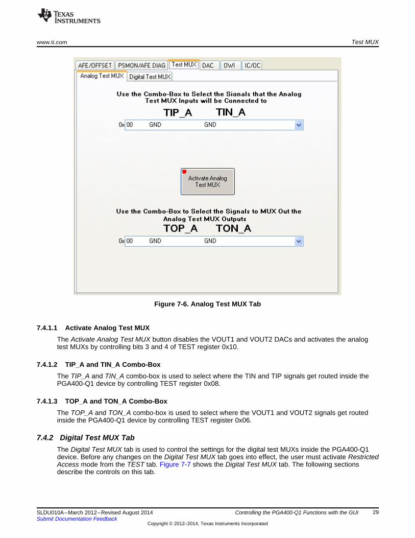
7.4.1 Analog Test MUX TabThe Analog Test MUX tab is used to control the settings for the analog test MUXs inside the PGA400-Q1device. Before any changes on the Analog Test MUX tab go into effect, the user must activate RestrictedAccess mode from the TEST tab. Figure 7-6 shows this tab. The following sections describe the controlson this tab.
28 Controlling the PGA400-Q1 Functions with the GUI SLDU010A–March 2012–Revised August 2014Submit Documentation Feedback
Copyright © 2012–2014, Texas Instruments Incorporated
www.ti.com Test MUX
Figure 7-6. Analog Test MUX Tab
7.4.1.1 Activate Analog Test MUXThe Activate Analog Test MUX button disables the VOUT1 and VOUT2 DACs and activates the analogtest MUXs by controlling bits 3 and 4 of TEST register 0x10.
7.4.1.2 TIP_A and TIN_A Combo-BoxThe TIP_A and TIN_A combo-box is used to select where the TIN and TIP signals get routed inside thePGA400-Q1 device by controlling TEST register 0x08.
7.4.1.3 TOP_A and TON_A Combo-BoxThe TOP_A and TON_A combo-box is used to select where the VOUT1 and VOUT2 signals get routedinside the PGA400-Q1 device by controlling TEST register 0x06.
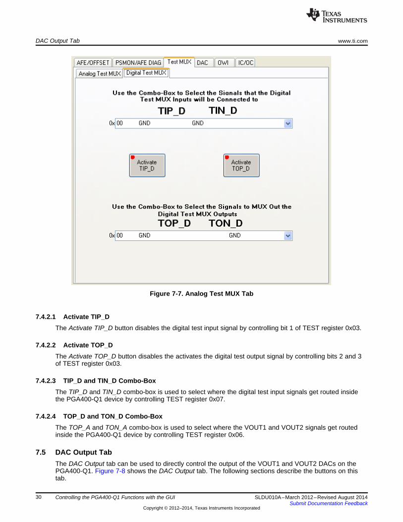
7.4.2 Digital Test MUX TabThe Digital Test MUX tab is used to control the settings for the digital test MUXs inside the PGA400-Q1device. Before any changes on the Digital Test MUX tab goes into effect, the user must activate RestrictedAccess mode from the TEST tab. Figure 7-7 shows the Digital Test MUX tab. The following sectionsdescribe the controls on this tab.
29SLDU010A–March 2012–Revised August 2014 Controlling the PGA400-Q1 Functions with the GUISubmit Documentation Feedback
Copyright © 2012–2014, Texas Instruments Incorporated
DAC Output Tab www.ti.com
Figure 7-7. Analog Test MUX Tab
7.4.2.1 Activate TIP_DThe Activate TIP_D button disables the digital test input signal by controlling bit 1 of TEST register 0x03.
7.4.2.2 Activate TOP_DThe Activate TOP_D button disables the activates the digital test output signal by controlling bits 2 and 3of TEST register 0x03.
7.4.2.3 TIP_D and TIN_D Combo-BoxThe TIP_D and TIN_D combo-box is used to select where the digital test input signals get routed insidethe PGA400-Q1 device by controlling TEST register 0x07.
7.4.2.4 TOP_D and TON_D Combo-BoxThe TOP_A and TON_A combo-box is used to select where the VOUT1 and VOUT2 signals get routedinside the PGA400-Q1 device by controlling TEST register 0x06.
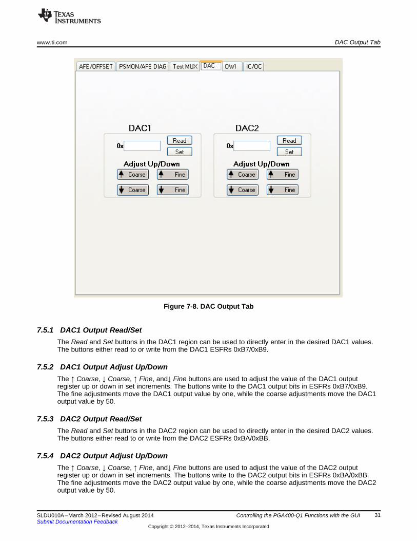
7.5 DAC Output TabThe DAC Output tab can be used to directly control the output of the VOUT1 and VOUT2 DACs on thePGA400-Q1. Figure 7-8 shows the DAC Output tab. The following sections describe the buttons on thistab.
30 Controlling the PGA400-Q1 Functions with the GUI SLDU010A–March 2012–Revised August 2014Submit Documentation Feedback
Copyright © 2012–2014, Texas Instruments Incorporated
www.ti.com DAC Output Tab
Figure 7-8. DAC Output Tab
7.5.1 DAC1 Output Read/SetThe Read and Set buttons in the DAC1 region can be used to directly enter in the desired DAC1 values.The buttons either read to or write from the DAC1 ESFRs 0xB7/0xB9.
7.5.2 DAC1 Output Adjust Up/DownThe ↑ Coarse, ↓ Coarse, ↑ Fine, and↓ Fine buttons are used to adjust the value of the DAC1 outputregister up or down in set increments. The buttons write to the DAC1 output bits in ESFRs 0xB7/0xB9.The fine adjustments move the DAC1 output value by one, while the coarse adjustments move the DAC1output value by 50.
7.5.3 DAC2 Output Read/SetThe Read and Set buttons in the DAC2 region can be used to directly enter in the desired DAC2 values.The buttons either read to or write from the DAC2 ESFRs 0xBA/0xBB.
7.5.4 DAC2 Output Adjust Up/DownThe ↑ Coarse, ↓ Coarse, ↑ Fine, and↓ Fine buttons are used to adjust the value of the DAC2 outputregister up or down in set increments. The buttons write to the DAC2 output bits in ESFRs 0xBA/0xBB.The fine adjustments move the DAC2 output value by one, while the coarse adjustments move the DAC2output value by 50.
31SLDU010A–March 2012–Revised August 2014 Controlling the PGA400-Q1 Functions with the GUISubmit Documentation Feedback
Copyright © 2012–2014, Texas Instruments Incorporated
OWI Tab www.ti.com
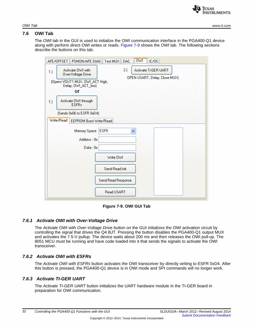
7.6 OWI TabThe OWI tab in the GUI is used to initialize the OWI communication interface in the PGA400-Q1 devicealong with perform direct OWI writes or reads. Figure 7-9 shows the OWI tab. The following sectionsdescribe the buttons on this tab.
Figure 7-9. OWI GUI Tab
7.6.1 Activate OWI with Over-Voltage DriveThe Activate OWI with Over-Voltage Drive button on the GUI initializes the OWI activation circuit bycontrolling the signal that drives the Q4 BJT. Pressing the button disables the PGA400-Q1 output MUXand activates the 7.5-V pullup. The device waits about 200 ms and then releases the OWI pull-up. The8051 MCU must be running and have code loaded into it that sends the signals to activate the OWItransceiver.
7.6.2 Activate OWI with ESFRsThe Activate OWI with ESFRs button activates the OWI transceiver by directly writing to ESFR 0xD4. Afterthis button is pressed, the PGA400-Q1 device is in OWI mode and SPI commands will no longer work.
7.6.3 Activate TI-GER UARTThe Activate TI-GER UART button initializes the UART hardware module in the TI-GER board inpreparation for OWI communication.
32 Controlling the PGA400-Q1 Functions with the GUI SLDU010A–March 2012–Revised August 2014Submit Documentation Feedback
Copyright © 2012–2014, Texas Instruments Incorporated

www.ti.com OWI Tab
7.6.4 Send SyncThe Send Sync button sends the required preliminary sync pulse to flush the contents of the OWItransceiver shift buffer.
7.6.5 Write/Read TabThe bottom portion of the main OWI tab is divided between performing simple OWI writes and reads andperforming OWI burst writes and reads. Figure 7-9 shows the Write/Read tab. The following sectionsdescribe the buttons on this tab.
7.6.5.1 Memory Space Selection BoxThe currently selected memory space in the Memory Space selection box is used to form the correctpacket when an OWI write or read is performed using the Write/Read buttons on the Write/Read tab.
7.6.5.2 Address Text BoxThe Address text box is used to enter the address that the user desires to write or read from when usingthe write and read buttons.
7.6.5.3 Data Text BoxThe Data text box is used to enter the data that the user desires to write or read from when using the writeand read buttons.
7.6.5.4 Write OWIThe Write OWI button collects information from the Memory Space selection box, the Address text box,and the Data text box and then form the appropriate packet to write the data into the selected address inthe correct memory space.
7.6.5.5 Send Read InitThe Send Read Init button collects information from the Memory Space selection box and the Addressand then form the appropriate packet to send in the Read Init command when reading from a selectedaddress in the correct memory space.
7.6.5.6 Send Read ResponseThe Send Read Response button sends the Read Response command to the PGA400-Q1 device that isbe followed by the data that was requested in the Read Init command.
7.6.5.7 Read USARTThe Read USART button reads out the contents of the TI-GER USART buffer. Data is shifted out of theFIFO buffer when the button is pressed and then displayed in the text box on the right side of theWrite/Read tab. Because the OWI always works in loop-back mode, the results of any OWI writes can beseen by reading the USART after a write is performed.
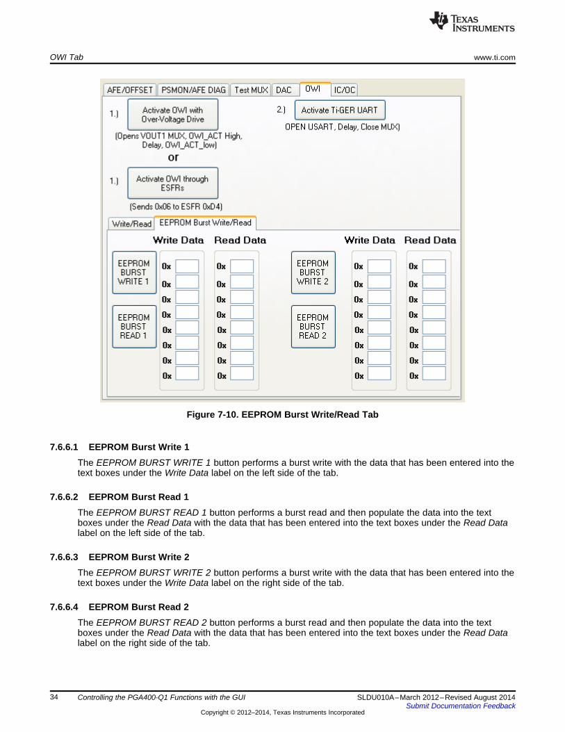
7.6.6 EEPROM Burst Write/Read TabThe second tab on the bottom portion of the OWI tab is the EEPROM Burst Write/Read tab. This tab isused to perform the EEPROM burst write and read commands that the PGA400-Q1 device supports.Figure 7-10 shows the EEPROM Burst Write/Read tab. The following sections describe the buttons on thistab.
33SLDU010A–March 2012–Revised August 2014 Controlling the PGA400-Q1 Functions with the GUISubmit Documentation Feedback
Copyright © 2012–2014, Texas Instruments Incorporated
OWI Tab www.ti.com
Figure 7-10. EEPROM Burst Write/Read Tab
7.6.6.1 EEPROM Burst Write 1The EEPROM BURST WRITE 1 button performs a burst write with the data that has been entered into thetext boxes under the Write Data label on the left side of the tab.
7.6.6.2 EEPROM Burst Read 1The EEPROM BURST READ 1 button performs a burst read and then populate the data into the textboxes under the Read Data with the data that has been entered into the text boxes under the Read Datalabel on the left side of the tab.
7.6.6.3 EEPROM Burst Write 2The EEPROM BURST WRITE 2 button performs a burst write with the data that has been entered into thetext boxes under the Write Data label on the right side of the tab.
7.6.6.4 EEPROM Burst Read 2The EEPROM BURST READ 2 button performs a burst read and then populate the data into the textboxes under the Read Data with the data that has been entered into the text boxes under the Read Datalabel on the right side of the tab.
34 Controlling the PGA400-Q1 Functions with the GUI SLDU010A–March 2012–Revised August 2014Submit Documentation Feedback
Copyright © 2012–2014, Texas Instruments Incorporated
www.ti.com IC/OC Tab
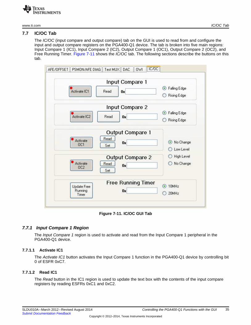
7.7 IC/OC TabThe IC/OC (input compare and output compare) tab on the GUI is used to read from and configure theinput and output compare registers on the PGA400-Q1 device. The tab is broken into five main regions:Input Compare 1 (IC1), Input Compare 2 (IC2), Output Compare 1 (OC1), Output Compare 2 (OC2), andFree Running Timer. Figure 7-11 shows the IC/OC tab. The following sections describe the buttons on thistab.
Figure 7-11. IC/OC GUI Tab
7.7.1 Input Compare 1 RegionThe Input Compare 1 region is used to activate and read from the Input Compare 1 peripheral in thePGA400-Q1 device.
7.7.1.1 Activate IC1The Activate IC1 button activates the Input Compare 1 function in the PGA400-Q1 device by controlling bit0 of ESFR 0xC7.
7.7.1.2 Read IC1The Read button in the IC1 region is used to update the text box with the contents of the input compareregisters by reading ESFRs 0xC1 and 0xC2.
35SLDU010A–March 2012–Revised August 2014 Controlling the PGA400-Q1 Functions with the GUISubmit Documentation Feedback
Copyright © 2012–2014, Texas Instruments Incorporated
IC/OC Tab www.ti.com
7.7.1.3 Falling/Rising Edge Selection BoxThe Falling/Rising Edge selection box is used to change the polarity that the input compare peripheraluses by controlling bit 1 of ESFR 0xC0.
7.7.2 Input Compare 2 RegionThe Input Compare 2 region is used to activate and read from the Input Compare 2 peripheral in thePGA400-Q1.
7.7.2.1 Activate IC2The Activate IC2 button activates the Input Compare 2 function in the PGA400-Q1 device by controlling bit1 of ESFR 0xC7.
7.7.2.2 Read IC2The Read button in the IC2 region is used to update the text box with the contents of the input compareregisters by reading ESFRs 0xC3 and 0xC4.
7.7.2.3 Falling/Rising Edge Selection BoxThe Falling/Rising Edge selection box is used to change the polarity that the input compare peripheraluses by controlling bit 2 of ESFR 0xC0.
7.7.3 Output Compare 1 RegionThe Output Compare 1 region is used to activate and set/read the Output Compare 1 peripheral in thePGA400-Q1.
7.7.3.1 Activate OC1The Activate OC1 button activates the Output Compare 1 function in the PGA400-Q1 device by controllingbit 2 of ESFR 0xC7.
7.7.3.2 Read OC1The Read button in the OC1 region is used to update the text box with the contents of the output compareregisters by reading ESFRs 0xC5 and 0xC6.
7.7.3.3 Set OC1The Set button in the OC1 region is used to set the value in the Output Compare 1 register by writing toESFR 0xC5 and 0xC6.
7.7.4 Output Compare 2 RegionThe Output Compare 2 region is used to activate and set and read the Output Compare 2 peripheral in thePGA400-Q1.
7.7.4.1 Activate OC2The Activate OC2 button activates the Output Compare 2 function in the PGA400-Q1 device by controllingbit 3 of ESFR 0xC7.
7.7.4.2 Read OC2The Read button in the OC2 region is used to update the text box with the contents of the output compareregisters by reading ESFRs 0xC9 and 0xCA.
36 Controlling the PGA400-Q1 Functions with the GUI SLDU010A–March 2012–Revised August 2014Submit Documentation Feedback
Copyright © 2012–2014, Texas Instruments Incorporated

www.ti.com IC/OC Tab
7.7.4.3 Set OC2The Set button in the OC2 region is used to set the value in the Output Compare 2 register by writing toESFR 0xC9 and 0xCA.
7.7.5 No Change / Low Level / High Level Selection BoxThe No Change / Low Level / High Level selection box is used to control the level that both the OC1 andOC2 peripherals use for the output compare functions. This control is achieved by controlling bits 3 and 4of ESFR 0xC0.
7.7.6 Free Running Timer RegionThe Free Running Timer region of the IC/OC tab is used to monitor the Free Running Timer in thePGA400-Q1.
7.7.6.1 Update Free Running TimerThe Update Free Running Timer button is used to populate the text box in the Free Running Timer regionwith the contents of the PGA400-Q1 Free Running Timer.
7.7.6.2 10MHz / 20MHz Selection BoxThe 10MHz / 20MHz selection box is used to select between a 10-MHz and 20-MHz Free Running Timerinside the PGA400-Q1 device by controlling bit 0 of ESFR 0xC0.
37SLDU010A–March 2012–Revised August 2014 Controlling the PGA400-Q1 Functions with the GUISubmit Documentation Feedback
Copyright © 2012–2014, Texas Instruments Incorporated
12
C4
0.1uF,16V,X7R
12
C3
0.1uF,16V,X7R
12
C5
0.1uF,16V,X7R
12
C2
0.1uF,16V,X7R
VP_OTP
GND
GND
GND
/CSSCKMOSIMISO
VBRG
VDD
GND
1234
H1
Header 4
GND
VIN1PVIN1N
VIN2PVIN2N
VIN3
TIPTIN
ICAP1ICAP2
RxDTxD
VOUT1
VOUT2
CS_MB
SCLK_MBMOSI_MBMISO_MB
GPIO_1GPIO_2GPIO_3GPIO_4GPIO_5GPIO_6
VBRGICAP1ICAP2
VIN1PVIN1N
VIN2PVIN2N
VIN3
TIPTIN
AVDDDVDD
AVDDDVDD
VDDVDD VP_OTP
VP_OTP
/CSSCKMOSIMISO
VOUT2
VOUT1
GPIO1GPIO2GPIO3GPIO4
GPIO5
GPIO6
RXDTXD
GND
GND
123456
H2
Header 6
GPIO_1GPIO_2GPIO_3GPIO_4
C636pF,50V,C0G
C736pF,50V,C0G
GND
R40.0R
GPIO_5 GPIO_6
R51M
2 4
X1 ECS-400-20-30B-DU40MHz - 20pF Load
R30.0R
R1
0.0RR2
0.0RGPIO_5*GPIO_6*
JP1
DVDD
AVDD
12
C1
1uF,16V,X7R
V7P5_MB+7.5V
JP2
VDD_MB
R8D
R8C
R8B
R8A47k
GND
GPIO_2
GPIO_4
GPIO_5*
GPIO_6*
DNI DNI
To use XTAL, remove R1 & R2 and install a 0 Ohm resistor or short R3 & R4
PGA400-Q1 - Main
R930510,0805,1/8W,5%D30
LED2
GND
R9311.1kD31
LED2
GND
VBRG9
VIN1P10
VIN1N12
VIN2P13
VIN2N15
ICAP111
ICAP214
TIP7
TIN8
GN
D5
AV
SS
19
VIN316
VOUT1/DIO4
NC
30
NC
23
NC
17
AVDD20
VDD21
VOUT26
VP_OTP3
SPI_MOSI28
DVDD24
GPIO_1/IIC_SDA2
GPIO_21
SPI_SCK29
SPI_CSN26
SPI_MISO27
DV
SS
22
GPIO_3/IIC_SCL36
GPIO_5/XTAL134
GPIO_6/XTAL233
GPIO_435
RxD32
TxD31
RE
F_G
ND
18
GN
D25
PW
RP
AD
0
U1PGA400 -Q1- QFN
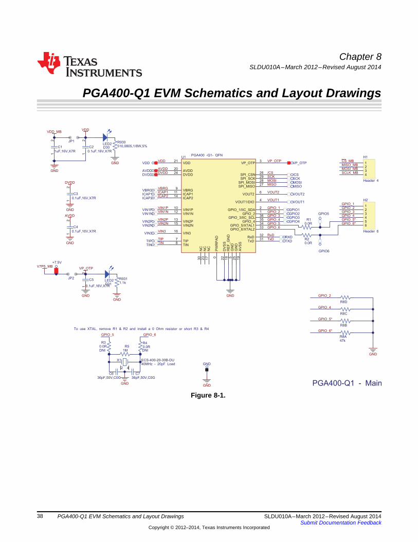
Chapter 8SLDU010A–March 2012–Revised August 2014
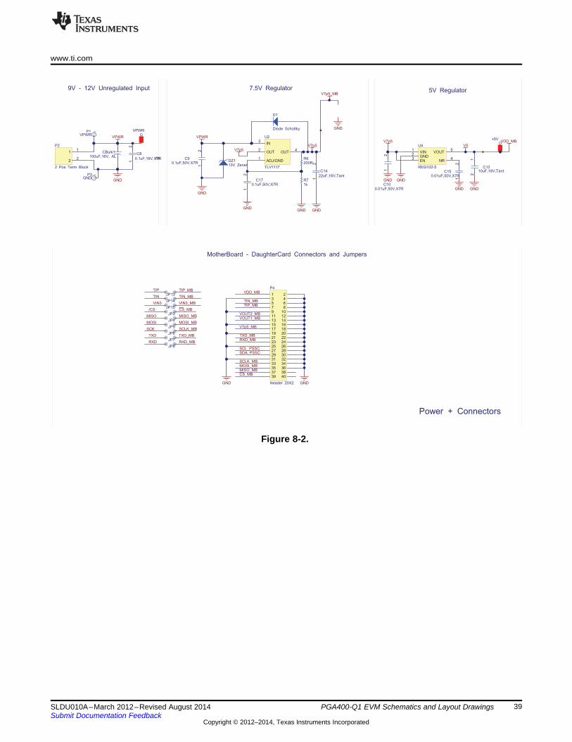
PGA400-Q1 EVM Schematics and Layout Drawings
Figure 8-1.
38 PGA400-Q1 EVM Schematics and Layout Drawings SLDU010A–March 2012–Revised August 2014Submit Documentation Feedback
Copyright © 2012–2014, Texas Instruments Incorporated
12
C8
0.1uF,16V,X7R
FP1VPWR
VPWR
CBulk1100uF,16V, AL
GNDFP3
GND
RXDJP7
JP8RXD_MB
TXD TXD_MB
VOUT2_MBVOUT1_MB
TIP_MBTIN_MB
VDD_MB
11
22
P2
2 Pos Term Block
CS_MBMISO_MBMOSI_MBSCLK_MB
SDA_PSSCSCL_PSSC
RXD_MBTXD_MB
GNDGND
+5V
VPWR
/CS
SCK
MOSI
MISOJP3
JP4
JP5
JP6
CS_MB
MISO_MB
MOSI_MB
SCLK_MB
JP13
JP14
TIP
TIN
TIP_MB
TIN_MB
JP15VIN3 VIN3_MB
GNDGND
12
C90.1uF,50V,X7R
12
C170.1uF,50V,X7R
GND
R6200R
R71k
GND
12
C14
22uF,16V,Tant
GND
D1
Diode Schottky
VDD_MBVPWR
V7p5_MB
VIN1
GND2
EN3
NR4
VOUT5
U4
REG102-5
GND 12
C150.01uF,50V,X7R
V5
12
C100.01uF,50V,X7R
12
C1210uF,16V,Tant
GND
GND
V7p5
DZ113V Zener
9V - 12V Unregulated Input
GND
V7p5
7.5V Regulator 5V Regulator
7R
MotherBoard - DaughterCard Connectors and Jumpers
V7p5
Power + Connectors
IN3
OUT2
ADJ/GND1
OUT4
U2
TLV1117
1 23 45 67 89 1011 1213 1415 1617 1819 2021 2223 2425 2627 2829 3031 3233 3435 3637 3839 40
P4
Header 20X2
V7p5_MB
www.ti.com
Figure 8-2.
39SLDU010A–March 2012–Revised August 2014 PGA400-Q1 EVM Schematics and Layout DrawingsSubmit Documentation Feedback
Copyright © 2012–2014, Texas Instruments Incorporated
C1930pF
C2056pF
C2230pF
C2356pF
ICAP1
ICAP2
VIN2P_C
VIN2N_C
VIN1P_C
VIN1N_C
7.0-50pFC18
Cap Var
7.0-50pFC21
Cap Var
JP17
JP19
JP10
JP12
VIN2P_C
VIN2N_C
VIN1P_C
VIN1N_C
VIN2P_R
VIN2N_R
VIN1P_R
VIN1N_R
VIN1P
VIN1N
VIN2P
VIN2N
12
C260.01uF
12
C310.01uF
12
C321nF
12
C281nF
12
C241nF
GND
GND
GND
12
C271nF
GND
JP16
JP18
JP11
JP9
VIN1P_MB
VIN1N_MB
VIN2P_MB
VIN2N_MB
C2510nF - X2Y
C2910nF - X2Y
GND GND
GND GND
VOUTA1
VOUTB2
VREFH3
VD
D4
VREFL5
GN
D6
VOUTC7
VOUTD8
LDAC9
SCL10
SDA11
IOV
DD
12
A013
A114
A215
A416
U8DAC8574
GND
V5
12
C360.1uF,16V,X7R
GND
GND
DAC1_1DAC1_2DAC1_3DAC1_4
2
31
A
84
U5AOPA2335UA
GND
V5
R241k
5
67
B
84
U5BOPA2335UA
R251k
12
C351uF,16V,X7R
GND
V5
GND
GND
V5
R32
1k
R311k
GND
GND
V5
R361k R35
1k
12
C421uF,16V,X7R
GND
V5
GND
GND
V5
R401k R41
1k
GND
DAC1_1
DAC1_2
DAC1_3
DAC1_4
DAC1_1_BUF
DAC1_2_BUF
DAC1_3_BUF
DAC1_4_BUF
MB_SDAMB_SCL
1 2
C302.2nF,16V,X7R
1 2
C382.2nF,16V,X7R
1 2
C412.2nF,16V,X7R
1 2
C332.2nF,16V,X7R
V5
5
67
B
84
U10BOPA2335UA
2
31
A
84
U10AOPA2335UA
4 Channel DAC and DAC Buffers
GND
V5
1 2
C340.1uF,16V,X7R
GND
V5
1 2
C370.1uF,16V,X7R
GND
V5
1 2
C390.1uF,16V,X7R
GND
V5
1 2
C400.1uF,16V,X7R
NO11
NO22
NO33
COM7
GND4
IN25
IN16
VCC8
U6
TS5A3359
GND
GND
GND
GND
DAC1_1_BUF
DAC1_2_BUF
DAC1_3_BUF
DAC1_4_BUF
TIP_MB
TIN_MB
VIN3_MB
R3349.9k
R3449.9k
R3749.9k
R4349.9k
GND
GND
GND
GND
R4249.9k
GND
VIN1P_MB*
VIN1N_MB*
VIN2P_MB*
VIN2N_MB*
3PST_13PST_2
3PST_13PST_2
3PST_13PST_2
3PST_13PST_2
R39 49.9k
R38 49.9k
NO11
NO22
NO33
COM7
GND4
IN25
IN16
VCC8
U7
TS5A3359
NO11
NO22
NO33
COM7
GND4
IN25
IN16
VCC8
U9
TS5A3359
NO11
NO22
NO33
COM7
GND4
IN25
IN16
VCC8
U11
TS5A3359
4 x 3PST MUX for Buffer Outputs
R910k
R1010k
R177.5k
R187.5k
GND
R1910k
R2010k
R297.5k
R307.5k
GND
VBRG
VBRG
VIN1P_MB VIN1N_MB
VIN2P_MB VIN2N_MB
5kR15 RPot
5kR28 RPot
5kR14RPot
5kR27RPot
Resistive Bridge
VIN1P_MB*R12
0.0R
VIN1N_MB*R13
0.0R
VIN2P_MB*R22
0.0R
VIN2N_MB*R23
0.0R
Cap Sensor
Input Filtering and Input Selection
V5
DACs / Inputs
L1
51R
L2
51R
L3
51R
L4
51R
51- Resistors are Installed Instead of Ferrite BeadΩ s: L1 - L4. Remove the 51-Ω resistors and replace with Ferrites if desired.
DNI
DNI
www.ti.com
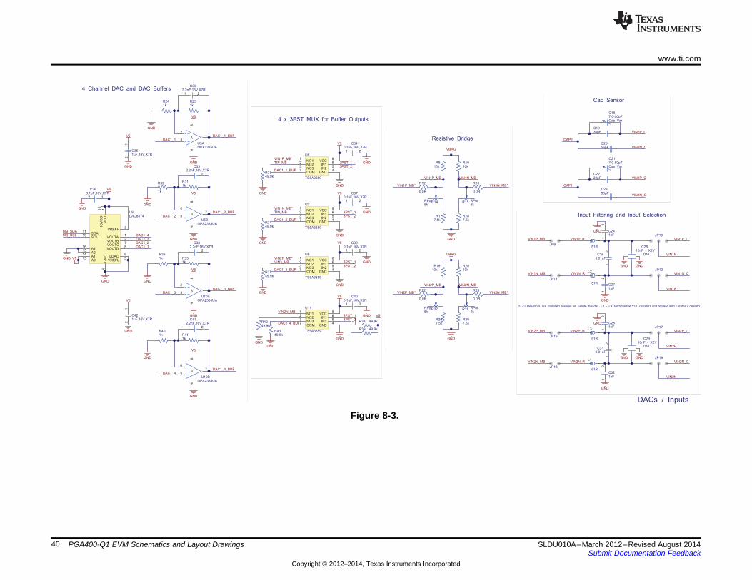
Figure 8-3.
40 PGA400-Q1 EVM Schematics and Layout Drawings SLDU010A–March 2012–Revised August 2014Submit Documentation Feedback
Copyright © 2012–2014, Texas Instruments Incorporated
R55
4.99k
R534.99k
V5
12
C540.1uF,50V,X7R
GND
2
31
A
84
U19AOPA2335UA
GND
V5
GND
12
C531uF,16V,X7R
R54200R
1 2
C50100pF,250V,C0G
V2.5
5
67
B
84
U19BOPA2335UA
R5149.9k
V5
GND
1 2
C480.1uF,16V,X7R
GND
ADC3
ADC4
DAC1_3_BUF
DAC1_4_BUF
12
C521uF,16V,X7R
GND
V5
DAC1_1_BUF
DAC1_2_BUFSPDT_1SPDT_1
R5249.9k
GND
NC19
COM110
NO12
V+8
GND3
NC27
COM26
NO24
IN25
IN11
U17
TS5A23159
+2.5V
12
C47
100pF,50V,,X7R
12
C44
100pF,50V,,X7R
GND
GND
VOUT1
VOUT2
4
NC
13
5
2
U12SN74LVC1G07
GND
V5
R4449k
4
NC
13
5
2
U13SN74LVC1G07
R4549k
V5
GND
R46200R
R47
49k
R48
49k
V5
V5TX
RX
OWI_TX_RX
GND
GND
GND
GND
GND
V5
V5
V5
V5
1 2
C430.1uF,50V,X7R
GND
1 2
C450.1uF,50V,X7R
GND
1 2
C490.1uF,50V,X7R
GND
1 2
C510.1uF,50V,X7R
V2.5
NO11
COM12
NO23
VDD14
NO411
GND7
COM24
COM39
NO38
COM410
IN412
IN36
IN25
IN113
U15
TS12A44514
GND
1 2C46
0.1uF,16V,X7R
GND
ADC1
ADC2
ADC3
ADC4
V2.5
V2.5
V2.5
COM4
VOUT2_MB
NO4
ADC1
ADC2
OWI_TX_RX
4SPST_14SPST_14SPST_24SPST_2
JP23
JP22
VOUT1_MB
VOUT2_MB
VOUT1_MB
VOUT1_MB
MB_SDA
MB_SCL
MB_SDA
MB_SCL
MB_SDA
MB_SCL
MB_SDA
MB_SCL
R4949.9k
R5049.9k
GND GND
VIN+1
GN
D2
SCL3
SDA4
VD
D5
VIN-6
U14
ADS1100A2
VIN+1
GN
D2
SCL3
SDA4
VD
D5
VIN-6
U20
ADS1100A5
VIN+1
GN
D2
SCL3
SDA4
VD
D5
VIN-6
U16
ADS1100A3
VIN+1
GN
D2
SCL3
SDA4
VD
D5
VIN-6
U18
ADS1100A4
4 x ADCOWI -> TX/RX
2.5V Reference for ADCs
PSSC DAC Output MUX
ADC3 & ADC4 Input MUX
PSSC DAC Outputs
Outputs / Acquisition
V7p5_MB
TX
RX
OWI
www.ti.com
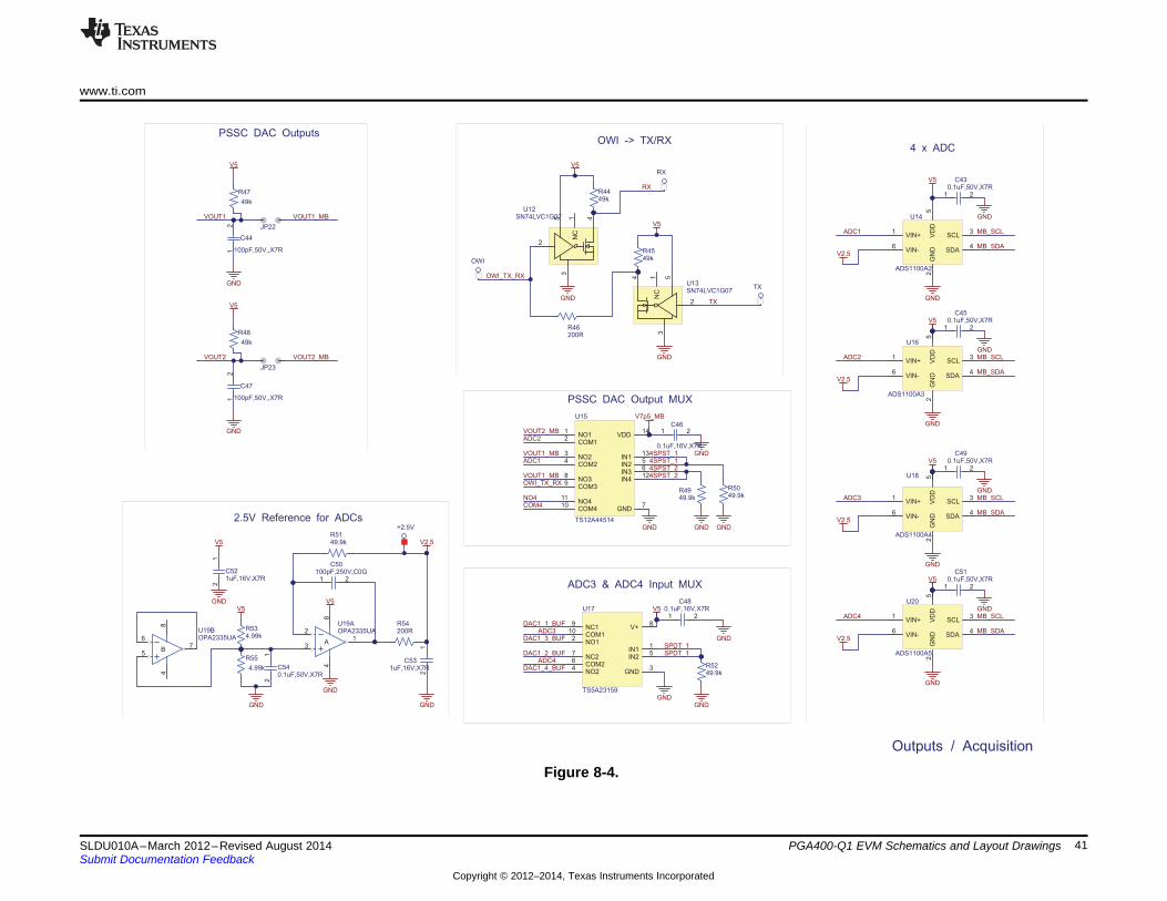
Figure 8-4.
41SLDU010A–March 2012–Revised August 2014 PGA400-Q1 EVM Schematics and Layout DrawingsSubmit Documentation Feedback
Copyright © 2012–2014, Texas Instruments Incorporated
C620.1uF,50V,X7R
C630.1uF,50V,X7R
C600.1uF,50V,X7R
C610.1uF,50V,X7R
C64
0.1uF,50V,X7R
CPU_TX
CPU_RX
1
2
3
4
5
6
7
8
9
11
10
J1
Female
CPU_TX
CPU_RX
CPU_RX
CPU_TX
GND
GND
GND
GND
GND
V5
C1+2
C1-4
C2+5
C2-6
T1IN11
R1OUT9
EN1
FORCEON12
GND14
V+3
V-7
T1OUT13
R1IN8
VCC15
FORCEOFF16
~INVALID10
232 TX
TTL TX
TTL RX
232 RX
U23
MAX3221ECAE
R70
10R
RXD_MB
TXD_MB
JP26
JP27
PSSC RXD/TXD -> RS-232
Communications
Q3SI2319DS-T1-E3
R66
220k
R685R
R641k
GND
12
C59330nF,16V,X7R
GND
R6949.9k
GNDVOUT1_MB
V7p5_MB
Q42N2222
OWI_ACT
OWI_T
DZ45.1V Zener
OWI_Activation
DNI
www.ti.com
Figure 8-5.
Figure 8-6.
42 PGA400-Q1 EVM Schematics and Layout Drawings SLDU010A–March 2012–Revised August 2014Submit Documentation Feedback
Copyright © 2012–2014, Texas Instruments Incorporated
MISO, SDA1
SCLK, SCL3
CS (SS)5
MOSI7
IO-119
IO-011
IO-213
IO-415
IO-617
V_5.0V (OUT)19
CHIP OSC (OUT)21
V_3.3V (OUT)23
GND2
IO-10 (PIC OSC)24
PWR-DWN22
IO-9, RX20
IO-718
IO-516
IO-314
IO-112
IO-8, TX10
GND8
GND6
GND4
TIGER - A
DVM-125
DVM-227
DVM-329
IO-DAC30
IO-B28
IO-A26
TIGER - A
R75D
R75C
IO-0IO-2IO-4
IO-CSIO-SCLK
IO-MOSI
IO-MISO
IO-11
IO-6V_5.0_WORLD
V_3.3_WORLDV_DVM_1V_DVM_2V_DVM_3
GNDGND
GNDGND
IO-1IO-3IO-5
IO-10 (SLOW OSC)
IO-8__TX
IO-9__RXPWR-DWN
IO-7
IO-AIO-BDAC_OUT
IO-CS
IO-SCLK
IO-MOSI
IO-MISO
R75B
R81D
R75A100,0805,1/10W,5%
R81C
R81B
R87D
R81A100,0805,1/10W,5%
R87C
IO-0
IO-2
IO-4
IO-6
IO-1
OWI_T
IO-5
R87B
R94D
R87A100,0805,1/10W,5%
R94C
IO-7
IO-10 (SLOW OSC)
IO-11
V_5.0_WORLD
IO-OSC
R94B
R94A100,0805,1/10W,5%
CS_T
SCLK_T
MISO_T
MOSI_T
V_3.3_WORLD
R93510,0805,1/8W,5%D3
LED2
GND
R88332, 0805,1/8W,5%D2
LED2
GND
GND GND GND GNDGND GND GND GND GND
Digital Pins / TI - GER
NC19
COM110
NO12
V+8
GND3
NC27
COM26
NO24
IN25
IN11
U27
TS5A23159
V51 2
C690.1uF.16V,X7R
GND
GND
SCLK_T
MOSI_TMISO_TSDA
SCLK_MBR7649.9k
GND
4B114
S1
1B12
4B213
1B23
1A4
3A9
2B26
2B15
4A12
GND8
2A7
3B111
VCC16
3B210
OE15
U26
SN74CBTLV3257
V51 2
C680.1uF.16V,X7R
GND
SPI/I2C
CS_TMISO_MBMOSI_MB
CS_MBSCL
GND
R7849.9k
GNDR79
49.9k
GND
SDA
SCL
SDA_PSSC
SCL_PSSCI2C_MB/PSSC
IO-8__TX
SPI/I2C
I2C_MB/PSSC
TX
IO-3 4SPST_1
4SPST_2
3PST_1
3PST_2
IO-9__RX
SPDT_1
RX
R7749.9k
COMM_EN
COMM_EN
SDA_PSSC
SCL_PSSC
JP29
JP28
GPIO_3
GPIO_1
GND GND GND GND GND GND GND GND GND
R91
49.9k
R8949.9k
GND GNDGND
GND GND GND
GND GNDGND
GND GND GND
GND
R8049.9k
GND
TI BUG
MISO_TSCLK_T/CS_TMOSI_T
OWI_T
SPDT_13PST_2
I2C_MB/PSSC
SPI/I2C TX
RXV3intD
4SPST_14SPST_23PST_1COMM_EN
TI-GER COMM MUX - SPI/I2C
I2C MUX - PSSC / EVM
V5
MB_SDA
MB_SCL
OE1
A2
GND3
VCC5
Y4
U25
SN74LVC1G240
V5
GND
4SPST_1
4PST_EN
4PST_EN
www.ti.com
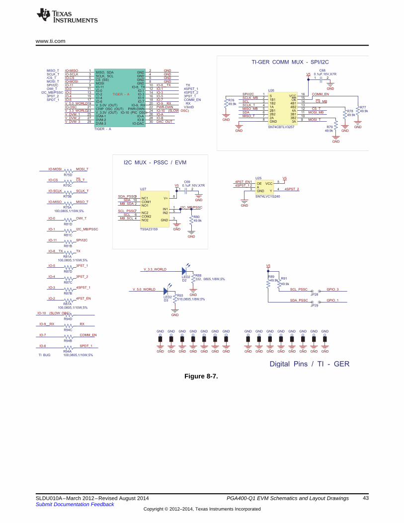
Figure 8-7.
43SLDU010A–March 2012–Revised August 2014 PGA400-Q1 EVM Schematics and Layout DrawingsSubmit Documentation Feedback
Copyright © 2012–2014, Texas Instruments Incorporated
www.ti.com
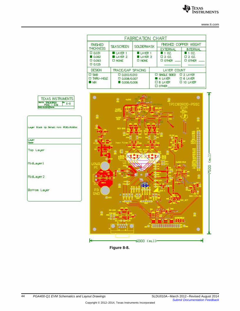
Figure 8-8.
44 PGA400-Q1 EVM Schematics and Layout Drawings SLDU010A–March 2012–Revised August 2014Submit Documentation Feedback
Copyright © 2012–2014, Texas Instruments Incorporated

www.ti.com Revision History
Revision History
Changes from Original (March 2012) to A Revision ....................................................................................................... Page
• Deleted Reference to the Chapter 8: Controlling the EVM peripherals with the GUI section ................................... 1
NOTE: Page numbers for previous revisions may differ from page numbers in the current version.
45SLDU010A–March 2012–Revised August 2014 Revision HistorySubmit Documentation Feedback
Copyright © 2012–2014, Texas Instruments Incorporated

ADDITIONAL TERMS AND CONDITIONS, WARNINGS, RESTRICTIONS, AND DISCLAIMERS FOREVALUATION MODULES
Texas Instruments Incorporated (TI) markets, sells, and loans all evaluation boards, kits, and/or modules (EVMs) pursuant to, and userexpressly acknowledges, represents, and agrees, and takes sole responsibility and risk with respect to, the following:
1. User agrees and acknowledges that EVMs are intended to be handled and used for feasibility evaluation only in laboratory and/ordevelopment environments. Notwithstanding the foregoing, in certain instances, TI makes certain EVMs available to users that do nothandle and use EVMs solely for feasibility evaluation only in laboratory and/or development environments, but may use EVMs in ahobbyist environment. All EVMs made available to hobbyist users are FCC certified, as applicable. Hobbyist users acknowledge, agree,and shall comply with all applicable terms, conditions, warnings, and restrictions in this document and are subject to the disclaimer andindemnity provisions included in this document.
2. Unless otherwise indicated, EVMs are not finished products and not intended for consumer use. EVMs are intended solely for use bytechnically qualified electronics experts who are familiar with the dangers and application risks associated with handling electricalmechanical components, systems, and subsystems.
3. User agrees that EVMs shall not be used as, or incorporated into, all or any part of a finished product.4. User agrees and acknowledges that certain EVMs may not be designed or manufactured by TI.5. User must read the user's guide and all other documentation accompanying EVMs, including without limitation any warning or
restriction notices, prior to handling and/or using EVMs. Such notices contain important safety information related to, for example,temperatures and voltages. For additional information on TI's environmental and/or safety programs, please visit www.ti.com/esh orcontact TI.
6. User assumes all responsibility, obligation, and any corresponding liability for proper and safe handling and use of EVMs.7. Should any EVM not meet the specifications indicated in the user’s guide or other documentation accompanying such EVM, the EVM
may be returned to TI within 30 days from the date of delivery for a full refund. THE FOREGOING LIMITED WARRANTY IS THEEXCLUSIVE WARRANTY MADE BY TI TO USER AND IS IN LIEU OF ALL OTHER WARRANTIES, EXPRESSED, IMPLIED, ORSTATUTORY, INCLUDING ANY WARRANTY OF MERCHANTABILITY OR FITNESS FOR ANY PARTICULAR PURPOSE. TI SHALLNOT BE LIABLE TO USER FOR ANY INDIRECT, SPECIAL, INCIDENTAL, OR CONSEQUENTIAL DAMAGES RELATED TO THEHANDLING OR USE OF ANY EVM.
8. No license is granted under any patent right or other intellectual property right of TI covering or relating to any machine, process, orcombination in which EVMs might be or are used. TI currently deals with a variety of customers, and therefore TI’s arrangement withthe user is not exclusive. TI assumes no liability for applications assistance, customer product design, software performance, orinfringement of patents or services with respect to the handling or use of EVMs.
9. User assumes sole responsibility to determine whether EVMs may be subject to any applicable federal, state, or local laws andregulatory requirements (including but not limited to U.S. Food and Drug Administration regulations, if applicable) related to its handlingand use of EVMs and, if applicable, compliance in all respects with such laws and regulations.
10. User has sole responsibility to ensure the safety of any activities to be conducted by it and its employees, affiliates, contractors ordesignees, with respect to handling and using EVMs. Further, user is responsible to ensure that any interfaces (electronic and/ormechanical) between EVMs and any human body are designed with suitable isolation and means to safely limit accessible leakagecurrents to minimize the risk of electrical shock hazard.
11. User shall employ reasonable safeguards to ensure that user’s use of EVMs will not result in any property damage, injury or death,even if EVMs should fail to perform as described or expected.
12. User shall be solely responsible for proper disposal and recycling of EVMs consistent with all applicable federal, state, and localrequirements.
Certain Instructions. User shall operate EVMs within TI’s recommended specifications and environmental considerations per the user’sguide, accompanying documentation, and any other applicable requirements. Exceeding the specified ratings (including but not limited toinput and output voltage, current, power, and environmental ranges) for EVMs may cause property damage, personal injury or death. Ifthere are questions concerning these ratings, user should contact a TI field representative prior to connecting interface electronics includinginput power and intended loads. Any loads applied outside of the specified output range may result in unintended and/or inaccurateoperation and/or possible permanent damage to the EVM and/or interface electronics. Please consult the applicable EVM user's guide priorto connecting any load to the EVM output. If there is uncertainty as to the load specification, please contact a TI field representative. Duringnormal operation, some circuit components may have case temperatures greater than 60°C as long as the input and output are maintainedat a normal ambient operating temperature. These components include but are not limited to linear regulators, switching transistors, passtransistors, and current sense resistors which can be identified using EVMs’ schematics located in the applicable EVM user's guide. Whenplacing measurement probes near EVMs during normal operation, please be aware that EVMs may become very warm. As with allelectronic evaluation tools, only qualified personnel knowledgeable in electronic measurement and diagnostics normally found indevelopment environments should use EVMs.Agreement to Defend, Indemnify and Hold Harmless. User agrees to defend, indemnify, and hold TI, its directors, officers, employees,agents, representatives, affiliates, licensors and their representatives harmless from and against any and all claims, damages, losses,expenses, costs and liabilities (collectively, "Claims") arising out of, or in connection with, any handling and/or use of EVMs. User’sindemnity shall apply whether Claims arise under law of tort or contract or any other legal theory, and even if EVMs fail to perform asdescribed or expected.Safety-Critical or Life-Critical Applications. If user intends to use EVMs in evaluations of safety critical applications (such as life support),and a failure of a TI product considered for purchase by user for use in user’s product would reasonably be expected to cause severepersonal injury or death such as devices which are classified as FDA Class III or similar classification, then user must specifically notify TIof such intent and enter into a separate Assurance and Indemnity Agreement.

RADIO FREQUENCY REGULATORY COMPLIANCE INFORMATION FOR EVALUATION MODULESTexas Instruments Incorporated (TI) evaluation boards, kits, and/or modules (EVMs) and/or accompanying hardware that is marketed, sold,or loaned to users may or may not be subject to radio frequency regulations in specific countries.General Statement for EVMs Not Including a RadioFor EVMs not including a radio and not subject to the U.S. Federal Communications Commission (FCC) or Industry Canada (IC)regulations, TI intends EVMs to be used only for engineering development, demonstration, or evaluation purposes. EVMs are not finishedproducts typically fit for general consumer use. EVMs may nonetheless generate, use, or radiate radio frequency energy, but have not beentested for compliance with the limits of computing devices pursuant to part 15 of FCC or the ICES-003 rules. Operation of such EVMs maycause interference with radio communications, in which case the user at his own expense will be required to take whatever measures maybe required to correct this interference.General Statement for EVMs including a radioUser Power/Frequency Use Obligations: For EVMs including a radio, the radio included in such EVMs is intended for development and/orprofessional use only in legally allocated frequency and power limits. Any use of radio frequencies and/or power availability in such EVMsand their development application(s) must comply with local laws governing radio spectrum allocation and power limits for such EVMs. It isthe user’s sole responsibility to only operate this radio in legally acceptable frequency space and within legally mandated power limitations.Any exceptions to this are strictly prohibited and unauthorized by TI unless user has obtained appropriate experimental and/or developmentlicenses from local regulatory authorities, which is the sole responsibility of the user, including its acceptable authorization.
U.S. Federal Communications Commission Compliance
For EVMs Annotated as FCC – FEDERAL COMMUNICATIONS COMMISSION Part 15 Compliant
CautionThis device complies with part 15 of the FCC Rules. Operation is subject to the following two conditions: (1) This device may not causeharmful interference, and (2) this device must accept any interference received, including interference that may cause undesired operation.Changes or modifications could void the user's authority to operate the equipment.
FCC Interference Statement for Class A EVM devicesThis equipment has been tested and found to comply with the limits for a Class A digital device, pursuant to part 15 of the FCC Rules.These limits are designed to provide reasonable protection against harmful interference when the equipment is operated in a commercialenvironment. This equipment generates, uses, and can radiate radio frequency energy and, if not installed and used in accordance with theinstruction manual, may cause harmful interference to radio communications. Operation of this equipment in a residential area is likely tocause harmful interference in which case the user will be required to correct the interference at its own expense.
FCC Interference Statement for Class B EVM devicesThis equipment has been tested and found to comply with the limits for a Class B digital device, pursuant to part 15 of the FCC Rules.These limits are designed to provide reasonable protection against harmful interference in a residential installation. This equipmentgenerates, uses and can radiate radio frequency energy and, if not installed and used in accordance with the instructions, may causeharmful interference to radio communications. However, there is no guarantee that interference will not occur in a particular installation. Ifthis equipment does cause harmful interference to radio or television reception, which can be determined by turning the equipment off andon, the user is encouraged to try to correct the interference by one or more of the following measures:
• Reorient or relocate the receiving antenna.• Increase the separation between the equipment and receiver.• Connect the equipment into an outlet on a circuit different from that to which the receiver is connected.• Consult the dealer or an experienced radio/TV technician for help.
Industry Canada Compliance (English)For EVMs Annotated as IC – INDUSTRY CANADA Compliant:
This Class A or B digital apparatus complies with Canadian ICES-003.Changes or modifications not expressly approved by the party responsible for compliance could void the user’s authority to operate theequipment.
Concerning EVMs Including Radio TransmittersThis device complies with Industry Canada licence-exempt RSS standard(s). Operation is subject to the following two conditions: (1) thisdevice may not cause interference, and (2) this device must accept any interference, including interference that may cause undesiredoperation of the device.
Concerning EVMs Including Detachable AntennasUnder Industry Canada regulations, this radio transmitter may only operate using an antenna of a type and maximum (or lesser) gainapproved for the transmitter by Industry Canada. To reduce potential radio interference to other users, the antenna type and its gain shouldbe so chosen that the equivalent isotropically radiated power (e.i.r.p.) is not more than that necessary for successful communication.This radio transmitter has been approved by Industry Canada to operate with the antenna types listed in the user guide with the maximumpermissible gain and required antenna impedance for each antenna type indicated. Antenna types not included in this list, having a gaingreater than the maximum gain indicated for that type, are strictly prohibited for use with this device.

Canada Industry Canada Compliance (French)
Cet appareil numérique de la classe A ou B est conforme à la norme NMB-003 du Canada
Les changements ou les modifications pas expressément approuvés par la partie responsable de la conformité ont pu vider l’autorité del'utilisateur pour actionner l'équipement.
Concernant les EVMs avec appareils radio
Le présent appareil est conforme aux CNR d'Industrie Canada applicables aux appareils radio exempts de licence. L'exploitation estautorisée aux deux conditions suivantes : (1) l'appareil ne doit pas produire de brouillage, et (2) l'utilisateur de l'appareil doit accepter toutbrouillage radioélectrique subi, même si le brouillage est susceptible d'en compromettre le fonctionnement.
Concernant les EVMs avec antennes détachables
Conformément à la réglementation d'Industrie Canada, le présent émetteur radio peut fonctionner avec une antenne d'un type et d'un gainmaximal (ou inférieur) approuvé pour l'émetteur par Industrie Canada. Dans le but de réduire les risques de brouillage radioélectrique àl'intention des autres utilisateurs, il faut choisir le type d'antenne et son gain de sorte que la puissance isotrope rayonnée équivalente(p.i.r.e.) ne dépasse pas l'intensité nécessaire à l'établissement d'une communication satisfaisante.
Le présent émetteur radio a été approuvé par Industrie Canada pour fonctionner avec les types d'antenne énumérés dans le manueld’usage et ayant un gain admissible maximal et l'impédance requise pour chaque type d'antenne. Les types d'antenne non inclus danscette liste, ou dont le gain est supérieur au gain maximal indiqué, sont strictement interdits pour l'exploitation de l'émetteur.
Mailing Address: Texas Instruments, Post Office Box 655303, Dallas, Texas 75265Copyright © 2014, Texas Instruments Incorporated
spacer
Important Notice for Users of EVMs Considered “Radio Frequency Products” in JapanEVMs entering Japan are NOT certified by TI as conforming to Technical Regulations of Radio Law of Japan.
If user uses EVMs in Japan, user is required by Radio Law of Japan to follow the instructions below with respect to EVMs:1. Use EVMs in a shielded room or any other test facility as defined in the notification #173 issued by Ministry of Internal Affairs and
Communications on March 28, 2006, based on Sub-section 1.1 of Article 6 of the Ministry’s Rule for Enforcement of Radio Law ofJapan,
2. Use EVMs only after user obtains the license of Test Radio Station as provided in Radio Law of Japan with respect to EVMs, or3. Use of EVMs only after user obtains the Technical Regulations Conformity Certification as provided in Radio Law of Japan with respect
to EVMs. Also, do not transfer EVMs, unless user gives the same notice above to the transferee. Please note that if user does notfollow the instructions above, user will be subject to penalties of Radio Law of Japan.
http://www.tij.co.jp
【無線電波を送信する製品の開発キットをお使いになる際の注意事項】 本開発キットは技術基準適合証明を受けておりません。 本製品のご使用に際しては、電波法遵守のため、以下のいずれかの措置を取っていただく必要がありますのでご注意ください。
1. 電波法施行規則第6条第1項第1号に基づく平成18年3月28日総務省告示第173号で定められた電波暗室等の試験設備でご使用いただく。2. 実験局の免許を取得後ご使用いただく。3. 技術基準適合証明を取得後ご使用いただく。。
なお、本製品は、上記の「ご使用にあたっての注意」を譲渡先、移転先に通知しない限り、譲渡、移転できないものとします
上記を遵守頂けない場合は、電波法の罰則が適用される可能性があることをご留意ください。
日本テキサス・インスツルメンツ株式会社東京都新宿区西新宿6丁目24番1号西新宿三井ビルhttp://www.tij.co.jp
Texas Instruments Japan Limited(address) 24-1, Nishi-Shinjuku 6 chome, Shinjuku-ku, Tokyo, Japan

IMPORTANT NOTICETexas Instruments Incorporated and its subsidiaries (TI) reserve the right to make corrections, enhancements, improvements and otherchanges to its semiconductor products and services per JESD46, latest issue, and to discontinue any product or service per JESD48, latestissue. Buyers should obtain the latest relevant information before placing orders and should verify that such information is current andcomplete. All semiconductor products (also referred to herein as “components”) are sold subject to TI’s terms and conditions of salesupplied at the time of order acknowledgment.TI warrants performance of its components to the specifications applicable at the time of sale, in accordance with the warranty in TI’s termsand conditions of sale of semiconductor products. Testing and other quality control techniques are used to the extent TI deems necessaryto support this warranty. Except where mandated by applicable law, testing of all parameters of each component is not necessarilyperformed.TI assumes no liability for applications assistance or the design of Buyers’ products. Buyers are responsible for their products andapplications using TI components. To minimize the risks associated with Buyers’ products and applications, Buyers should provideadequate design and operating safeguards.TI does not warrant or represent that any license, either express or implied, is granted under any patent right, copyright, mask work right, orother intellectual property right relating to any combination, machine, or process in which TI components or services are used. Informationpublished by TI regarding third-party products or services does not constitute a license to use such products or services or a warranty orendorsement thereof. Use of such information may require a license from a third party under the patents or other intellectual property of thethird party, or a license from TI under the patents or other intellectual property of TI.Reproduction of significant portions of TI information in TI data books or data sheets is permissible only if reproduction is without alterationand is accompanied by all associated warranties, conditions, limitations, and notices. TI is not responsible or liable for such altereddocumentation. Information of third parties may be subject to additional restrictions.Resale of TI components or services with statements different from or beyond the parameters stated by TI for that component or servicevoids all express and any implied warranties for the associated TI component or service and is an unfair and deceptive business practice.TI is not responsible or liable for any such statements.Buyer acknowledges and agrees that it is solely responsible for compliance with all legal, regulatory and safety-related requirementsconcerning its products, and any use of TI components in its applications, notwithstanding any applications-related information or supportthat may be provided by TI. Buyer represents and agrees that it has all the necessary expertise to create and implement safeguards whichanticipate dangerous consequences of failures, monitor failures and their consequences, lessen the likelihood of failures that might causeharm and take appropriate remedial actions. Buyer will fully indemnify TI and its representatives against any damages arising out of the useof any TI components in safety-critical applications.In some cases, TI components may be promoted specifically to facilitate safety-related applications. With such components, TI’s goal is tohelp enable customers to design and create their own end-product solutions that meet applicable functional safety standards andrequirements. Nonetheless, such components are subject to these terms.No TI components are authorized for use in FDA Class III (or similar life-critical medical equipment) unless authorized officers of the partieshave executed a special agreement specifically governing such use.Only those TI components which TI has specifically designated as military grade or “enhanced plastic” are designed and intended for use inmilitary/aerospace applications or environments. Buyer acknowledges and agrees that any military or aerospace use of TI componentswhich have not been so designated is solely at the Buyer's risk, and that Buyer is solely responsible for compliance with all legal andregulatory requirements in connection with such use.TI has specifically designated certain components as meeting ISO/TS16949 requirements, mainly for automotive use. In any case of use ofnon-designated products, TI will not be responsible for any failure to meet ISO/TS16949.Products ApplicationsAudio www.ti.com/audio Automotive and Transportation www.ti.com/automotiveAmplifiers amplifier.ti.com Communications and Telecom www.ti.com/communicationsData Converters dataconverter.ti.com Computers and Peripherals www.ti.com/computersDLP® Products www.dlp.com Consumer Electronics www.ti.com/consumer-appsDSP dsp.ti.com Energy and Lighting www.ti.com/energyClocks and Timers www.ti.com/clocks Industrial www.ti.com/industrialInterface interface.ti.com Medical www.ti.com/medicalLogic logic.ti.com Security www.ti.com/securityPower Mgmt power.ti.com Space, Avionics and Defense www.ti.com/space-avionics-defenseMicrocontrollers microcontroller.ti.com Video and Imaging www.ti.com/videoRFID www.ti-rfid.comOMAP Applications Processors www.ti.com/omap TI E2E Community e2e.ti.comWireless Connectivity www.ti.com/wirelessconnectivity
Mailing Address: Texas Instruments, Post Office Box 655303, Dallas, Texas 75265Copyright © 2014, Texas Instruments Incorporated