Embed Size (px)
Citation preview
RCA REVIEW
a technical
RADIO AND ELECTRONICS
RESEARCH • ENGINEERING
VIE XV DECEMBER 1954 NO. 4
www.americanradiohistory.com
/
RADIO CORPORATION OF AMERICA David Sarnoff, Chairman of the Board
Frank M. Foisom, President Charles B. Jolliffe, Vice President and Technical Director
John Q. Cannon, Secretary Ernest B. Gorin, Vice President and Treasurer
RCA LABORATORIES E. W. Engstrom, Executive Vice President
RCA REVIEW C. C. Foster, Manager
Charles H. Vose, business Manager
Copyright, 1954, by RCA Laboratories, Radio Corporation of America
PRINTED IN U.S.A.
RCA Review, published quarterly in March, June, September, and December by RCA Laboratories, Radio Corporation of America, Princeton, New Jersey. Entered as second class matter July 3, 1950 at the Post Office at Princeton, New Jersey, under the act of March 3, 1879. Subscription price in the United States and Canada; one year $2.00, two years $3.50, three years $4.50; in other countries: one year $2.40, two years $4.30, three years $5.70. Single copies in the United States, $.75; in other countries, $.85.
www.americanradiohistory.com
RCA REVIEW
a technical journal
RADIO AND ELECTRONICS RESEARCH • ENGINEERING
Published quarterly by
RCA Laboratories in cooperation with all subsidiaries and divisions of
Radio Corporation of America
CONTENTS PAGE
"Electrofax"—Direct Electrophotographic Printing on Paper 469 C. J. Young and H. G. Greig
A Bridge for the Measurement of Cathode Impedance 485 R. M. Matheson and L. S. Nergaard
Study of P-N-P Alloy Junction Transistor from D-C through Medium Frequencies 506
L. J. Giacoletto Practical Considerations in the Design of Low-Microphonic Tubes . . . 563
T. M. Cunningham Cable Equalization for Television Studio Circuits 581
R. C. Kennedy Observed Diurnal Variations in Frequencies and Signal Qualities be-
tween New York and Central Europe 602 J. H. Nelson
RCA Technical Papers 607
Authors 609
Index, Volume XV (1954) 611
RCA REVIEW is regularly abstracted and indexed by Industrial Arts Index. Science Abstracts (I.E.B.-Brit.), Electronic Engineering Master Index, Chernicn! Abstracts, Proc. I.R.E., and Wireless Engineer.
www.americanradiohistory.com
RCA REVIEW
BOARD OF EDITORS
Chairman R. S. Holmes
RCA Laboratories
G. M. K. Hakeu RCA Laboratories
M. C. Batsel Kna'meering Products Division
G. L. Beers Radio Corporation of America
H. H. Beverage RCA Laboratories
G. H. Brown RCA Laboratories
T. F. By'rnes Radiomarine Corporation o) America
I). D. Cole RCA Victor Television Division
0. E. Dunlap, Jr. Radio Corporation of America
E. W. Engstrom RCA Laboratories
I). H. Ewing RCA Laboratories
A. N. Goldsmith Consulting Engineer, RCA
0. B. Hanson Radio Corporation of America
E. W. Heroi.d RCA Laboratories
C. B. Joi.i.iite Radio Corporal ion of America
M. E. Karns Radio Corporation of America
Radii E. A. La port
Corporation of America
C, W. Latimer RCA Communications, Inc.
G. F. Maedel RCA Institutes, Inc.
H. B. Martin Radiomarine Corporation of America
H. F. Olson RCA Laboratories
D. S. Kau RCA Communications, Inc.
D. F. Schmit Radio Corporation of America
S. W. See ley RCA Laboratories
G. K. Shaw Tube Division K. E. Shelby
National Broadcasting Company, Inc. A. F. Van Dyck
Radio Corporation of America I. Wolff
RCA Laboratories V. K. Zwon y k i n
RCA Laboratories
Secretary C. C. Foster
RCA Laboratories
Republication and Translation
Original papers published herein may be referenced or abstracted with- out further authorization provided proper notation concerning authors and source is included. All rights of republication, including translation into foreign languages, are reserved by RCA Review. Requests for republication and translation privileges should be addressed to The Manager.
www.americanradiohistory.com
"ELECTROFAX" DIRECT ELECTROPHOTOGRAPHIC PRINTING
on paper-
by
C. J. Young and H. G. Greig
Research Laboratory, RCA Laboratories, Princeton, N. .1.
Summary—A direct-priniing electrophotographic paper having sensi- tivity to light sufficient for projection printing and enlargement is described. This paper has a white photosensitive coating made from relatively low- cost, commercially available materials. Its spectral response in the near ultraviolet can be extended into the visible range by sensitization with organic dyes. Curves showing the electrical and spectral characteristics of the paper are included with a brief description of how these measure- ments were made. The procedure for making electrophotographic prints is given. Several methods for developing the electrostatic image are men- tioned with emphasis on the one which presently shows the most promise in mechanized printing.
Introduction
A DVANCES in materials showing photoelectric sensitivity, so well used in television pickup tubes, are now pointing the way to new dry-processing photographic methods which are inde-
pendent of the silver halide chemistry. The methods depend on a photoconductive sheet which is electrically charged, exposed to produce a latent image, and then dusted with fine charged particles to make the image visible. The best-known system, called xerography,1 employs a selenium-coated metal plate, a pigmented powder for ink, and a transfer to paper for the final print. Commercially available phosphors and especially prepared cadmium sulfides have also been used to pre- pare plates for continuous-tone electrophotography.2
The direct method to be described here is similar except that the paper on which the final print is made is itself photosensitive. This "Electrofax" paper is ordinary paper with a thin flexible white coating of special zinc oxide in a resin binder. It is astonishing that two such
' Decimal Classification: 5:i5.u. 1 R. M. Schaffert and 0. D. Oughton, "Xerography: A New Principal
of Photography and Graphic Reproduction," Jour. 0]>l. Soc. Amer., Vol. 38, pp. 991-998, December, 1948.
2 Eugene Wainer, "Phosphor-Type Photoconductive Coatings for Con- tinuous Tone Electrostatic Electrophotography," Photographic Engineering. Vol. 3, No. 1, pp. 12-22, 1952.
4C9
www.americanradiohistory.com
470 RCA REVIEW December 19 5U
common and inexpensive materials should make a sheet of considerable photographic sensitivity.
The Printing Process
The basic "Electrofax" process can be described by following the simple four-step procedure for making a direct print.
1. The paper is first made sensitive to light by giving it a blanket negative electrostatic charge on the coating side in the dark. One way of doing this is by ion transfer from a corona discharge.
2. The sheet, now sensitive to light, is exposed by any of the conventional photographic procedures. The electrostatic charge is lost or reduced in the exposed areas and re- tained in the masked areas to form a latent electrostatic charge image on the surface of the paper.
3. The latent image is developed by applying a pigmented resin powder carrying a positive electrostatic charge. The powder is attracted and held by the negatively charged image areas.
4. The powder image is fixed by melting the resin powder so it fuses to the paper surface to produce a durable light-fast image.
Even when these steps are carried out by hand a finished copy can be produced in a fraction of a minute. With proper lighting, projec- tion prints and camera exposures can be made in a similar way.
The above explanation of the method of making a print has been simplified in order to emphasize the basic steps. There are actually a number of ways of charging the sheet, of applying the electroscopic powder to the latent electrostatic image and of fixing the powder to form the final print. Also the optics of exposure vary with the appli- cation.
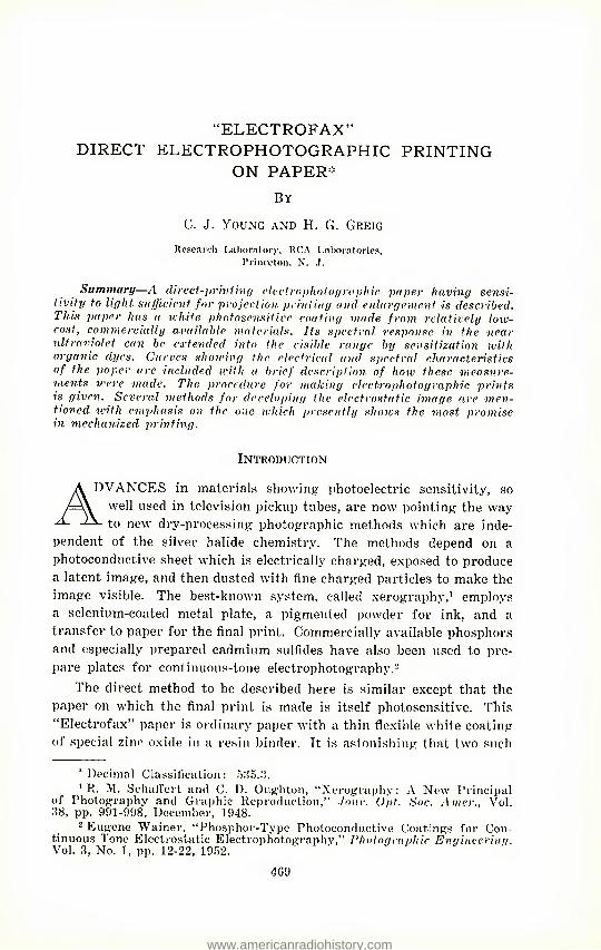
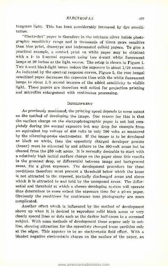
Figure 1 shows the charging apparatus and light source for making prints manually. The "Electrofax" paper is placed on the ground plate and exposed to a corona discharge from one or more fine wires con- nected to a d-c source of 3 to 7 kilovolts negative. The ion flow establishes a charge density on the surface of the paper coating which can be measured as an equivalent surface voltage by a vibrating-probe electrometer (see Appendix). This voltage, initially 300 to 600 volts, decays slowly in the dark over a period of minutes or hours depending on the nature of the coating.
www.americanradiohistory.com
ELECTROFAX 471
During the exposure the charges in the illuminated areas leave the surface in proportion to the amount of incident light. Depending on the conductivity of the supporting paper base, they either remain at the interface or are soon discharged to ground. The developable elec- trostatic image remains on the top surface of the coating.
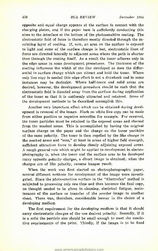
Developing consists in bringing fine positively charged particles of developer powder, or toner, close to the surface, so that they will be
Fig- 1—High-voltage supply, corona-charging unit, ground plate, and light source for making "Electrofax" hand-process prints.
attracted to those areas which are still charged but will not adhere where the charges have moved from the surface due to light exposure.
An effective and practical method has been found for bringing properly charged toner particles to the surface to be developed. It is called magnetic brush development. The "brush" is simply a mass of iron filings mixed with toner and picked up on the end of a per- manent magnet. The iron particles take on negative charges and the
www.americanradiohistory.com
472 RCA REVIEW December lOHJ,
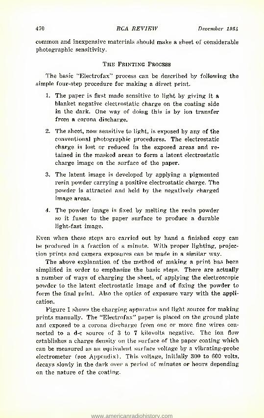
toner particles positive charges by triboelectric effect* when they are mixed. The electrostatic charge latent image on the surface of the paper is revealed with the first sweep of the brush as shown in Fig- ure 2; a few more passes form an image of full density on a clean background. A more detailed discussion of the magnetic brush is given later.
The development of a clean black and white image depends on having a sufficient difference in apparent surface voltage between the
Fig. 2—Hand development of "Electrofax" print with magnetic brush.
charged and the discharged or exposed areas of the latent image. The required difference varies of course with the materials used in the developer. An average value to give clean background is 150 volts.
Voltage drop on exposure can thus be used as a first criterion in comparing the relative sensitivity of various papers, their spectral response, the effects of relative humidity, etc. These factors are con- sidered in more detail in the following section.
* The triboelectric effect may be defined as electrification by contact of two materials having different electron affinities. A triboelectric series is a list of materials empirically arranged so any member will take on a positive charge (lose electrons) on contact with one below it in the series. The triboelectric effect is a surface phenomenon and is therefore influenced by surface conditions which may alter the relative positions of materials in the list.
www.americanradiohistory.com
.y
ELECTROFAX 473
"Electrofax" Papers
As in silver lialide photography, electrophotographic papers can be made to meet the specifications for a particular use. For contact print- ing fiom translucent masters or for projection printing from microfilm where high-contrast black and white copy is desired, the spectral re- sponse of the white zinc-oxide-resin coated papers appears to be tailor-made for the purpose. This paper has good sensitivity to the near ultraviolet below 4200 Angstroms where light sources of both low intensity (fluorescent lamps) for contact printing and of high intensity (mercury arc lamps) for projection printing, are readily available.
Ihe paper can be prepared by conventional paper-coating techniques from a paint-like coating mix of the zinc oxide dispersed in a solution of the resin binder. Viscosity of the mix can be adjusted to meet the requirements of the coater. The paper sheet may be low-cost wood-pulp base or high-strength bond according to the needs.
The electrophotographic paper is comprised of a backing sheet of ordinary paper, sometimes with a clay coating for surface finish, and the finely divided photoconductor dispersed in an insulating binder for the photosensitive layer. Its electrical characteristics are not simple. The moisture content and hence the conductivity of paper varies according to the relative humidity of the air with which it is in equilibrium. The moisture content can vary from 1.8 to 21.5 per cent in the range of relative humidity from 20 to 100 per cent. Paper having about 5-G per cent moisture as normally specified for litho- graphic printing is satisfactory for the base sheet. Good prints can be obtained on the electrophotographic paper, however, over the humidity range 20 to 100 per cent with little modification in processing, and there are practical changes in processing to meet even the driest conditions when the paper becomes a good insulator. Humidity can also have an effect on the electrical charge dark-decay times of the photosensitive coating. This difficulty is overcome by a proper choice from the large number of suitable resin binders.
To gain a better understanding of the printing characteristics of the electrophotographic paper, it is therefore necessary to study the electrical properties of the component parts of the sheet. This is done by following the decay of a surface electrostatic charge with the vibra- ting probe electrometer described in the Appendix. Charge decay on the paper base sheet alone can be followed. The resin binder, without the photoconductor, can be coated on metal and its charge decay determined. With the photosensitive coating on metal, its decay rate both in the dark and upon exposure to light may be plotted. In the
www.americanradiohistory.com
474 HCA REVIEW December lOSJi-
600 £500
RH ■ 40% T = 840F
TIME IN MINUTES
Fig. 3—Voltage decay on charged electrophotographic paper: A) dark decay; B) voltage drop for 1-second exposure with 40-watt incandescent
lamp at 18 inches; C) dark decay after exposure.
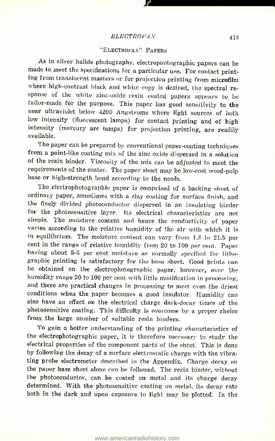
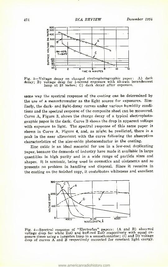
same way the spectral response of the coating can be determined by the use of a monochromator as the light source for exposures. Sim- ilarly, the dark- and light-decay curves under various humidity condi- tions and the spectral response of the composite sheet can be measured. Curve A, Figure 3, shows the charge decay of a typical electrophoto- graphic paper in the dark. Curve B shows the drop in apparent voltage with exposure to light. The spectral response of this same paper is shown in Curve A, Figure 4, and, as might be predicted, there is a peak in the near ultraviolet with the curve following the absorption characteristics of the zinc-oxide photoconductor in the coating.
Zinc oxide is an ideal material for use in a low-cost duplicating paper, because the demands of industry have made it available in large quantities in high purity and in a wide range of particle sizes and shapes. It is nontoxic, being used in cosmetics and ointments and so presents no problem in handling and disposal. Since it remains in the coating on the finished copy, it contributes whiteness and excellent
Kl V" J
'A /C
/ B
WAVCLENGTH.A
Fig. 4—Spectral response of "Electrofax" papers; (A and B) observed voltage drop for white ZnO and buff-red ZnO respectively with equal ex- posure times using a tungsten lamp in a monochromator; (C and D) voltage drop of curves A and B respectively corrected for constant light energy.
www.americanradiohistory.com
ELECTROFAX 475
covering power to the sheet. The eggshell finish of the coating presents a surprisingly good surface for writing with pencil or ink in view of the hydrophobic nature of the resins normally used as binders.
As stated before, the most effective light for printing with the white paper is in the range 3200 to 4200 Angstroms. For reflection piinting, however, where it may be desirable to duplicate a blue signature in a letter, and in many other photographic applications, a much wider response in the visible spectrum is essential. Colored photoconductors with spectral response in the visible range will even- tually find use here. Actually, special zinc oxides are available which in the electrophotographic paper show very good panchromatic re- sponse. The curves in Figure 4 give a comparison of the normal white oxide and a specially prepared reddish-buff colored oxide. An apparent increase in over-all sensitivity of the paper is obtained with the colored oxide. This appears to be due more to increased energy absorp- tion over the wider spectral band than to any increase in intrinsic sensitivity.
Dye Sensitization
For a low-cost duplicating paper, however, a more immediate answer has been discovered which does not presently necessitate the development of special photoconductors to replace the white oxide. It has been found that quite a number of organic dyes can impart a wider spectral response to the white coating. These dyes include many which are unsatisfactory for use in normal silver halide emulsions. The usual restrictions on photographic sensitization where emulsion fogging and interference with development present difficulties, do not apply here because the development is a nonchemical process. Further- more, the poor stability to light exhibited by many dyes is a desirable feature since the white oxide sheet, colored to gain added spectral response, fades again to white with continued exposure of the print to room light. Bleaching of certain other dyes may be accomplished by heat or chemical treatment. Inert coloring media may be incorpo- rated in the sheet for purposes such as color coding or other specific requirements.
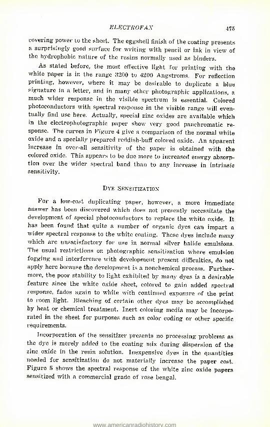
Incorporation of the sensitizer presents no processing problems as the dye is merely added to the coating mix during dispersion of the zinc oxide in the resin solution. Inexpensive dyes in the quantities needed for sensitization do not materially increase the paper cost. Figure 5 shows the spectral response of the white zinc oxide papers sensitized with a commercial grade of rose bengal.
www.americanradiohistory.com
47G RCA REVIEW December 19!H
Fig. 5—Spectral response of rose bengal sensitized "Electrofax" papers, voltage drop corrected for equal light energy.
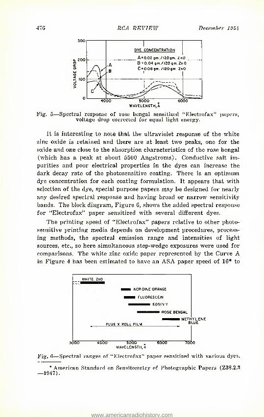
It is interesting to note that the ultraviolet response of the white zinc oxide is retained and there are at least two peaks, one for the oxide and one close to the absorption characteristics of the rose bengal (which has a peak at about 5500 Angstroms). Conductive salt im- purities and poor electrical properties in the dyes can increase the dark decay rate of the photosensitive coating. There is an optimum dye concentration for each coating formulation. It appears that with selection of the dye, special purpose papers may be designed for nearly any desired spectral response and having broad or narrow sensitivity bands. The block diagram. Figure 6, shows the added spectral response for "Electrofax" paper sensitized with several different dyes.
The printing speed of "Electrofax" papers relative to other photo- sensitive printing media depends on development procedures, process- ing methods, the spectral emission range and intensities of light sources, etc., so here simultaneous step-wedge exposures were used for comparisons. The white zinc oxide paper represented by the Curve A in Figure 4 has been estimated to have an ASA paper speed of 16* to
ACRIDINIE ORANGE m FLUORESCEIN hhsmh EOSIN Y
ROSE BENGAL
PLUS X ROLL FILM lMETHYLENE BLUE
6000 WAVELENGTH, A
6000 7000
Fig. 6—Spectral ranges of "Electrofax" paper sensitized with various dyes.
* American Standard on Sensitometry of Photographic Papers (Z38.2.3 -1947).
www.americanradiohistory.com
ELECTROFAX 477
tungsten light. This has been considerably increased by dye sensiti- zation.
"Electrofax" paper is therefore in the intrinsic silver halide photo- graphic sensitivity range and is thousands of times more sensitive than blue print, diazotype and bichromated colloid papers. To give a practical example, a contact print on white paper may be obtained with a 1- to 2-second exposure using two 4-watt white fluorescent lamps at 20 inches as the light source. The setup is shown in F"igure 1. Two 4-watt black-light lamps reduce the exposure to about 1/10 second. As indicated by the spectral response curves, Figure 5, the rose bengal sensitized paper decreases the exposure time with the white fluorescent lamps to about 1 5 second because of the added sensitivity to visible light. These papers are therefore well suited for projection printing and microfilm enlargement with continuous processing.
Development
As previously mentioned, the printing speed depends to some extent on the method of developing the image. One reason for this is that the surface charge on the electrophotographic paper is not lost com- pletely during the normal exposure but may drop for example from an equivalent top voltage of 400 volts to only 250 volts as measured by the vibrating-probe electrometer. If the image is to be developed as black on white, then the oppositely charged developer powder (toner) must be attracted by and adhere to the 400-volt areas but be cleaned from the 250 volt areas. It is normally desirable to start with a relatively high initial surface charge on the paper since this results in the greatest drop, or differential between image and background areas, for a given exposure. The development procedure for these conditions therefore must present a threshold below which the toner is not attracted to the exposed, partially discharged areas and above which it is attracted to and held by the unexposed areas. The differ- ential and threshold at which a chosen developing system will operate thus determines to some extent the exposure time for a given paper. Obviously the conditions for continuous tone photography are more complicated.
Another effect which is influenced by the method of development shows up when it is desired to reproduce solid black areas or very closely spaced lines or dots such as the darker half-tones in a screened subject. With some methods of development these appear only in out- line, showing attraction for the oppositely charged toner particles only at the edges. This appears to be an electrostatic field effect. With a blanket negative electrostatic charge on the surface of the paper, an
www.americanradiohistory.com
478 RCA REVIEW December 195i
opposite and equal charge appears at the surface in contact with the charging platen, and if the paper base is sufficiently conducting this rises to the interface at the bottom of the photosensitive coating. The electrostatic field of force is therefore mostly directed through the in- sulating layer of coating. If, now, an area on the surface is exposed to light and some of the surface charge is lost, electrostatic lines of force are directed laterally to adjacent areas where the path is shorter than through the coating itself. As a result the toner adheres only in the edge areas in some development procedures. The thickness of the coating influences the width of the line developed as does the differ- ential in surface charge which can attract and hold the toner. Where only line copy is needed this edge effect is not a drawback and in some instances may be desirable. Where half-tones and solid areas are desired, however, the development procedure should be such that the electrostatic field is directed away from the surface during application of the toner so that it is uniformly attracted and retained. Some of the development methods to be described accomplish this.
Another very important effect which can be obtained during devel- opment is reversal of the image. Black on white line copy can be made from either positive or negative microfilm for example. For reversal, the toner particles must be retained in the exposed areas and cleaned from the masked areas. This is accomplished by having the original surface charge on the paper and the charge on the toner particles of the same polarity. The toner is then repelled by the like charge in the masked areas and "sees," at least in areas of higher field strength, sufficient attractive force to develop closely adjoining exposed areas. A rough general rule which might be applied to development in electro- photography is, when the toner and the surface area to be developed carry opposite polarity charges, a direct image is obtained; when the charges are of like polarity, reverse images result.
When the work was first started on electrophotographic paper, several different methods for development of the image were investi- gated. Since the photosensitive surface in the "Electrofax" method is subjected to processing only one time and then becomes the final copy, no thought needed to be given to cleaning, electrical fatigue, main- tenance of the surface or transfer of the powder image to another sheet. There was, therefore, considerable leeway in the choice of a developing medium.
The first requirement for the developing medium is that it should carry electrostatic charges of the one desired polarity. Secondly, if it is a solid the particle size should be small enough to meet the resolu- tion requirements of the print. Thirdly, if the image is to be fixed
www.americanradiohistory.com
ELECTROFAX 479
by melting and fusing the toner to the paper and not by some auxiliary treatment, it must melt well below the degrading temperature of the paper (about 1650C).
Five Methods eor Development
One method of obtaining an electrostatic charge on the toner par- ticles is to expose them to ions generated by corona or a radiation source. The most convenient method, however, is by triboelectric effect. The relationship of the two materials in the triboelectric series determines the polarity and to some extent the magnitude of the charge. In the very early experiments with electricity, electroscopic powder mixtures such as sulfur and minium (red lead oxide) were used to show the presence and polarity of electrostatic charges, the sulfur taking on a negative, and the lead oxide a positive charge.
To adapt this technique to electrophotography where only one powder of one polarity is desired on the image, some means for re- moving the second material is needed. In generating a powder cloud this can be by contact with particles too large to go into the cloud, or by impingement where the toner particles are blown repeatedly against baffles or the walls of the cloud chamber made of material having the desired triboelectric properties. It is difficult to generate a powder cloud having particles all charged to one polarity since even pure materials tend to form clouds with some negative and some posi- tive charges. With incomplete charging some means must be found to isolate the particles of the desired polarity for presentation to the paper surface. A grid or electrical field may serve. The powder cloud development of electrophotographic paper prints has been demon- strated.
The problems inherent in dust cloud development apply to liquid spray development as well. Spray techniques, well developed for the paint industry, are presently inefficient for droplet cloud development of electrostatic images. With isolation of the droplets of correct polarity only a small percentage of the ink goes into the image. Clean- ing of the cloud chamber and solvent removal must be considered. This method, however, has the advantage of not requiring an additional step for fixing the image. It would avoid melting and fusing of a powder image which requires considerable power in continuous print- ing. Self-fixing liquid droplet cloud development of electrophotographic paper prints has been demonstrated.
The cascade development method which has been used successfully in xerography,1 utilizes gravity to convey the developer mix across the surface to be developed and to strip the carrier from the developed
www.americanradiohistory.com
480 RCA REVIEW December 195^
image. Here a mixture of beads or granules as the carrier and a very much smaller particle size powder or toner comprise the developer. The carrier and toner gain opposite triboelectric charges by contact during mixing, the materials being chosen to give the desired polarity 'rf charge to the toner. The carrier has the proper shape and mass to permit cascade flow by gravity across the surface to be developed. The surface of course must be inclined to cause the developer to flow and where development is continuous some device is needed to circulate the developer. Electrophotographic paper prints can be developed in this way but the thin flexible sheet does not lend itself to this system as well as does the more rigid metal xerographic plate. The developer mix for use with the paper in direct printing must, of course, be designed to give a positive charge to the toner.
Electrophotographic paper prints have also been developed by ap- plying toner from a roller. This is analogous to planographic printing but the ink (toner powder) sees areas of different electrostatic charge instead of areas of wet hydrophilic ink-repelling surface and dry hydro- phobic ink-receptive surface. Smooth surfaced and grained or knurled metal rollers as well as composition rollers have been used to apply the toner. In most cases the developer roller was run in direct contact with the paper surface to be developed and often with a surprising amount of pressure. When the rollers are conductive, a surface at ground or some desired potential can be presented very close to the charged surface during toner deposition so that the electrostatic field is suitable for the fill-in of solid black areas. The toner is charged either triboelectrically by contact in the feed mechanism and rollers or by ion spray from a corona unit. This method of development is attractive for its mechanical simplicity. With further improvements it may be applied to continuous printing on electrophotographic paper.
The method first mentioned in the description of the printing process, the magnetic brush development, however has given by far the best results both for simple hand processing of electrophotographic paper prints and for adaptation to continuous mechanical development. When a ferromagnetic powder is picked up by a magnet the powder particles arrange themselves in the well known manner along the lines of force in long chains or stacks to simulate the fibers of a brush. This brush structure can be seen in Figure 2. The iron powder, which is low in the triboelectric series, is mixed with a low melting pigmented resin toner that is higher in the: series and so takes on a positive electrostatic charge. This mixture is picked up by a magnet and the resultant brush is swept across the negative electrostatic latent image on the surface to be developed. When the brush passes over a charged
www.americanradiohistory.com
ELECTROFAX 481
area and the electrostatic attraction between the charged toner par- ticles and the oppositely charged image areas is greater than the attraction between the toner and the iron, the toner is stripped from the brush and adheres quite strongly to the paper, forming the visible image. The iron powder is retained in the brush by magnetic attrac- tion. The developer mix is thus handled and brought into position by magnetic forces, while the toner image builds up under electrostatic forces. The selective effect is very definite.
The magnetic brush development method incorporates the advan- tages of efficient triboelectric charging, the presentation of a conduc- tive surface very close to the charged surface facilitating the develop- ment of large black areas, and the positive handling of the developer mix in mechanization. The use of magnetic forces to transport the developer mix and to strip the carrier and unused toner from the paper surface, lends itself to many different approaches for mechanized development. The mass of the carrier can be much less than where gravity alone is the moving force. A relatively small volume of devel- oper mix need be presented to a given area of print to effect develop- ment. This is very desirable for continuous processing.
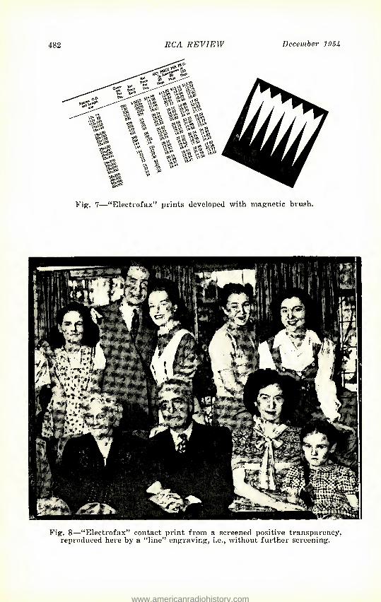
The photosensitive surface of the electrophotographic paper con- sists of very small (0.25-0.35 micron mean diameter) particles of zinc oxide projecting from and surrounded by the insulating binder. The electrostatic surface charges appear to be mostly in the recessed sur- face areas, so it is possible to use conductive metal powders such as iron powder as the carrier in the magnetic brush without removing or degrading the latent image or showing brush traces. The carrier par- ticle size of 25 to 150 microns and the toner particles in the range 25 to 75 microns are both large enough to span several hundred discreet zinc-oxide-resin areas on the paper surface. The toner particle size therefore appears to be the limiting factor in resolution. Legible posi- tive 35-millimeter microfilm contact prints have been made on the "Electrofax" paper by this development method. Figure 7 shows "Elec- trofax" prints illustrating line copy and solid black areas, and Figure 8 shows a screened half-tone, all developed by the magnetic brush method. The actual "Electrofax" copies, after fusing, are as permanent as an impression in printers' ink.
Appendix—Vibrating-Probe Electrometer
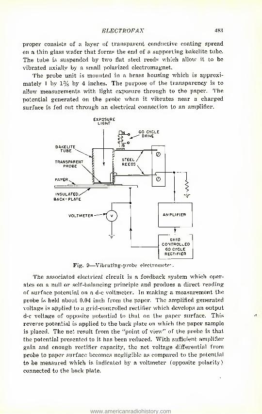
A schematic diagram of the vibrating-probe electrometer used in measuring "Electrofax" paper surface potentials is shown in Figure 9. The device operates on the electrostatic generator principle. The probe
www.americanradiohistory.com
482 RCA REVIEW December l!)5i
Fig. 8—"Electrofax" contact print from a screened positive transparency, reproduced here by a "line" engraving, i.e., without further screening.
www.americanradiohistory.com
ELECTROFAX 483
proper consists of a layer of transparent conductive coating spread on a thin glass wafer that forms the end of a supporting bakelite tube. The tube is suspended by two flat steel reeds which allow it to be vibrated axially by a small polarized electromagnet.
The probe unit is mounted in a brass housing which is approxi- mately 1 by 1% by 4 inches. The purpose of the transparency is to allow measurements with light exposure through to the paper. The potential generated on the probe when it vibrates near a charged surface is fed out through an electrical connection to an amplifier.
BAKELITE TUBE
60 CYCLE DRIVE
VOLTMETER
T GRID
CONTROLLED 60 CYCLE RECTIFIER
Pig. 9—Vibrating-probe electrometer.
The associated electrical circuit is a feedback system which oper- ates on a null or self-balancing principle and produes a direct reading of surface potential on a d-c voltmeter. In making a measurement the probe is held about 0.04 inch from the paper. The amplified generated voltage is applied to a grid-controlled rectifier which develops an output d-c voltage of opposite potential to that on the paper surface. This reverse potential is applied to the back plate on which the paper sample is placed. The net result from the "point of view" of the probe is that the potential presented to it has been reduced. With sufficient amplifier gain and enough rectifier capacity, the net voltage differential from probe to paper surface becomes negligible as compared to the potential to be measured which is indicated by a voltmeter (opposite polarity) connected to the back plate.
www.americanradiohistory.com
484 RCA REVIEW December 1954
This device was used in making measurements for the curves of Figures 3, 4, and 5. In all cases the "Electrofax" paper was first charged with a corona discharge device after which the probe was quickly swung into position. Dark-decay curves resulted from taking a series of readings over a 10-minute period. The spectral response curves resulted from readings taken immediately before and after short exposures to monochromatic light over the ranges indicated.
This vibrating probe electrometer was convenient to use and had a coverage of +1000 volts to —1000 volts in three steps.
Acknowledgment
The authors are particularly indebted to W. H. Bliss for his measurements of paper response, and to R. G. Olden, E. C. Giaimo, and M. L. Sugarman for their work on paper coating techniques, and for triboelectric and photographic studies.
www.americanradiohistory.com
A BRIDGE FOR THE MEASUREMENT OF
CATHODE IMPEDANCE*
By
Robert M. Matheson and Leon S. Nergaard
Research Laboratory, RCA Laboratories, Princeton, N. .1.
Summary—This paper describes a, simple bridge for the measurement of cathode impedance. The bridge compares the unknown tube with a standard tube having an adjustable impedance in the cathode lead. The equivalent circuit of a diode with an oxide cathode is outlined. The choice of standard tubes for use in the bridge is discussed. The method of balanc- ing the bridge is discussed in detail. The circuit diagram of a bridge which has been in use for three years is included together with circuit diagrams of its accessories.
Introduction
conductivity of the oxides of oxide-coated cathodes has long j been of scientific interest.1 However, the degenerative effect of
cathode resistance was of no practical concern in early tubes with their wide electrode spacings and low perveances. With the trend towards close-spaced high-perveance tubes, the cathode resistance became significant and its effect was recognized.2 Recently, the inter- face between the oxide and base metal of a cathode has been recognized as an important source of the degenerative effects observed in com- puter and time-division-multiplex communication applications.3 5
On recognition of the practical importance of cathode impedances, it seemed desirable to have a simple and quick means of measuring
'Decimal Classification: R244.111. 1 A. L. Reimann, Thermionic Emission, Chapman and Hall, Ltd., Lon-
don, 1934. 2 W. R. Ferris, "Some Characteristics of Diodes with Oxide-Coated
Cathodes," RCA Review, Vol. 10, pp. 134-149, March, 1949. 3 Reported at the Tenth Annual Conference on Physical Electronics,
Massachusetts Institute of Technology, 1950: E. S. Rich, "Accelerated Life Test for Cathode-Interface Resistance in Receiving- Type Tubes"; L. S. Nergaard, "Cathode Impedance and Tube Failure"; J. F. Waymouth. Jr., "Deterioration of Oxide Cathodes under Low Duty Factor Operation."
4 J. F. Waymouth, Jr., "Deterioration of Oxide Coated Cathodes under Low Duty Factor Operation," Jour. Appl. Phys., Vol. 22, pp. 80-86, January, 1951.
5 A. Eisenstein, "The Leaky-Condenser Oxide Cathode Interface," Jour. Appl. Phys., Vol. 22, pp. 138-148, February, 1951.
485
www.americanradiohistory.com
486 RCA REVIEW December 19 5^
cathode impedances so that hundreds of tubes could be checked in a routine manner without an undue expenditure of time. The bridge circuit, which is the subject of this paper, was developed to meet this need. The bridge has now been in use for three years and has been found very useful. As will become clear in subsequent discussion, the bridge is not regarded as a precision instrument but as a simple means of obtaining practical data on the cathode impedances of tubes and as a rapid means of acquiring such data on large samples of tubes.
Equivalent Circuit of a Diode
Because tubes are used as circuit elements, it is advantageous to represent them by equivalent circuits; then their performance can be computed in a straightforward engineering manner. Fortunately, the principal nonlinearity of a tube can be assigned to a single element of the equivalent circuit. When a suitable equivalent circuit has been found, it can be used to construct a "synthetic diode" in which the parameters are known, thus providing a standard with which tubes having unknown parameters can be compared. The "standard diode" used in the bridge is such a synthetic diode.
To simplify the exposition, it is advantageous to synthesize the equivalent circuit. The basic circuit element is a perfect diode having no initial electron velocities, no cathode impedance, no contact poten- tials, no anode effects, in fact, having nothing that will cause departures from the Child-Langmuir Law
_ jP1/3/2, v>0 | 0 , F<0
in which
i — anode current
P = perveance
V = anode voltage
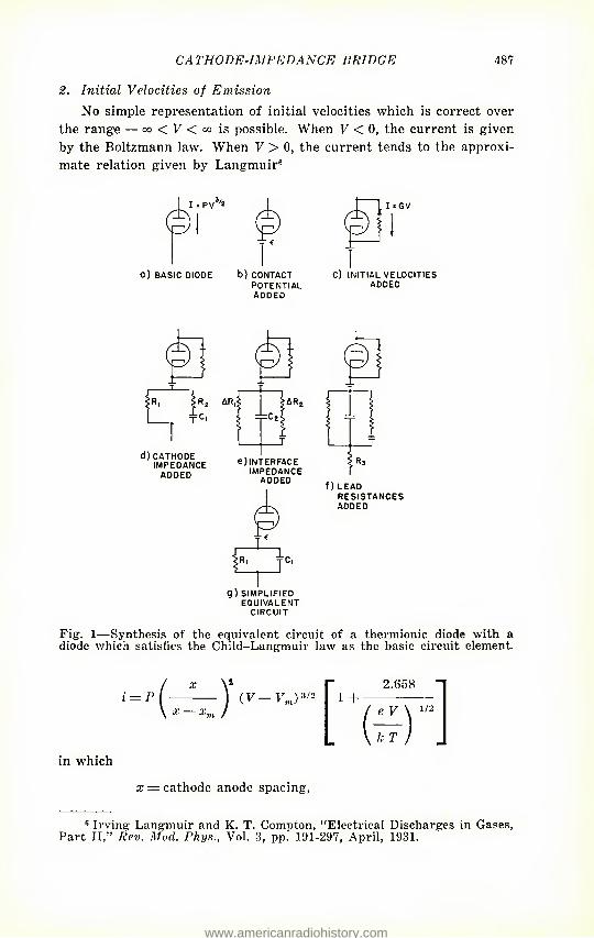
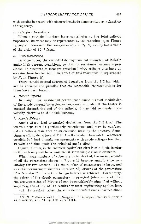
The behavior of this circuit element is characterized by the single parameter P. It now remains to add those circuit elements which cause departures from the 3/2 law. The successive additions are shown in Figure 1.
1. Contact Potentials
The sum of the contact potentials from cathode terminal to anode terminal is represented by a battery as in Figure lb.
www.americanradiohistory.com
CATHODE-IMPEDANCE BRIDGE 487
2. Initial Velocities of Emission
No simple representation of initial velocities which is correct over the range — co < F < =0 is possible. When y < 0, the current is given by the Boltzmann law. When V > 0, the current tends to the approxi- mate relation given by Langmuir6
1 = PV '2
0) BASIC DIODE b) CONTACT POTENTIAL ADDED
I =GV
C) INITIAL VELOCITIES ADDED
d)CATHODE IMPEDANCE
ADDED
<1
<3 O
e) INTERFACE IMPEDANCE
ADDED
g ) SIMPLIFIED EQUIVALENT
CIRCUIT
f) LEAD RESISTANCES ADDED
Fig. 1—Synthesis of the equivalent circuit of a thermionic diode with a diode which satisfies the Child—Langmuir law as the basic circuit element.
x V
X xin j
2.658 1 +•
e 7 \ 1/2
k T
in which
x = cathode anode spacing,
5 Irving Langmuir and K. T. Compton, "Electrical Discharges in Gases, Part II," Rev. Mod. Phys., Vol. 3, pp. 191-297, April, 1931.
www.americanradiohistory.com
488 RCA REVIEW December 19 5 ^
xm = distance from the cathode to the potential minimum,
— potential at the potential minimum,
k = Boltzmann constant,
T = cathode temperature,
e — electronic charge.
This relation pertains to diodes of planar geometry. When 7 > 1 volt, the expression may be approximated by
Experimentally, this relation has proven sufficiently accurate for present purposes for both planar and cylindrical diodes. Hence, the effect of initial velocities can be represented by a conductance in parallel with the perfect diode as shown in Figure 1c. To prevent conduction when F < 0, a diode with a conductance which is large compared with G must be inserted in series with G.
3. Cathode Impedance
Studies of cathode impedance as a function of frequency have shown that this impedance can be represented by the network shown in Figure Id. R2 is usually about five times as great as R1 and the time constant (ftj + R2) Cj is of the order of 1000 microseconds. Unfortunately, R^ R2, and C1 should be nonlinear with voltage. Fur- thermore, they should change rapidly with temperature. What is even worse, they should be time dependent in a manner which depends on past history. It is only when a cathode has been operated under stationary conditions for a considerable time that its parameters are constant in time. These behaviors are difficult to achieve in a synthetic diode. Experience has shown that the values assigned to these param- eters are significant when the average current and the cathode tem- perature at which they are to be used are specified, and that when this specification is made, R1, R.,, and Cj may be used in circuit analysis,
2.658 i = PV3'2 1 +
= PV3'2 + GV, V>1
where
G = 0.752 P
www.americanradiohistory.com
CATHODE-IMPEDANCE BRIDGE ■480
with results in accord with observed cathode degeneration as a function of frequency.
It. Interface Impedance When a cathode interface layer contributes to the total cathode
impedance, its effect may be represented by the capacitor C2 of Figure le, and an increase of the resistances and Kn. C-, usually has a value of the order of 10_a farad.
5. Lead Resistance In some tubes, the cathode tab may run hot enough, particularly
under high current conditions, so that its resistance becomes appre- ciable. In attempts to measure emission limits, cathode tabs have on occasion been burned out. The effect of this resistance is represented by Rz in Figure If.
There remain several sources of departure from the 3/2 law which are so variable and peculiar that no reasonable representations for them have been found.
6. Heater Effects In many tubes, unshielded heater leads cause a small modulation
of the anode current by acting as very-low-mu grids. If the heater is exposed through the end of the cathode, it may add relatively high- velocity electrons to the anode current.
7. Anode Effects Anode effects lead to marked deviations from the 3/2 law.7 The
ten-volt departure is particularly conspicuous and may be confused with a cathode resistance or an emission limit by the unwary. Some- times a slight departure at 2 to 4 volts is also observable. Whenever possible, it is best to make measurements with anode voltages less than 10 volts and thus avoid the principal anode effect.
Figure If, then, is the complete equivalent circuit of a diode insofar as it has been possible to construct it from simple circuit elements.
When large numbers of tubes are to be checked, the measurements of all the parameters shown in Figure If becomes unduly time con- suming for two reasons: ("1) the number of parameters is large, and (2) the measurement involves iterative adjustment of the parameters of a "standard" tube until a bridge balance is achieved. Fortunately, the values of the circuit parameters in practical tubes are such that the representation of Figure If can be considerably simplified without impairing the utility of the results for most engineering applications,
(a) In practical tubes, the equivalent conductance G carries about
7 R. M. Matheson and L. S. Nergaard, "High-Speed Ten-Volt Effect," RCA Review, Vol. XII, p. 258, June, 1951.
www.americanradiohistory.com
490 RCA REVIEW December 195U
20 per cent of the anode current at 10 volts anode voltage. However, when an experimental diode characteristic is plotted on 2 3 power paper, the points fall on an amazingly straight line. It is only when a second diode line at a different cathode temperature is plotted that the effect of the conductance is apparent. It is then obvious that the apparent perveance obtained by running a straight line through ex- perimental points on a 2 3-power plot is a function of temperature, and that the slope of the straight line so obtained is not a direct measure of a true perveance. In routine tests, all of the tubes are run at the same cathode temperature. If the cathode temperature of the standard tube is nearly the same as that of the tubes under test, the conductance G may be omitted from the equivalent circuit and the apparent perveances determined from 2/3-power plots may be used for both the unknowns and the standard.
(b) The capacitance C.z together with resistances and R2 gives a time constant of about 1 microsecond. Hence, when tubes are used at low frequencies the capacitance C2 plays no role. This is equally true of measurements on tubes up to a frequency of the order of 105
cycles. Therefore, for measurements at frequencies below 10® cycles, the capacitance C2 may be omitted from the equivalent circuit.
(c) The resistance R2 is usually 5-10 times as large as R^ Hence, its effect is to reduce the impedance of the cathode circuit 10 to 20 per cent at frequencies above a few kilocycles. As long as this is recog- nized, the omission of R._. leads to no great error. The value of C, obtained by measurement with R., missing is such that C,/?, has about the same value as the time constant C^Rn. The omission of R^ gives a different value of C,. However, C, does not represent a physical capacity, as is apparent from its magnitude (as high as 1 microfarad), so its particular value is of no consequence. It is the time constant C,E, or Ct-Ro which is significant.
(d) The lead resistance R-,, is trivial in most tubes. It is only when very high cathode currents are drawn that it may play a role. Hence, it may be omitted or its effect absorbed in /?, under customary conditions of operation.
When the omissions discussed above are made, the equivalent circuit of Figure Ig results. This circuit is simple, the parameters are easy to determine and for most applications it is adequate. The equivalent circuit of Figure Ig is the one used in the present bridge.
The Bridge Circuit
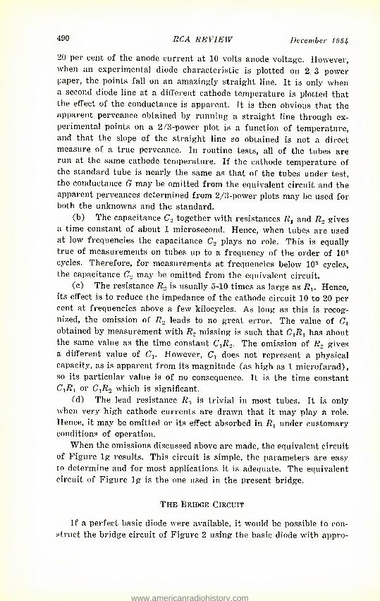
If a perfect basic diode were available, it would be possible to con- struct the bridge circuit of Figure 2 using the basic diode with appro-
www.americanradiohistory.com
CATHODE-IMPEDANCE BRIDGE 491
priate external circuit elements as a synthetic diode with adjustable parameters. Practical solutions to the problem of achieving a satis- factory basic diode are discussed in a later section.
In this circuit, the unknown is characterized by eight parameters. Obviously, the balance indicator and the conditions of operation of the bridge must be such that the unbalance due to improper adjustment of any one of the eight parameters of the standard diode is discernible. Such operation is achieved by operating the bridge on an alternating voltage. Because the basic diode is nonlinear, it generates substantial harmonics. These harmonics are made more pronounced by operating the tubes under Class B conditions, approximately, i.e., without d-c bias other than that due to contact potentials and cathode impedances.
Fig. 2—A bridge circuit for comparing an "unknown" diode with a "stand- ard" synthetic diode. Figure 2a shows the bridge with the circuit of the standard diode detailed; Figure 2b shows the bridge with a condensed
representation of the standard diode.
By using an oscilloscope as an indicator, it is possible, with experience, to adjust the eight parameters properly.
It may be well to note that a meaningful balance is obtained only if the synthetic diode is a proper representation. If the voltage across the diodes exceeds 10 volts, so that the 10-volt effect becomes apparent, or if the counterparts of R1 and R2 are nonlinear, the meaning of balance, if it can be achieved, is dubious. The nature of the 10-volt effect and the variation of the apparent resistances of a cathode with current are such that, if they are present, they prevent achievement of a perfect balance. Furthermore, the variations of the resistances are not characterized by a 3 2 law between current and voltage. Hence, such variations are not masked by the behavior of the basic diode, and their presence is easily detected. The achievement of a practical balance in the presence of these disturbing factors will be discussed later.
The conditions for balance are
STANDARD UNKNOWN 0) COMPLETE REPRESENTATION b) CONDENSED REPRESENTATION
STANDARD UNKNOWN
www.americanradiohistory.com
492 RCA REVIEW December 1954
= e,
_ P, _ _ F,
Gi" PT^X^I7;'
At this point there should be a discussion of the theoretical sensi- tivity and accuracy of the bridge. The fact is that balance of the bridge is possible only because of the nonlinearities involved. These nonlinearities make an analysis difficult and contemplation of the diffi- culties led to the conclusion that the practical benefits to be derived from an analysis would not be commensurate with required expendi- ture of time. Accordingly, no analysis has been made and confidence in the bridge stems from check methods to be described later rather than from theoretical considerations.
Standard Diodes
The ideal standard tube for use in the bridge would have a uni- potential metallic cathode operating at the cathode temperature of the tube to be measured. Then there would be no question of cathode impedance in the standard, no temperature correction and no departure from the Langmuir approximation due to voltage drop along the cathode. Unfortunately, no such tube is readily available. As practical substitutes, the 2V3-G has been used as a primary standard and the 2X2-A as a secondary standard.
The tungsten filament of the 2V3-G has been pulse-heated so that it is a unipotential cathode during the measurement period. The current-voltage characteristic of a 2V3-G is shown in Figure 3. Be- cause the normal cathode temperature of a 2V3-G is about twice that of an oxide cathode, it is necessary to separate out the apparent con- ductance due to initial velocities so that an appropriate correction can be made when an oxide-coated-cathode tube is compared with the 2V3-G. The separation is made as follows: The measured cathode temperature is 2300° K in the present case. Hence, the apparent conductance is
/ 2300 V/2
G = 0.752 PI ) =1.14 P. \1000 /
The ratio of currents carried by the conductance and the ideal 3/2 law diode in the present representation is
1.14 PV 1.14
pys/2 ym
www.americanradiohistory.com
CATHODE-IMPEDANCE DRIDCE 493
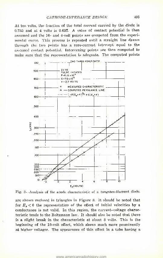
At ten volts, the fraction of the total current carried by the diode is 0.735 and at 4 volts is 0.637. A value of contact potential is then assumed and the 10- and 4-volt points are computed from the experi- mental curve. This process is repeated until a straight line drawn through the two points has a zero-current intercept equal to the assumed contact potential. Intervening points are then computed to make sure that the representation is adequate. The computed points
Fig-. 3—Analysis of the anode characteristic of a tungsten-filament diode.
are shown enclosed in triangles in Figure 3. It should be noted that for Ep < 0 the representation of the effect of initial velocities by a conductance is not valid. In this region, the current-voltage charac- teristic tends to the Boltzmann law. It should also be noted that there is a slight break in the characteristic at about 8 volts. This is the beginning of the 10-volt effect, which shows much more prominently at higher voltages. The appearance of this effect in a tube having a
www.americanradiohistory.com
494 RCA REVIEW December 195i
tungsten emitter is due to the use of a batalum getter. In the applied voltage range between 0 and 8 volts, the representation is adequate and this standard tube is characterized by
P = G.18 x 10^° ampere voIt-3/2
G = 7.0 X 10-° ohm-1
t = 2.7 volts.
While the 2V3-G is, in some ways, a good standard, it is incon- venient to use because the cathode does not operate at a temperature comparable to that normal to oxide cathodes. The inconvenience is illustrated by the calibration of a secondary standard below.
The 2X2-A has been used as a secondary standard. The principal reason for its use is that it has a low perveance so that a cathode resistance of a few hundred ohms does not cause a major departure of the current-voltage characteristic from the ideal. To put the matter in another way, in the bridge a 2X2-A with a cathode resistance of 100 ohms is the equivalent of a 6AG7 with a cathode resistance of about % ohm. One half ohm is a small fraction of the cathode resist- ance normally observed in 6AG7,s (20-300 ohms). While some 2X2-A's, taken from stock, show cathode resistances of 100 ohms or less, the resistance values are likely to range up to 3000 ohms. Hence, a careful selection of the 2X2-A,s to be used as standards is indicated. It is also desirable to age the selected tubes before using them as standards. This has been done by operating them at normal heater voltage with 120 volts a-c on the anode. This usually reduces the initial cathode resistance markedly. A 2X2-A having an initial resistance of 2700 ohms showed a resistance of 350 ohms after 80 hours of aging. It may be desirable to "store" standard 2X2-A's in an aging rack oper- ating under conditions similar to those for the initial aging. This method of "storage" is being tried but it is too early to assess its merits. In any event, it is desirable to check 2X2-A standards periodi- cally to be sure that the cathode resistance has not increased to a point where it causes significant errors in the bridge.
Secondary standards have been calibrated against a 2V3-G. Be- cause this calibration involves a correction for the difference in cathode temperatures, it may be worthwhile to describe the calibration in some detail. Two methods have been used.
1. The 2X2-A is placed in the bridge and both the ratio arm and cathode resistance arm are adjusted successively until the best average balance throughout the a-c cycle is obtained. This process gives tenta- tive values for the perveance and shunt conductance of the 2X2-A.
www.americanradiohistory.com
CATHODE-IMPEDANCE BRIDGE 495
The perveance is obtained directly from the known perveance of the standard and the bridge ratio. The shunt conductance is computed from
where the subscript x refers to the unknown. The shunt conductance of the standard is known. It is the equivalent of a conductance
on the unknown side of the bridge, where a is the bridge ratio. Hence, the unknown must be shunted externally by a conductance
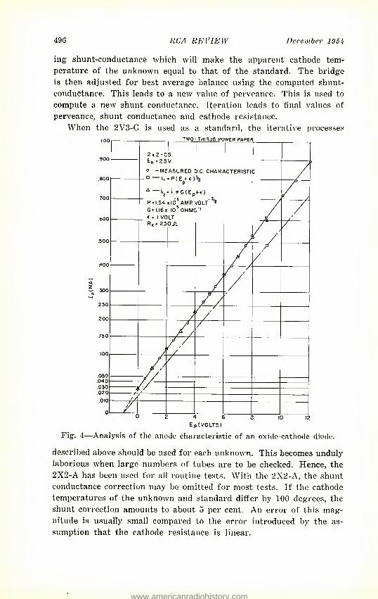
to make its conductance correspond to a cathode temperature equal to that of the standard. This value of conductance is inserted across the unknown tube in the bridge. In practice, the appropriate resistance in series with a 1N39 crystal diode has been inserted so that the base line on the oscilloscope is maintained and so that any charge stored in the cathode circuit does not leak off during the inverse half cycle. The bridge is then adjusted for best average balance again. This yields a new perveance and cathode resistance. Iteration of the correction process yields an excellent balance and final values of the perveance, shunt conductance, and cathode resistance. The current-voltage char- acteristic may then be computed and compared with the measured characteristics of the unknown. Such a comparison is shown in Figure 4. Because the cathode resistance changes the computed current by less than 2 per cent at 9 volts, the cathode resistance has been ignored in Figure 4.
It should be noted that the shunting of a diode by a temperature- correcting shunt conductance is not strictly correct. The shunt con- ductance should be shunted across the cathode-anode space. This is. of course, impossible in a practical diode. If the cathode impedance is small, as it should be in a standard diode, the error caused by connecting the shunt conductance across the entire diode instead of across the cathode-anode space only, is also small.
2. In the alternative method, tentative values of the perveance and the apparent shunt conductance of the unknown are computed from the d-c characteristic, assuming that the cathode resistance is negligible. These values are used to compute the temperature-correct-
G/=Gx,r
G = Gsa-Gx
www.americanradiohistory.com
496 RCA REVIEW December 1954
ing shunt-conductance which will make the apparent cathode tem- perature of the unknown equal to that of the standard. The bridge is then adjusted for best average balance using the computed shunt- conductance. This leads to a new value of perveance. This is used to compute a new shunt conductance. Iteration leads to final values of perveance, shunt conductance and cathode resistance.
Fig. 4—Analysis of the anode characteristic of an oxide-cathode diode.
described above should be used for each unknown. This becomes unduly laborious when large numbers of tubes are to be checked. Hence, the 2X2-A has been used for all routine tests. With the 2X2-A, the shunt conductance correction may be omitted for most tests. If the cathode temperatures of the unknown and standard differ by 100 degrees, the shunt correction amounts to about 5 per cent. An error of this mag- nitude is usually small compared to the error introduced by the as- sumption that the cathode resistance is linear.
www.americanradiohistory.com
CATHODE-IMPEDANCE BRIDGE 497
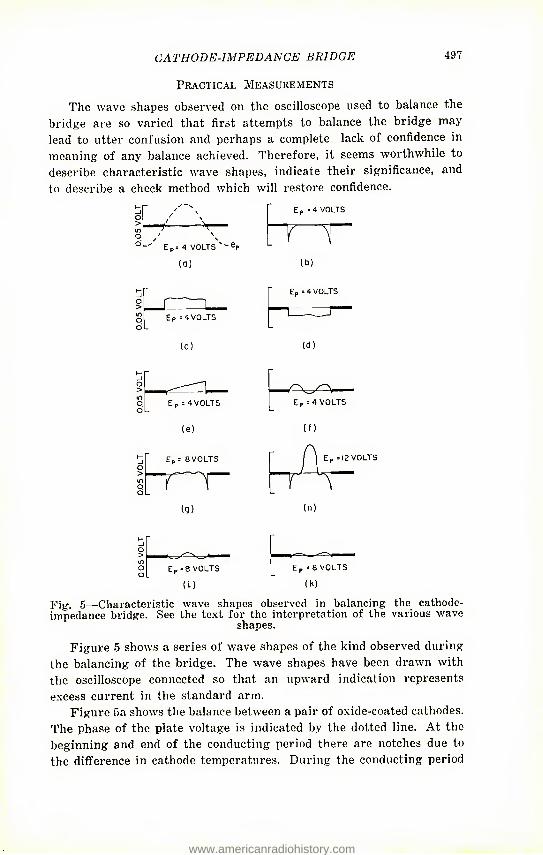
Practical Measurements
The wave shapes observed on the oscilloscope used to balance the bridge are so varied that first attempts to balance the bridge may lead to utter confusion and perhaps a complete lack of confidence in meaning of any balance achieved. Therefore, it seems worthwhile to describe characteristic wave shapes, indicate their significance, and to describe a check method which will restore confidence.
■f- / \ Ep = 4 VOLTS v-eP
(a)
rr^r
(b)
U) (k) pig. 5—.Characteristic wave shapes observed in balancing the_ cathode- impedance bridge. See the text for the interpretation of the various wave
shapes.
Figure 5 shows a series of wave shapes of the kind observed during the balancing of the bridge. The wave shapes have been drawn with the oscilloscope connected so that an upward indication represents excess current in the standard arm.
Figure 5a shows the balance between a pair of oxide-coated cathodes. The phase of the plate voltage is indicated by the dotted line. At the beginning and end of the conducting period there are notches due to the difference in cathode temperatures. During the conducting period
www.americanradiohistory.com
500 RCA REVIEW December 1954-
the perveance of the diode is
I
and the bridge ratio should be
h " ~ p .,'
If the computed value of a does not agree with the value used in balancing the bridge, the initial bridge ratio was incorrect.
If the perveance of the unknown tube is not known with any cer- tainty, it is usually possible to determine the perveance and cathode resistance by iteration of the above measurement and computation. When the iteration is carried out, any one of three possibilities may be encountered;
1. The iteration converges to a definite bridge ratio and cathode resistance. This situation causes no concern.
2. The iteration does not converge to a definite bridge ratio and cathode resistance but to a range of bridge ratios in which the meas- ured cathode resistance is almost independent of the bridge ratio. This situation occurs when the voltage drop across the cathode impedance is comparable to or larger than the vacuum drop. As the vacuum drop becomes smaller relative to the cathode-impedance drop, the principal nonlinearity decreases, and if the vacuum drop becomes negligible and the cathode impedance is linear, the bridge reduces to a simple Wheat- stone bridge and it becomes possible to balance the bridge with any bridge ratio.
3. The iteration fails to converge. This situation occurs when the cathode impedance is nonlinear and the current through the unknown is not held constant. It is not sufficient to hold the bridge current constant because the current division in the bridge changes as the bridge ratio is changed. This situation also occurs when the cathode impedance is not stable. Both oxide impedance and interface impedance are mai-kedly affected by current, particularly by currents larger than those at which a measurement is to be made. If a cathode is subjected to a considerable excess current, the cathode impedance will drift for a considerable time thereafter. It is impossible to iterate bridge ad- justment in the presence of such a drift. Because nonconvergence is so distressing when first encountered, it seems worthwhile to stress that the current change due to a change in bridge ratio may change the cathode impedance enough so that the iteration process fails to
www.americanradiohistory.com
CATHODE-IMPEDANCE BRIDGE 501
converge. The difficulty lies in the nature of the cathode impedance, not in the bridge.
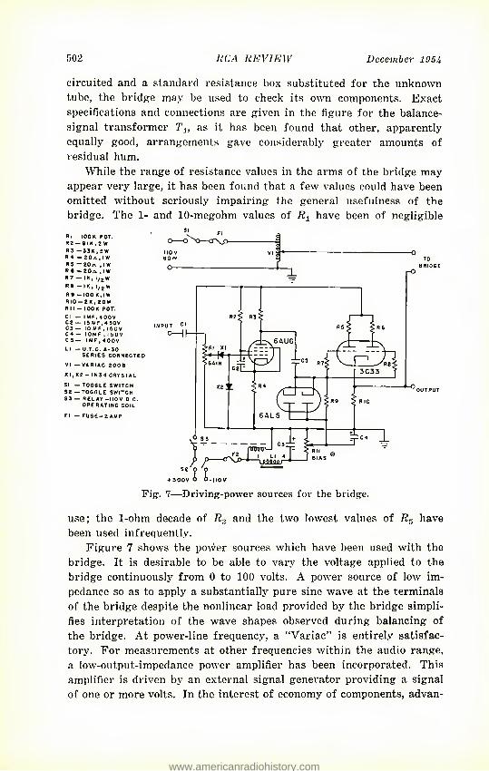
Detailed Circuits
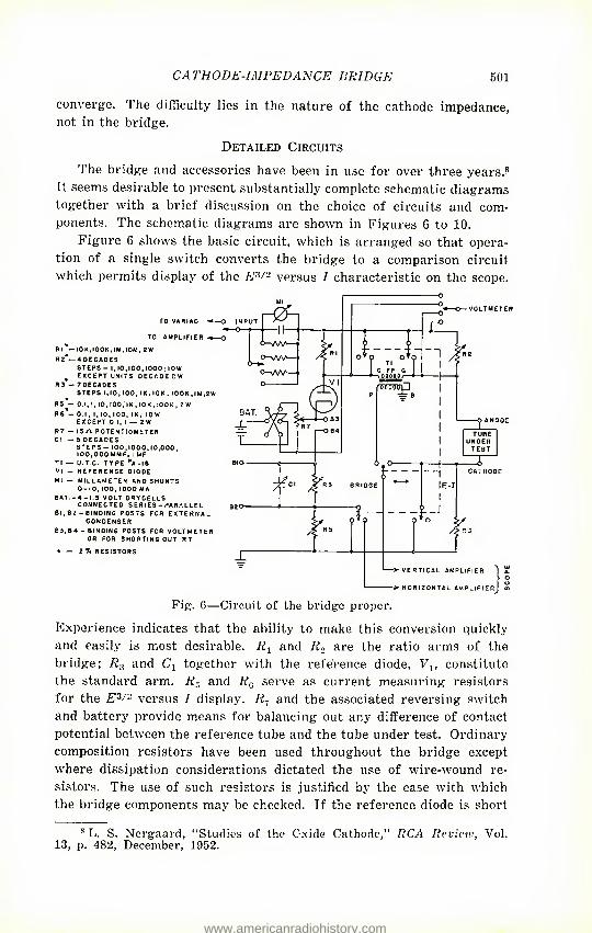
The bridge and accessories have been in use for over three years.? It seems desirable to present substantially complete schematic diagrams together with a brief discussion on the choice of circuits and com- ponents. The schematic diagrams are shown in Figures 6 to 10.
Figure 6 shows the basic circuit, which is arranged so that opera- tion of a single switch converts the bridge to a comparison circuit which permits display of the Z?3/2 versus 1 characteristic on the scope.
Experience indicates that the ability to make this conversion quickly and easily is most desirable. and R-^ are the ratio arms of the bridge; and C1 together with the reference diode, Vu constitute the standard arm. R- and R0 serve as current measuring resistors for the E3/~ versus I display. R-j and the associated reversing switch and battery provide means for balancing out any difference of contact potential between the reference tube and the tube under test. Ordinary composition resistors have been used throughout the bridge except where dissipation considerations dictated the use of wire-wound re- sistors. The use of such resistors is justified by the ease with which the bridge components may be checked. If the reference diode is short
8 L. S. Nergaard, "Studies of the Cxide Cathode," RCA Review, Vol. 13, p. 482, December, 1952.
www.americanradiohistory.com
502 RCA REVIEW December 195Jt
circuited and a standard resistance box substituted for the unknown tube, the bridge may be used to check its own components. Exact specifications and connections are given in the figure for the balance- signal transformer Tu as it has been found that other, apparently equally good, arrangements gave considerably greater amounts of residual hum.
While the range of resistance values in the arms of the bridge may appear very large, it has been found that a few values could have been omitted without seriously impairing the general usefulness of the
use; the 1-ohm decade of K3 and the two lowest values of R6 have been used infrequently.
Figure 7 shows the power sources which have been used with the bridge. It is desirable to be able to vary the voltage applied to the bridge continuously from 0 to 100 volts. A power source of low im- pedance so as to apply a substantially pure sine wave at the terminals of the bridge despite the nonlinear load provided by the bridge simpli- fies interpretation of the wave shapes observed during balancing of the bridge. At power-line frequency, a "Variac" is entirely satisfac- tory. For measurements at other frequencies within the audio range, a low-output-impedance power amplifier has been incorporated. This amplifier is driven by an external signal generator providing a signal of one or more volts. In the interest of economy of components, advan-
www.americanradiohistory.com
CATHODE-IMPEDANCE BRIDGE 503
tage has been taken of the fact that the bridge requires power during only the positive half cycle.
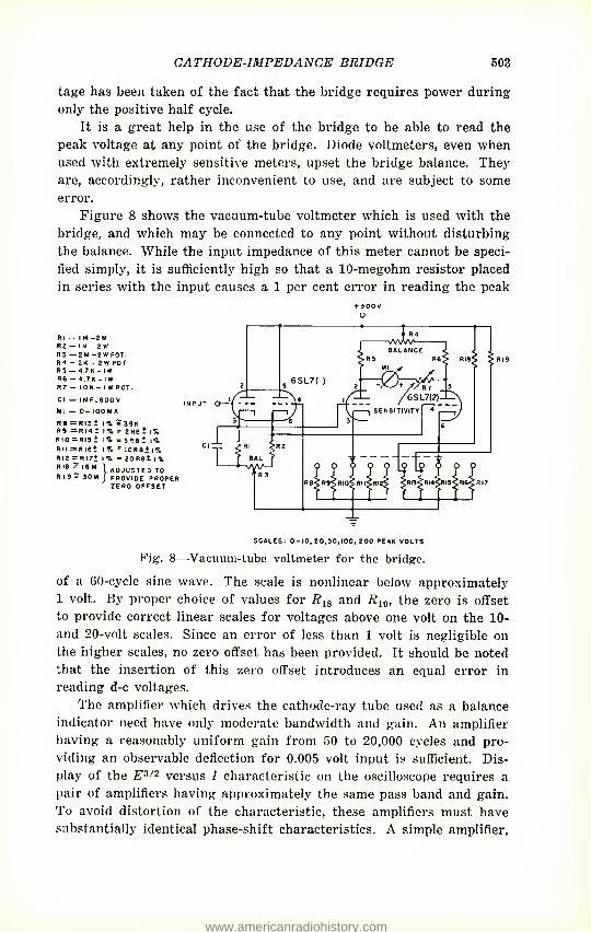
It is a great help in the use of the bridge to be able to read the peak voltage at any point of the bridge. Diode voltmeters, even when used with extremely sensitive meters, upset the bridge balance. They are, accordingly, rather inconvenient to use, and are subject to some error.
Figure 8 shows the vacuum-tube voltmeter which is used with the bridge, and which may be connected to any point without disturbing the balance. While the input impedance of this meter cannot be speci- fied simply, it is sufficiently high so that a 10-megohm resistor placed in series with the input causes a 1 per cent error in reading the peak
• I M —2 W - I M - 2 W -2M — 2 W POT. - 2 K - 2 W POT. - 4 .7 K - I W - 4 7K -IW - 10 K - I W POT. -IMF 00 V
00 M A R8 = RI3 1 I % 5 R9 ' I 0 :
RI 9 = 30 M
3 9 K R 14 t 17.= 2 R0 t I % RI5 + 1% = 5R8 t \1. R 16 t l7o=lOR8+l7. R I7t I % = 20 R8± I 7. 16 M I ADJUSTED TO J PROVIDE PROPER ZERO OFFSET
SCALES 0- 10, 20,50,100, 200 PEAK VOLTS Fig-. 8—Vacuum-tube voltmeter for the bridge.
of a 60-cycle sine wave. The scale is nonlinear below approximately 1 volt. By proper choice of values for R1S and R^, the zero is offset to provide correct linear scales for voltages above one volt on the 10- and 20-volt scales. Since an error of less than 1 volt is negligible on the higher scales, no zero offset has been provided. It should be noted that the insertion of this zero offset introduces an equal error in reading d-c voltages.
The amplifier which drives the cathode-ray tube used as a balance indicator need have only moderate bandwidth and gain. An amplifier having a reasonably uniform gain from 50 to 20,000 cycles and pro- viding an observable deflection for 0.005 volt input is sufficient. Dis- play of the E?'/'1 versus I characteristic on the oscilloscope requires a pair of amplifiers having approximately the same pass band and gain. To avoid distortion of the characteristic, these amplifiers must have substantially identical phase-shift characteristics. A simple amplifier.
www.americanradiohistory.com
504 RCA REVIEW December 195U
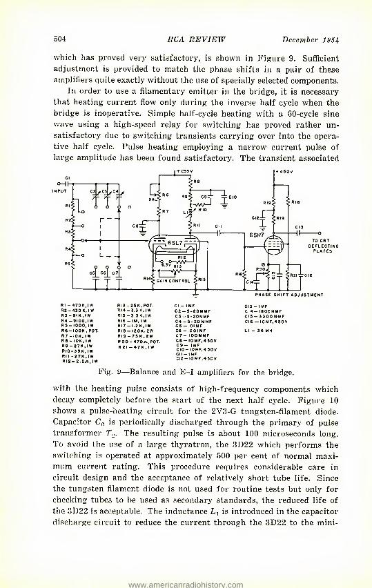
which has proved very satisfactory, is shown in Figure 9. Sufficient adjustment is provided to match the phase shifts in a pair of these amplifiers quite exactly without the use of specially selected components.
In order to use a filamentary emitter in the bridge, it is necessary that heating current flow only during the inverse half cycle when the bridge is inoperative. Simple half-cycle heating with a 60-cycle sine wave using a high-speed relay for switching has proved rather un- satisfactory due to switching transients carrying over into the opera- tive half cycle. Pulse heating employing a narrow current pulse of large amplitude has been found satisfactory. The transient associated
TO CRT DEFLECTING PLATES
R I - 470 K, I W R2- 430 K, I W R3 - 91 K . I W R4 -9100, I W R 5 — 1000, IW R6 - I00K , POT. R 7 - 10 K , I W R 8 - I0K , I W R 9 — 2 7 K , I W R 10 - 3 9 K, I W R I I - 2 7 K , 1W R 12- 2 .2/1, I W
R I 3 - 2 5 K , POT. RI4 - 3.3 K, I W RI5 - 3.3 K, I W R16 - IM, I W R 17 —1.2 K , I W RI8 — I20K,2W RI9 —75 K,2W R 20- 4 70 /v, POT. R 21 - 47 K . I W
Cl - IMF C 2 —5-20MMF C 3 -5-20MMF C 4 - 5 - 20 MMF C 5 — .01 MF C6 - .001 MF 07- I00MMF C 8 — 10 M F, 4 50 V C 9 — IMF CIO- 10 MF, 4 50 V CM - IMF CI2 — I0MF,450V
j ^ri n
K ITT I PHASE SHIFT ADJUSTMENT Cl 3 — IMF C 14— I 8 00 MMF CI5 — 3300MMF CIS — I 0 M F, 4 50 V LI - 36 MH
Fig. 9—Balance and E-I amplifiers for the bridge.
with the heating pulse consists of high-frequency components which decay completely before the start of the next half cycle. Figure 10 shows a pulse-heating circuit for the 2V3-G tungsten-filament diode. Capacitor Cc, is periodically discharged through the primary of pulse transformer T2. The resulting pulse is about 100 microseconds long. To avoid the use of a large thyratron, the 3D22 which performs the switching is operated at approximately 500 per cent of normal maxi- mum current rating. This procedure requires considerable care in circuit design and the acceptance of relatively short tube life. Since the tungsten filament diode is not used for routine tests but only for checking tubes to be used as secondary standards, the reduced life of the 3D22 is acceptable. The inductance Lj is introduced in the capacitor discharge circuit to reduce the current through the 3D22 to the mini-
www.americanradiohistory.com
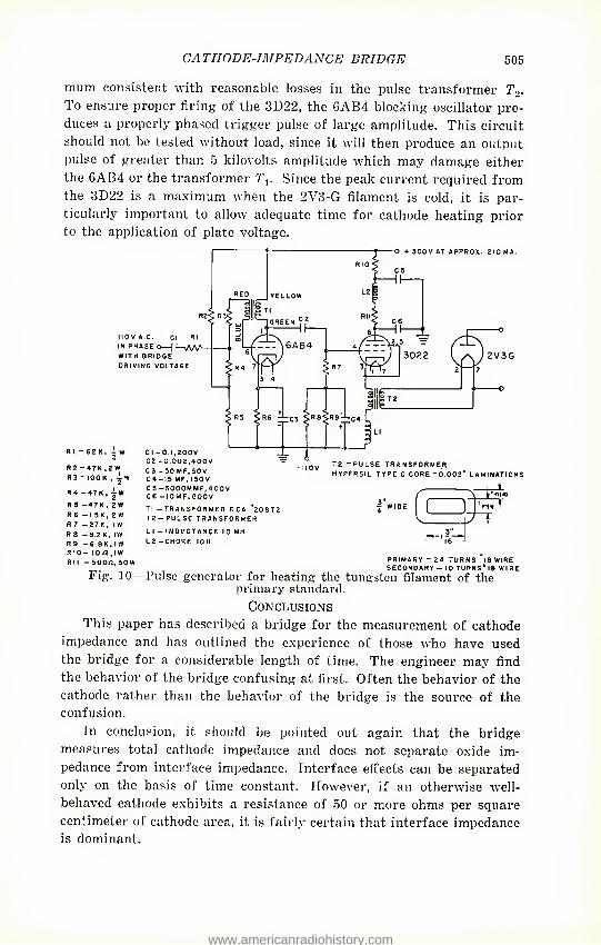
CA THODE-IMPEDANCE BRIDGE 505
mum consistent with reasonable losses in the pulse transformer T2. To ensure proper firing of the 3D22, the 6AB4 blocking oscillator pro- duces a properly phased trigger pulse of large amplitude. This circuit should not be tested without load, since it will then produce an output pulse of greater than 5 kilovolts amplitude which may damage either the 6AB4 or the transformer Tv Since the peak current required from the 3D22 is a maximum when the 2V3-G filament is cold, it is par- ticularly important to allow adequate time for cathode heating prior to the application of plate voltage.
■O + 300VATAPPR0X. 2IOMA.
IIOVA.C. Cl R IN PHASE O j {-vVNA WITH BRIDGE DRIVING VOLTAGE
R 2 -47K ,2 W R3 - IOOK , -iw R 4 - 47 K , — W R 5 -47 K , 2 W R 6 — 1.5 K , 2 W R 7 — 27 K, I W R 8 -0.2 K, IW R 9 - 6 .8 K , IW RIO- 10/2 ,1 W Rll - 500/1,SOW
Cl -0.1,200V C2 -0.002,400V — C 3 - 50 M F, 50 V C 4 - 15 MF, 150V C 5 -5000MMF, 400V ce -lOMF.GOOV TI -TRANSFORMER RCA "208T2 T2 — PULSE TRANSFORMER LI - INDUCTANCE 10 MH L 2 -CHOKE 10 H
T 2 "PULSE TRANSFORMER HYPERSIL TYPE C CORE "0 002" LAMINATIONS
WIDE ( 1" 7J
- T
PRIMARY — 24 TURNS I8WIRE SECONDARY — 10 TURNS* 18 WIRE
Fig-. 10—Pulse generator for heating the tungsten filament of the primary standard.
Conclusions This paper has described a bridge for the measurement of cathode
impedance and has outlined the experience of those who have used the bridge for a considerable length of time. The engineer may find the behavior of the bridge confusing at first. Often the behavior of the cathode rather than the behavior of the bridge is the source of the confusion.
In conclusion, it should be pointed out again that the bridge measures total cathode impedance and does not separate oxide im- pedance from interface impedance. Interface effects can be separated only on the basis of time constant. However, if an otherwise well- behaved cathode exhibits a resistance of 50 or more ohms per square centimeter of cathode area, it is fairly certain that interface impedance is dominant.
www.americanradiohistory.com
STUDY OF P-N-P ALLOY JUNCTION TRANSISTOR FROM D-C
THROUGH MEDIUM FREQUENCIES*
By
L. J. Giacoletto
Research Laboratory, RCA Laboratories, Princeton, N. J.
Summary—With the increase in commercial importance of transistors, it has become necessary that the various factors that enter into the con- struction of a transistor he ascertained and delineated. This study was undertaken with the object of arriving at various relationships which could be used in the design of transistors of predetermined characteristics. Al- though d-c characteristics were measured and studied, the main emphasis is on small-signal operation. Detailed measurements were made of a junc- tion transistor, and these measurements are compared with theoretical calculations. Existing theories are modified and extended as it appears necessary. Various measurements are used to evaluate important constants of the mnterials used and the dimensions involved.
Generally, good agreement is found between theory and measurements. It should accordingly be feasible to carry out a large part of the design of a transistor without recourse to the construction of devices. In addition, the manner in which the transistor operation is dependent upon operating voltage, current, frequency, and temperature can be predicted within a workable degree of accuracy so that both device and circuit designers can carry out the calculations necessary to obtain the answers desired.
Introduction
THE main purpose of this study is to determine suitable design equations for alloy junction transistors. For this purpose it is necessary to ascertain how well a p-n-p alloy junction transistor
fits the theory developed by Shockley and by Shockley, Sparks, and Teal1 for grown junction transistors. The theories developed by these authors will hereafter be lumped together and referred to as Shockley's theory. Refinements and extensions of Shockley's theory will also be introduced and used as required.
When the alloy junction transistor was developed,2 it was not clear that its operation would be similar to that of a grown junction tran-
* Decimal Classification: R282.12. 1 W. Shockley, "The Theory of P-N Junctions in Semiconductors and
P-N Junction Transistors," Bell Sys. Tech. Jour., Vol. 28, pp. 435-489, July, 1949; W. Shockley, M. Sparks and G. K. Teal, "P-N Junction Transis- tors," Phys. Rev., Vol. 83, pp. 151-162, July 1, 1951.
2 R. R. Law, C. W. Mueller, J. I. Pankove, and L. Armstrong, "A De- velopmental Germanium P-N-P Junction Transistor," Proc. I.R.E., Vol. 40, pp. 1352-1357, November, 1952.
506
www.americanradiohistory.com
ALLOY JUNCTION TRANSISTOR 507
sistor. This uncertainty was due to the fact that the emitter and collector semiconductors could not be delineated nor could their electrical constants be specified. During the course of this study it became apparent that the two types of transistors, although different in some details, were very similar in fundamental aspects. Con- comitantly with this study, there has been a growing realization that the alloying process produces emitter and collector semiconductors by recrystallization of heavily doped germanium upon the original ger- manium crystal.3 These emitter and collector end sections are generally very thin — of the order of 1 mil. Methods have not as yet been developed for determining accurately the electrical constants of the end sections, although some approximate results will be discussed. Suitable electrical constants of the end sections are required if the junction transistor design is to be carried out in detail in accordance with the formulation of this paper.
This study of the p-n-p alloy transistor indicates that Shockley's theory holds reasonably well when applied to the true intrinsic tran- sistor. In addition to the intrinsic transistor there are certain extrinsic elements which must be included in the description of the complete device. The terms intrinsic and extrinsic are employed here in their general meaning (belonging to or not belonging to the essence of the thing) and have no connection with their limited application describing materials (intrinsic and extrinsic semiconductors). The most impor- tant of these extrinsic elements is a base-lead resistance. This base- lead resistance has an important effect in determining the over-all performance of the device. The next important extrinsic element is a shunt conductance across the collector junction. This conductance probably arises from surface leakage at the place where the collector junction meets the surface. The leakage conductance is closely related to transistor life, temperature and time stability, and noise, which factors are not considered in this study. Neither the base-lead resist- ance nor the leakage conductance have been completely formulated analytically so their values must generally be determined by measure- ments.
The Shockley analysis utilizes the assumption that the density of the minority carriers is much smaller than the density of majority carriers. This assumption is valid only for relatively small currents. Thus for the transistor under study, the minority carrier density at the emitter becomes equal to the base majority carrier density at an emitter current of 0.42 milliampere (emitter current density = 0.5 ampere/cm3). Despite the breakdown in this basic assumption, the
3 J. I. Pankove, "Recrystallization of Germanium from Indium Solution," RCA Review, Vol. 15, pp. 75-85, March, 1954.
www.americanradiohistory.com
508 RCA REVIEW December 195i
discrepancies that arise do not appear to be serious within the scope of this study. For still larger current density operation the discrep- ancies can no longer be overlooked, and Shockley's analysis must be modified.15
The main emphasis throughout this study is upon the transistor as a device and the determination of suitable design equations therefor. In a sense, however, this study must be considered a progress report, as there is much measurement and analysis work needed before all aspects of the transistor device are completely determined. However, the important properties of the transistor can be determined by suit- able equations so that design work can proceed with assurance.
D-C Characteristics
Analytic Formulation Before investigating the a-c operation of the transistor, it is
instructive to study the d-c operation. This starting point is par- ticularly desirable since the low-frequency resistive parameters are related to the variation of the d-c quantities. The constructional details of the p-n-p alloy junction transistor that is to be considered herein are shown in Figure 1 drawn approximately to scale with the major dimensions shown.2
According to the Shockley theory, the d-c characteristics of a junction transistor can be written in a linear form using some derived voltages as the variables. Thus,
Iir = Oe'E' ^E'lf + flVc -Sc'C' > (1)
Ic =: 9c'E' BE II' + Sec Bcif >
where /,7. = emitter and collector currents respectively
Oe'e i Se'c Sc'e'< Svc = input, reverse transfer, forward transfer, and output d-c conductance coefficients, respec- tively,
and the derived voltage variables are defined as
1 Be'B- = [l-eAtW], (2)
A 4 W. van Roosbroeck, "Theory of the Plow of Electrons and Holes in
Germanium and Other Semiconductors," Bell Sys. Tech. Jour., Vol. 29, pp. 560-607, October, 1950, and "The Transport of Added Current Carriers in a Homogeneons Semiconductor," Phys. Rev., Vol. 91, pp. 282-289, July, 1953.
5 W. M. Webster, "On the Variation of Junction-Transistor Current- Amplification Factor with Emitter Current," Proc. I.R.E., Vol. 42, pp. 914- 920, June, 1954.
www.americanradiohistory.com
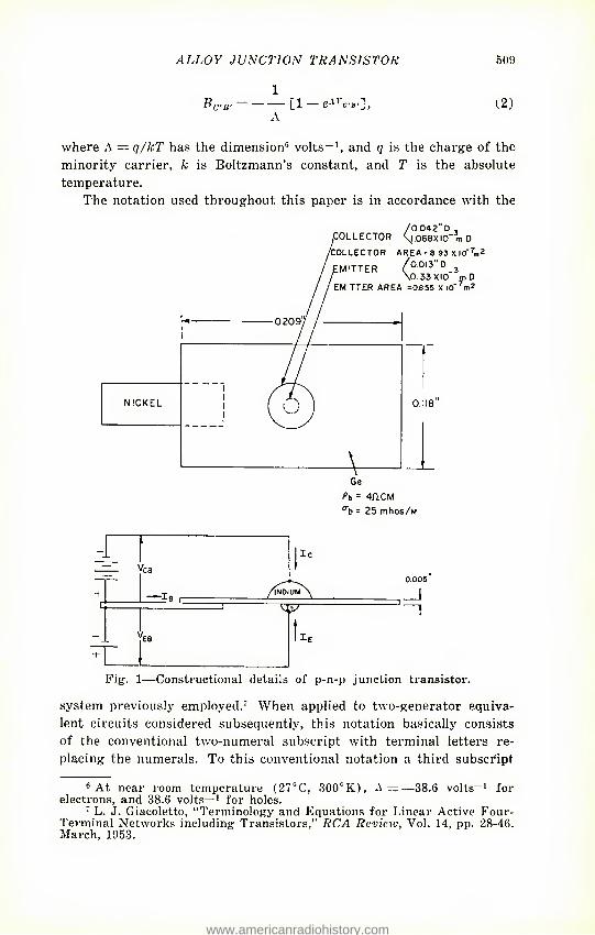
ALLOY JUNCTION TRANSISTOR 509
1
A /W= [1 — eArr'j)'], (2)
where A = q/kT has the dimension6 volts^1, and q is the charge of the minority carrier, k is Boltzmann's constant, and T is the absolute temperature.
The notation used throughout this paper is in accordance with the
/0,042" D , ^COLLECTOR \l,068XI0~^n D
'COLLECTOR AREA = e.93XIO"7m2 MITTER ^00I3"D_3 33X10 mD
EMITTER AREA =0,855 X IO"7m2
Ge ^1,= 4ACM ab = 25 mhos/fn
Pig. 1—Constructional details of p-n-p junction transistor.
system previously employed.7 When applied to two-generator equiva- lent circuits considered subsequently, this notation basically consists of the conventional two-numeral subscript with terminal letters re- placing the numerals. To this conventional notation a third subscript
6 At near room temperature (270C, 300oK), A——38.6 volts—1 for electrons, and 38.6 volts—1 for holes.
7 L. J. Giacoletto, "Terminology and Equations for Linear Active Pour- Terminal Networks including Transistors," RCA Review, Vol. 14, pp. 28-46. March, 1953.
www.americanradiohistory.com
510 RCA REVIEW December 195i
has been added which designates the common terminal between the input and output circuit. Thus y,.^ is the transfer admittance to the collector from the emitter in a common-base circuit. If only one circuit connection is being considered, or if no ambiguity arises, the last subscript designating the common electrode may be omitted as is done above for the d-c conductance coefficients. When applied to the single- generator equivalent circuit, a presubscript designates the common electrode between the input and output circuits, and the two post- subscripts designate the terminals between which the admittance is located. Thus cybr, is the admittance between the base and the emitter in a common-collector circuit. The generator parameter is designated by the postsubscript m.
The symbol "e" in Equations (2) is the base of Napierian log- arithms. In these equations, as well as some that follow, "prime" notations are used to indicate that the quantities relate to "intrinsic" transistor. Capital letter subscripts are used to denote d-c quantities. In later equations, lower case subscripts are used to denote a-c quan- tities. The d-c conductance coefficients in Equation (1) are similar to perveance coefficients employed in electron-tube studies.
Equations (1) and (2) can be combined and written in the form:
The d-c coefficients, IE'E-, Ie'c^ etc. are the corresponding d-c conduct- ance coefficients divided by A, that is, IE.K. = etc. lK.s and /p S
are the emitter and collector saturation currents that flow due to thermally generated electron-hole pairs when both junctions are biased into saturation in the reverse direction. These saturation currents are
The base current can be obtained with the aid of Equation (3) as
I If = [ (I K' It' + (I EX" + ^CX") > (5)
IE' I E'S — + I
Ic' — 1c's = \ I vE'eKr f3)
(4)
where
I K'S — (IE'S + -^cs) — f E'E' + IvE' + •TE'C + Icc-
Since the d-c conductance coefficients represent measurements of the transistor as a passive device, i.e., d-c biasing voltages and currents are
www.americanradiohistory.com
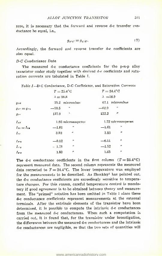
ALLOY JUNCTION TRANSISTOR 511
zero, it is- necessary that the forward and reverse d-c transfer con- ductance be equal, i.e.,
Qn'C'== Oc'E'- '7)
Accordingly, the forward and reverse transfer d-c coefficients are also equal.
D-C Conductance Data The measured d-c conductance coefficients for the p-n-p alloy
transistor under study together with derived d-c coefficients and satu- ration currents are tabulated in Table I.
Table I—D-C Conductance, D-C Coefficients, and Saturation Currents T = 25.4 0C r = 24.4<>C A —38.8 A =38.9
gEE 75.2 mjcromhos 67.1 micromhos
-i/.r —70.5 " —62.9 ffrr 137.0 " 122.2
I„K 1.93 microamperes 1.72 microamperes
Ir.o = Ic, —1.81 " —1.61 Ira 3.52 " 3.13
h.s —0.12 " —0.11 —1.71 " —1.52
/„■„ 1.83 " 1.63
The d-c conductance coefficients in the first column (r = 25.40C) represent measured data. The second column represents the measured data corrected to 71 = 24.40C. The lower temperature was employed for the measurements to be described. As Shockley1 has pointed out, the d-c conductance coefficients are exceedingly sensitive to tempera- ture changes. For this reason, careful temperature control is manda- tory if good agreement is to be obtained between theory and measure- ment. The "primed" notation has been omitted in Table I since these d-c conductance coefficients represent measurements at the external terminals. After the extrinsic elements of the transistor have been determined, it is possible to compute the intrinsic d-c conductances from the measured d-c conductances. When such a computation is carried out, it is found that, for the transistor under investigation, the differences between the measured d-c conductances and the intrinsic d-c conductances are negligible, so that the two sets of quantities will
www.americanradiohistory.com
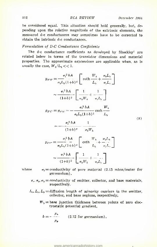
512 RCA REVIEW December 195i
be considered equal. This situation should hold generally, but, de- pending upon the relative magnitude of the extrinsic elements, the measured d-c conductances may sometimes have to be corrected to obtain the intrinsic d-c conductances.
Formulation of D-C Conductance Coefficients The d-c conductance coefficients as developed by Shockley1 are
related below in terms of the transistor dimensions and material properties. The approximate expressions are applicable when, as is usually the case, Wb/Lb « 1.
bA
it,,Li, (1 + ^) '
af bA
IT7
coth L
(1+b)- L "b W,.
(ji- bA flc-E' =
"hLi, (l+b)2
CT;- bA 1
1 b V Lr
1 "
(TrL(, _
wh csch —
L h (8)
dc:
(l+b)2
a,2 hA
<xhLh{i+by-1_
cr,2 bA
r
T.W,,
W„ coth h
L,, ]
(l+b)- —+—1
where o-j = conductivity of pure material (2.13 mhos/meter for germanium),
(t,,, ctc, (xfj = conductivity of emitter, collector, and base materials, respectively.
Lr, L,., Lh — diffusion length of minority carriers in the emitter, collector, and base regions, respectively,
W,, — base junction thickness between points of zero elec- trostatic potential gradient,
b = - Hn
1-LP (2.12 for germanium),
www.americanradiohistory.com
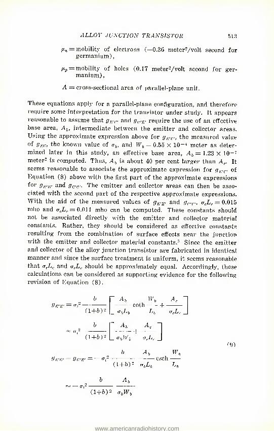
ALLOY JUNCTION TRANSISTOR 513
P-n — mobility of electrons (—0.36 meter2/volt second for germanium),
— mobility of holes (0.17 meter2/volt second for ger- manium) ,
A = cross-sectional area of parallel-plane unit.
These equations apply for a parallel-plane configuration, and therefore require some interpretation for the transistor under study. It appears reasonable to assume that and flV"/?' require the use of an effective base area, Ah, intermediate between the emitter and collector areas. Using the approximate expression above for gE.c., the measured value
of 9Ea> the known value of a,,, and Wil = 0.55 X 10meter as deter- mined later in this study, an effective base area, Ab = 1.23x U)-7
meter2 is computed. Thus, A,, is about 40 per cent larger than Ar. It seems reasonable to associate the approximate expression for gr/c of Equation (8) above with the first part of the approximate expressions for gand gC'0: The emitter and collector areas can then be asso- ciated with the second part of the respective approximate expressions. With the aid of the measured values of gE.E, and <7r.r., a,.Lr = 0.015 mho and o^.L,. = 0.011 mho can be computed. These constants should not be associated directly with the emitter and collector material constants. Rather, they should be considered as effective constants resulting from the combination of surface effects near the junction with the emitter and collector material constants.5 Since the emitter and collector of the alloy junction transistor are fabricated in identical manner and since the surface treatment is uniform, it seems reasonable that ffpL,. and <rcL,. should be approximately equal. Accordingly, these calculations can be considered as supporting evidence for the following revision of Equation (8).
g e'E' = "r — (1+5)2
b ^ (T~ —
(1+5)2
g lye ~ g(;■];■
A„ Wb A,, coth f -
'Ti,Lh Lh (j(,Lr _
Ab -4,,
_ abV/„ <t(,L,
b A i, Wb — csch —
(l+b)2 cr,,Lf, Lh
Ah
(1 + b)2 cr^Wf,
www.americanradiohistory.com
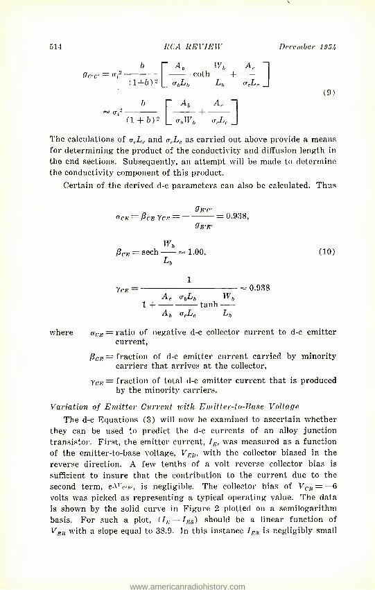
514 KCA REVIEW December 1954
gc,c. = ct,- — ( 1+&)-
b
1 +h)-
Ah
"hL,,
A,,
coth W,,
L„
A,.
A,.
(TrLr. (9)
The calculations of aeL,, and arL,. as carried out above provide a means for determining the product of the conductivity and diffusion length in the end sections. Subsequently, an attempt will be made to determine the conductivity component of this product.
Certain of the derived d-c parameters can also be calculated. Thus
ffrrc 1 ficE ycr, " 0-938,
Wh
Vf/F/
pCK — sech 1.00, CIO)
1 ycr, 0.938
1 +■ ijLf, Wb tanh
Lh T,
where aCE = ratio of negative d-c collector current to d-c emitter current,
f3CE — fraction of d-c emitter current carried by minority carriers that arrives at the collector,
yCB = fraction of total d-c emitter current that is produced by the minority carriers.
Variation of Emitter Current with Emitter-to-Base Voltage The d-c Equations (3) will now be examined to ascertain whether
they can be used to predict the d-c currents of an alloy junction transistor. First, the emitter current, IE, was measured as a function of the emitter-to-base voltage, Fk/j, with the collector biased in the reverse direction. A few tenths of a volt reverse collector bias is sufficient to insure that the contribution to the current due to the second term, e^vc-B-, is negligible. The collector bias of VCK = —6 volts was picked as representing a typical operating value. The data is shown by the solid curve in Figure 2 plotted on a semilogarithm basis. For such a plot, (— IES) should be a linear function of VBn with a slope equal to 38.9. In this instance is negligibly small
www.americanradiohistory.com
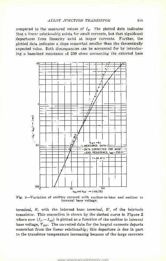
ALLOY JUNCTION TRANSISTOR
compared to the measured values of IE. The plotted data indicates that a linear relationship exists for small currents, but that significant departures from linearity exist at larger currents. Further, the plotted data indicates a slope somewhat smaller than the theoretically expected value. Both discrepancies can be accounted for by introduc- ing a base-lead resistance of 250 ohms connecting the external base
1 A / */ /
/ /
/ / h
L J /
// rf
//
/ f ff
Oi
4/ 'cB = - 6 v — o/
LEAD RESISTANCE, rB8 --250/V.. 24 4e T = C
/
/
/
f
Veb and VEB' —-(VOLTS1
Fig. 2—Variation of emitter current with emitter-to-base and emitter to internal base voltage.
terminal, B, with the internal base terminal, B', of the intrinsic transistor. This correction is shown by the dashed curve in Figure 2 where now (IE — 1ES) is plotted as a function of the emitter to internal base voltage, VEB'. The corrected data for the largest currents departs somewhat from the linear relationship; this departure is due in part to the transistor temperature increasing because of the large currents
www.americanradiohistory.com
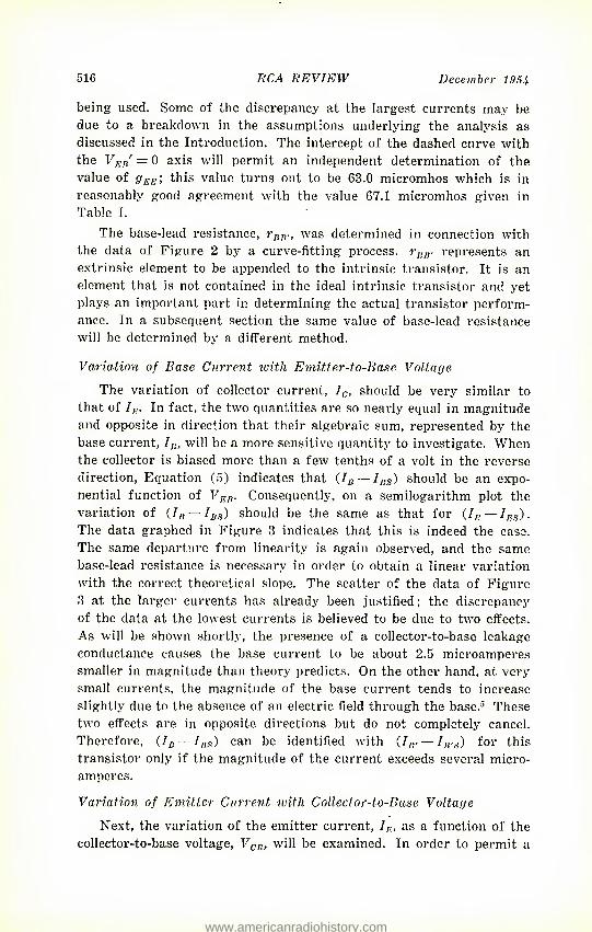
51C RCA REVIEW December 1954
being used. Some of the discrepancy at the largest currents may be due to a breakdown in the assumptions underlying the analysis as discussed in the Introduction. The intercept of the dashed curve with the VEB' = 0 axis will permit an independent determination of the value of gEE; this value turns out to be 63.0 micromhos which is in reasonably good agreement with the value 67.1 micromhos given in Table T.
The base-lead resistance, rnn., was determined in connection with the data of Figure 2 by a curve-fitting process. rnir represents an extrinsic element to be appended to the intrinsic transistor. It is an element that is not contained in the ideal intrinsic transistor and yet plays an important part in determining the actual transistor pei-form- anee. In a subsequent section the same value of base-lead resistance will be determined by a different method.
Variation of Base Current with Emitter-to-Base Voltage
The variation of collector current, Ic, should be very similar to that of I,,. In fact, the two quantities are so nearly equal in magnitude and opposite in direction that their algebraic sum, represented by the base current, will be a more sensitive quantity to investigate. When the collector is biased more than a few tenths of a volt in the reverse direction, Equation (5) indicates that (/,. — 1I!S) should be an expo- nential function of yKB. Consequently, on a semilogarithm plot the variation of (/,; — /g.g) should be the same as that for {IE — 7,,;-s,). The data graphed in Figure 3 indicates that this is indeed the case. The same departure from linearity is again observed, and the same base-lead resistance is necessary in order to obtain a linear variation with the correct theoretical slope. The scatter of the data of Figure 3 at the larger currents has already been justified; the discrepancy of the data at the lowest currents is believed to be due to two effects. As will be shown shortly, the presence of a collector-to-base leakage conductance causes the base current to be about 2.5 microamperes smaller in magnitude than theory predicts. On the other hand, at very small currents, the magnitude of the base current tends to increase slightly due to the absence of an electric field through the base.5 These two effects are in opposite directions but do not completely cancel. Therefore, (Ir. — IIIS) can be identified with (I,,— /«■«) for this transistor only if the magnitude of the current exceeds several micro- amperes.
Variation of Emitter Current with Collector-to-Base Voltage
Next, the variation of the emitter current, IE, as a function of the collector-to-base voltage, V0B, will be examined. In order to permit a
www.americanradiohistory.com
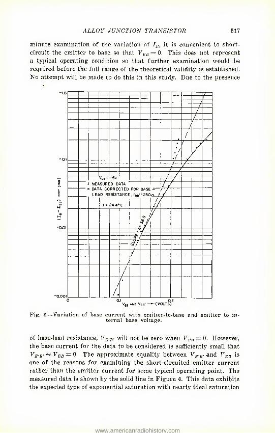
ALLOY JUNCTION TRANSISTOR 517
minute examination of the variation of IE, it is convenient to short- circuit the emitter to base so that VEn = 0. This does not represent a typical operating condition so that further examination would be required before the full range of the theoretical validity is established. No attempt will be made to do this in this study. Due to the presence
/ —
/ / /
/ / t
/
./
/
/ /
< it 01 / / MEASURED DATA / /
0 UAIA LUHHttltU rUK BAbt — / / LEAD RESISTANCE 1rRR'=250yv / /
T = 24 4° C //
.//
O) 03 // *0 !/
//
A / (O / /
r /
/ /
/ / ^
/.
o O.I 0.2 VEB and VEB' —"-(VOLTS)
Pig. 3—Variation of base current with emitter-to-base and emitter to in- ternal base voltage.
of base-lead resistance, will not be zero when VEB = 0. However, the base current for the data to be considered is sufficiently small that VE'B' ** VEB — 0. The approximate equality between F£.B. and VEB is one of the reasons for examining the short-circuited emitter current rather than the emitter current for some typical operating point. The measured data is shown by the solid line in Figure 4. This data exhibits the expected type of exponential saturation with nearly ideal saturation
www.americanradiohistory.com
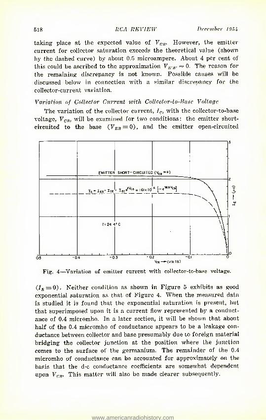
518 RCA REVIEW Deccinber IDSi
taking place at the expected value of VCB. However, the emitter current for collector saturation exceeds the theoretical value (shown by the dashed curve) by about 0.5 microampere. About 4 per cent of this could be ascribed to the approximation 7^- « 0. The reason for the remaining discrepancy is not known. Possible causes will be discussed below in connection with a similar discrepancy for the collector-current variation.
Variation of Collector Current with Collector-to-Base Voltage The variation of the collector current, Ic, with the collector-to-base
voltage, VCI1, will be examined for two conditions: the emitter short- circuited to the base (.VEFl = 0), and the emitter open-circuited
EMITTER SHORT - CIRCUITEC (VEB=O)
IE = IES» I EE ♦ IEC^VcB = I6lx 10 6 [j-e^CB] / /
y
T = 24 4
■ i i i
oc \\ \\ V
Vce-M VOLTS)
Pig. 4—Variation of emitter current with collector-to-base voltage.
(IE=zO). Neither condition as shown in Pigure 5 exhibits as good exponential saturation as that of Pigure 4. When the measured data is studied it is found that the exponential saturation is present, but that superimposed upon it is a current flow represented by a conduct- ance of 0.4 micromho. In a later section, it will be shown that about half of the 0.4 micromho of conductance appears to be a leakage con- ductance between collector and base presumably due to foreign material bridging the collector junction at the position where the junction comes to the surface of the germanium. The remainder of the 0.4 micromho of conductance can be accounted for approximately on the basis that the d-c conductance coefficients are somewhat dependent upon VCB. This matter will also be made clearer subsequently.
www.americanradiohistory.com
ALLOY JUNCTION TRANSISTOR 519
Discussion of Results
When proper allowance is made for the leakage current, the com- puted collector current variation when the emitter is short-circuited checks the measured data very closely as is shown by the dashed curve in Figure 5. When the emitter is open-circuited, the computed-data curve (dashed line) has the same shape as the measured-data curve (solid line), but the measured collector current, when the collector is saturated, is about 0.8 microampere larger than the computed value. This difference is similar to and probably related to the difference noted in connection with Figure 4. It is shown subsequently that the
Vcb —(VOLTS)
d-c conductance coefficients increase as the collector voltage is increased negatively; as noted above, this effect will tend to alter the slope of the characteristics, but the effect is too small to account for a dis- placement of the characteristics. No conclusive explanation for the differences between theory and measurement as noted in Figures 4 and 5 can be advanced at the moment, ft may be significant to note that the open-circuited emitter voltage saturates due to internal con- tact potentials to a value of —76.5 millivolts when the collector is biased into saturation. This value checks reasonably well with the value of —71 millivolts computed for VEI! by setting 1E = 0 in the first of Equations (3). Thus, certain aspects of the theory check closely even though the currents do not check exactly.
www.americanradiohistory.com
520 RCA REVIFAV December l95i
The preceding development has indicated that the d-c character- istics of an alloy junction transistor follow closely the Shockley theory provided a base-lead resistor and a collector-to-base leakage conductor are added to the intrinsic transistor as is shown in Figure 6. The exact placement of gL is not known. For simplicity, it is shown as connected between the collector and the internal base. It is possible however that it should actually be shown connected to some inter- mediate point of rnB'. There may be other series or shunt conductors, but within the scope of the present measurements, they do not appear to be of sufficient importance to be significant. There is some evidence pointing to an emitter-lead impedance, but this element is not in- cluded in this study.
Voltage Variation of Junction and Base Widths
Analytic Formulation As mentioned in the Introduction, when a p-type impurity is
alloyed into an n-type semiconductor, a high-conductivity p-type semi- conductor is formed. The impurity density distribution that results from this alloying process is not known, but from metallurgical con- siderations, it appears likely that the transition from p-type semi- conductor to n-type semiconductor takes place very abruptly as shown in Figure 7(b). It will be assumed here that the transition is infinitely abrupt, as is the case for a metal on a semiconductor, and the conse- quences of the assumption will subsequently be examined to determine whether they are in accord with experimental data. The barrier resulting from a metal-to-semiconductor contact was first studied by Schottky3 and is often identified by his name. Due to differences in
8 For a summary of Schottky's work and complete references, see J. Joffe, "Schottky's Theories of Dry Solid Rectifiers," Electrical Communica- tion, Vol. 22, No. 3, pp. 217-225; 1945. For details of anaylsis, see W. Shockley, op. cit.
www.americanradiohistory.com
ALLOY JUNCTION TRANSISTOR 521
energy levels in the p-type and n-type semiconductors, a contact voltage, exists as shown in Figure 7 (c). The voltage distribution is parabolic in each semiconductor, but penetrates more deeply into the lower conductivity semiconductor which in this case is the n-type material. Accordingly, the distance between points of zero voltage gradient (base width for zero applied voltages) is less than the distance W between points of zero net charge concentration
d) VOLTAGE DISTRIBUTION WITH NORMALLY APPLIED VOLTAGES
Fig. 7—Transistor junction thickness variations.
(metallurgical base width). The emitter and collector junction widths without externally applied voltages are defined respectively as Wr(l
and Wco as shown in Figure 7(c). As depicted here, the portion of the exhaustion region that occurs within the p-type semiconductor is very small and is often neglected. When normal transistor voltages are applied, the junction widths change as shown in Figure 7(d). The emitter is normally biased positively a small amount so that the emitter junction width decreases from its original value. The collector is biased negatively a large amount so that the collector junction width
www.americanradiohistory.com
522 RCA REVIEW December 19 5 U
increases from its original value at the expense of the original base width. To a good approximation, i.e., neglecting the junction widths that occur in the p-type semiconductors,
Wb = W~ (We + Wc). (11)
In accordance with the Schottky theory, the junction widths are given by the expressions
Va, + VE1I' We— [—2 Kc to 4/ , (12 )
11 b
/ ^ + VCI1' Wc =[-2Ke e0 /xn] % \ 7 , (13)
where X',, = relative permittivity (16 for germanium),
e0— permittivity of free space ( X lO^9 farad/meter ) . VSGtt
The constants are those applicable to the base semiconductor. For m.k.s. units, the quantity within the brackets is 10.1 X lO-6. If, as is frequently done, W,. or W,. is in mils (IQ-3 inch), V^+Vc,,. in volts, and ah in mhos/cm, the quantity within the bracket is 0.0398. Oftentimes, the collector-to-base voltage is large enough so that the collector junction width can be computed without knowing the value of V,i„ which is generally not larger than one volt. However, must be known before Wr and Wc can be computed when Vclr is small. This matter will be considered further shortly. At the moment, there will be recorded here for later use the incremental change in base thickness with incremental changes in emitter-to-base and collector-to-base voltage. Thus,
dWb 1
ZVEU. 2
dWb 1
ZVCB. 2
[— 2 Ke <l0 /i„] % ————, (14) V — ff; (.Va + VK,r)
1 [— 2 Ke <l„ ^B]
1^ — — . (15) v' (V(f) VCI1.)
Equations (12), (13), (14), and (15) can be applied to n-p-n tran- sistors by replacing /<,„ with /xp.
www.americanradiohistory.com
ALLOY JUNCTION TRANSISTOR 523
Transition Junction Capacitances The presence of voltages across the junction produces an exhaustion
of majority carriers and, consequently, space-charge layers. This effect gives rise to transition junction capacitances whose values can be simply expressed as
K e co
w,
K
- Ar, (16)
r CTr= f 17)
W.
These equations together with those above for the junction widths
Ctc V - ( n + ) CTc V- (v0 + TW) indicate that and should
-4... Ar
% . In m.k.s. units this constant is be equal to a constant,
■ 2/J.„ 0.701 X 10⁻⁴ farad voltVmeter2 for the (rb = 25 mhos/meter used in the transistor under consideration. Using the collector area as shown
in Figure 1, CTc V—iV^ + VCB) =62.6 X 10⁻¹².
/ 1 \ Measured values of^-^-^ as a function of VCB are shown in
Figure 8. Measurements were made at both 1 and 100 kilocycles. The two sets of data were approximately identical. The data shown in
1 V Figure 8 is in accordance with the theory that ( 1 is linearly re- CT 1 C
lated to Vrn. Actually, there appear to be two linear regions with a rather sharp break occurring at —1.5 volts. This break may be the result of uneven distribution of impurities near the metallurgical junc- tion. The slope of the line for low voltage (scale A) indicates that the constant referred to above has a value of 107 X lO-12 in comparison with the computed value of 62.6 X lO-12. The slope of the line for more negative voltages gives a value of 89 X lO-12 for this same constant.
Determination of Contact Voltage
The value of the contact voltage, Vr!l, can be determined from the
www.americanradiohistory.com
524 RCA REVIEW December 195i
1 \ data shown in Figure 8 by extrapolating to the point where
^T„/z
is zero. When this done (see scale A data), a value of Vtll = — 0.2 volt is determined.
By the application of Shockley's theory for a junction, it can be shown that
In ■ ( 1 + 5 ) 2 /Xj, (7,1 <
ihni "r _ (18)
SCALE A - 2 0 SCALE 8 -20
f = 1 ANC T = 2
IOO kc/s 70C
1 1 1 1 III! -1.5 "15
Fig. 8—Collector transition capacitance variation with voltage.
In this equation, a,, is the conductivity of either the collector or emitter end sections, and iipd is the mobility of holes (majority carriers) in these end sections. Due to the high concentration of impurities in the end sections, the mobility of holes therein may be considerably less than the normal value of //7r Using V,/, = — 0.2 volt as determined above together with values for the other constants in Equation (18),
ad = 520 is obtained. If the normal value of ^ = 0.17 meter2/volt
l-Lpd
sec. is used, (jd = 89 mhos/meter is obtained. These two values appear compatible since the mobility does not decrease appreciably until larger values of conductivity are attained. In the section on d-c char-
www.americanradiohistory.com
ALLOY JUNCTION TRANSISTOR 525
acteristics, it was found that o-./L,, ^ 0.013 mho. Accordingly, an effec- tive diffusion length, L,; = 17 X 10_5 meter, is determined. This length is about an order of magnitude larger than the usually accepted width of the end sections.
The value of ad determined in the preceding paragraph is not in agreement with related data. Thus, according to metallurgical studies and measurements of S. M. Christian,0 o-,, should be in the range of 3,000-30,000 mhos/meter. If ad = 30,000 mhos/meter, then /j.,,,, = 0.02 meterVvolt second, and V,,, = —0.4 volt is to be expected.
From the preceding development it is seen that insofar as the capacitance-voltage is concerned, the alloy-type junction behaves like a Schottky barrier. However, there is some uncertainty about the correct interpretation of the contact voltage in view of the noted ap- parent contradiction in cr,( values.
With the aid of Equations (12) and (13) the transition junction capacitances for zero applied voltage with V^ = — 0.2 can be computed as CT(. — 13.3 micromicrofarads and C}.( = 139 micromicrofarads. When measured by the extrapolated intercept of the scale A curve, CTc is 81.4 micromicrofarads. These transition capacitances are specified here in order to give some idea of the magnitude to be expected. As seen in Figure 8 for CT , these transition capacitances can not be measured directly with certainty due to the fact that minority carrier injection takes place when the voltage is zero, and diffusion capacitances con- tribute to the measured junction capacitances.
Small-Signal Operation
If two terminals, 1 and 2, are picked as the input and output terminals respectively and terminal 3 is common, then the d-c char- acteristics can be expressed generally as I\ = f\{VVXi) and /2 = /2(Fj3, Fas)- The small-signal and low-frequency operation of the transistor can then be expressed in terms of four conductance par-
a/j a/, a/2 a/, ameters,10 gu = , (/i.. = , g-^ = , and gy< — •
ay,, aF,., ay13 ay23
Accordingly, these parameters can be determined from the slopes of the d-c characteristics. If the analytic expressions that have been derived are used for the d-c characteristics, the resulting conductance parameters will be those associated with the intrinsic transistor. In order to obtain the complete parameters, the extrinsic elements must
9 S. M. Christian, RCA Laboratories, Princeton, N. J., personal com- munication.
10 For details see, for instance. Reference (7).
www.americanradiohistory.com
526 RCA REVIEW December 195i
be added in the same manner as considered above for the d-c charac- teristics.
The development of the conductances is carried out most easily for a common-base operation with the emitter as the input terminal, 1, and the collector as the output terminal, 2. This development is car- ried out in the following section. The common-emitter operation is then derived by suitable transformations. The balance of this study is devoted to a detailed check of measured common-emitter parameters with computed values.
For a complete specification of small-signal operation, particularly as regards to frequency, the transistor parameters have both a con- ductive and a susceptive component and are therefore admittance parameters. The approximate susceptive components can be developed rather simply from the conductive component by applying heuristic considerations of the carrier transit times. These considerations are not developed rigorously, but have been found to give results equal to first approximations of more rigorous and more complicated devel- opments.11
In the sections that follow, the equations developed are those for a p-n-p transistor. The corresponding equations for an n-p-n transistor can be obtained by replacing /j,„ and Dp with ixp and Dn respectively. Dn is the diffusion constant of electrons (93 X 10""4 meter'Vsecond for germanium), and Dp is the diffusion constant of holes (44 X 10~4
meterVsecond for germanium).
Common-Base Small-Signal Equivalent Circuit
Conductance Parameters The common-base small-signal conductance parameters for the
intrinsic transistor can be obtained by taking suitable partial deriva- tives of Equations (3), keeping in mind that both the d-c saturation currents and the d-c coefficients are functions via Wh of the terminal voltages as related by Equations (9). Thus, the resulting equations include the effect of base width variation due to emitter-to-base and collector-to-base voltages.12
11 H. Johnson, "Diffusion Reactances of Junction Transistors," IRE- AIEE Transistor Research Conference, Pennsylvania State College, July, 1953. Similar analyses have subsequently been published. See, e.g., J. M. Early, "Design Theory of Junction Transistors," Bell Sys. Tech. Jour., Vol. 32, pp. 1271-1812, November, 19E3; R. L. Pritchard, "Frequency Variations of Junction-Transistor Parameters," Proc. I.R.E., Vol. 42, pp. 786-799, May, 1954; and J. Zawels, "Physical Theory of New Circuit Representation for Junction Transistors," Jour. Appl. Phys., Vol. 25, pp. 976-981, August, 1954.
12 J. M. Early, "Effects of Space-Charge Layer Widening in Junction Transistors," Proc. I.R.E., Vol. 40, pp. 1401-1406, November, 1952.
www.americanradiohistory.com
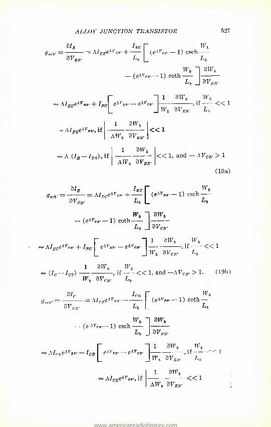
ALLOY JUNCTION TRANSISTOR
3/r IEC
527
dcrh' — — E"■ WEI, Ly,
Wb (eAirBK— 1) csch -
Li,
Wh — (eArcn— 1) coth ■
■'h _l
3ir„
3FR)
Al EEeArji2i' + IR
A/gBeA1 es', if
(>AVeb, — eAVcB' 1 dWb Wh , if « 1 wh ayKJr L,
1 dW
AW h dVmrt' « 1
A (/g »if 1 zwb
AWh VVEB. « 1, and —AVcv > 1
(19a)
3/r ecb'
dVcir L AIFCeAvoB' -\ I (eAVBf — 1) csch ■
Wh
— (eAFcj!— 1) coth W, 1 dWh
] 3yrn.
' A/„;(;eAF CB' + Ir ER' C^CB'
1 dW Wb -.if « 1
Wb dVc,t. Lh
fIc I as) 1 dW,,
Wh ZVrK
IT' if << 1, and —AVCB- > 1. (19b)
dlc
l/reir = = ^CEeAT' w,,,.
Ice P Wh I (exrEH— 1) coth —
Lh i_ Lb
Wh (e AFrB— 1) csch
3TF,
Al( EexrEB— ICE < eb' —
MCEeAVEB', if
dVR
1 3W,, if
TT7,, dVFlff
1 vwb
AW. VVEU. « 1
www.americanradiohistory.com
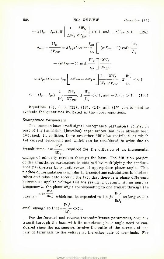
528 RCA REVIEW December 195i
1 1 cWb 1 = A(/t,~ 7(,s), if « 1, and ~AVvl.. > 1. (19c)
I AW, dV^.
Wlt (eA1 £«■ — 1) coth
L„
wb n dw,, — (eAvcB—1) csch
L„ J aVc/r
1 dWh wh if << 1
Wh dVr,r Li,
1 dWtl Wb — do — Ics) , if << 1, and — AFr;,. > 1. (19d)
W,, dVc,,. Lh
Equations (9), (11), (12), (13), (14), and (15) can be used to evaluate the quantities indicated in the above equations.
Susceptance Parameters The common-base small-signal susceptance parameters consist in
part of the transition (junction) capacitances that have already been discussed. In addition, there are other diffusion contributions which are current dependent and which can be considered to arise due to
. . w*2
transit time, t = , required for the diffusion of an incremental mp
change of minority carriers through the base. The diffusion portion of the admittance parameters is obtained by multiplying the conduct- ance parameters by a unit vector of appropriate phase angle. This method of formulation is similar to transit-time calculations in electron tubes and takes into account the fact that there is a phase difference between an applied voltage and the resulting current. At an angular frequency u>, the phase angle corresponding to one transit through the
* • w ■■ ± ju _ Wto- base is e 6D,. which can be expanded to 1 ± jo> as long as o> is
6Dp WV
small enough so that m << 1. GDp
For the forward and reverse transadmittance parameters, only one transit through the base with its associated phase angle need be con- sidered since the parameters involve the ratio of the current at one pair of terminals to the voltage at the other pair of terminals. For
a/c
ff ccb' VVCB.
= .\Iccexv, ICE |
Lh |
AIGfjeAV CB' — 7, CE ^
www.americanradiohistory.com
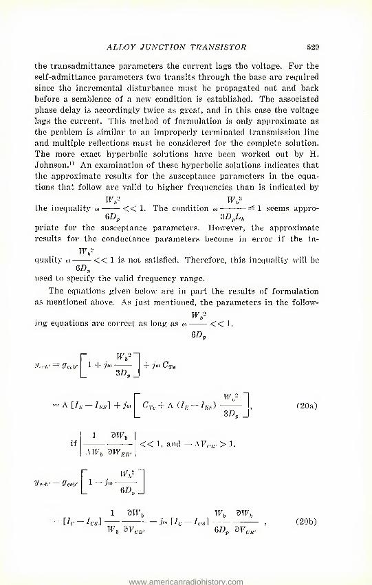
ALLOY JUNCTION TRANSISTOR 529
the transadmittance parameters the current lags the voltage. For the self-admittance parameters two transits through the base are required since the incremental disturbance must be propagated out and back before a semblence of a new condition is established. The associated phase delay is accordingly twice as great, and in this case the voltage lags the current. This method of formulation is only approximate as the problem is similar to an improperly terminated transmission line and multiple reflections must be considered for the complete solution. The more exact hyperbolic solutions have been worked out by H. Johnson.11 An examination of these hyperbolic solutions indicates that the approximate results for the susceptance parameters in the equa- tions that follow are valid to higher frequencies than is indicated by
the inequality <o ■ W wh
6£» << 1. The condition u> - 1 seems appro-
priate for the susceptance parameters. However, the approximate results for the conductance parameters become in error if the in-
quality o) << 1 is not satisfied. Therefore, this inequality will be 6D„
used to specify the valid frequency range. The equations given below are in part the results of formulation
as mentioned above. As just mentioned, the parameters in the follow-
HV mg equations are correct as long as w << 1.
QDn
Vccl 0 ecb' 1 + > wy
3ZV j(j) C rp
A \IE — 7es] + >j WV "I
CTc + A {IPi — lEij) I 3D,,
(20a)
if
Vech' 0 ecb'
1 VWh
AW, dWEn.
WV 1 — jo>
« 1, and — .\Vrn, > 1.
6D„
1 dW Uc-Icsl —._
b Wh dvVB.
wh dWh j'" Uc /«]
&DV Wcu. ('20b)
www.americanradiohistory.com
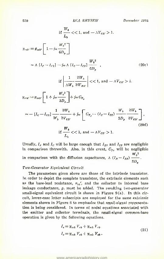
5,'10 RCA REVIEW December I'J.'H
Wb if << 1, and
Lb ■ AyCB. > i.
Vceh' * 9ceh' ' )<i> GDn
A He Irsl i'1' A Uc — ^cs] >r b
6Z>„ I 20c)
if AWh dWf
« 1, and — AVCB' > 1.
[' Vecb' @ccb' I fa*
[Ic-Icsl
HV
3D,.
aw.
vvCB.
+ j<D C'j
+ jo> wh dW,
CT„ (IC Ics) ~ dVr
Wb if << 1, and
Lb
]■ (20d)
■AFr„. >1.
Usually, IE and Ic will be large enough that IES and Ics are negligible in comparison therewith. Also, in this event, Cre will be negligible
MV in comparison with the diffusion capacitance, A (IE — IES) .
3Dp
Two-Generator Equivalent Circuit The parameters given above are those of the intrinsic transistor.
In order to depict the complete transistor, the extrinsic elements such as the base-lead resistance, rh)', and the collector to internal base leakage conductance, g, must be added. The resulting two-generator small-signal equivalent circuit is shown in Figure 9 (a). In this cir- cuit, lower-case letter subscripts are employed for the same extrinsic elements shown in Figure 6 to emphasize that small-signal representa- tion is being considered. In terms of nodal equations associated with the emitter and collector terminals, the small-signal common-base operation is given by the following equations.
Veeb ^eh Verb ^cb*
Ic Vceh Veh Vccb ^cb • (21)
www.americanradiohistory.com
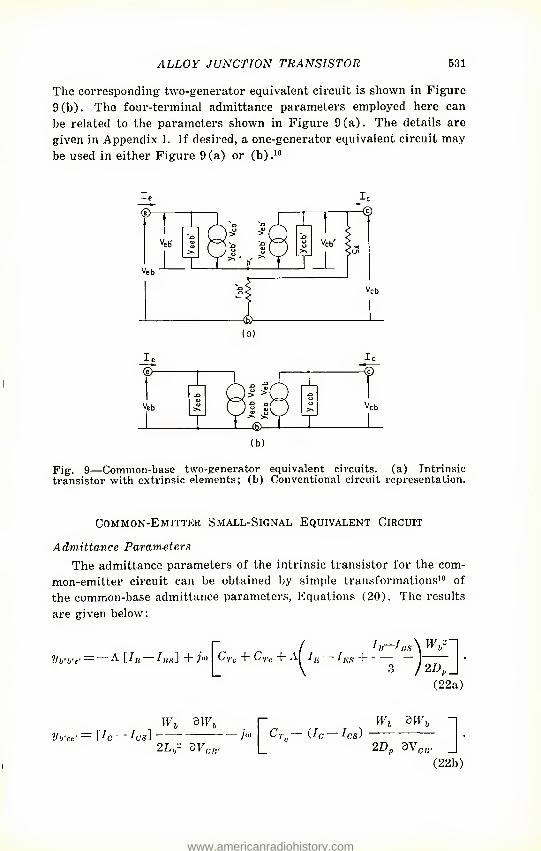
ALLOY JUNCTION TRANSISTOR 531
The corresponding two-generator equivalent circuit is shown in Figure 9(b). The four-terminal admittance parameters employed here can be related to the parameters shown in Figure 9(a). The details are given in Appendix I. If desired, a one-generator equivalent circuit may be used in either Figure 9 (a) or (b) .10
Veb Vcb
pjg. 9—Common-base two-generator equivalent circuits, (a) Intrinsic transistor with extrinsic elements; (b) Conventional circuit representation.
Common-Emitter Small-Signal Equivalent Circuit
Admittance Parameters
The admittance parameters of the intrinsic transistor for the com- mon-emitter circuit can be obtained by simple transformations10 of the common-base admittance parameters, Equations (20). The results are given below:
V b'b'e' ■A [/jj —111S~\ + j'" ^Tc "I" C'i'c + Aj /,, H « 1 US
3 21) p —i (22a)
Wb dWb r Vb'ce' = Uc- - Ics] Crc — Vc — Ics)
zl,;- dVcf:. [_
w,. aw,,
2DP dVC]l. _j (22b)
www.americanradiohistory.com
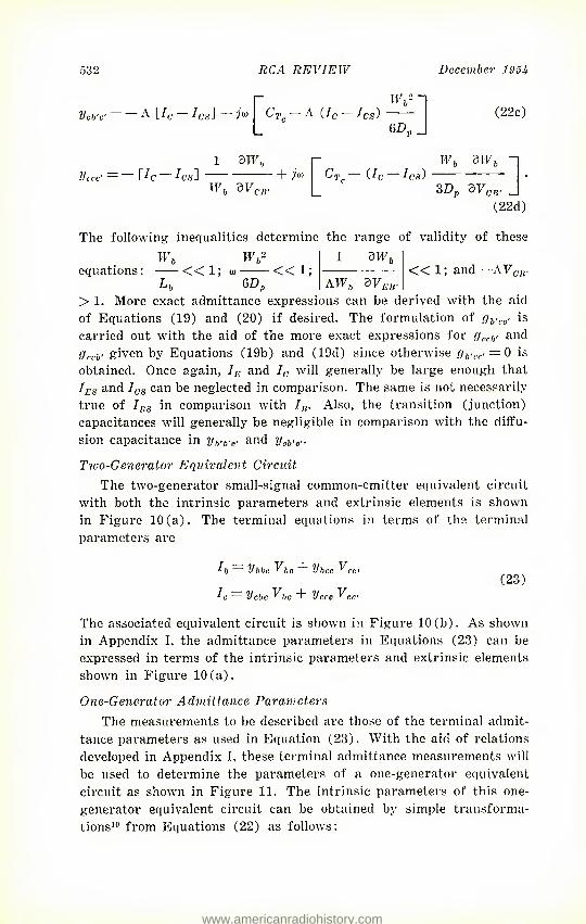
532 RCA REVIEW Deceviber 195U
Vch'e' — ^ /CS] )" Cj' ^ Uc ^cs) W7.2'
GDn
(22c)
1 3W„ l/cce — [/C-^] ^ j"
Wh dVr,r Cr do Ics)
Wb dw,
3Dp dVcrr J (22d)
The following inequalities determine the range of validity of these
Wb equations: << 1;
W,. « 1:
Lb GDp
1 dWb
AW7,, dVEH. « 1; and —A V,;
> 1. More exact admittance expressions can be derived with the aid of Equations (19) and (20) if desired. The formulation of gb.ce. is carried out with the aid of the more exact expressions for gr.aV and gri.b. given by Equations (19b) and (19d) since otherwise gb\.e' = 0 is obtained. Once again, IE and Ic will generally be large enough that IES and Ics can be neglected in comparison. The same is not necessarily true of lyg in comparison with In. Also, the transition (junction) capacitances will generally be negligible in comparison with the diffu- sion capacitance in yb,b'e' and
Two-Generator Equivalent Circuit The two-generator small-signal common-emitter equivalent circuit
with both the intrinsic parameters and extrinsic elements is shown in Figure 10(a). The terminal equations in terms of the terminal parameters are
Vbbe Vbc Vbce
Ic Vche ^"be "i" Vcce ^ce* (23)
The associated equivalent circuit is shown in Figure 10(b). As shown in Appendix I, the admittance parameters in Equations (23) can be expressed in terms of the intrinsic parameters and extrinsic elements shown in Figure 10(a).
One-Generator Admittance Parameters
The measurements to be described are those of the terminal admit- tance parameters as used in Equation (23). With the aid of relations developed in Appendix I, these terminal admittance measurements will be used to determine the parameters of a one-generator equivalent circuit as shown in Figure 11. The intrinsic parameters of this one- generator equivalent circuit can be obtained by simple transforma- tions10 from Equations (22) as follows:
www.americanradiohistory.com
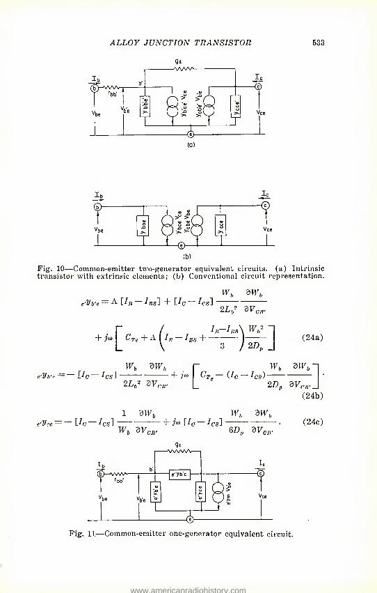
ALLOY JUNCTION TRANSISTOR 533
(a)
-<e> (b)
Fig-. 10—Common-emitter two-generator equivalent circuits, (a) Intrinsic transistor with extrinsic elements; (b) Conventional circuit representation.
sVb'e — A [/B IbsI + He losl w,. dw„
2L,r -dVm'
+ /o) C'Ve + A — IES + Iii Iiis\ "1
3 / 2D„ J (24a)
■■Vb'c— Uc /c8] Wb dw„
2L 2 vv,.,. Joi Ct. UC — Ica)-
iv,. dw,.
e'Vre — Uc 1 3Wb W, dwh
1" }"> Uc — /CS] ' Wb dVCB. GDj, dVCIl.
(24b)
(24c)
Pig'. 11—Common-emitter one-generator equivalent circuit.
www.americanradiohistory.com
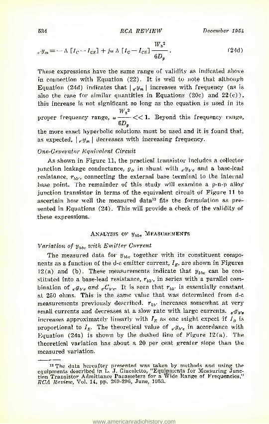
534 RCA REVIEW December 19 Si
WV e'Vm — — ^ [^c — /cS] + -A [/0 — /cS] • (24d)
GDp
These expressions have the same range of validity as indicated above in connection with Equation (22). It is well to note that although Equation (24d) indicates that | e.ym | increases with frequency (as is also the case for similar quantities in Equations (20c) and 22(c)), this increase is not significant so long as the equation is used in its
HV proper frequency range, u> << 1. Beyond this frequency range,
GDP
the more exact hyperbolic solutions must be used and it is found that, as expected, | | decreases with increasing frequency.
One-Generator Equivalent Circuit As shown in Figure 11, the practical transistor includes a collector
junction leakage conductance, gf;, in shunt with ^y^-c aricl a base-lead resistance, rhv, connecting the external base terminal to the internal base point. The remainder of this study will examine a p-n-p alloy junction transistor in terms of the equivalent circuit of Figure 11 to ascertain how well the measured data13 fits the formulation as pre- sented in Equations (24). This will provide a check of the validity of these expressions.
Analysis of ybU Measurements
Variation of yhbe with Emitter Current
The measured data for ybhc together with its constituent compo- nents as a function of the d-c emitter current, IE, are shown in Figures 12(a) and (b). These measurements indicate that ybhe can be con- stituted into a base-lead resistance, rbb', in series with a parallel com- bination of e-fiVe and q'Cb'g. It is seen that rbl, is essentially constant at 250 ohms. This is the same value that was determined from d-c measurements previously described. rbb' increases somewhat at very small currents and decreases at a slow rate with large currents, e-sv, increases approximately linearly with T, as one might expect if I„ is proportional to IF. The theoretical value of C'gb'e in accordance with Equation (24a) is shown by the dashed line of Figure 12(a). The theoretical variation has about a 20 per cent greater slope than the measured variation.
13 The data hereafter presented was taken by methods and using the equipments described in L. J. Giacoletto, "Equipments for Measuring Junc- tion Ti-ansistor Admittance Parameters for a Wide Range of Frequencies," RCA Review, Vol. 14, pp. 269-296, June, 1953.
www.americanradiohistory.com
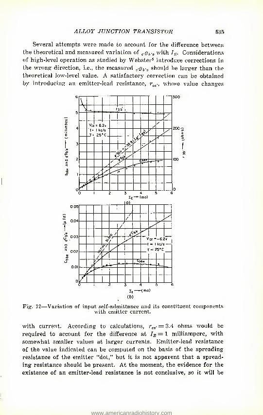
ALLOY JUNCTION TRANSISTOR 535
Several attempts were made to account for the difference between the theoretical and measured variation of with IE. Considerations of high-level operation as studied by Webster5 introduce corrections in the wrong direction, i.e., the measured e'gb'e should be larger than the theoretical low-level value. A satisfactory correction can be obtained by introducing an emitter-lead resistance, rcc., whose value changes
0 01
\ \ 1— r bb'
/ / VCE ="6. 2v / / t = 1 kc/s
?fS0C S & s
s a
■ ,c / /
s—
/ ' y 0
300
3 4 5 IE—Mmo)
/ /
/ / / •c
V V ce --6.2v = 1 kc/s — = 250C /
/ v/
/ ri be •
r / 3 4 5
If—(mo) (b)
Pig. 12—Variation of input self-admittance and its constituent components with emitter current.
with current. According to calculations, = 3.4 ohms would be required to account for the difference at = 1 milliampere, with somewhat smaller values at larger currents. Emitter-lead resistance of the value indicated can be computed on the basis of the spreading resistance of the emitter "dot," but it is not apparent that a spread- ing resistance should be present. At the moment, the evidence for the existence of an emitter-lead resistance is not conclusive, so it will be
www.americanradiohistory.com
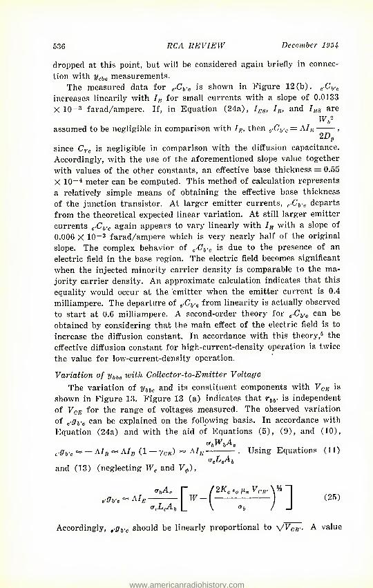
536 RCA REVIEW December 195U
dropped at this point, bat will be considered again briefly in connec- tion with ycie measurements.
The measured data for c.C6.e is shown in Figure 12(b). e'CVe
increases linearily with IE for small currents with a slope of 0.0133 X lO-3 farad/ampere. If, in Equation (24a), IES, In, and IBS are
Wf assumed to be negligible in comparison with IR, then e'Cb'e = AIE ,
2D -,LSp
since CTe is negligible in comparison with the diffusion capacitance. Accordingly, with the use of the aforementioned slope value together with values of the other constants, an effective base thickness = 0.55 X 10—4 meter can be computed. This method of calculation represents a relatively simple means of obtaining the effective base thickness of the junction transistor. At larger emitter currents, e'Cbu. departs from the theoretical expected linear variation. At still larger emitter currents e'Cb,e again appears to vary linearly with IB with a slope of 0.006 X 10⁻³ farad/ampere which is very nearly half of the original slope. The complex behavior of c-CVe is due to the presence of an electric field in the base region. The electric field becomes significant when the injected minority carrier density is comparable to the ma- jority carrier density. An approximate calculation indicates that this equality would occur at the emitter when the emitter current is 0.4 milliampere. The departure of e'Cb'e from linearity is actually observed to start at 0.6 milliampere. A second-order theory for e'CV,, can be obtained by considering that the main effect of the electric field is to increase the diffusion constant. In accordance with this theory,5 the effective diffusion constant for high-current-density operation is twice the value for low-current-density operation.
Variation of ybbe ivith Collector-to-Emitter Voltage The variation of ybbe and its constituent components with VCE is
shown in Figure 13. Figure 13 (a) indicates that rbb. is independent of VCE for the range of voltages measured. The observed variation of e'9b'e can be explained on the following basis. In accordance with Equation (24a) and with the aid of Equations (5), (9), and (10),
<ThWbAc e.gb.e ^ — AI,, ** AIe (1 — yCE) ^ AIe . Using Equations (11)
and (13) (neglecting We and V#),
!, A r P" I €0 H.n Vfn'
iTrLrA i (25)
Accordingly, ..fiVe should be linearly proportional to V^cb- A value
www.americanradiohistory.com
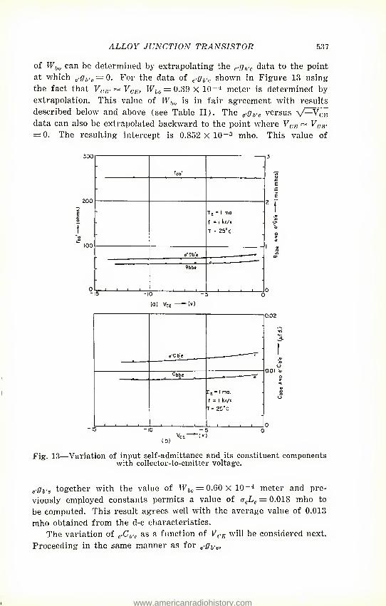
ALLOY JUNCTION TRANSISTOR 537
of Wb0 can be determined by extrapolating the data to the point at which C'gb'e = 0. For the data of ^g^,, shown in Figure 13 using the fact that Vrir^ VeE, = 0.39 X 10⁻⁴ meter is determined by extrapolation. This value of Wh0 is in fair agreement with results described below and above (see Table II). The ^g^e versus V—VCK
data can also be extrapolated backward to the point where Fpg ~ VCB. = 0. The resulting intercept is 0.852 X 10^3 mho. This value of
- rbb' -
-
- IE = 1 mo f = 1 kc/s T = 25° C
e* Ob'e
- 9bbe
la) VcE —-W)
e'Cb'e
■
Cfabe „ —
Ee = 1 mo. f = | kc/s r = 250C
—i—i—.—i— i—. 1 . i i i i__J 0 "15 -10 -5 O
Fig. 13—Variation of input self-admittance and its constituent components with collector-to-emitter voltage.
(,.gh.(. together with the value of IT,,,, = 0.60 X lO"4 meter and pre- viously employed constants permits a value of (jeLe = 0.018 mho to be computed. This result agrees well with the average value of 0.013 mho obtained from the d-c characteristics.
The variation of e.C(/c, as a function of Vr:: will be considered next. Proceeding in the same manner as for e'gb,e,
www.americanradiohistory.com
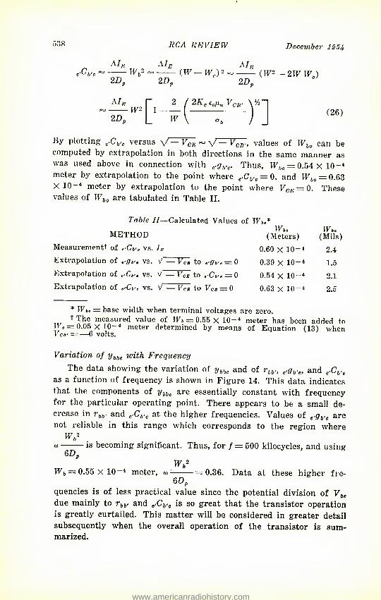
RCA REVIEW December lOSi
A/b - Wc) 2 ^ ( W? — 2W Wr)
2Dn
e'^b'c aie
IIV aIr
— - ^ 2DP 20p
a/b 2 —■—- IF- 1 2D IF
c ^olLn ^ V/r \ ''- (26)
By plotting e.Cb.e versus \/ — VCE - V — yCB., values of Who can be computed by extrapolation in both directions in the same manner as was used above in connection with &gVf.. Thus, Wb0 — 0.54 X 10-,<
meter by extrapolation to the point where ,,,CVe = 0, and Wbo — 0.63 X 10⁻⁴ meter by extrapolation to the point where VCE = 0. These values of Wb0 are tabulated in Table II.
Table II—Calculated Values of Wb.* Wh, Wbo
METHOD (Meters) (Mils) Measurementt of ,'Cb', vs. If. 0.60 x 10⁻⁴ 2.4
Extrapolation of .-sv, vs. V —Vcn to c.fft> = 0 0.39 X 10⁻⁴ 1.5 Extrapolation of ..Cm. vs. V — Vcn to ,'CI,..=0 0.54 x 10⁻⁴ 2.1 Extrapolation of vs. V — Vce to Vci! = 0 0.63 X 10⁻⁴ 2.5
* Wri,0 = base width when terminal voltages are zero, t The measured value of IF,, = 0.55 X lO^4 meter has been added to
lyc = 0.05 X 10⁻⁴ meter determined by means of Equation (13) when v cb' —6 volts.
Variation of ybbe with Frequency
The data showing the variation of ybbe and of rbb., e.gb.e, and e.Cb.e
as a function of frequency is shown in Figure 14. This data indicates that the components of ybbe are essentially constant with frequency for the particular operating point. There appears to be a small de- crease in rbb- and at the higher frequencies. Values of e.gb,e are not reliable in this range which corresponds to the region where
WV m is becoming significant. Thus, for / = 500 kilocycles, and using
6Dp
Wb2
IF;, = 0.55 X 10~4 meter, w =0.36. Data at these higher fre- 6Dp
quencies is of less practical value since the potential division of due mainly to rbb, and is so great that the transistor operation is greatly curtailed. This matter will be considered in greater detail subsequently when the overall operation of the transistor is sum- marized.
www.americanradiohistory.com
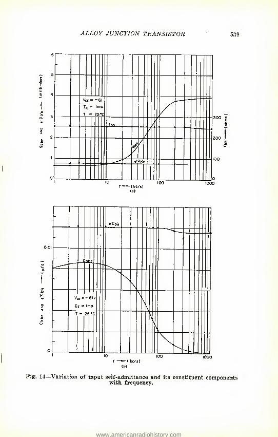
ALLOY JUNCTION TRANSISTOR 539
Vce= -61 IE = Ima. T = 25 0C
rbbl
7
- (kc/s) (a)
.QW.
Vce = — 61 v Ie = Ima T = 250C
cCbe
\
100 f —( kc/s)
(b)
Pig. 14—Variation of input self-admittance and its constituent components with frequency.
www.americanradiohistory.com
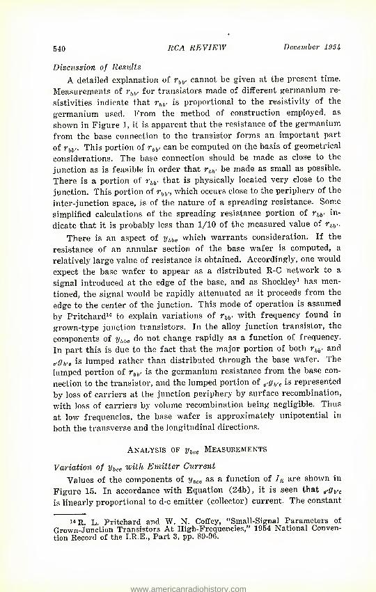
540 RCA REVIEW December 1!)5A
Discussion of Results
A detailed explanation of rbh. cannot be given at the present time. Measurements of rhh, for transistors made of different germanium re- sistivities indicate that rhh. is proportional to the resistivity of the germanium used. From the method of construction employed, as shown in Figure 1, it is apparent that the resistance of the germanium from the base connection to the transistor forms an important part of rbl): This portion of rbb, can be computed on the basis of geometrical considerations. The base connection should be made as close to the junction as is feasible in order that rbV be made as small as possible. There is a portion of that is physically located very close to the junction. This portion of rbb', which occurs close to the periphery of the inter-junction space, is of the nature of a spreading resistance. Some simplified calculations of the spreading resistance portion of rbh. in- dicate that it is probably less than 1/10 of the measured value of rhb..
There is an aspect of yhhe which warrants consideration. If the resistance of an annular section of the base wafer is computed, a relatively large value of resistance is obtained. Accordingly, one would expect the base wafer to appear as a distributed R-C network to a signal introduced at the edge of the base, and as Shockley1 has men- tioned, the signal would be rapidly attenuated as it pi-oceeds from the edge to the center of the junction. This mode of operation is assumed by Pritchard14 to explain variations of rhb. with frequency found in grown-type junction transistors. In the alloy junction transistor, the components of ybbe do not change rapidly as a function of frequency. In part this is due to the fact that the major portion of both rbb, and e.gh.e is lumped rather than distributed through the base wafer. The lumped portion of rbb. is the germanium resistance from the base con- nection to the transistor, and the lumped portion of e.gb.e is represented by loss of carriers at the junction periphery by surface recombination, with loss of carriers by volume recombination being negligible. Thus at low frequencies, the base wafer is approximately unipotential in both the transverse and the longitudinal directions.
Analysis of ybl.c Measurements
Variation of ybce with Emitter Current Values of the components of ybce as a function of IE are shown in
Figure 15. In accordance with Equation (24b), it is seen that e-fiv,, is linearly proportional to d-c emitter (collector) current. The constant
14 R. L. Pritchard and W. N. Coffey, "Small-Signal Parameters of Grown-Junction Transistors At High-Frequencies," 1954 National Conven- tion Record of the I.R.E., Part 3, pp. 89-96.
www.americanradiohistory.com
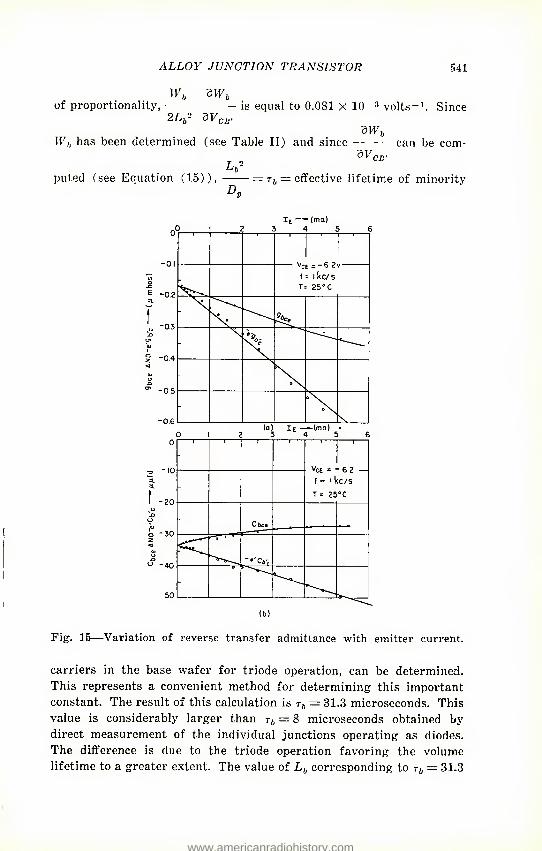
ALLOY JUNCTION TRANSISTOR 541
of proportionality, Wb dW,
2Lb"- 0VCI!.
Wi, has been determined (see Table 11) and since
T 2
— is equal to 0.081 X 10_:i volts-1. Since
dW„ can be com-
puted (see Equation (15)), Dn
zvCB.
Tb = effective lifetime of minority
-06
o
-20
IE —-(mo.) 3 4 5
1 VCE = o c f = ikc/s
T = 25° C
- •v \
0 2 (o) 3 If ——(ma) 4 6
Vrc -
- f = Ikc/s T = 250C
- C bee -r"
r* C6'c
-
(b)
Fig. 15—Variation of reverse transfer admittance with emitter current.
carriers in the base wafer for triode operation, can be determined. This represents a convenient method for determining this important constant. The result of this calculation is t6 = 31.3 microseconds. This value is considerably larger than = 8 microseconds obtained by direct measurement of the individual junctions operating as diodes. The difference is due to the triode operation favoring the volume lifetime to a greater extent. The value of Lb corresponding to r,, = 31.3
www.americanradiohistory.com
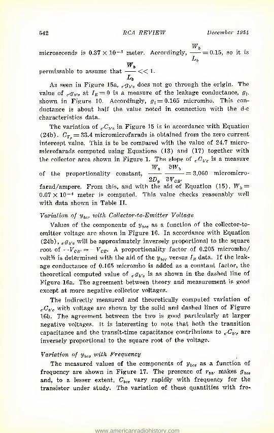
542 RCA REVIEW December 195If
^ . . microseconds is 0.37 X lO-3 meter. Accordingly, =0.15, so it is
Lb Wb
permissable to assume that << 1. Lb
As seen in Figure 15a, does not go through the origin. The value of at /B = 0 is a measure of the leakage conductance, fir,, shown in Figure 10. Accordingly, fif; = 0.165 micromho. This con- ductance is about half the value noted in connection with the d-c characteristics data.
The variation of e'CVc in Figure 15 is in accordance with Equation (24b). CTf = 33.4 micromicrofarads is obtained from the zero current intercept value. This is to be compared with the value of 24.7 micro- microfarads computed using Equations (13) and (17) together with the collector area shown in Figure 1. The slope of e'CVc is a measure
Wt dWh of the proportionality constant, = 3,060 micromicro-
2DV dVCB. farad/ampere. From this, and with the aid of Equation (15), Wb = 0.67 X 10~4 meter is computed. This value checks reasonably well with data shown in Table II.
Variation of yhce with Collector-to-Emitter Voltage
Values of the components of ybce as a function of the collector-to- emitter voltage are shown in Figure 16. In accordance with Equation (24b), e.gb;. will be approximately inversely proportional to the square root of —VCB. «= —VCE. A proportionality factor of 0.205 micromho/ volt% is determined with the aid of the ybce versus IE data. If the leak- age conductance of 0.165 micromho is added as a constant factor, the theoretical computed value of e'gb'C is as shown in the dashed line of Figure 16a. The agreement between theory and measurement is good except at more negative collector voltages.
The indirectly measured and theoretically computed variation of e'Cb'C with voltage are shown by the solid and dashed lines of Figure 16b. The agreement between the two is good particularly at larger negative voltages. It is interesting to note that both the transition capacitance and the transit-time capacitance contribuions to are inversely proportional to the square root of the voltage.
Variation of ybce with Frequency The measured values of the components of ybce as a function of
frequency are shown in Figure 17. The presence of rw makes gbce
and, to a lesser extent, Cbce vary rapidly with frequency for the transistor under study. The variation of these quantities with fre-
www.americanradiohistory.com
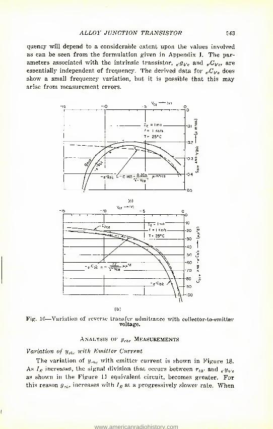
ALLOY JUNCTION TRANSISTOR 543
quency will depend to a considerable extent upon the values involved as can be seen from the formulation given in Appendix I. The par- ameters associated with the intrinsic transistor, e'gb'C and e'Cb'C, are essentially independent of frequency. The derived data for e'Cb'C does show a small frequency variation, but it is possible that this may arise from measurement errors.
(0)
Fig. 16—Vai-iation of reverse transfer admittance with collector-to-emitter voltage.
Analysis of ycbe Measurements
Variation of ycbe with Emitter Current
The variation of ycbe with emitter current is shown in Figure 18. As 1E increases, the signal division that occurs between rbb. and as shown in the Figure 11 equivalent circuit, becomes greater. For this reason gcbe increases with IE at a progressively slower rate. When
www.americanradiohistory.com
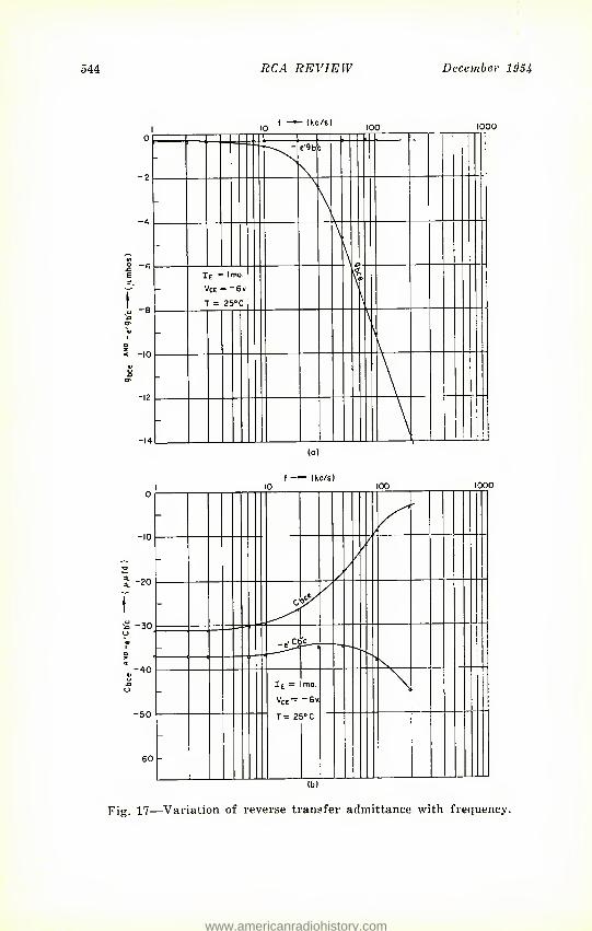
544 RCA REVIEW December l!)5i
l —- lkc/s)
Fig. 17—Variation of reverse transfer admittance with frequency.
www.americanradiohistory.com
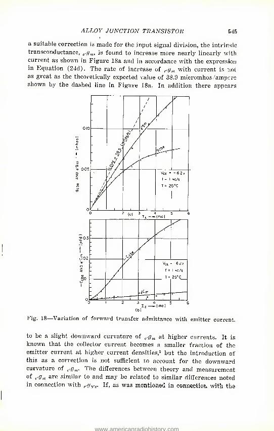
ALLOY JUNCTION TRANSISTOR 545
a suitable correction is made for the input signal division, the intrinsic transconductance, is found to increase more nearly linearly with current as shown in Figure 18a and in accordance with the expression in Equation (24d). The rate of increase of e.gm with current is not as great as the theoretically expected value of 38.9 micromhos, ampere shown by the dashed line in Figure 18a. In addition there appears
Pig. 18—Variation of forward transfer admittance with emitter current.
to be a slight downward curvature of e,gm at higher currents. It is known that the collector current becomes a smaller fraction of the emitter current at higher current densities,5 but the introduction of this as a correction is not sufficient to account for the downward curvature of e.g,n. The differences between theory and measurement of c'9,n are similar to and may be related to similar differences noted in connection with If, as was mentioned la connectioi. with the
www.americanradiohistory.com
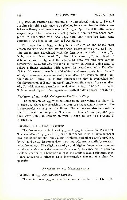
546 RCA REVIEW December 195i
(.■fiVe data, an emitter-lead resistance is introduced, values of 3.9 and 2.2 ohms for this resistance are sufficient to account for the differences between theory and measurements of e/gm at /g = 1 and 3 milliamperes respectively. These values are not greatly different from those com- puted in connection with the g'ffti'e data, and therefore lend some support to the idea of emitter-lead resistance.
The capacitance, Ccbe, is largely a measure of the phase shift associated with the signal division that occurs between rhb. and The capacitance associated with the intrinsic transadmittance, e-COT, is but a small fraction of Ccbe. For this reason, e/Cm is difficult to determine accurately, and the computed data exhibits considerable scattering. Nevertheless, the data as shown in Figure 18b seems to follow a linear variation with current in accordance with Equation (24d). However, there is a disturbing and unaccountable difference of sign between the theoretical formulation of Equation (24d) and the data of Figure 18b. If this difference in sign is overlooked and the formulation of Equation (24d) employed, the slope of the variation of e.Cm with current permits an evaluation of Wb = 0.69 X 10⁻⁴ meter. This value of W,, is in fair agreement with the data shown in Table II.
Variation of ycie with Collector-to-Emitter Voltage
The variation of ycbe with collector-to-emitter voltage is shown in Figure 19. Generally speaking, neither the transconductance nor the transcapacitance vary with voltage. The same can also be said for their intrinsic counterparts. The same differences in and e:Cm
that were noted in connection with Figure 18 are also present in Figure 19.
Variation of ivith Frequency The frequency variation of ycbl, and is shown in Figure 20.
The variation of gcb(. and Crbe with frequency is to a large measure brought about by the input signal division and phase shift produced by rbb' and C'yb-C. In comparison, e-gm and e'Cm are essentially constant with frequency. The slight rise of e.gm at higher frequencies is some- what surprising as a decrease would normally be expected. A possible explanation for this behavior is that the emitter-lead resistance men- tioned above is eliminated as a degenerative element at higher fre- quencies.
Analysis of ycce Measurements
Variation of ycce ivith Emitter Current
The variation of yccil with emitter current is shown in Figure 21.
www.americanradiohistory.com
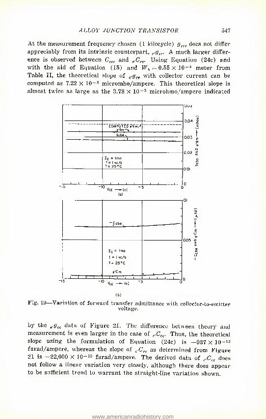
ALLOY JUNCTION TRANSISTOR 547
At the measurement frequency chosen (1 kilocycle) gci.e does not differ appreciably from its intrinsic counterpart, r.gci.. A much larger differ- ence is observed between Ccce and C'Cce. Using Equation (24c) and with the aid of Equation (15) and PF(, = 0.55 X 10^4 meter from Table II, the theoretical slope of e.gce with collector current can be computed as 7.22 X 10~3 micromho/ampere. This theoretical slope is almost twice as large as the 3.78 X 10microhmo/ampere indicated
-
COMPUTED e'9m 9cbe^ v
-
Ie — 1 ma. f = 1 kc/s T = 25 0 C
-
l_. 1 1 1 1 i i i i
(o)
- Ccbc
-
-
I£ = Imo f = 1 kc/s T = 250C
e'Cm
-
.iiii —i - i i i i i i i i
(b) Fig. 19—Variation of forward transfer admittance with collector-to-emitter
voltage.
by the e'gce data of Figure 21. The difference between theory and measurement is even larger in the case of c.Cce. Thus, the theoretical slope using the formulation of Equation (24c) is —937 x 10 -1- farad/ampere, whereas the slope of e.Cce as determined from Figure 21 is —22,000 X 10-12 farad/ampere. The derived data of e.Ccc does not follow a linear variation very closely, although there does appear to be sufficient trend to warrant the straight-line variation shown.
www.americanradiohistory.com
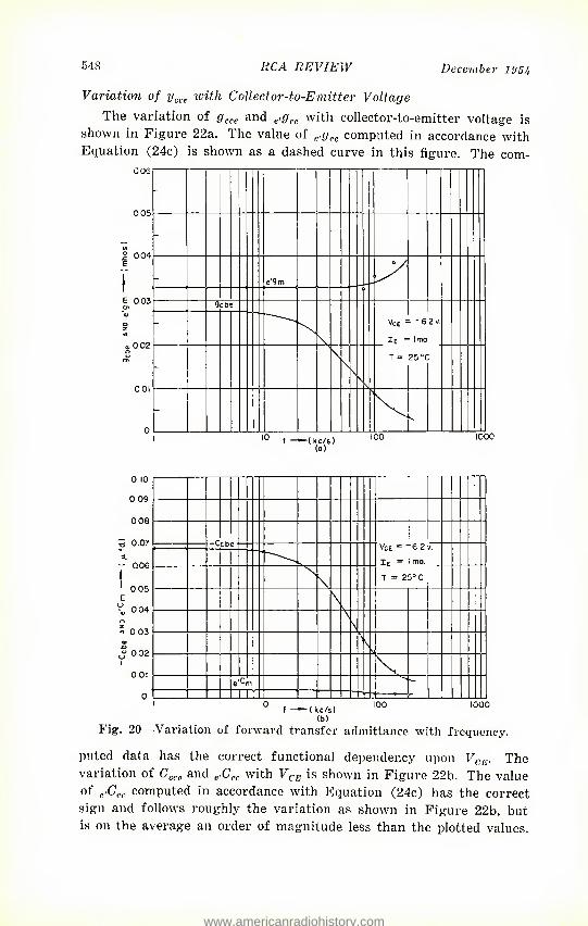
548 RCA REVIEW December 195^
Variation of ycce with Collector-to-Emitter Voltage The variation of gcce and e.gce with collector-to-emitter voltage is
shown in Figure 22a. The value of c.gce computed in accordance with Equation (24c) is shown as a dashed curve in this figure. The com-
006
0 05
| 004 E
£0 03 o> Q z 0,0 02 jO
a»
001
10 f —tkc/s) (a)
-
-
_ e'^m
0 s
q cb
\ - VCE
Ie - 6 2 v Ima
- \ \ \ s N
T = 25 0C
-
0 10 0 09
0 08
5 0 07
4. - 006
' 0 05
^ 004 Q < 0 03
S 0 02 0.01
0 , , , . , tVJU IUWU f —( kc/s)
(b) Fig. 20—Variation of forward transfer admittance with frequency.
puted data has the correct functional dependency upon VCE. The variation of Cccc and e'Ccc with VCE is shown in Figure 22b. The value of computed in accordance with Equation (24c) has the correct sign and follows roughly the variation as shown in Figure 22b, but is on the average an order of magnitude less than the plotted values.
VCE -= Ie =
"6.2 ma
N \ T = 25'C
\ \
s
e'C 1
Tl -
www.americanradiohistory.com
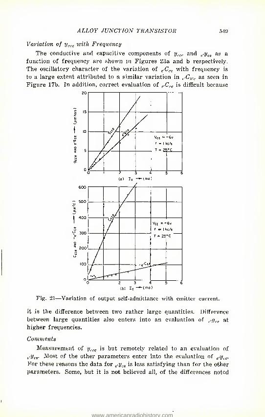
ALLOY JUNCTION TRANSISTOR 549
Variation of ycce with Frequency The conductive and capacitive components of yand e/ycc as a
function of frequency ai-e shown in Figures 23a and b respectively. The oscillatory character of the variation of e.Cce with frequency is to a large extent attributed to a similar variation in e:Ch'r as seen in Figure 17b. In addition, correct evaluation of e'Ccc is difficult because
E jt.
I
0 1 2 3 4 5 6
600
- 500 ■o a. | 400
V 300 o 1, 200
u 100
0 0 1 2 3 4 5 6 (b) Ie
Fig. 21—Variation of output self-admittance with emitter current.
it is the difference between two rather large quantities. Difference between large quantities also enters into an evaluation of at higher frequencies.
Comments
Measurement of ycce is but remotely related to an evaluation of C'yce. Most of the other parameters enter into the evaluation of e.yc(,. For these reasons the data for f:-y,.e is less satisfying than for the other parameters. Some, but it is not believed all, of the differences noted
www.americanradiohistory.com
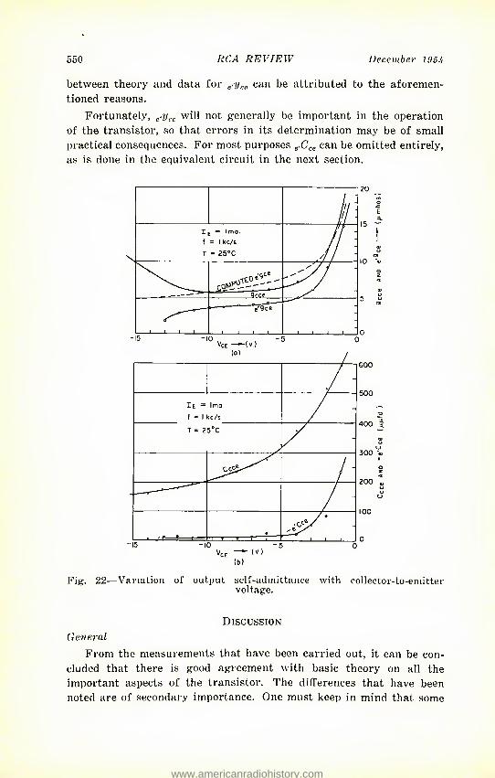
550 RCA REVIEW December l!)5i
between theory and data for e'yee can be attributed to the aforemen- tioned reasons.
Fortunately, C'ycc will not generally be important in the operation of the transistor, so that errors in its determination may be of small practical consequences. For most purposes ^Cce can be omitted entirely, as is done in the equivalent circuit in the next section.
Discussion General
From the measurements that have been carried out, it can be con- cluded that there is good agreement with basic theory on all the important aspects of the transistor. The differences that have been noted are of secondary importance. One must keep in mind that some
www.americanradiohistory.com
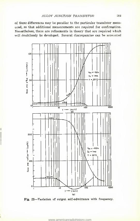
ALLOY JUNCTION TRANSISTOR 551
of these differences may be peculiar to the particular transistor meas- ured, so that additional measurements are required for confirmation. Nevertheless, there are refinements in theory that are required which will doubtlessly be developed. Several discrepancies can be accounted
(b)
Fig. 23—Variation of output self-admittance with frequency.
www.americanradiohistory.com
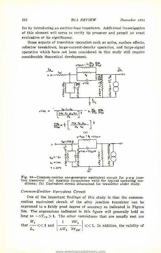
552 RCA REVIEW December lS5i
for by introducing an emitter-lead impedance. Additional investigation of this element will serve to verify its presence and permit an exact evaluation of its significance.
Some aspects of transistor operation such as noise, surface effects, collector breakdown, large-current-density operation, and large-signal operation which have not been considered in this study still require considerable theoretical development.
*' C be Ke € o Ac j~2Ke €o ^.nVcE~| i
8Wb ^ -L [" ZKe 6° Mn S Vca' ^
Wb SWh 2Dp SVca'
"I (0)
e' ® b'c + = 03/iv
Fig. 24—Comnion-emitter one-generator equivalent circuit for p-n-p junc- tion transistor, (a) Analytic formulation valid for typical operating con-
ditions; (b) Equivalent circuit determined for transistor under study.
Common-Emitter Equivalent Circuit One of the important findings of this study is that the common-
emitter equivalent circuit of the alloy junction transistor can be expressed to a fairly good degree of accuracy as indicated in Figure 24a. The expressions indicated in this figure will generally hold as long as —AFcb > 1. The other restrictions that are usually met are
Wh that << 1 and
1
AWh
dw << 1. In addition, the validity of
www.americanradiohistory.com
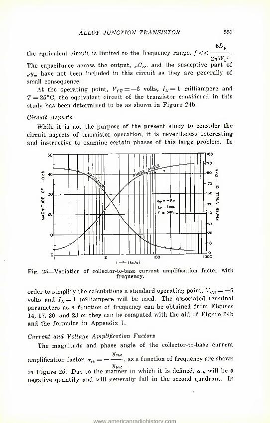
ALLOY JUNCTION TRANSISTOR 553
6Dp
the equivalent circuit is limited to the frequency range, / << . 2TrWh-
The capacitance across the output, c.Cf;„ and the susceptive part of e.ym have not been included in this circuit as they are generally of small consequence.
At the operating point, VCE = —G volts, 7^ = 1 milliampere and T = 250C, the equivalent circuit of the transistor considered in this study has been determined to be as shown in Figure 24b.
Circuit Aspects
While it is not the purpose of the present study to consider the circuit aspects of transistor operation, it is nevertheless interesting and instructive to examine certain phases of this large problem. In
so — —
U 40 0 1 u. ° 30 uj o 3
g 20
10
"| 10 100 IDOO f —— (kc/s)
Fig. 25—Variation of collector-to-base current amplification factor with frequency.
order to simplify the calculations a standard operating point, VCE = —6 volts and IE = 1 milliampere will be used. The associated terminal parameters as a function of frequency can be obtained from Figures 14, 17, 20, and 23 or they can be computed with the aid of Figure 24b and the formulas in Appendix I.
Current and Voltage Amplification Factors
The magnitude and phase angle of the collector-to-base current V che
amplification factor, a,b — , as a function of frequency are shown
in Figure 25. Due to the manner in which it is defined, ach will be a negative quantity and will generally fall in the second quadrant. In
www.americanradiohistory.com
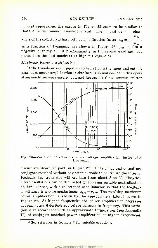
554 RCA REVIEW December 195i
general appearance, the curves in Figure 25 seem to be similar to those of a minimum-phase-shift circuit. The magnitude and phase
Vchc angle of the collector-to-base voltage amplification factor, ixrh = ,
, If cce as a function of frequency are shown in Figure 26. /xcft is also a negative quantity and is predominantly in the second quadrant, but moves into the first quadrant at higher frequencies.
Maximum Power Amplification If the transistor is conjugate-matched at both the input and output,
maximum power amplification is obtained. Calculations1, for this oper- ating condition were carried out, and the results for a common-emitter
Fig. 26—Variation of collector-to-base voltage amplification factor with frequency.
circuit are shown, in part, in Figure 27. If the input and output are conjugate-matched without any attempt made to neutralize the internal feedback, the transistor will oscillate from about 3 to 20 kilocycles. These oscillations can be eliminated by applying suitable neutralization as, for instance, with a collector-to-base inductor so that the feedback admittance is a pure conductance, ybce = gbce. The resulting maximum power amplification is shown by the appropriately labeled curve in Figure 27. At higher frequencies the power amplification decreases approximately 6 decibels per octave increase in frequency. This varia- tion is in accordance with an approximate formulation (see Appendix II) of conjugate-matched power amplification at higher frequencies.
15 See reference in footnote 7 for suitable equations.
www.americanradiohistory.com
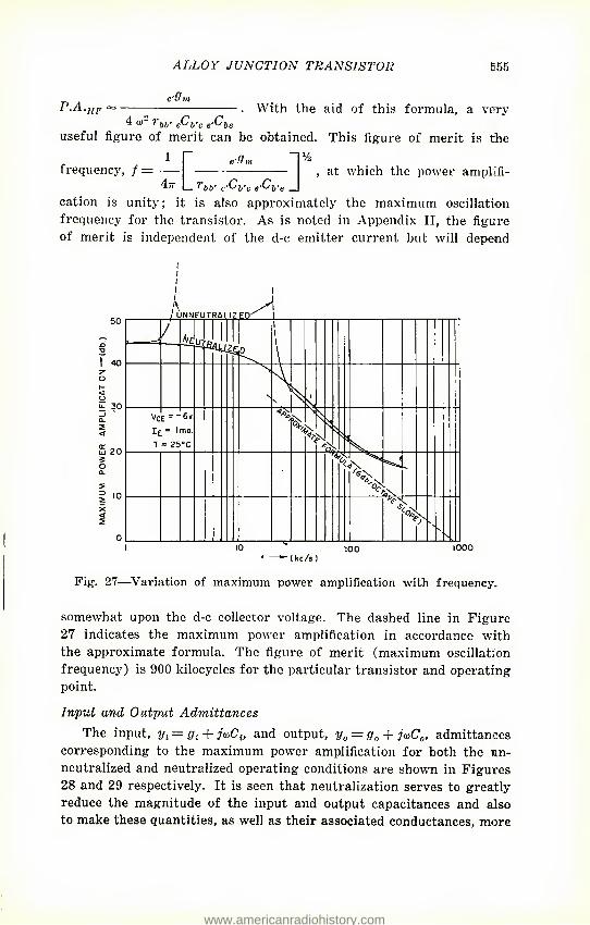
ALLOY JUNCTION TRANSISTOR 555
','0 m . With the aid of this formula, a very
, bh' h'c e'^be useful figure of merit can be obtained. This figure of merit is the
1 frequency, / =
Arr at which the power amplifi-
— 1 bb' c'^-'b'c e'^b'e . cation is unity; it is also approximately the maximum oscillation frequency for the transistor. As is noted in Appendix II, the figui-e of merit is independent of the d-c emitter current but will depend
Pig. 27—Variation of maximum power amplification with frequency.
somewhat upon the d-c collector voltage. The dashed line in Figure 27 indicates the maximum power amplification in accordance with the approximate formula. The figure of merit (maximum oscillation frequency) is 900 kilocycles for the particular transistor and operating point.
Input and Output Admittances The input, 2/4 = 5^ + jwCu and output, y0 = g0 + jwC0, admittances
corresponding to the maximum powTer amplification for both the nn- neutralized and neutralized operating conditions are shown in Figures 28 and 29 respectively. It is seen that neutralization serves to greatly reduce the magnitude of the input and output capacitances and also to make these quantities, as well as their associated conductances, more
www.americanradiohistory.com
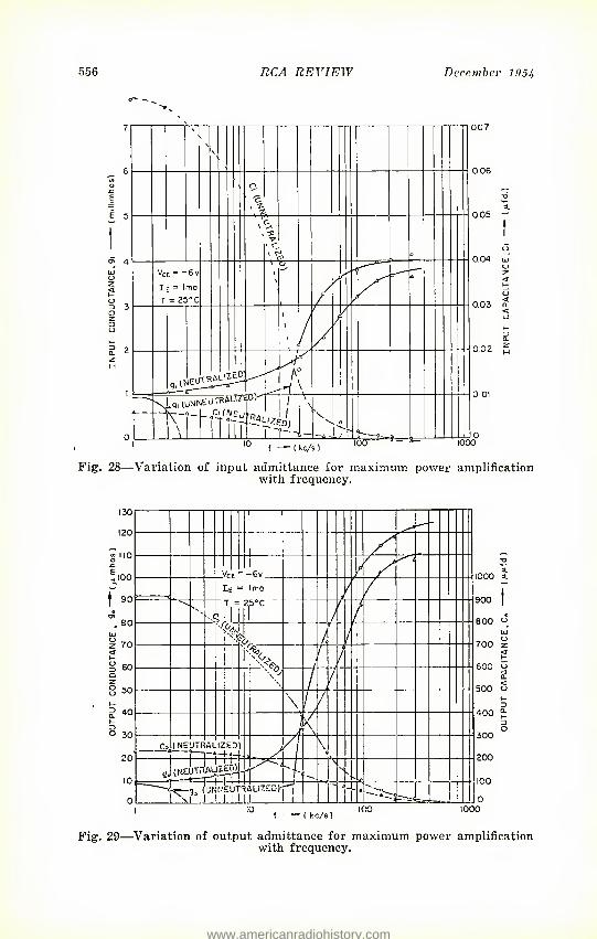
556 RCA REVIEW December 1!)5A
( kc/s) Fig. 28—Variation of input admittance for maximum power amplification
with frequency.
130 120
» no -C i100
f 90 o> , 80
z 70 < 3 60 Q S 50
i 40 o 30
20
10 0
/r = -6v i yS
He = i ma
. < 50C
/ /
I
/
% i
/ \0J
/ 1/
\ / /
J N 0°, ]_Nc jrr — AL -4 .12 — t D
■Y \
Qo 1 1 Ul-r (MEUT^AL^ A \
i\r i i i JTS
11 ALlZCD)-r^
! 1 i IT 1
"O 1000 4.
900 t 800 CJ
in ('GO
600 O n1
S()() o »- _)
400 u. -) c> iOO
200
100 0
-( kc/s)
Fig-. 29—Variation of output admittance for maximum power amplification with frequency.
www.americanradiohistory.com
ALLOY JUNCTION TRANSISTOR 557
nearly constant with frequency. At low frequencies the input capaci- tance for the unneutralized circuit is considerably larger than e.C,/0. This condition is brought about by Miller effect in the same manner as in an electron tube.
As is to be expected, the input admittance at higher frequencies is a pure conductance due to the base-lead resistance. The output admittance at higher frequencies is also a pure conductance due to the current generator activated from a voltage division between e'Cb-c
and e-Ciye as shown in Figure 24. That is, at higher frequencies,
e'^h'c Uo ^ A7C,. When the appropriate values are substituted, this
e'^h'e formulation gives £r() = 119 micromhos which agrees reasonably well with 110-124 micromhos given in Figure 29.
Comments
Although the data given in Figures 27, 28, and 29 is for the particular transistor under study, the results are believed to be gen- erally typical qualitatively and may be considered for other transistors by suitable normalization of the frequency in terms of the figure of merit frequency given above. As was noted previously and as is seen now in Figure 27, the maximum power amplification of the transistor has decreased to a small value when the frequency is large enough so as to invalidate the assumption used in developing the small-signal
QDV parameters, namely that f « .
2itW^
The manner in which the transistor is to be altered in order to obtain single-frequency power amplification at higher frequencies is readily apparent from the preceding development. First, the voltage division between rbb. and must be reduced by decreasing rw
and e'Cbfe. The former can be accomplished by using larger conductivity base material and the latter by making transistors with smaller base thickness. Second, in order to maintain a small output conductance, the feedback capacitance, e/Cyc must be reduced. Neutralization is not successful for this purpose since the internal base point, b', is not accessible. The aforementioned methods of improvement have been employed in the construction of a radio-frequency transistor.16
No systematic study was made of the transistor parameters as a function of temperature. However, temperature enters into the various theoretical formulations, and it is generally believed that the temper-
16 C. W. Mueller and J. I. Pankove, "A P-N-P Tiiode Alloy Junction Transistor for Radio-Frequency Amplification," RCA Review, Vol. 14, pp. 586-598, December, 1953.
www.americanradiohistory.com
558 RCA REVIEW December 195U
ature dependency for the parameters of the intrinsic transistor will be in accordance with these formulations. In addition, rhV will vary in accordance with the resistivity17 of the germanium used. The temperature dependency of gr^ in common with its enigmatic character, does not appear to have a simple behaviour.
Although this study has been restricted to a p-n-p alloy junction transistor made with germanium, the material developed has general applicability to other junction transistors including n-p-n transistors, transistors made from other materials, and transistors made by dif- ferent assembly techniques. It is quite likely, however, that some differences will be noted concerning details of operation.
Conclusions
The general agreement between theory and measurements for the p-n-p alloy junction transistor will make it possible to carry out a large part of the design of a transistor without recourse to the con- struction of devices. The manner in which the transistor operation is dependent upon operating voltage, current, frequency and temper- ature can be predicted within a workable degree of accuracy so that both device and circuit designers can carry out the calculations neces- sary to obtain the answers desired. Many of the factors involved are interrelated so that a compromise will generally be required. The basis for the compromise can be best understood with the aid of calculations based upon the theory. There are several factors concern- ing the transistor which do not appear to be in accordance with theory or for which no theory has as yet been developed. An adequate treat- ment of these factors will serve to complete the picture of the junction transistor.
Appendix I—Formulation of Terminal Parameters
Consider the circuits of Figures 10(a) and 11 with gl lumped in with i/fc-ce- an^ e'Vb'c respectively. The terminal parameters can be formulated by considering a voltage applied to either the input or output terminals and determining the current flowing in either the same or the opposite terminal. The results are
Vb'b'e' e'Vb'e e'2/6'e ybhe = = , (27)
B B
17 P. G. Herkart and J. Kurshan, "Theoretical Resistivity and Hall Coefficient of Impure Germanium Near Room Temperature," RCA Review, Vol. 14, pp. 427-440, September, 1953.
www.americanradiohistory.com
ALLOY JUNCTION TRANSISTOR S59
Vbrc
yfhc '
Vb'ce' e'2/&'c
B B
Vch'e' e'Vm
B B
rbh' l/i'ce' Vcb'e-
(2-8)
( 29)
Vcce y ccc'
where
B ■'Vce e'Vb'c
'jb' c'^6'c- (c'2/m e'Vb'c)
B .30;
1 + rbb- Vli'b'e' — 1 + Tbb' ie'Vb'e + e'Vb'c) (31)
Various other similar relations can be derived either by application of circuit theory or with the aid of suitable transformation equations.10
One set of these relations that may be of value is the terminal param- eters associated with Figure 9(a). Now, gl is assumed to be lumped with yccb..
Veeb ' Vceb' (1 "t- ^bb' Vccb') ^bb' Vecb' Vceb'
B (32)
Verb yecb' (1 ^bb' Vceb') ^*66' Veeb' Vcc
B (33)
Vceb' (1 "l" 1 bb' yeeb') ^bb' Veeb' Verb'
B (34)
Vnh ' Verb' (1 + rhh' yccb') rbb' l/ccb' Vrrh'
B (35)
In these equations, B is the same quantity as in Equation (31), but in terms of the quantities of interest here,
B — 1 + rhb. ( y^. + yceh. + ycch, + yccb.). (36)
For completeness, there is given below the common-collector ter- minal parameters in terms of the common-collector intrinsic transistor parameters and the base-lead resistance. gl is now assumed to be lumped in with y^^,,:
www.americanradiohistory.com
5G0 RCA REVIEW December 195Jf
yb'b'c' ybbc "
B
Vb'ec' ybcc = (38)
B
VrVc' Vebc = (39)
B
^bb' yb'ec' yeb'c' yeec Veec' ' • (40)
B
In these equations, B is the same quantity as in Equations (31) and (36), but in terms of the quantities of interest here,
B = l+rhvyb.h.c: (41)
If the intrinsic and extrinsic parameters in one circuit connection are known and the terminal parameters in another circuit connection are to be determined, generally the easiest method of calculation is to first transform the intrinsic transistor and then calculate the terminal parameters with the aid of one of the sets of equations given above. The alternative method is to first calculate the terminal parameters in the first circuit connection and then transform to the terminal parameters of the second circuit connection.
The inverse problem, that of determining the intrinsic and extrinsic parameters from the terminal parameters is somewhat more involved since there are nine quantities to be determined and only eight equa- tions available from measurements at a single frequency. In general, then, measurements at two or more frequencies will be required. If rbv is determined first, as for example by measurement of yme at two frequencies. Equations (27) through (31) can be readily solved for the other parameters of Figure 11.
c'2//)'c ybbn -^ (1 "f" ^ bb' ybcc) Vhce ' (42)
e'yb'c Vbce ^ • (43)
c'yrc yrcc Mbee ^ ( 1 "I" ' bb' ycbc) • (44)
e'Vm (2/cfae 2/^ce) • (45)
www.americanradiohistory.com
ALLOY JUNCTION TRANSISTOR 5t51
In these equations, B is the same quantity as in Equation (31) but in terms of the quantities of interest here.
1 (46)
1 rbb,yhte
Measurement of yh(.e is necessary in order to permit the separation of e-Vb'c from Usually, however, c/yh'c is sufficiently small in compari- son with e-yye that it can be neglected, and measurment of yhhe can be used for the determination of e-yb'e.
Appendix II — Approximate Formulation op Maximum Power Amplification
Consider the circuit of Figure 24(a) with generator and load con- nected and adjusted for maximum power amplification. At high frequencies, the susceptance of e'Cye is large enough that the input resistance will be approximately rhh.. The input power from a matched generator of open-circuited root-mean-square voltage, Va, will be
(47)
At high frequencies the output admittance is a pure conductance due to the current generator activated from a voltage feedback to e'Cye
through e.Cb.c.
e'^b'c o'Qm (48)
The output power is
P...,
However,
' h'e ' • ^ hb' M h'e
Accordingly, Pc. C'fJ }H
P.A.u,.. = — (50) ^in. 4o)- ? hjj' e'Cfr',. c'Ch'q
c'.9m 1 r/Cye ts'Sin Vb'e~- (49)
4 vCb.0
Vn
This same result can be obtained by introducing suitable approxima- tions in the exact expression for the conjugate-matched power ampli-
www.americanradiohistory.com
562 RCA REVIEW December 1954
fication. When this is done, the range of frequency for which the above equation can be considered valid is determined as
6Dp 1 > 0) > ■
W^hb' e'^b'e
1 The lower limit as represented by will equal or exceed the
^bb' e'^'b'e 1
upper limit if ^ . When this occurs, Equation (50) is no 3A/fl
longer useful.
If desired, Equation (50) can be modified by substituting —A/c
WV for e.gm, and ME for e,Cb.e. Since —I0~1E, the resulting form
2Dp
for the maximum power amplification at high frequencies Is
P.A.HP~ . (51) W b-
2M2 e'Cfr,. DP
WJ The transit time through the base, t = , can also be introduced
6DP
into this equation if desired. The equation above indicates that the maximum power amplifica-
tion at high frequencies should be independent of the emitter current and should increase roughly proportionally with the square root of the collector-to-base voltage due to the voltage dependence of e.Cb.c and tv6.
When Wb is small, e.gce in Figure 24 (a) may not be negligible. In this event, the output conductance. Equation (48), is modified to
b' c (Jo — e'dm + e'Qce > ^52)
e'^b'e
and the power amplification. Equation (50), is modified to
= — — e'^b'c e'9 ce
4r(x)" 1*1)1)' r.'Ch
+ "
www.americanradiohistory.com
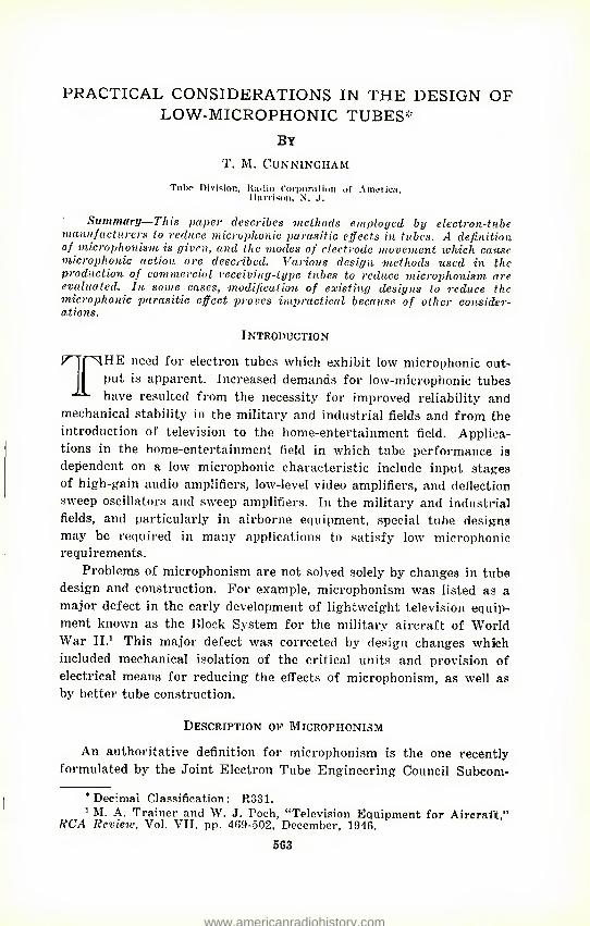
PRACTICAL CONSIDERATIONS IN THE DESIGN OF
LOW-MICROPHONIC TUBES-
By
T. M. Cunningham
Tube Division, Radio Corporation of America, Harrison, N. J.
Summary—This paper describes methods employed by electron-tube manufacturers to reduce microphonic parasitic effects m tubes. A definition of microphonisin is given, and, the modes of electrode movement which cause microphonic action are described. Various design methods used in the production of commercial receiving-type tubes to reduce microphonism are evaluated. In some cases, modification of existing designs to reduce the microphonic parasitic effect proves impractical because of other consider- ations.
Introduction
^ f HE need for electron tube.s which exhibit low microphonic out- ; put is apparent. Increased demands for low-microphonic tubes
have resulted from the necessity for improved reliability and mechanical stability in the military and industrial fields and from the introduction of television to the home-entertainment field. Applica- tions in the home-entertainment field in which tube performance is dependent on a low microphonic characteristic include input stages of high-gain audio amplifiers, low-level video amplifiers, and deflection sweep oscillators and sweep amplifiers. In the military and industrial fields, and particularly in airborne equipment, special tube designs may be required in many applications to satisfy low microphonic requirements.
Problems of microphonism are not solved solely by changes in tube design and construction. For example, microphonism was listed as a major defect in the early development of lightweight television equip- ment known as the Block System for the military aircraft of World War II.1 This major defect was corrected by design changes which included mechanical isolation of the critical units and provision of electrical means for reducing the effects of microphonism, as well as by better tube construction.
Description of Microphonism
An authoritative definition for microphonism is the one recently formulated by the Joint Electron Tube Engineering Council Subcom-
* Decimal Classification: R331. 1 M. A. Trainer and W. J. Poch, "Television Equipment for Aircraft,"
RCA Review, Vol. VII, pp. 469-502, December, 1946.
563
www.americanradiohistory.com
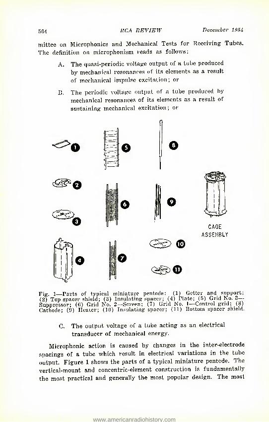
504 RCA REVIEW December 1954
mittee on Microphonics and Mechanical Tests for Receiving Tubes. The definition on microphonism reads as follows;
A. The quasi-periodic voltage output of a tube produced by mechanical resonances of its elements as a result of mechanical impulse excitation; or
B. The periodic voltage output of a tube produced by mechanical resonances of its elements as a result of sustaining mechanical excitation; or
Fig. 1—Parts of typical miniature pentode; (1) Getter and support; (2) Top spacer shield; (3) Insulating spacer; (4) Plate; (5) Grid No. 3— Suppressor; (6) Grid No. 2—Screen; (7) Grid No. 1—Control grid; (8) Cathode; (9) Heater; (10) Insulating spacer; (11) Bottom spacer shield.
C. The output voltage of a tube acting as an electrical
Microphonic action is caused by changes in the inter-electrode spacings of a tube which result in electrical variations in the tube output. Figure 1 shows the parts of a typical miniature pentode. The vertical-mount and concentric-element construction is fundamentally the most practical and generally the most popular design. The most
CAGE ASSEMBLY
transducer of mechanical energy.
www.americanradiohistory.com
LOW-MICROPHONIC TUBES 565
critical electrode spacing is that between the signal grid and the emitting cathode. Microphcnic output can be reduced appreciably by the elimination of sources of "rattle," "knock," or "free-motion" due to loose-fitting parts. However, the electrodes in a vacuum-tube struc- ture are easily excited into vibration by relatively minor vibratory forces acting on the base or the envelope. Since the grid structures are normally composed of wires from one to forty mils in diameter, elastic deflection of the electrodes cannot be entirely prevented no matter how elaborate the design precautions.
The objectionable variations in tube output due to microphoniam occur in the audio-frequency range. There is usually sufficient damping action of the tube electrodes so that only tubes having definitely poor microphonic quality exhibit a characteristic "thump" or "bong" of objectionable amplitude in speaker output when the tube is shock excited. A characteristic "howl" in the speaker known as sustained microphonism may be produced by uncontrolled acoustic feedback from a speaker or by mechanical vibration from an extraneous source, either of which is regenerative in nature.
Testing for Microphonism
When a tube is tested for microphonism, it should be operated in the actual equipment in which it is to be employed, in test equipment which simulates actual application requirements, or in equipment that can be made to correlate with application requirements. The tube under observation must be excited by a mechanical source of vibration or by a mechanical impulse shock. Because receiving tubes are usually applicable to a multiplicity of operations, impulse-shock testing that imparts to the tube structure transient oscillations in the audio-fre- quency spectrum is excellent for evaluating microphonic quality pro- vided it is not necessary to determine a specific resonant frequency.2
The ballistic microphonic test is a practical testing procedure that has given satisfactory results for many years in controlling the micro- phonic level in order to satisfy application requirements. In this test, the tube under test is placed in a resistance-coupled amplifier circuit in which the tube is shock-excited by a tapper, either manual or automatic. The resulting microphonic output is amplified and read on an appropriate meter. The upper limit is set to correlate with applications dependent upon low microphonism.
Figure 2 shows a pendulum-type tapper that standardizes a speci- fied impact which can be correlated with equipment requirements. This
2 A. C. Rockwood and W. R. Ferris, "Micronhonic IniDrovement in Vacuum Tube?," Prnc. Vol. 17, pp. 1621-1632, September, 1929.
www.americanradiohistory.com
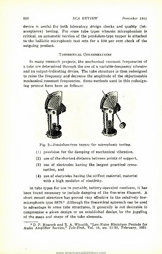
56G RCA REVIEW December 195Jt
device is useful for both laboratory design checks and quality (lot- acceptance) testing. For some tube types wherein microphonism is critical, an automatic version of the pendulum-type tapper is attached to the ballistic microphonic test sets for a 100 per cent check of the outgoing product.
In many research projects, the mechanical resonant frequencies of a tube are determined through the use of a variable-frequency vibrator and an output-indicating device. The tube structure is then redesigned to raise the frequency and decrease the amplitude of the objectionable mechanical resonant frequencies. Some methods used in this redesign- ing process have been as follows:
Pig. 2—Pendulum-type tapper for microphonic testing.
(1) provision for the damping of mechanical vibration,
(2) use of the shortest distance between points of support,
(3) use of electrodes having the largest practical cross- section, and
(4) use of electrodes having the stiffest material, material with a high modulus of elasticity.
In tube types for use in portable, battery-operated receivers, it has been found necessary to include damping of the fine-wire filament. A short mount structure has proved very effective in the relatively low- microphonic type 5879.3 Although the theoretical approach can be used to advantage in some tube structures, it generally is not desirable to compromise a given design or an established design by the juggling of the mass and shape of the tube elements.
3 D. P. Heacock and R. A. Wissolik, "Low-Noise Miniature Pentode for Audio Amplifier Service," Tele-Tech, Vol. 10, pp. 31-33, February, 1951.
Theoretical Considerations
www.americanradiohistory.com
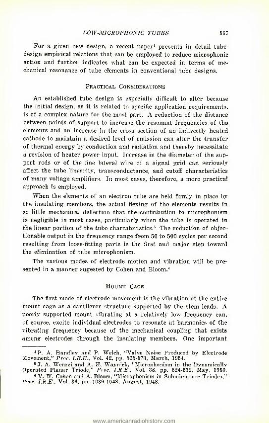
LOW-MICROPHONIC TUBES 567
For a given new design, a recent paper1 presents in detail tube- design empirical relations that can be employed to reduce microphonic action and further indicates what can be expected in terms of me- chanical resonance of tube elements in conventional tube designs.
Practical Considerations
An established tube design is especially difficult to alter because the initial design, as it is related to specific application requirements, is of a complex nature for the most part. A reduction of the distance between points of support to increase the resonant frequencies of tha elements and an increase in the cross section of an indirectly heated cathode to maintain a desired level of emission can alter the transfer of thermal energy by conduction and radiation and thereby necessitate a revision of heater power input. Increase in the diameter of the sup- port rods or of the fine lateral wire of a signal grid can seriously affect the tube linearity, transconductance, and cutoff characteristics of many voltage amplifiers. In most cases, therefore, a more practical approach is employed.
When the elements of an electron tube are held firmly in place by the insulating members, the actual flexing of the elements results in so little mechanical deflection that the contribution to microphonism is negligible in most cases, particularly when the tube is operated in the linear portion of the tube charcateristics.5 The reduction of objec- tionable output in the frequency range from 50 to 500 cycles per second resulting from loose-fitting parts is the first and major step toward the elimination of tube microphonism.
The various modes of electrode motion and vibration will be pre- sented in a manner sugested by Cohen and Bloom.15
Mount Cage
The first mode of electrode movement is the vibration of the entire mount cage as a cantilever structure supported by the stem leads. A poorly suppoi'ted mount vibrating at a relatively low frequency can, of course, excite individual electrodes to resonate at harmonics of the vibrating frequency because of the mechanical coupling that exists among electrodes through the insulating members. One important
4 P. A. Handley and P. Welch, "Valve Noise Produced by Electrode Movement," Proc. T.R.E., Vol. 42, pp. 565-573, March, 1954.
5 J. A. Wenzel and A. H. Wayn:ck, "Microphonism in the Dynamically Operated Planar Triode," Proc. I.R.E., Vol. 38, pp. 524-532, May, 1950.
5 V. W. Cohen and A. Bloom. "Microphonism in Subminiature Triodes," Proc. I.R.E., Vol. 36, pp. 1039-1048, August, 1948.
www.americanradiohistory.com
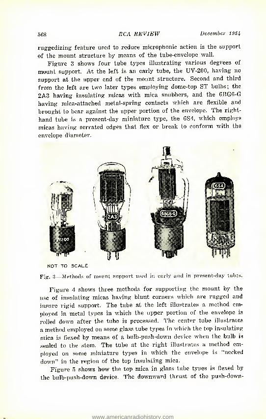
568 RCA REVIEW December 195i
ruggedizing feature used to reduce microphonic action is the support of the mount structure by means of the tube-envelope wall.
Figure 3 shows four tube types illustrating various degrees of mount support. At the left is an early tube, the UV-200, having no support at the upper end of the mount structure. Second and third from the left are two later types employing dome-top ST bulbs; the 2A3 having insulating micas with mica snubbers, and the 6BG6-G having mica-attached metal-spring contacts which are flexible and brought to bear against the upper portion of the envelope. The right- hand tube is a present-day miniature type, the 6S4, which employs micas having serrated edges that flex or break to conform with the envelope diameter.
NOT TO SCALE
Fig-. 3—Methods of mount support used in early and in present-day tubas.
Figure 4 shows three methods for supporting the mount by the use of insulating micas having blunt corners which are rugged and insure rigid support. The tube at the left illustrates a method em- ployed in metal types in which the upper portion of the envelope ia rolled down after the tube is processed. The center tube illustrates a method employed on some glass tube types in which the top insulating mica is flexed by means of a bulb-push-down device when the bulb is sealed to the stem. The tube at the right illustrates a method em- ployed on some miniature types in which the envelope is "necked down" in the region of the top insulating mica.
Figure 5 shows how the top mica in glass tube types is flexed by the bulb-push-down device. The downward thrust of the push-down-
% nm .
www.americanradiohistory.com
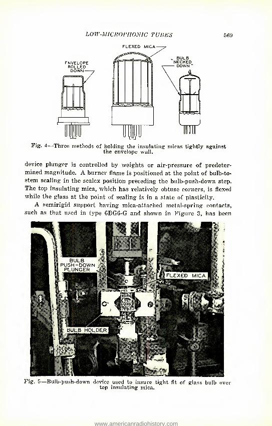
PigT- 4—Three methods of holding the insulating micas tightly against the envelope wall.
device plunger is controlled by weights or air-pressure of predeter- mined magnitude. A burner flame is positioned at the point of bulb-to- stem sealing in the sealex position preceding the bulb-push-down step. The top insulating mica, which has relatively obtuse corners, is flexed while the glass at the point of sealing is in a state of plasticity.
A semirigid support having mica-attached metal-spring contacts, such as that used in type 6BG6-G and shown in Figure 3, has been
LOW-MICROPHONIC TCUES
ENVELOPE ROLLED
DOWN
FLEXED MICA -
, BULB NECKED
DOWN "
Pig. 5—Bulb-push-down device used to insure tight fit of glass bulb over top insulating mica.
www.americanradiohistory.com
570 RCA REVIEW December 195U
found satisfactory for mount cages with relatively large mass. The entire mount absorbs the shock from a mechanical impact. The sup- port has limitations due to wear and enlargement of mica holes from vibrations that approach the resonant frequency of the mount structure.
A rigid mount support is desirable for mount cages having rela- tively small mass that may be subjected to continued mechanical vibra- tion. Because a rigid mount support will readily transmit mechanical impact to the electrodes, it is important that the parts be rigidly fixed in the insulating members.
Rigid mount support by means of the tube envelope wall has been a very effective means for correcting about ten per cent of tubes of several different types that have exhibited uncontrollable microphonic output.
Battery Tube Types
Filamentary types for use in portable, battery-operated receivers are especially prone to sustained microphonic output unless precau- tionary measures are exercised in both design and manufacture. The most prominent and troublesome vibration in these tubes is, of course, the transverse motion of the fine-wire filament.
Figure 6 shows a cutaway drawing illustrating one method em- ployed to increase the resonant frequency and reduce the vibration amplitude of the fine-wire filament.
1. A damper bar having an insulating coating is welded to rela- tively stiu-dy grid side rods. The position of the filament is such that the filament wire bears against the damper bar.
2. A tension arm holds the filament in tension after the filament expands during tube operation.
3. An anchor arm welded to the support-rod leg and to the ten- sion arm is relatively large to damp vibration in the upper region of the filament support.
In this design, the resonant frequency of the filament is shifted by the effective halving of its length and also by the incorporation of a stretching force.
Heater
In Indirectly heated cathode types, the mode of electrode movement of the heater with respect to the cathode is of particular concern, be- cause of variations in heater-cathode capacitance, when tubes are used as oscillators in fi-equency modulation, television, or other short-wave bands. Oscillator circuits in which the cathode is connected across part of the tuned circuit, or in which an alternating voltage exists
www.americanradiohistory.com
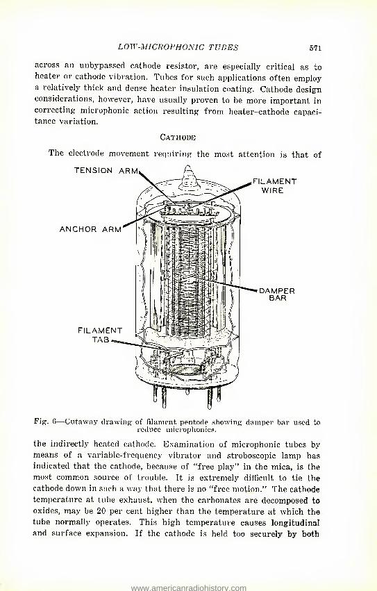
L0W-M1CR0PH0N1C TUBES 571
across an unbypassed cathode resistor, are especially critical as to heater or cathode vibration. Tubes for such applications often employ a relatively thick and dense heater insulation coating. Cathode design considerations, however, have usually proven to be more important in correcting microphonic action resulting from heater-cathode capaci- tance variation.
Cathode
The electrode movement requiring the most attention is that of
Pig. 6—Cutaway drawing of filament pentode showing damper bar used to reduce microphonics.
the indirectly heated cathode. Examination of microphonic tubes by means of a variable-frequency vibrator and stroboscopic lamp has indicated that the cathode, because of "free play" in the mica, is the most common source of trouble. It is extremely difficult to tie the cathode down in such a way that there is no "free motion." The cathode temperature at tube exhaust, when the carbonates are decomposed to oxides, may be 20 per cent higher than the temperature at which the tube normally operates. This high temperature causes longitudinal and surface expansion. If the cathode is held too securely by both
www.americanradiohistory.com
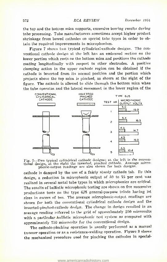
572 RCA REVIEW December 195i
the top and the bottom mica supports, excessive bowing results during tube processing. Tube manufacturers sometimes accept higher product shrinkage from bowed cathodes on special tube types in order to ob- tain the required improvements in microphonism.
Figure 7 shows two typical cylindrical-cathode designs. The con- ventional cathode design at the left has an embossed section on the lower portion which rests on the bottom mica and positions the cathode coating longitudinally with respect to other electrodes. A positive clamping action in the upper cathode region can be obtained if the cathode is inverted from its normal position and the portion which projects above the top mica is pinched, as shown at the right of the figure. The cathode is allowed to slide through the bottom mica when the tube operates and the lateral movement in the lower region of the
CONVENTIONAL CYLINDRICAL
CATHODE INVERTED PINCHED CATHODE
TYPE 6J5 MICROPHONIC
OUTPUT VOLTS 5,0
ISO 1
5.4 •.-.•.••••I 16.5
~n 4.5 "1 14.7
1 4.5
15.0 1
4 5 □
Fig. 7 Two typical cylindrical cathode designs; at the left is the conven- tional design, at the right the inverted, pinched cathode. Average micro-
phonic-output readings are also shown for both designs.
cathode is damped by the use of a fairly sturdy cathode tab. By this design, a reduction in microphonic output of 50 to 75 per cent was realized in several metal tube types in which microphonics are critical. The results of ballistic microphonic testing are shown on five successive productions tests on the type 6J5 general-purpose triode having lot sizes in excess of ten. The average microphonic-output readings are shown for both the conventional cylindrical cathode design and the inverted-pinched-cathode design. The change in design resulted in an average reading referred to the grid of approximately 250 microvolts with a particular ballistic microphonic test system as compared with approximately 750 microvolts for the conventional design.
The cathode-pinching operation is usually performed as a manual tweezer operation or as a resistance-welding operation. Figure 8 shows the mechanized procedure used for pinching the cathodes in special-
www.americanradiohistory.com
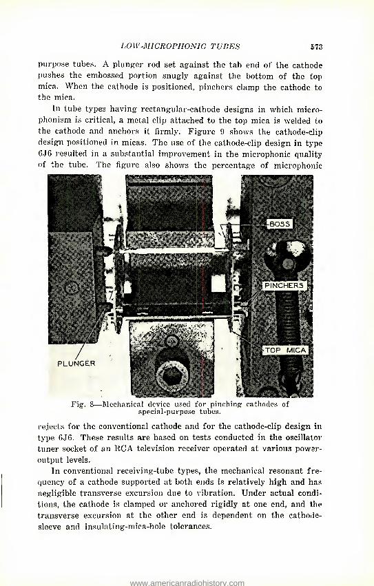
LO W-MlCROPHONIC TUBES 573
purpose tubes. A plunger rod set against the tab end of the cathode pushes the embossed portion snugly against the bottom of the top mica. When the cathode is positioned, pinchers clamp the cathode to the mica.
In tube types having rectangular-cathode designs in which micro- phonism is critical, a metal clip attached to the top mica is welded to the cathode and anchors it firmly. Figure 9 shows the cathode-dip design positioned in micas. The use of the cathode-clip design in type 6J6 resulted in a substantial improvement in the microphonic quality of the tube. The figure also shows the percentage of microphonic
Fig. 8—Mechanical device used for pinching cathodes of special-purpose tubes.
rejects for the conventional cathode and for the cathode-clip design in type 6J6. These results are based on tests conducted in the oscillator tuner socket of an KCA television receiver operated at various power- output levels.
In conventional receiving-tube types, the mechanical resonant fre- quency of a cathode supported at both ends is relatively high and has negligible transverse excursion due to vibration. Under actual condi- tions, the cathode is clamped or anchored rigidly at one end, and the transverse excursion at the other end is dependent on the cathode- sleeve and insulating-mica-hole tolerances.
www.americanradiohistory.com
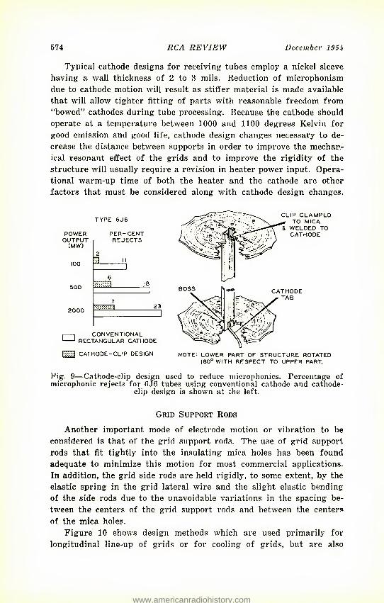
574 RCA REVIEW December 19 5U
Typical cathode designs for receiving tubes employ a nickel sleeve having a wall thickness of 2 to 3 mils. Reduction of microphonism due to cathode motion will result as stiffer material is made available that will allow tighter fitting of parts with reasonable freedom from "bowed" cathodes during tube processing. Because the cathode should operate at a temperature between 1000 and 1100 degrees Kelvin for good emission and good life, cathode design changes necessary to de- crease the distance between supports in order to improve the mechar- ical resonant effect of the grids and to improve the rigidity of the structure will usually require a revision in heater power input. Opera- tional warm-up time of both the heater and the cathode are other factors that must be considered along with cathode design changes.
POWER OUTPUT
(MW) PER-CENT REJECTS
□ CONVENTIONAL RECTANGULAR CATHODE
n CATHODE-CLIP DESIGN NOTE: LOWER PART OF STRUCTURE ROTATED 180° WITH RESPECT TO UPPER PART,
Fig. 9—Cathode-clip design used to reduce microphonics. Percentage of microphonic rejects for 6J6 tubes using conventional cathode and cathode-
clip design is shown at the left.
Grid Support Rods
Another important mode of electrode motion or vibration to be considered is that of the grid support rods. The use of grid support rods that fit tightly into the insulating mica holes has been found adequate to minimize this motion for most commercial applications. In addition, the grid side rods are held rigidly, to some extent, by the elastic spring in the grid lateral wire and the slight elastic bending of the side rods due to the unavoidable variations in the spacing be- tween the centers of the grid support rods and between the centers of the mica holes.
Figure 10 shows design methods which are used primarily for longitudinal line-up of grids or for cooling of grids, but are also
CLIP CLAMPED TO MICA
& WELDED TO CATHODE
www.americanradiohistory.com
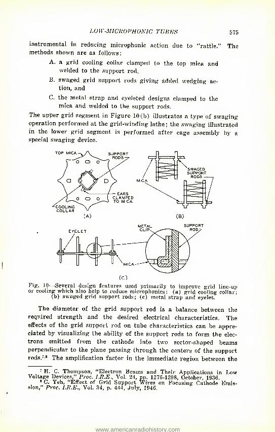
LOW-M1CR0PH0NIC TUBES 575
instrumental in reducing microphonic action due to "rattle." The methods shown are as follows:
A. a grid cooling collar clamped to the top mica and welded to the support rod,
B. swaged grid support rods giving added wedging ac- tion, and
C. the metal strap and eyeleted designs clamped to the mica and welded to the support rods.
The upper grid segment in Figure 10(b) illustrates a type of swaging operation performed at the grid-winding lathe; the swaging illustrated in the lower grid segment is performed after cage assembly by a special swaging device.
METAL SUPPORT
Fig. 10—Several design features used primarily to improve grid line-up or cooling which also help to reduce microphonics: (a) grid cooling collar;
(b) swaged grid support rods; (c) metal strap and eyelet.
The diameter of the grid support rod is a balance between the required strength and the desired electrical characteristics. The effects of the grid support rod on tube characteristics can be appre- ciated by visualizing the ability of the support rods to form the elec- trons emitted from the cathode into two sector-shaped beams perpendicular to the plane passing through the centers of the support rods.7 8 The amplification factor in the immediate region between the
7 H. C. Thompson, "Electron Beams and Their Applications in Low Voltage Devices," Proc. I.R.E., Vol. 24, pp. 1276-1298, October, 1936.
• C. Yeh, "Effect of Grid Support Wires on Focusing Cathode Emis- sion," Proc. I.R.E., Vol. 34, p. 444, July, 1946.
www.americanradiohistory.com
RCA REVIEW December 195 A
grid-No. 1 support rods and the cathode is sufficient so that there is practically no emission from the cathode in that region, through a portion of the negative grid-operating voltage. Increasing the sup- port-rod diameter increases the region from which cathode emission is cut off and, therefore, will adversely affect the linearity of tube char- acteristics in some voltage amplifiers. Receiving tubes having cylin- drical cathodes employ elliptical grids to alleviate this condition. The undesirable effects of the support-rod diameter can be compensated by increasing the distance between the support rods. This change, however, will lower the mechanical resonant frequency of the associated grid lateral wire. In any redesign, it is necessary to consider the mechanical resonance of the support rods and of the lateral wires.
The relative coefficient of rigidity of the material employed for grid support rods is a choice regulated by the application requirements in terms of allowable control-grid emission current through the asso- ciated grid resistor. Applications which require large grid resistors for maximum signal gain necessitate the use of material having high thermal conductivity, such as a chrome-copper alloy, to retard the deleterious effects of grid emission. Relatively stiff material, such as nickel, nickel-plated iron, or copper-clad steel, is normally employed in types designed for applications which are not critical for grid emission. The stiffest support-rod material, in addition to having the highest resonant frequency, also facilitates the assembly of grids in tube manufacture.
Because of the beam-focusing action of the support rods of the control grid, the screen-grid and suppressor-grid support rods are important in the effect on the motion of their respective adjoining grid lateral wires.
Grid Lateral Wires
The movement of grid lateral wires vibrating as rods clamped at each end by the support rods is the mode of vibration most difficult to alter, especially where the grid No. 1 (control grid) is concerned. It is desirable to use large-diameter lateral wire to reduce micro- phonism, but it is often necessary to employ fine grid lateral wire to obtain the desired characteristics.9 For a given medium-mu triode, an increase in the diameter of the grid lateral wire results in deteriora- tion of the plate-current-cutoff and linearity characteristics. In high- transconductance tubes having closely spaced parts, fine grid lateral wire is necessary to minimize the nonuniformity of the electric field
9 m. Benjamin, C. W. Cosgrove, and G. W. Warren, "Modern Reoeivine: Valves: Design and Manufacture," Jour. Inst. Elec. Eng. (Bvit.), Vol. 80, pp. 401-439, April, 1937.
www.americanradiohistory.com
LOW-MICROPHONIC TUBES 577
along the cathode surface due to the grid lateral wires. Fine grid lateral wire size is desirable to provide a high transconductance to plate current ratio in high-transconductance video amplifier tubes having closely spaced parts.1"
An increase in the diameter of the screen-grid (grid-No. 2) lateral wire will usually be judged by the effects on the grid-to-plate capaci- tance and the screen power dissipation. Any increase in the diameter of the suppressor-grid (grid-No. 3) lateral wire should be considered on the basis of its effect on the "knee" of the plate voltage versus plate current characteristic curves.
Like the grid support rod, the grid lateral wire normally consists of the stiffest material possible to facilitate grid winding and tube assembly. Materials commonly used are manganese—nickel alloy, molyb- denum, rhodium-plated molybdenum-tungsten alloy, and gold-plated tungsten wire.
Plate
The vibration of the plate as a stiff diaphragm contributes relatively little to the microphonic output in a vacuum tube, especially in the case of pentodes, because of its physical design and distance from the emitting surface. It has been no problem to wedge the plate structure solidly in the insulating micas. The plate ears are designed to wedge or bite into the micas so that little or no rattle results.
Double Mica
A stop-gap measure used to tighten the tube elements and structure when applications requirements have become more critical for micro- phonism is the double-mica design. One or two extra micas are em- ployed in conjunction with the conventional top and bottom insulating micas. The double-mica design is also employed to anchor small, in- directly heated cathodes when neither the inverted-pinched-cathode design nor the cathode-mica-clip design is satisfactory. The double- mica design has been established as a "ruggedizing" feature for types having short mount heights. In designs where the damping and clamp- ing action of the extra micas have a deleterious effect on tube perform- ance, the cathode hole of the extra mica or micas must be enlarged.
Electrode Spacing
Theoretical considerations have indicated that the first-order effects of mechanical vibration are not important when the structural design
10 J. H. Fremlin, "Calculation of Triode Constants," Electrical Com- mnnicatiov, Vol. 18, pp. 33-49, July, 1939.
www.americanradiohistory.com
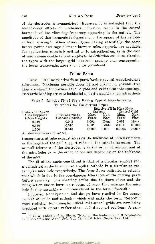
578 RCA REVIEW December 195Jf
of the electrodes is symmetrical. However, it is indicated that the second-order effects of mechanical vibration result in the second harmonic of the vibrating frequency appearing in the output. The amplitude of this harmonic is dependent on the square of the grid-to- cathode spacing.11 When several types having essentially the same heater power and cage distance between mica supports are available for applications especially critical as to microphonism, as in the case of medium-mu double triodes employed in deflection oscillator circuits, the types with the larger grid-to-cathode spacing and, consequently, the lower transconductance should be considered.
Fit of Parts
Table I lists the relative fit of parts having typical manufacturing tolerances. Maximum possible force fit and maximum possible free play are shown for various cage heights and grid-to-cathode spacings. Eccentric bending stresses incidental to part assembly and high cathode
Table I—Relative Fit of Parts Having Typical Manufacturing Tolerances for Commercial Types
Relative Fit in Mica Holes Distance Between Cathode Control Grid
Mica Supports Control-Grid-to- Max. Max. Max. Max. (Cage Height) Cathode Spacing Force Play Force Play
0.340 0.002 0.002 None 0.001 None 0.940 0.010 0.001 0.0015 0.001 0.0005 1.500 0.010 0.0005 0.002 0.0005 0.0015
All dimensions are in inches.
temperatures at tube exhaust increase the likelihood of bowed elements as the length of the grid support rods and the cathode increases. The over-all tolerance of the electrodes is in the order of one mil and of the mica holes is in the order of one mil depending on the thickness of the mica.
The fit of the parts considered is that of a circular support rod, a cylindrical cathode, or a rectangular cathode in a circular or rec- tangular mica hole respectively. The force fit as indicated is actually that which is due to the over-lapping tolerances of the mating parts before assembly. The shearing action due to sharp edges and the filing action due to burrs or rubbing of parts that enlarges the mica hole during assembly is not considered in the term "force-fit."
Improved techniques in tool design have resulted in the manu- facture of grids and cathodes which will make the term "force-fit" more realistic. For example, helical lathe-wound grids are now being produced with smooth rather than notched support rod legs. A cam-
11 V. W. Cohen and A. Bloom, "Note on the Reduction of Microphonics in Triodes," Jour. Appl. ScL, Vol. 18, pp. 847-848, September, 1947.
www.americanradiohistory.com
L0W-M1CR0FH0NIC TUBES 579
acting denotching device lifts the notching wheel between individual grids in the manufacture of a grid strip. Smooth side-rod legs have, of course, been in existence for some time in the ladder-type Kershaw grids. Further, grids are now being produced with "pointed" support- rod ends in order to facilitate assembly. Cathodes are now being produced having ends which are angle-cut, thereby providing a leading edge to further facilitate assembly. These design considerations will insure tighter fitting parts with less possibility of mica hole enlarge- ment at assembly.
Jt has been said that the "hammering action" of an electrode held loosely in a mica hole results in mica fracture and mica-hole enlarge- ment during the life of a tube operating under conditions of severe mechanical vibration. The rate of mica-hole enlargement, resulting from microphonic trouble, is further said to be due to the mass of the tube electrode, the looseness of the fit, and the vibration conditions.12
Some manufacturers employ a triangular or square mica hole for circu- lar support rods or cylindrical cathodes in order to obtain an especially tight fit of the electrodes in commercial types where the mechanical vibration of entertainment equipment is not severe. The rate of mica- hole enlargement is greater for any degree of loose fit, but the "ham- mering action" is reduced by an especially tight fit. This method of obtaining tight-fitting parts and maintaining reasonable manufactur- ing cost may have some merit for a high-production, commercial type, but is avoided for a product demanding unusual reliability during life.
Special-Purpose Tube Types
Vibration tests are useful in determining microphonic quality in the design and development stages of electron-tube work and are also important in controlling the microphonic quality for a specific military or industrial application.
Figure 11 shows the test limits of vibration testing for various special-purpose tube types. The types shown are the "Special Red" type 5692 and commercial type 6SN7-GT, the premium type 6101 and the commercial type 6.16, the premium type 5654 and the commercial type 6AK5. The commercial prototype is shown in each case for com- parison. In the case of special-purpose types, the added design pre- cautions, which include tighter fitting of parts and additional structural support, have proven very effective in reducing microphonic output due to impact shock and vibration. In addition, rigid quality-control procedures are used on parts processing and on parts-assembly opera-
12 A. O'Donnell Roberts. "A Study of Some of the Properties of Materials Affectins- Valve Reliability," Jour. InM. Elec. Eng. (Brit.), Vol. 101, Part III, July, 1954.
www.americanradiohistory.com
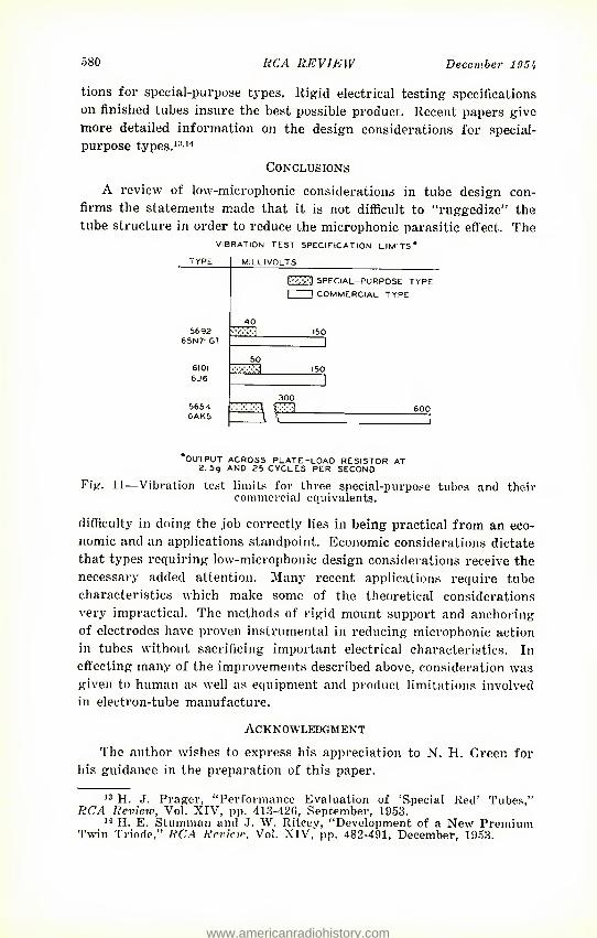
580 RCA REVIEW December 195 Jt
tions for special-purpose types. Rigid electrical testing specifications on finished tubes insure the best possible product. Recent papers give more detailed information on the design considerations for special- purpose types.1314
Conclusions
A review of low-microphonic considerations in tube design con- firms the statements made that it is not difficult to "ruggedize" the tube structure in order to reduce the microphonic parasitic effect. The
VIBRATION TEST SPECIFICATION LIMITS" TYPE MILLIVOLTS
5692 6SN7-GT
6101 6J6
S654 6AKS
I-:i SPECIAL-PURPOSE TYPE " | COMMERCIAL TYPE
"OUTPUT ACROSS PLATE-LOAD RESISTOR AT 2.5g AND 25 CYCLES PER SECOND
Fig. 11—Vibration test limits for three special-purpose tubes and their commercial equivalents.
difficulty in doing the job correctly lies in being practical from an eco- nomic and an applications standpoint. Economic considerations dictate that types requiring low-microphonic design considerations receive the necessary added attention. Many recent applications require tube characteristics which make some of the theoretical considerations very impractical. The methods of rigid mount support and anchoring of electrodes have proven instrumental in reducing microphonic action in tubes without sacrificing important electrical characteristics. In effecting many of the improvements described above, consideration was given to human as well as equipment and product limitations involved in electron-tube manufacture.
Acknowledgment
The author wishes to express his appreciation to N. H. Green for his guidance in the preparation of this paper.
13 H. J. Prager, "Performance Evaluation of 'Special Red' Tubes," RCA Review, Vol. XIV, pp. 413-426, September, 1953.
14 H. E. Stumman and J. W. Ritcey, "Development of a New Premium Twin Triode," RCA Review. Vol. XIV, pp. 482-491, December, 1953.
www.americanradiohistory.com
CABLE EQUALIZATION FOR TELEVISION STUDIO CIRCUITS*
By
Ralph C. Kennedy
Kngineering Department, National Broadcasting Compjiny, Inc., New York, N.
Summary—The procedure for equalizing cable by means of fixed equal- izers is first developed after which the evolution of the variable^ equalizer is presented. The design techniques are augmented by examples detailing the design of both the fixed and variable types of equalizers.
EQUIREMENTS of color-signal transmission place stringent tolerances upon system transmission-versus-frequency and phase-versus-frequency characteristics. Such tolerances have
small purpose if applied only to the active portions of a video circuit. The tolerances must apply equally to cables, phase correctors, and other passive parts of the circuit.
Cable equalization is quite old in the art;1 3 however, the tolerance and bandwidth requirements are new. Additionally, the variable equalizer is relatively new. The problem is divided into two parts, namely, fixed equalization and variable equalization. Some comments which apply to both problems precede the general design study.
The whole problem of cable equalization resolves itself into one of designing a structure having transmission and phase-versus-fre- quency characteristics which are the inverse of the circuit to be equalized. Initially, therefore, the circuit to be equalized must be measured both for transmission and phase.
By transmission characteristic is meant the power loss in decibels versus frequency. The phase characteristic is the variation of the
* Decimal Classification: R117.2 X R143.3. 1 Otto J. Zobel, "Distortion Correction in Electrical Circuits with Con-
stant Resistance Recurrent Networks," Bell Sys. Tech. Jour., Vol. VII, p. 438, July, 1928.
2 H. W. Bode, "Variable Equalizers," Bell Sys. Tech. Jour., Vol. XVII, p. 229, April, 1938.
s H. W. Bode, U. S. Patent 2,096,027, October 19, 1937.
Introduction
Equalization—A Process of Synthesis
581
www.americanradiohistory.com
582 RCA REVIEW December 1956
phase angle as a function of frequency. Obviously, the measurement of transmission and phase must be made with extreme care and ac- curacy since the equalizer must produce a characteristic the inverse of that of the circuit.
Thermocouple power meters are the most desirable units for trans- mission measurements. Any envelope delay measuring equipment having the required degree of accuracy may be used. However, the doubly balanced modulator type is preferable since measurements may be made at desired frequencies.
The particular cable being equalized should be driven by the amplifier normally used with it; however, this is not essential. The termination at the receiving end must be very accurately chosen. The simplest method is to feed the cable with a sweeper and to terminate the cable with a variable resistance whose value is slightly higher than the characteristic impedance of the cable. A 100-ohm poten- tiometer is satisfactory for 75-ohm cable. A diode detector which feeds into an oscilloscope is connected across the input to the cable from the sweeper. Small ripples can be seen in the oscilloscope presen- tation when the resistance value is not equal to the Zn of the line. The potentiometer is adjusted so that no small ripples are present and is then removed and measured on an r-f bridge at about 4 megacycles. This value of resistance should be within ±1 ohm of 75 ohms for W.E. 724 and RG-11U coaxial cables. If it is not equal to this value, it may mean the cable has suffered deformation during installation. In any event the cable cannot be used. The length of cable used for such a test should not exceed 300 feet.
It is obvious that only one termination impedance can be used in studios and master control room. Therefore cables which do not meet the impedance requirement must be rejected, since those cables will have standing waves due to misterminations.
The reason for limiting cable length to 300 feet stems from the fact that a cable's characteristic impedance is a function of frequency. The lower the frequency the higher will be the impedance. At about 4 megacycles the actual impedance of the cable equals the impedance determined by physical dimensions which is called "nominal" or "characteristic" impedance. At that frequency W.E. 724 coaxial video cable has a \Z0\ =75 ohms. However, even for this case the impedance is complex. To terminate any cable over the video band requires that the termination be complex. Equalizer design is exceedingly complex when it is assumed that the source and load impedances are real. To design for complex source and load makes the problem far more com- plicated. To assure that the required source and load are real with
www.americanradiohistory.com
CABLE EQUALIZATION 583
fairly close tolerances, short lengths of cable are used. The effect produced by not terminating in an impedance which is the complex conjugate of the cable impedance is to cause reflections or standing waves on the cable. This causes the cable to present a varying im- pedance to the equalizer. The longer the cable the worse the standing- wave ratio and impedance variation becomes. Thus equalization is applied to cable lengths not exceeding 300 feet. If cables are required to be longer than 300 feet, equalizers may be introduced every 300 feet to provide some isolation between succeeding lengths.
Fixed Equalization
As indicated previously, the design of the equalizer is based on the measured characteristics of the cable. Therefore it is evident that the equalizer can be used only on cables of the same type and length. For a different length of cable the insertion loss must be determined and another equalizer designed. This of course is very time consuming and expensive where many different lengths of cable are in use.
Many concepts which will be useful in the design of variable equalizers can be developed by considering the fixed equalizer design first. We are indebted to Zobel for one of the most useful design procedures.1 As pointed out above, the transmission characteristic in decibels is first measured and plotted as a function of frequency.
It is well at this time to develop a concept for the philosophy of equalization. Essentially a resistive network is first designed whose attenuation is slightly larger than the maximum transmission loss of the circuit to be equalized. Next reactive components are added to the structure so as to cause the attenuation versus frequency to have a characteristic which when added to the characteristic of the circuit to be equalized results in one having constant transmission versus frequency.
When a capacitance is added in parallel to a resistive structure, the impedance of the resulting network is a function of frequency. At sufficiently low frequencies, the network is essentially resistive, the impedance being equal to the d-c resistance; at sufficiently high frequencies, the network is essentially reactive, the impedance ap- proaching zero. The frequency range over which this transition occurs has a spread of about 10 or 20 to 1. The frequency band must, there- fore, be divided so that sections of it are equalized by different equalizers. As an example, a 100-ohm resistor shunted with a 0.1- microfarad condenser has an impedance of 28.5 ohms at 50.3 kilocycles and 94.9 ohms at 5.03 kilocycles. For a 10-megacycle bandwidth two equalizers, one for 100 kilocycles to 1 megacycle and the other from
www.americanradiohistory.com
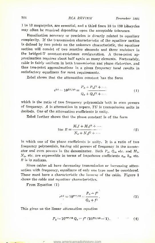
584 HCA REVIEW December 1954
1 to 10 megacycles, are essential, and a third from 10 to 100 kilocycles may often be required depending upon the acceptable tolerance.
Equalization accuracy or precision is directly related to equalizer complexity. If the transmission characteristic of the equalizer section is defined by two points on the unknown characteristic, the equalizer section will consist of two reactive elements and three resistors in the bridged-T constant-resistance configuration. A three-point ap- proximation requires about half again as many elements. Fortunately, cable is fairly uniform in both transmission and phase distortion, and thus two-point approximations in a given frequency band results in satisfactory equalizers for most requirements.
Zobel shows that the attenuation constant has the form
Pn + Pnf^ + ■ • ■ e^A = IQTU/JO = (1)
Qo + Q_'/J + ■ • ■
which is the ratio of two frequency polynomials both in even powers of frequency. A is attenuation in nepers, TU is transmission units in decibels. One of the attenuation coefficients is unity.
Zobel further shows that the phase constant is of the form
Mi/ + M,/3 + • • • tan B (2)
Nn + N,P + ■■■
in which one of the phase coefficients is unity. It is a ratio of two frequency polynomials, having odd powers of frequency in the numer- ator and even powers in the denominator. Both P0, Q0, etc. and Mu
N0, etc. are expressible in terms of impedance coefficients a,,, bn, etc. B is in radians.
Since cables all have decreasing transmission or increasing atten- uation with frequency, equalizers of only one type need be considered. These must have a characteristic the inverse of the cable. Figure 1 shows the cable and equalizer characteristics.
From Equation (1)
p. + r- e2A ~ l07,"/i() = . C3) Qu + P
This gives us the linear attenuation equation
PQ — IO^/K) Q0 = p (10™/io — l) (A)
www.americanradiohistory.com
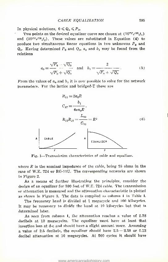
CABLE EQUALIZATION 585
In physical solutions, 0 < Q0 < P0. Two points on the desired equalizer curve are chosen at (lO7,17!/10,/!)
and (10I't72/10,/2). These values are substituted in Equation (4) to produce two simultaneous linear equations in two unknowns P0 and Qn. Having determined P0 and Q0, au and b1 may be found from the relations
VFn - ^ 2 Uq — and bj = . (5)
V-Po + V Qn V-Po + V Qo
From the values of a0 and b, it is now possible to solve for the network parameters. For the lattice and bridged-T these are
Bj l =2a0R
Loo = —— — E- C6)
C12
Fig. 1—Transmission characteristics of cable and equalizer.
where is the nominal impedance of the cable, being 75 ohms in the case of W.E. 724 or RG-HU. The corresponding networks are shown in Figure 2.
As a means of further illustrating the principles, consider the design of an equalizer for 300 feet of W.E. 724 cable. The transmission or attenuation is measured and the attenuation characteristic is plotted as shown in Figure 3. The data is compiled as column 1 in Table I.
The frequency band is divided at 1 megacycle and 100 kilocycles. It may be necessary to divide the band at 10 kilocycles but that is determined later.
As seen from column 1, the attenuation reaches a value of 2.38 decibels at 10 megacycles. The equalizer must have at least that insertion loss at d-c and should have a slight amount more. Assuming a value of 2.5 decibels, the equalizer should have 2.5 — 2.38 or 0.12 decibel attenuation at 10 megacycles. At 500 cycles it should have
www.americanradiohistory.com
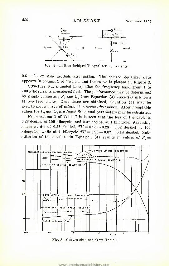
586 RCA REVIEW December 105i
2.5 .05 or 2.45 decibels attenuation. The desired equalizer data appears in column 2 of Table I and the curve is plotted in Figure 3.
Structure #1, intended to equalize the frequency band from 1 to 100 kilocycles, is considered first. The performance may be determined by simply computing P0 and Q0 from Equation (4) since TU is known at two frequencies. Once these are obtained, Equation (4) may be used to plot a curve of attenuation versus frequency. After acceptable values for P0 and Q,, are found the actual parameters may be calculated.
From column 1 of Table I it is seen that the loss of the cable is 0.23 decibel at 100 kilocycles and 0.07 decibel at 1 kilocycle. Assuming a loss at d-c of 0.25 decibel, Tf/= 0.25 — 0.23 = 0.02 decibel at 100 kilocycles, while at 1 kilocycle TU = 0.25 — 0.07 = 0.18 decibel. Sub- stitution of these values in Equation (4) results in values of P0 =
Fig. 3—Curves obtained from Table I.
www.americanradiohistory.com
CABLE EQUALIZATION £87
1274.8 X 106 and Q0 = 1223 X 106. Using these in Equation (4) ailows the computation of loss versus frequency shown in column 3 which is the loss characteristic of structure #1. Column 4 is the sum of cable and equalizer #1 losses which are also plotted on Figure 3.
The design of equalizer #2, covering the frequency band from 100 kilocycles to 1 megacycle proceeds from the data of column 4. Since the new characteristic is fairly constant to 200 kilocycles, this value
Table I
(D P4 O) -
oj o 2 O o;
O CO SH o C^J LO O CO t- CO o T-H
rH Q at o C+t: o 'o 'o 'o O
o C3 ^
CJ +
o S ^
O +
O C3 ^ 2 • —
O +
O 1
•2 T3 ^ t? a a; 2 W N
O +
1 1—1 Sf CD 00 C a; ? ^ Oi lO -t-> cr 'o CJ
^ cr 'o £ c 'o o 'o eg <; w O CH O O <! oW O
Fre- quency (mega cycles) Coll Col 2 ColS Col i
decibels Col 5 Col 6 Col ColS Col 9 Col 10 Colll
.0005
.001
.002
.004
.007
.010
.02
.04
.06
.10
.20
.50 1 2 3 4 5 6 7 8 9
10
.048
.066
.090
.119
.142
.155
.172
.186
.199
.230
.309
.477
.693 1.008 1.254 1.461 1.644 1.809 1.968 2.112 2.247 2.379
2.452 2.434 2.410 2.381 2.358 2.345 2.328 2.314 2.301 2.270 2.191 2.023 1.807 1.492 1.246 1.039
.856
.691
.532
.388
.253
.121
.180
.180
.180
.178
.173
.167
.136
.079
.046
.024
.005 0 0 0 0 0 0 0 0 0 0 0
.228
.250
.270
.297
.315
.322
.308
.265
.245
.254
.314
.477
.693 1.008 1.254 1.461 1.644 1.809 1.968 2.112 2.247 2.379
.513
.513
.513 .513 .513 .513 .512 .510 .505 .491 .434 .240 .093 .027 .012 .007 0 0 0 0 0 0
.741
.763
.783 .810 .828 .835 .820 .775 .750 .745 .748 .717 .786
1.035 1.266 1.468 1.644 1.809 1.968 2.112 2.247 2.379
1.814 1.814 1.814 1.814 1.814 1.814 1.814 1.813 1.813 1.813 1.810 1.788 1.714 1.473 1.193
.943
.744
.591
.475
.388
.321 .269
2.555 2.577 2.597 2.624 2.642 2.649 2.634 2.588 2.563 2.558 2.558 2.505 2.500 2.508 2.459 2.411 2.388 2.400 2.443 2.500 2.568 2.648
2.375 2.397 2.417 2.446 2.469 2.482 2.498 2.509 2.517 2.534 2.553 2.505 2.500 2.508 2.459 2.411 2.388 2.400 2.443 2.500 2.568 2.648
.113
.113
.112
.112
.111
.109
.098
.071
.048
.024
.007 0 0 0 0 0 0 0 0 0 0 0
2.488 2.510 2.529 2.558 2.580 2.591 2.596 2.580 2.565 2.558 2.560 2.505 2.500 2.508 2.459 2.411 2.388 2.400 2.443 2.500 2.568 2.648
can be the lower bound and 1 megacycle the upper bound. Column 4 shows the loss to be 0.69 decibel at 1 megacycle and 0.31 decibel at 200 kilocycles. If the d-c insertion loss is 0.50 decibel, then this plus the attenuation of equalizer #1 is 0.75 decibel. Then T{7 = 0.75— 0.31 = 0.44 decibel at 200 kilocycles and 0.75 — 0.69 = 0.06 decibel at 1 megacycle. Pn is 0.234 X lO12 and Q,, is 0.208 X 10¹². Column 5 is the loss characteristic for the structure and column 6 is the sum of the cable, equalizer #1 and equalizer #2 ("See Figure 3).
www.americanradiohistory.com
588 RCA REVIEW December 1954
Equalizer #3 is designed from the data in column 6. Initially it was decided that the total insertion loss for complete equalization of the cable would be 2.5 decibels. The value of TU for equalizer #3 at 1 megacycle is 2.5 — 0.79 = 1.71 decibels and at 8 megacycles is 2.5 — 2.112 = 0.388 decibel. P0 then is 21.37 X 10¹² and Qy = 14.08 X 10¹². The characteristic of the equalizer is tabulated in column 7 while column 8 is the resultant characteristic for the cable and the three equalizers. These values ai-e also plotted in Figure 3.
The attenuation of the equalized circuit is constant to within ±.13 decibel or ±1.5 per cent. No tolerance was initially stipulated, so it is possible that this deviation is acceptable. If a closer tolerance is required, it is obtained in the following manner. It is seen that the largest deviations occur between 10 and 20 kilocycles and between 5 and 10 megacycles. The former region is controlled by equalizer #1 and the latter by equalizer #3.
If the characteristics of equalizer #1 as given in column 3 are subtracted from column 8, the result is the sum of equalizers #2 and #3 and the cable and is found in column 9. Equalizer #1 can then be redesigned with TC/= 2.558 — 2.446 = 0.112 decibel at 4 kilocycles and TU = 2.558 — 2.534 = 0.024 decibel at 100 kilocycles, from which P„ = 2741.8 X 10° and Q(l = 2671.6 X 101
The new characteristic for equalizer #1 is given in column 10, and the sum of the three plus the cable in column 11. The curves are all plotted on Figure 3. It is seen that the variation between 10 and 20 kilocycles has been reduced. By a similar procedure the varia- tion between 5 and 10 megacycles may be reduced, though it is possible that a fourth structure might be required. Similarly, an additional structure may be required to control the 500-cycle variation. Clearly the closer the tolerance the more complex the complete equalizer becomes.
Assuming that the final characteristic shown in Figure 3 is accept- able, it is possible to proceed to the design of the physical structures. Equations (5) and (6) are used to compute the values of a0, hu and the elements.
Using the values of P0 and Q0 for each of the equalizers results in the following values for each structure:
h, Cn Ru L.™
Equalizer #1 0.00649
19.22 X 10-"
Equalizer #2 0.0295
2.13 x 10-° 0.0765 iufd 4.43 ohms
Equalizer #3 0.104
0.239 x 10—a
2436 /U/ifd 15.61 ohms
13.7 Mh 360.5 ohms
3.145 Mfd 0.973 ohm 0.0177 h
5781 ohms 43.0 nh
1269.8 ohms
www.americanradiohistory.com
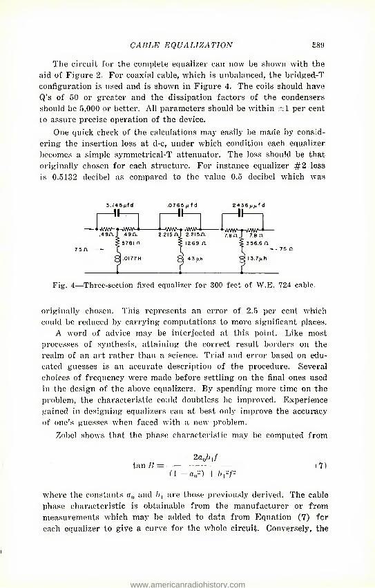
CABLE EQUALIZATION 589
The circuit for the complete equalizer can now be shown with the aid of Figure 2. For coaxial cable, which is unbalanced, the bridged-T configuration is used and is shown in Figure 4. The coils should have Q's of 50 or greater and the dissipation factors of the condensers should be 5,000 or better. All parameters should be within ±1 per cent to assure precise operation of the device.
One quick check of the calculations may easily be made by consid- ering the insertion loss at d-c, under which condition each equalizer becomes a simple symmetrical-T attenuator. The loss should be that originally chosen for each structure. For instance equalizer #2 loss is 0.5132 decibel as compared to the value 0.5 decibel which was
3.l45«fd .07 65 n f d 2436^ufd
Fig. 4—Three-section fixed equalizer for 300 feet of W.E. 724 cable.
originally chosen. This represents an error of 2.5 per cent whdch could be reduced by carrying computations to more significant places.
A word of advice may be interjected at this point. Like most processes of synthesis, attaining the correct result borders on the realm of an art rather than a science. Trial and error based on edu- cated guesses is an accurate description of the procedure. Several choices of frequency were made before settling on the final ones used in the design of the above equalizers. By spending more time on the problem, the characteristic could doubtless be improved. Experience gained in designing equalizers can at best only improve the accuracy of one's guesses when faced with a new problem.
Zobel shows that the phase characteristic may be computed from
—2a0bJ tanB— (7)
n - a,,2) i /j|-/2
where the constants «u and hl are those previously derived. The cable phase characteristic is obtainable from the manufacturer or from measurements which may be added to data from Equation (7) for each equalizer to give a curve for the whole circuit. Conversely, the
www.americanradiohistory.com
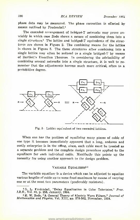
590 RCA REVIEW December 195 J,
phase data may be measured. The phase correction is effected by means outlined by Fredendall.4
The cascaded arrangement of bridged-T networks may prove un- wieldy in which case Bode shows a means of combining them into a single structure." The lattice and bridged-T equivalents of the struc- tures are shown in Figure 2. The combining means for the lattice is shown in Figure 5. The three structures after combining into a single lattice may often be reduced to a single bridged-T by means of Bartlett's Bisection Theorem. In considering the advisability of combining several networks into a single structure, it is well to re- member that the adjustments become much more critical, often to a prohibitive degree.
Fig. 5—Lattice equivalent of two cascaded lattices.
When one has the problem of equalizing many pieces of cable of one type it becomes immediately apparent that a long, arduous and costly enterprise is in the offing, since, each cable must be treated as a separate problem and the complete design procedure applied to the equalizers for each individual cable. Manifestly this points up the necessity for using another approach to the design problem.
Variable Equalizers23
The variable equalizer is a device which can be adjusted to equalize various lengths of cable up to some fixed maximum by means of varying one or at the most two parameters (preferably resistors).
4 G. L. Fredendall, "Delay Equalization in Color Television," Proc. I.R.E., Vol. 42, p. 258, January, 1954.
5 H. W. Bode, "A General Theory of Electric Wave Filters," Journal of Mathematics and Physics, Vol. XIII, pp. 275-362, November, 1934.
www.americanradiohistory.com
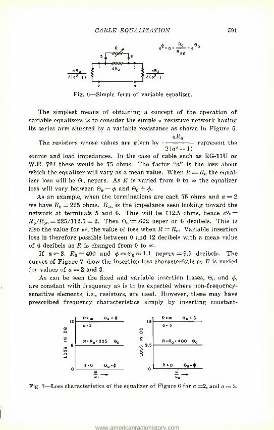
CABLE EQUALIZATION 591
0 Rn 2(- I )
-i—WWW—•- aR„
t1 C * = f
aRo ■2(o2-I
Fig. 6—Simple form of variable equalizer.
The simplest means of obtaining a concept of the operation of variable equalizers is to consider the simple tt resistive network having its series arm shunted by a variable resistance as shown in Figure 6.
aRo The resistors whose values are given bv represent the
2 (a- — 1) source and load impedances. In the case of cable such as KG-11U or W.E. 724 these would be 75 ohms. The factor "a" is the loss about which the equalizer will vary as a mean value. When R = Ru the equal- izer loss will be 0O nepers. As R is varied from 0 to <» the equalizer loss will vary between 0O — <£ and 0O + </>.
As an example, when the terminations are each 75 ohms and a = 2 we have R0 = 225 ohms. R:.t-, is the impedance seen looking toward the network at terminals 5 and 6. This will be 112.5 ohms, hence e% = i?0/i?56 = 225/112.5 = 2. Then 0O = .692 neper or 6 decibels. This is also the value for e^, the value of loss when R = R0. Variable insertion loss is therefore possible between 0 and 12 decibels with a mean value of 6 decibels as R is changed from 0 to co.
If a = 3, Rq = 400 and 4> nepers = 9.5 decibels. The curves of Figure 7 show the insertion loss characteristic as R is varied for values of a = 2 and 3.
As can be seen the fixed and variable insertion losses, 0n and <^, are constant with frequency as is to be expected where non-frequency- sensitive elements, i.e., resistors, are used. However, these may have prescribed frequency characteristics simply by inserting constant-
R = oo -Go ^
R=R„=225
R = O - d
9.5
R = oo ■Go + 0 0 = 3
R ~ RQ s 4 00 -OQ
R = O
Fig. 7—Loss characteristics of the equalizer of Figure 6 for a =2, and a = 3.
www.americanradiohistory.com
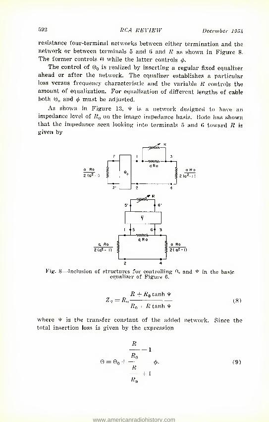
592 RCA REVIEW December 195^
resistance four-terminal networks between either termination and the network or between terminals 5 and 6 and R as shown in Figure 8. The former controls 0 while the latter controls <t>.
The control of ©0 is realized by inserting a regular fixed equalizer ahead or after the network. The equalizer establishes a particular loss versus frequency characteristic and the variable R controls the amount of equalization. For equalization of different lengths of cable both ©q and <£ must be adjusted.
As shown in Figure 13, + is a network designed to have an impedance level of R0 on the image impedance basis. Bode has shown that the impedance seen looking into terminals 5 and (i toward R is given by
Fig. 8—Inclusion of structures for controlling 0„ and 'I' in the basic equalizer of Figure 6.
R + Rn tanh + Z.. = R{) (8)
Rn R tanh ^
where + is the transfer constant of the added network. Since the total insertion loss is given by the expression
R 1 R.
0 = 0o + </>• (9) R
- + 1 Rn
www.americanradiohistory.com
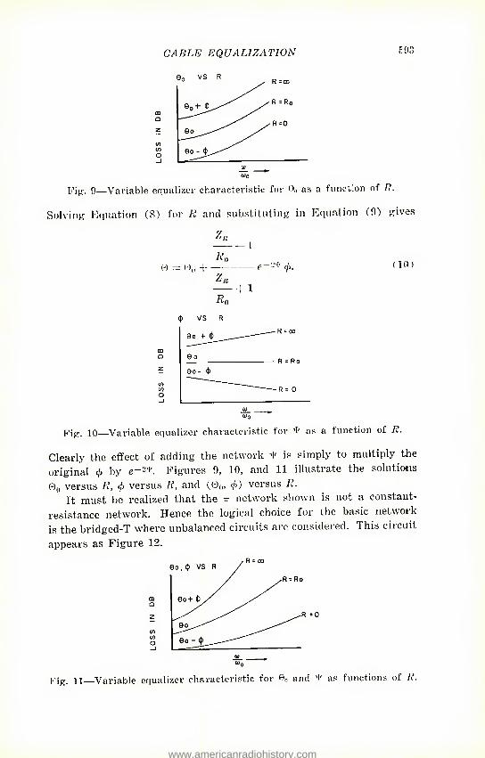
CABLE EQUALIZATION
U)q Pig. 9—Variable equalizer characteristic for 00 as a funct'.on of li.
Solving Equation (8) for /v and substituting in Equation (9) gives
Zu
OJ OJq
Fig'. 10—Variable equalizer characteristic for 'I' as a function of R.
Clearly the effect of adding the network * is simply to multiply the original </> by e-2* Figures 9, 10, and 11 illustrate the solutions 0O versus R, 4> versus R, and (0O, </>) versus R.
It must be realized that the tt network shown is not a constant- resistance network. Hence the logical choice for the basic network is the bridged-T where unbalanced circuits are considered. This circuit appears as Figure 12.
<"0 Fig. ii Variable equalizer characteristic for Oo and vl' as functions of R.
www.americanradiohistory.com
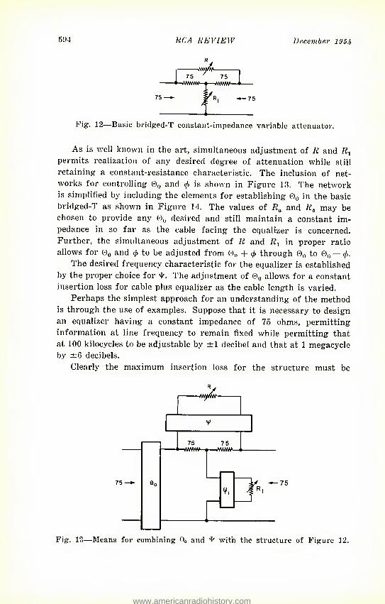
594 RCA REVIEW December 1954
75 VAWAV-
75 -MVAV-
75 —► R
Fig. 12—Basic bridged-T constant-impedance variable attenuator.
As is well known in the art, simultaneous adjustment of R and K, permits realization of any desired degree of attenuation while still retaining a constant-resistance characteristic. The inclusion of net- works for controlling 0O and $ is shown in Figure 13. The network is simplified by including the elements for establishing 0O in the basic bridged-T as shown in Figure 14. The values of Ra and Rb may be chosen to provide any 0O desired and still maintain a constant im- pedance in so far as the cable facing the equalizer is concerned. Further, the simultaneous adjustment of R and Rx in proper ratio allows for 0O and to be adjusted from 0O + <£ through 0O to 0O — <£.
The desired frequency characteristic for the equalizer is established by the proper choice for M'. The adjustment of 0,, allows for a constant insertion loss for cable plus equalizer as the cable length is varied.
Perhaps the simplest approach for an understanding of the method is through the use of examples. Suppose that it is necessary to design an equalizer having a constant impedance of 75 ohms, permitting information at line frequency to remain fixed while permitting that at 100 kilocycles to be adjustable by ±1 decibel and that at 1 megacycle by ±6 decibels.
Clearly the maximum insertion loss for the structure must be
75 VvVMV-
75 VyVMV-
75 —»
Fig. 13—Means for combining 9o and ^ with the structure of Figure 12.
www.americanradiohistory.com
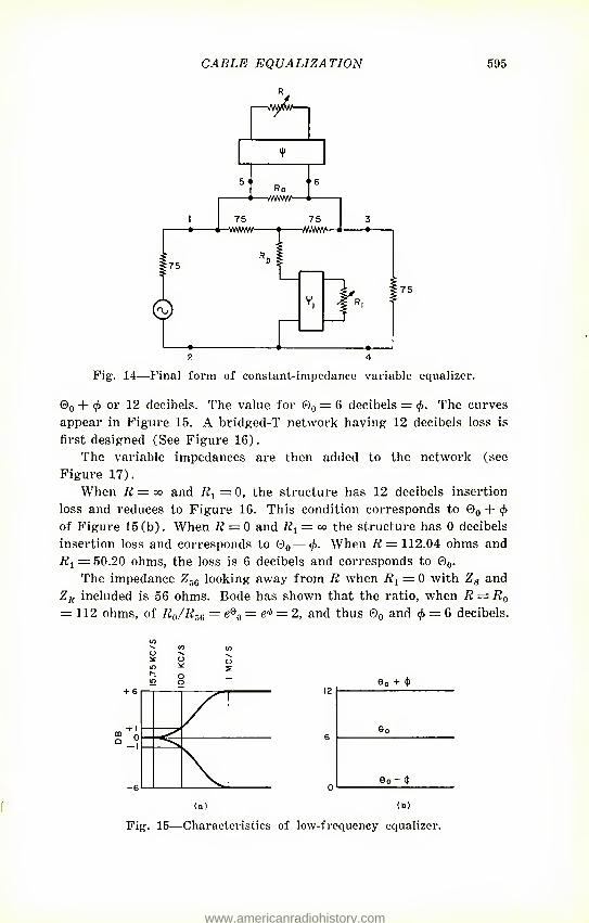
CABLE EQUALIZATION 595
Fig. 14—Final form of constant-impedance variable equalizer.
&Q + (j> or 12 decibels. The value for 0O = 6 decibels = 4>. The curves appear in Figure 15. A bridged-T network having 12 decibels loss is first designed (See Figure 16).
The variable impedances are then added to the network (see Figure 17).
When R = <x and R1 = 0, the structure has 12 decibels insertion loss and reduces to Figure 16. This condition corresponds to ©„ + </) of Figure 15 (b). When R — 0 and Rl = oo the structure has 0 decibels insertion loss and corresponds to 0O — </>. When R = 112.04 ohms and R1 = 50.20 ohms, the loss is 6 decibels and corresponds to 0O.
The impedance Zri6 looking away from R when iij = 0 with Zs and ZK included is 56 ohms. Bode has shown that the ratio, when R — R(t
— 112 ohms, of R0/Rr)6 = e0o = e^1 = 2, and thus 0O and (j> = G decibels.
V) ^ to CO o -v ^ ^ ^ o in ^ ^ o ^ o 00 + ^
(a) (b)
Fig. 15—Characteristics of low-frequency equalizer.
www.americanradiohistory.com
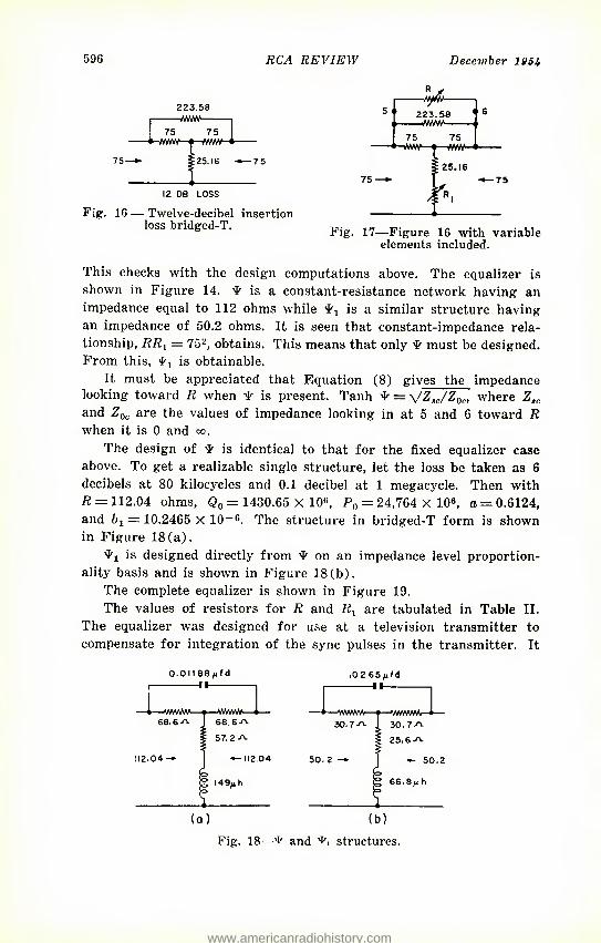
596 RCA REVIEW Deceviber 1951^
223.58 —VMW
75 75 -VvVVW » vWvW-
—— 223.58
—AWW-— 75
-vVW- ►25.16
75 ■ 12 DB LOSS
Fig. 16 — Twelve-decibel insertion loss bridged-T.
75 —vVWA- 25.16
Pig. 17—Figure 16 with variable elements included.
This checks with the design computations above. The equalizer is shown in Figure 14. ^ is a constant-resistance network having an impedance equal to 112 ohms while *fr1 is a similar structure having an impedance of 50.2 ohms. It is seen that constant-impedance rela- tionship, RR^ = 75-, obtains. This means that only ^ must be designed. From this, is obtainable.
It must be appreciated that Equation (8) gives the impedance looking toward R when ^ is present. Tanh * = yJZ^/Z^., where Z,r
and Z(}c are the values of impedance looking in at 5 and 6 toward R when it is 0 and ».
The design of ^ is identical to that for the fixed equalizer case above. To get a realizable single structure, let the loss be taken as 6 decibels at 80 kilocycles and 0.1 decibel at 1 megacycle. Then with /? = 112.04 ohms, Q0 = 1430.65 X 10«, P() = 24,764 X 108, a= 0.6124, and = 10.2465 X 10_R. The structure in bridged-T form is shown in Figure 18(a).
is designed directly from ^ on an impedance level proportion- ality basis and is shown in Figure 18 (b).
The complete equalizer is shown in Figure 19. The values of resistors for R and ^ are tabulated in Table II.
The equalizer was designed for use at a television transmitter to compensate for integration of the sync pulses in the transmitter. It
O. O I I 88 /i f d 1 ■
— —WMW- 68.6^ 57. 2-A.
149/1 h
(q) (b)
Fig. 18—+ and 't'l structures.
www.americanradiohistory.com
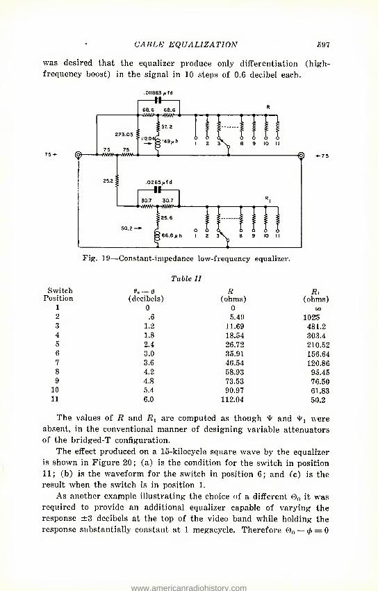
CABLE EQUALIZATION 597
was desired that the equalizer produce only differentiation (high- frequency boost) in the signal in 10 steps of 0.6 decibel each.
.011883 n<i If—|
G8.6 68. G R
1149/1 h 75 75 —yVMV-*—AVvW—<
.0265/if d -HI 30.7 30.7
-yWW-f-vVAW-
> 66.8 /i h
Fig. 19—Constant-impedance low-frequency equalizer.
Table II Switch — p R R*
Position (decibels) (ohms) (ohms) 1 0 0 ao 2 .6 5.49 1025 3 1.2 11.69 481.2 4 1.8 18.54 303.4 5 2.4 26.72 210.E2 6 3.0 35.91 156.64 7 3.6 46.54 120.86 8 4.2 58.93 95.45 9 4.8 73.53 76.50
10 5.4 90.97 61.83 11 6.0 112.04 50.2
The values of R and R] are computed as though ^ and ^ were absent, in the conventional manner of designing variable attenuators of the bridged-T configuration.
The effect produced on a 15-kilocycle square wave by the equalizer is shown in Figure 20; (a) is the condition for the switch in position 11; (b) is the waveform for the switch in position 6; and (c) is the result when the switch is in position 1.
As another example illustratinK the choice of a different 0n it was required to provide an additional equalizer capable of varying the response ±3 decibels at the top of the video band while holding the response substantially constant at 1 megacycle. Therefore 0O — 0 = 0
www.americanradiohistory.com
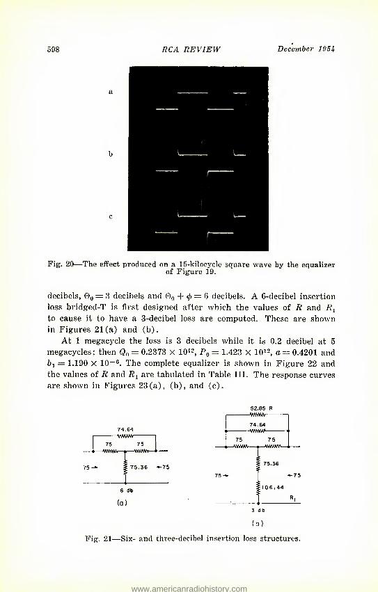
598 RCA REVIEW December 1954
b
a
c
Fig. 20—The effect produced on a 15-kilocycle square wave by the equalizer of Figure 19.
decibels, ©o:=: ^ decibels and 0O + = 6 decibels. A 6-decibel insertion loss bridged-T is first designed after which the values of R and Rl
to cause it to have a 3-decibel loss are computed. These are shown in Figures 21(a) and (b).
At 1 megacycle the loss is 3 decibels while it is 0.2 decibel at 5 megacycles; then Q0 = 0.2373 X 10¹², P0 = 1.423 X 10¹², a = 0.4201 and bx = 1.190 X lO-0. The complete equalizer is shown in Figure 22 and the values of R and R] are tabulated in Table III. The response curves are shown in Figures 23(a), (b), and (c).
52.85 R -WAWv 74 .64 74.64
-WAWr 75 75 75 -VAWvV
75 AVvYAV i—WAWv —WyW/A-
75.36 ♦-75 75,36 75 75 75
6 db
3 db
(b)
Fig. 21—Six- and three-decibel insertion loss structures.
www.americanradiohistory.com
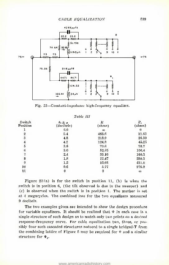
CABLE EQUALIZATION 599
AZGGiififd
Fig. 22—Constant-impedance high-frequency equalizer.
Table III Switch 6o± (ft R Ri
(ohms) Position (decibels) (ohms) 1 6.0 CO 0 2 5.4 483.6 11.63 3 4.8 213.9 26.30 4 4.2 124.3 45.25 5 3.6 79.6 70.7 6 3.0 52.85 106.4 7 2.4 35.10 160.3 8 1.8 22.47 250.3 9 1.2 13.05 431.0
10 0.6 5.77 975.0 11 0 0 CO
Figure 2,3 (a) is for the switch in position 11, (b) is when the switch is in position 6, (the tilt observed is due to the sweeper) and (c) is observed when the switch is in position 1. The marker is set at 4 megacycles. The combined loss for the two equalizers measured 9 decibels.
The two examples given are intended to show the design procedure for variable equalizers. It should be realized that ^ in each case is a single structure of such design as to match only two points on a desired response-frequency curve. For cable equalization two, three, or pos- sibly four such cascaded structures reduced to a single bridged-T from the combining lattice of Figure 5 may be required for ^ and a similar structure for •$■!.
www.americanradiohistory.com
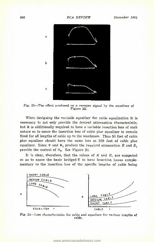
600 RCA REVIEW December 19 5 U
Fig. 23—The effect produced on a sweeper signal by the equalizer of Figure 22.
When designing the variable equalizer for cable equalization it is necessary to not only provide the desired attenuation characteristic, but it is additionally required to have a variable insertion loss of such nature as to cause the insertion loss of cable plus equalizer to remain fixed for all lengths of cable up to the maximum. Thus 50 feet of cable plus equalizer should have the same loss as 300 feet of cable plus equalizer. Since ^ and produce the required attenuation R and provide the control of 0O. See Figure 24.
It is clear, therefore, that the values of R and K, are computed so as to cause the basic bridged-T to have insertion losses comple- mentary to the Insertion loss of the specific lengths of cable being
Fig. 24—Loss characteristics for cable and equalizer for various lengths of cable.
www.americanradiohistory.com
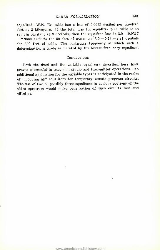
CABLE EQUALIZATION 601
equalized. W.E. 724 cable has a loss of 0.0633 decibel per hundred feet at 2 kilocycles. If the total loss for equalizer plus cable is to remain constant at 3 decibels, then the equalizer loss is 3.0 — 0.0317 = 2.9683 decibels for 50 feet of cable and 3.0 — 0.19 = 2.81 decibels for 300 feet of cable. The particular frequency at which such a determination is made is dictated by the lowest frequency equalized.
Conclusions
Both the fixed and the variable equalizers described here have proved successful in television studio and transmitter operations. An additional application for the variable types is anticipated in the realm of "mopping up" equalizers for temporary remote program circuits. The use of two or possibly three equalizers in various portions of the video spectrum would make equalization of such circuits fast and effective.
www.americanradiohistory.com
OBSERVED DIURNAL VARIATIONS IN
FREQUENCIES AND SIGNAL QUALITIES BETWEEN NEW YORK AND CENTRAL EUROPE*
By
J. H. Nelson
Engineering Department, KCA Communications, Inc., New York, N. Y.
Summary—This paper discusses variations in frequency requirements and signal qualities, as observed at the receiving station at Riverhead, N. Y. for the period November 1 to November 30, 1953 on shortwave signals being received from Central European points.
INCE July 1949 receiving-station technicians at Riverhead, N. Y. have been gathering data on radio propagation conditions for the purpose of signal analysis.1 ^ This data is required by the
forecaster of radio conditions in the preparation of the daily forecasts, since a systematic study of such data has made it possible to observe trends which indicate the future behavior of the signals.
Five reports are sent to the forecaster each day. These daily reports are made at 4:00 AM, 6:00 AM, 10:00 AM, 6:00 PM, and 10:00 PM Eastern Standard Time and refer to the highest, and lowest, frequency being received from Central Europe (encompassing London, Paris, Brussels, Amsterdam and Berne) and the quality of the signals in this band.
The data contained in these five reports for November 1953 has been transferred to graphs which are shown as Figures 1-5. Similar reports have been made by Riverhead for over four years.
* Decimal Classification: R113.74. 1 A. M. Arzinger, H. E. Hallborg, and J. H. Nelson, "Sunspots and
Radio Weather," RCA Review, Vol. IX, pp. 229-244, June, 1948. 2 J. H. Nelson, "Shortwave Radio Propagation Correlation with Plan-
etary Positions," RCA Review, Vol. XII, pp. 26-34, March, 1951. 3 J. H. Nelson, "Planetary Position Effects on Shortwave Signal
Quality," Elec. Eng., Vol. 71, pp. 421-424, May, 1952. 4 J. H. Nelson, "Radio Weather Forecasting Techniques," Transactions
of the I.R.E., Vol. CS-2, Number 1, pp. 19-23B, January, 1954.
Introduction
602
www.americanradiohistory.com
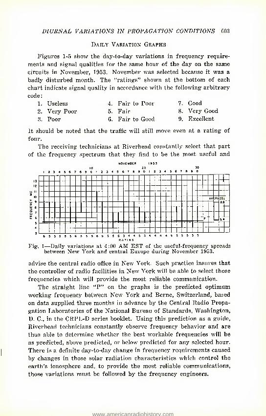
DIURNAL VARIATIONS IN PROPAGATION CONDITIONS 603
Daily Variation Graphs
Figures 1-5 show the day-to-day variations in frequency require- ments and signal qualities for the same hour of the day on the same circuits in November, 1953. November was selected because it was a badly disturbed month. The "ratings" shown at the bottom of each chart indicate signal quality in accordance with the following arbitrary code:
1. Useless 4. Fair to Poor 7. Good 2. Very Poor 5. Fair 8. Very Good 3. Poor 6. Fair to Good 9. Excellent
It should be noted that the traffic will still move even at a rating of four.
The receiving technicians at Riverhead constantly select that part of the frequency spectrum that they find to be the most useful and
i j 12
o 11 3 10 5 9 S 6 2 7
£ 6 5 4 3
Fig. 1—Daily variations at 4:00 AM EST of the useful-frequency spreads between New York and central Europe during November 1953.
advise the central radio office in New Yoi'k. Such practice insures that the controller of radio facilities in New York will be able to select those frequencies which will provide the most reliable communication.
The straight line "P" on the graphs is the predicted optimum working frequency between New York and Berne, Switzerland, based on data supplied three months in advance by the Central Radio Propa- gation Laboratories of the National Bureau of Standards, Washington, D. C., in the CRPL-D series booklet. Using this prediction as a guide. Riverhead technicians constantly observe frequency behavior and are thus able to determine whether the best workable frequencies will be as predicted, above predicted, or below predicted for any selected hour. There is a definite day-to-day change in frequency requirements caused by changes in those solar radiation characteristics which control the earth's ionosphere and, to provide the most reliable communications, those variations must be followed by the frequency engineers.
NOVEMBER 1953 10 20 30
I 2345678901 2345678901234567090
_ AV IRA GE
- p
T 1 1 1 1 655555655565555344534444555555
RATING
www.americanradiohistory.com
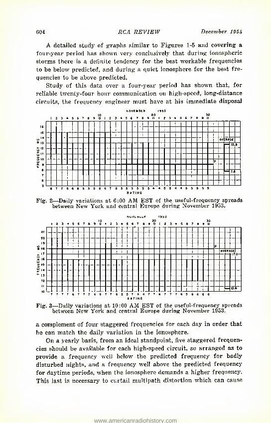
604 RCA REVIEW December 195^
A detailed study of graphs similar to Figures 1-5 and covering a four-year period has shown very conclusively that during ionospheric storms there is a definite tendency for the best workable frequencies to be below predicted, and during a quiet ionosphere for the best fre- quencies to be above predicted.
Study of this data over a four-year period has shown that, for reliable twenty-four hour communication on high-speed, long-distance circuits, the frequency engineer must have at his immediate disposal
NOVEMBER I 2 3 4 5 6 7 2 3 4 5 6 2 3 4 5 6 7
677666556667655555544554455555 RATING
Fig. 2—Daily variations at 6:00 AM EST of the useful-frequency spreads between New York and central Europe during' November 1953.
1234567890 No l/trducrt I 9S3
20 30 234567 8901234567890
AVERAGE 17.0- z 16 2 '5
77776777 66776557 66776777656666 RATING
Fig. 3—Daily variations at 10:00 AM EST of the useful-frequency spreads between New York and central Europe during November 1953.
a complement of four staggered frequencies for each day in order that he can match the daily variation in the ionosphere.
On a yearly basis, from an ideal standpoint, five staggered frequen- cies should be available for each high-speed circuit, so arranged as to pi'ovide a frequency well below the predicted frequency for badly disturbed nights, and a frequency well above the predicted frequency for daytime periods, when the ionosphere demands a higher frequency. This last is necessary to curtail multipath distortion which can cause
www.americanradiohistory.com
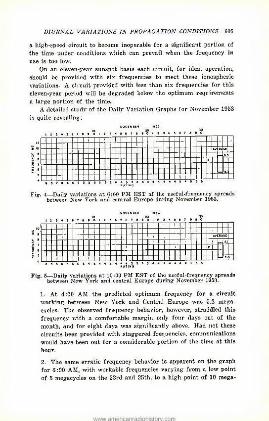
DIURNAL VARIATIONS IN PROPAGATION CONDITIONS 605
a high-speed circuit to become inoperable for a significant portion of the time under conditions which can prevail when the frequency in use is too low.
On an eleven-year sunspot basis each circuit, for ideal operation, should be provided with six frequencies to meet these ionospheric variations. A circuit provided with less than six frequencies for this eleven-year period will be degraded below the optimum requirements a large portion of the time.
A detailed study of the Daily Variation Graphs for November 1953 is quite revealing:
11 o S 10 v 9 o * 8 o T tr 6
5
Fig. 4—Daily variations at 6:00 PM EST of the useful-frequency spreads between New York and central Europe during November 1953.
10 u * > > « 0 1 7 s 6
Fig. 5—Daily variations at 10:00 PM EST of the useful-frequency spreads between New York and central Europe during November 1953.
1. At 4:00 AM the predicted optimum frequency for a circuit working between New York and Central Europe was 5.2 mega- cycles. The observed frequency behavior, however, straddled this frequency with a comfortable margin only four days out of the month, and for eight days was significantly above. Had not these circuits been provided with staggered frequencies, communications would have been out for a considerable portion of the time at this hour.
2. The same erratic frequency behavior is apparent on the graph for 6:00 AM, with workable frequencies varying from a low point of 5 megacycles on the 23rd and 25th, to a high point of 10 mega-
NOVEMBER 1953 10 20 30 1234567890123456789 01234567890
- AVERA r-1 0.3
p ■
_5.
NOVEMBER 1953 10 20 30 12345678901 23456789012 34567 890
| 1-14 5 656655555544344433354444444355 RATING
www.americanradiohistory.com
606 RCA REVIEW December 1954.
cycles on the 1st, 6th, and 12th. The best frequencies straddled the predicted optimum frequency comfortably about half of the month.
3. At 10:00 AM the workable frequency straddled the predicted frequency only seven days of the month. If the circuit did not have a complement of frequencies between 12 and 16 megacycles, severe difficulty would have been encountered throughout most of the month, even though the rating scale shows that at this period of the day only three days were recorded as moderately disturbed (5), the remainder of the month rated as (6) or (7) which is undisturbed.
4. The same pattern is apparent at 6:00 PM and 10:00 PM.
Conclusion
During the past ten years, substantial improvements have been made in the receivers, transmitters, and antennas used for long-range communications. Whereas speeds of 150 words per minute were con- sidered high ten years ago, today speeds of 240 words per minute are required on 4-channel multiplex circuits being used for teletype. It should be kept in mind, however, that this increase in capacity has been accompanied by an increase in traffic, so that further increases in capacity are necessary.
In order to provide the high-grade signals that are required for this high-speed communication, it is necessary that the frequency engineer be able to meet the fickle demands of the ionosphere as closely as possible. He can do this only if he has the proper frequency complement at his disposal. Often the difference between an unwork- able circuit and a workable circuit is only one megacycle.
www.americanradiohistory.com
RCA TECHNICAL PAPERS!
Third Quarter, 1954
Any request for copies of papers listed herein should be addressed to the publications to which credited.*
"An Analysis of the Bifilar-T Trap Circuit," B. Fisher and J. Avins, RCA Industry Service Laboratory Bulletin LB-961 (Septem- ber 16) 1954
"Circular Polarization in Waveguides and Cavities," R. W. Klopfen- stein, RCA Review (September) 1954
"Color Stripe Added to Station's Monochrome Signal," E. E. Gloy- stein. Broadcast News (July-August) 1954
"Commercial Aspects of UHF Booster Operation," L. W. Haeseler, N. McNaughten, and L. J. Wolf, Broadcast News (July- August) 1954
"Compact Three-Set Color Studio," M. G. Moon, Broadcast News (July-August) 1954
"Comparative High-Frequency Operation of Junction Transistors Made of Different Semiconductor Materials," L. J. Giacoletto, RCA Industry Service Laboratory Bulletin LB-963 (September 24) 1954
"Comparison of Various Approximate Exchange Potentials," F. Her- man, J. Callaway, and F. S.. Acton, Phys. Rev. (July 15) .... 1954
"The Complete Specification of a Network by a Single Parameter," M. S. Corrington, T. Murakami, and R. W. Sonnenfeldt, RCA Review (September) 1954
"Components for Pi-Coupled Amplifiers," M. Seybold, Ham Tips (July-August) 1954
"A Convergence Circuit for the RCA Developmental 21-Inch Color Kinescope," M. D. Nelson, RCA Industry Service Laboratory Bulletin LB-960 (September 16) 1954
"The CT-100 Commercial Color Television Receiver," L. R. Kirkwood and A. J. Torre, RCA Review (September) 1954
"Damping of Loudspeaker Cabinet Panels," M. Rettinger, Audio (September) 1954
"A Developmental Pocket-Size Broadcast Receiver Employing Tran- sistors," L. A. Freedman, T. O. Stanley, and D. D. Holmes, RCA Industry Service Laboratory Bulletin LB-957 (August 23) 1954
"The Effective Surface Recombination of a Germanium Surface with a Floating Barrier," A. R. Moore and W. M. Webster, RCA Industry Service Laboratory Bulletin LB-9S3 (July 2) 1954
"Electron Microscopy of Ultra-Thin Sections of Insect Flight Muscle," G. B. Chapman, Journal of Morphology (September) 1954
"Engineering Aspects of UHF Booster Installation," J. Epstein, W. C. Morrison, and O. M. Woodward, Jr., Broadcast News (July-August) 1954
t Report all corrections or additions to RCA Review, RCA Laboratories. Princeton. N. J. * RCA Industry Service Laboratory Bidletins are not published and are issued only as
a service to licensees of the Radio Corporation of America. 607
www.americanradiohistory.com
608 RCA REVIFAV December 195 A
"An Experimental Automobile Receiver Employing Transistors," D. D. Holmes, T. 0. Stanley, and L. A. Freedman, RCA Indus- try Service Laboratory Bulletin LB-958 (August 23) 1954
"An Exploration of the Effects of Strong Radio-Frequency Fields on Micro-Organisms in Aqueous Solutions," G. H. Brown and W. C. Morrison, Food Technology (August) 1954
"Facsimile Scanning by Cathode-Ray Tube," W. H. Bliss and C. J. Young, RCA Review (September) 1954
"Factors in the Design of Keyed Clamping Circuits," R. N. Rhodes, RCA Review (September) 1954
"Formation of Single Crystal Silicon Fibers," E. R. Johnson and J. A. Amick, Jour. Appl. Phys. (September) (Letter to the Editor) 1954
"High-Level Triode Color Demodulator," A. Macovski, RCA Industry Service Laboratory Bulletin LB-959 (September 16) 1954
"Importance of Thermal Equilibrium in Measurements on Powdered Insulators in Vacuo," R. H. Bube and R. E. Shrader, Rev. Sci. Instr. (September) (Letter to the Editor) 1954
"Increased Light Sensitivity from Standard Gas Phototubes," E. 0. Johnson, Rev. Sci. Instr. (August) 1954
"An Investigation of the Ultimate Performance of Space-Charge Deflection Tubes," J. T. Wallmark, Proc. I.R.E. (September) 1954
"Microwave Link for Worldwide Communication," C. H. Backus and S. Lapenson, Radio Electronic Engineering (September)..., 1954
"Monochrome Vidicon Film Camera," W. L. Hurford and R. J. Marian, RCA Revietv (September) 1954
"On the Heats of Sublimation and Evaporation of Germanium," R. E. Honig, Jour. Chem. Phys. (September) (Letter to the Editor) 1954
"Plating Applications in the Television Field," L. Fox, Plating (July) 1954 "Polarographic Determination of Zinc in Gold," S. B. Deal, Analytical
Chemistry (September) 1954 "Pulsed Curve Tracer for Semiconductor Testing," J. I. Pankove,
Electronics (September) 1954 "A Review of Twenty-Five Years of Sound Reproduction," H. F.
Olson, Jour. Acous. Soc. Amer. (September) 1954 "Saturation Current in Alloy Junctions," W. M. Webster, RCA
Industry Service Laboratory Bulletin LB-956 (August 12) . . . 1954 "A Silicon N-P-N Junction Transistor by the Alloy Process," H. Nel-
son, RCA Industry Service Laboratory Bulletin LB-952 (July 2) 1954
"A Simplified High-Performance 21-Inch Developmental Color Tele- vision Receiver," RCA Industry Service Laboratory Bulletin LB-962 (September 16) 1954
"Some Properties of Germanium-Silicon Alloys." E. R. Johnson and S. M. Christian, Phys. Rev. (July 15) (Letter to the Editor) 1954
"Speculations on the Energy Band Structure of Ge-Si Alloys," F. Her- man, Phys. Rev. (August 1) (Letter to the Editor) 1954
"Studies of the Interface Layer in Oxide Cathodes," L. S. Nergaard and R. M. Matheson, RCA Review (September) 1954
"Sublimation Studies of Silicon in the Mass Spectrometer," R. E. Honig, Jour. Chem. Phys. (September) (Letter to the Editor) 1954
"The Tacitron, A Low Noise Thyatron Capable of Current Inter- ruption by Grid Action." E. O. Johnson, J. Olmstead, and W. M. Webster, Proc. I.R.E (September) 1954
"Television Transmitter Considerations in Color Broadcasting," T. M. Gluyas, Jr.. RCA Review (September) 1954
"Transmitter Relay Control Systems," R. M. Crotinger, Broadcast News (July-August) 1954
www.americanradiohistory.com
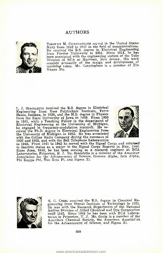
AUTHORS
Timothy M. Cunningham served in the United States Navy from 1942 to 1947 in the field of communications. He received the B.S. degree in Electrical Engineering from Purdue University in 1951. Since 1951, he has been associated with the engineering section of the Tube Division of RCA at Harrison, New Jersey. His work consists primarily of the design and development of receiving tubes. Mr. Cunningham is a member of Eta Kappa Nu.
L. J. Giacoletto received the B.S. degree in Electrical Engineering from Rose Polytechnic Institute, Terre Haute, Indiana, in 1938, and the M.S. degree in Physics from the State University of Iowa in 1939. From 1939 to 1941, while a Teaching Fellow in the department of Electrical Engineering at the University of Michigan, he engaged in frequency-modulation research. He re- ceived the Ph.D. degree in Electrical Engineering from the University of Michigan in 1952. He was associated j with the Collins Radio Company during the summers of ' 1937 and 1938, and with the Bell Telephone Laboratories in 1940. From 1941 to 1945 he served with the Signal Corps and returned to inactive status as a major in the Signal Corps Reserve in May, 1946. Since June, 1946, he has been serving as a research engineer at RCA Laboratories, Princeton, N. J. Dr. Giacoletto is a member of the American Association for the Advancement of Science, Gamma Alpha, Iota Alpha, Phi Kappa Phi, Tau Beta Pi, and Sigma Xi.
H. G. Greig received the B.S. degree in Chemical En- gineering from Drexel Institute of Technology in 1931. He was with the Research Department of the National Aniline Division of Allied Chemical and Dye Corporation until 1943. Since 1943 he has been with RCA Labora- tories in Princeton, N. J. Mr. Greig is a member of the American Chemical Society, the American Association for the Advancement of Science, and Sigma Xi.
www.americanradiohistory.com
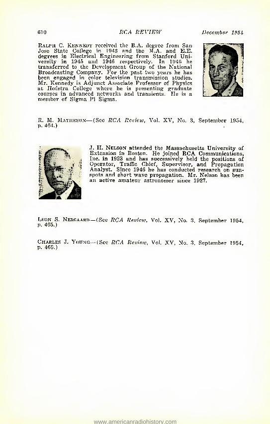
610 RCA REVIEW December 195 Jt
Ralph C. Kennedy received the B.A. degree from San Jose State College in 1943 and the M.A. and E.E. degrees in Electrical Engineering from Stanford Uni- versity in 1945 and 1946 respectively. In 1946 he transferred to the Development Group of the National Broadcasting Company. For the past two years he has been engaged in color television transmission studies. Mr. Kennedy is Adjunct Associate Professor of Physics at Hofstra College where he is presenting graduate courses in advanced networks and transients. He is a member of Sigma Pi Sigma.
R. M. Matheson—(See RCA Review, Vol. XV, No. 3, September 1954, p. 464.)
J. H. Nelson attended the Massachusetts University of Extension in Boston. He joined RCA Communications, Inc. in 1923 and has successively held the positions of Operator, Traffic Chief, Supervisor, and Propagation Analyst. Since 1946 he has conducted research on sun- spots and short wave propagation. Mr. Nelson has been an active amateur astronomer since 1927.
Leon S. Nergaard—(See RCA Review, Vol. XV, No. p. 465.)
Charles J. Young—(See RCA Review, Vol. XV, No. p. 465.)
3, September 1954,
3, September 1954,
www.americanradiohistory.com
RCA REVIEW
a technical journal
RADIO AND ELECTRONICS RESEARCH • ENGINEERING
INDEX
VOLUME XV
Table op Contents
March PAGE
A System for Recording and Reproducing Television Signals 3 H. F. Olson, W. D. Houghton, A. R. Morgan, J. Zenel
M. Artzt, J. G. Woodward, and J. T. Fischer A Symmetrical Transistor Phase Detector for Horizontal Synchroni-
zation B. Harris and A. Macovski
Investigation of Ultra-High-Frequency Television Amplifier Tubes . . 27 W. Y. Pan
Ceramic-Metal Seals of the Tungsten-Iron Type ^6 D. G. Burnside
Filter Using Coaxial Transmission Line as Elements 62 H. B. Yin and T. U. Foley
Recrystallization of Germanium from Indium Solution 75 J. I. Pankove
A Demountable Vacuum System for Electron-Tube Development .... 86 T. M. Shrader
Transmission-Line Analog of a Modulated Electron Beam 95 S. Bloom and R. W. Peter
Space-Charge-Wave Amplification Along an Electron Beam by Periodic Change of the Beam Impedance 113
R. W. Peter, S. Bloom, and J. A. Ruetz High-Frequency Operation of P-Type Point-Contact Transistors .... 121
F. L. Hunter and B. N. Slade
June
The Metrechon—A Halftone-Picture Storage Tube 145 L. Pbnsak
Synthesis of Constant-Time-Delay Networks 163 M. S. Corrington and R. W. Sonnenfeldt
Synthetic-Pattern Generator for the Solution of Certain Instru- mentation Problems in Television 187
R. C. Webb Broadbanding of Resonant-Tvpe Microwave Output Windows 204
T. S. Chen 611
www.americanradiohistory.com
G12 RCA REVIEW December 195Jt
PAGE Design Considerations for Frequency-Shift-Keyed Circuits 230
W. Lyons Application of Brewster's Angle to the Design of Coaxial-Line Com-
ponents for Microwaves 238 B. A. Dahlman
A Minimum Noise Figure for the Traveling-Wave Tube 252 S. Bloom and R. W. Peter
September
Facsimile Scanning by Cathode-Ray Tube 275 W. H. Bliss and C. J. Young
Circular Polarization in Waveguides and Cavities 291 R. W. KlopfenSTEIN
Television Transmitter Considerations in Color Broadcasting 312 T. M. Gluyas, Jr.
Studies of the Interface Layer in Oxide Cathodes 335 L. E, Nergaard and R. M. Matheson
Factors in the Design of Keyed Clamping Circuits 362 R. N. Rhodes
Monochrome Vidicon Film Camera 372 W. L. Hurford and R. J. Marian
The Complete Specification of a Network by a Single Parameter .... 389 M. S. Corrington, T. Murakami, and R. W. Sonnenfeldt
The CT-100 Commercial Color Television Receiver 445 L. R. Kirkwood and A. J. Torre
December
"Electrofax"—Direct Electrophotographic Printing on Paper 469 C. J. Young and H. G. Greig
A Bridge for the Measurement of Cathode Impedance 485 R. M. Matheson and L. S. Nergarrd
Study of P-N-P Alloy Junction Transistor from D-C through Medium Frequencies 506
L. J. Giacolbtto Practical Considerations in the Design of Low-Microphonic Tubes . . 563
T. M. Cunningham Cable Equalization for Television Studio Circuits 581
R. C. Kennedy Observed Diurnal Variations in Frequencies and Signal Qualities
between New York and Central Europe 602 J. H. Nelson
Index, Volume XV issue page
"Application of Brewster's Angle to the Design of Coaxial-Line Components for Microwaves," B. A. Dahlman June 238
"A Bridge for the Measurement of Cathode Impedance," R. M. Matheson and L. S. Nergaard Dec. 485
"Broadbanding of Resonant-Type Microwave Output Windows," T. S. Chen June 204
"Cable Equalization for Television Studio Circuits," R. C. Kennedy Dec. 581
www.americanradiohistory.com
INDEX 613
ISSUE PAGE "Ceramic-Metal Seals of the Tungsten-Iron Type," D. G. Burn-
side Mar. 46 "Circular Polarization in Waveguides and Cavities," R. W.
Klopfenstein Sept. 291 "The Complete Specification of a Network by a Single Param-
eter," M. S. Corrington, T, Murakami, and R. W. Sonnen- feldt Sept. 389
"The CT-100 Commercial Color Television Receiver," L. R. Kirkwood and A. J. Torre Sept. 445
"A Demountable Vacuum System for Electron-Tube Develop- ment," T. M. Shrader Mar. 86
"Design Considerations for Frequency-Shift-Keyed Circuits," W. Lyons June 230
" 'Electrofax'—Direct Electrophotographic Printing on Paper," C. J. Young and H. G. Greig Dec. 469
"Facsimile Scanning by Cathode-Ray Tube," W. H. Bliss and C. J. Young Sept. 275
"Factors in the Design of Keyed Clamping Circuits," R. N. Rhodes Sept. 362
"Filter Using Coaxial Transmission Line as Elements," H. B. Yin and T. U. Foley Mar. 62
"High-Frequency Operation of P-Type Point-Contract Tran- sistors," F. L. Hunter and B. N. Slade Mar. 121
"Investigation of Ultra-High-Frequency Television Amplifier Tubes," W. Y. Pan Mar. 27
"The Metrechon—A Halftone-Picture Storage Tube," L. Pensak June 145 "A Minimum Noise Figure for the Traveling-Wave Tube,"
S. Bloom and R. W. Peter June 252 "Monochrome Vidicon Film Camera," W. L. Hurford and R. J.
Marian Sept. 372 "Observed Diurnal Variations in Frequencies and Signal Quali-
ties between New York and Central Europe," J. H. Nelson Dec. 602 "Practical Considerations in the Design of Low-Microphonic
Tubes," T. M. Cunningham Dec. 563 "Recrystallization of Germanium from Indium Solution," J. I.
Pankove Mar. 75 "Space-Charge-Wave Amplification Along an Electron Beam by
Periodic Change of the Beam Impedance," R. W. Peter, S. Bloom and J. A. Ruetz Mar. 113
"Studies of the Interface Layer in Oxide Cathodes," L. S. Nergaard and R. M. Matheson Sept. 335
"Study of P-N-P Alloy Junction Transistor from D-C through Medium Frequencies," L. J. Giacoletto Dec. 506
"A Symmetrical Transistor Phase Detector for Horizontal Syn- chronization," B. Harris and A. Macovski Mar. 18
"Synthesis of Constant-Time-Delay Networks," M. S. Corrington and R. W. Sonnenfeldt June 163
"Synthetic-Pattern Generator for the Solution of Certain Instru- mentation Problems in Television," R. C. Webb June 187
"A System for Recording and Reproducing Television Signals," H. F. Olson, W. D. Houghton, A. R. Morgan, J. Zenel, M.
Artzt, J. G. Woodward, and J. T. Fischer Mar. 3 "Television Transmitter Considerations in Color Broadcasting,"
T. M. Gluyas, Jr Sept. 312 "Transmission-Line Analog of a Modulated Electron Beam,"
S. Bloom and R. W. Peter Mar. 95
www.americanradiohistory.com
614 RCA REVIEW December 195i
Authors, Volume XV ISSUE PAGE
Artzt, M. (Coauthor)—"A System for Recording and Repro- ducing Television Signals" Mar. 3
Bliss, W. H. (Coauthor)—"Facsimile Scanning by Cathode-Ray Tube" Sept. 275
Bloom, S. (Coauthor)—"A Minimum Noise Figure for the Traveling-Wave Tube" June 252 "Space-Charge-Wave Amplification Along an Electron Beam by Periodic Change of the Beam Impedance" Mar. 113 "Transmission-Line Analog of a Modulated Electron Beam" Mar. 95
Burnside, D. G.—"Ceramic-Metal Seals of the Tungsten-Iron Type" Mar. 46
Chen, T. S.—"Broadbanding of Resonant-Type Microwave Out- put Windows" June 204
Corrington, M. S. (Coauthor)—"The Complete Specification of a Network by a Single Parameter" Sept. 389 "Synthesis of Constant-Time-Delay Networks" June 163
Cunningham, T. M.—■"Practical Considerations in the Design of Low-Microphonic Tubes" Dec. 563
Dahlman, B. A.—"Application of Brewster's Angle- to the De- sign of Coaxial-Line Components for Microwaves" June 238
Fischer, J. T. (Coauthor)—"A System for Recording and Re- producing Television Signals" Mar. 3
Foley, T. U. (Coauthor)—"Filter Using Coaxial Transmission Line as Elements" Mar. 62
Giacoletto, L. J.—"Study of P-N-P Alloy Junction Transistor from D-C through Medium Frequencies Dec 506
Gluyas, T. M., Jr.—"Television Transmitter Considerations in Color Broadcasting" Sept. 312
Greig, H. G. (Coauthor)—"'Electrofax'—Direct Electrophoto- graphic Printing on Paper" Dec. 469
Harris, B. (Coauthor)—"A Symmetrical Transistor Phase De- tector for Horizontal Synchronization" Mar. 18
Houghton, W. D. (Coauthor)—-"A System for Recording and Re- producing Television Signals" Mar. 3
Hunter, F. L. (Coauthor)—"High-Frequency Operation of P- Type Point-Contact Transistors" Mar. 121
Hurford, W. L. (Coauthor)—"Monochrome Vidicon Film Camera" Sept. 372
Kennedy, R. C.—"Cable Equalization for Television Studio Cir- cuits" Dec. 581
Kirkwood, L. R. (Coauthor)—"The CT-100 Commercial Color Television Receiver" Sept. 445
Klopfenstein, R. W.—"Circular Polarization in Waveguides and Cavities" Sept. 291
Lyons, W.—"Design Considerations for Frequency-Shift-Keyed Circuits" June 230
Macovski, A. (Coauthor)—"A Symmetrical Transistor Phase Detector for Horizontal Synchronization" Mar. 18
Marian, R. J. (Coauthor)—"Monochrome Vidicon Film Camera" Sept. 372 Matheson, R. M. (Coauthor)—"A Bridge for the Measurement
of Cathode Impedance" Dec. 485 "Studies of the Interface Layer in Oxide Cathodes" Sept. 335
Morgan, A. R. (Coauthor)—"A System for Recording and Re- producing Television Signals" Mar. 3
www.americanradiohistory.com
INDEX 615
ISSUE PAGE Murakami, T. (Coauthor)—"The Complete Specification of a
Network by a Sing-le Parameter" Sept. 389 Nelson, J. H.—"Observed Diurnal Variations in Frequencies
and Signal Qualities between New York and Central Europe" Dec. 602
Nergaard, L. S. (Coauthor)—"A Bridge for the Measurement of Cathode Impedance" Dec. 485 "Studies of the Interface Layer in Oxide Cathodes" Sept. 335
Olson, H. P. (Coauthor)—"A System for Recording- and Repro- ducing Television Signals" Mar. 3
Pan, W. J.—"Investigation of Ultra-High-Frequency Television Amplifier Tubes" Mar. 27
Pankove, J. I.—"Recrystallization of Germanium from Indium Solution" Mar. 76
Pensak, L.—-"The Metrechon—A Halftone-Picture Storage Tube" June 145 Peter, R. W. (Coauthor)—"A Minimum Noise Figure for the
Traveling-Wave Tube" June 252 "Space-Charge-Wave Amplification Along an Electron Beam by Periodic Change of the Beam Impedance" Mar. 113 "Transmission-Line Analog of a Modulated Electron Beam" Mar. 95
Rhodes, R. N.—"Factors in the Design of Keyed Clamping Cir- cuits" Sept. 362
Ruetz, J. A. (Coauthor)—"Space-Charge-Wave Amplification Along an Electron Beam by Periodic Change of the Beam Impedance" Mar. 113
Shrades, T. M.—"A Demountable Vacuum for Electron-Tube Development" Mar. 86
Slade, B. N. (Coauthor)—"Hight-Frequency Operation of P- Type Point-Contact Transistors" Mar. 121
Sonnenfeldt, R. W. (Coauthor)—"The Complete Specification of a Network by a Single Parameter" Sept. 389 "Synthesis of Constant-Time-Delay Networks" June 163
Torre, A. J. (Coauthor)—"The CT-100 Commercial Color Tele- vision Receiver" Sept. 445
Webb, R. C.—"Synthetic-Pattern Generator for the Solution of Certain Instrumentation Problems in Television" June 187
Woodward, J. G. (Coauthor)—"A System for Recording and Re- producing- Television Signals" Mar. 3
Yin, H. B. (Coauthor)—"Filter Using Coaxial Transmission Line as Elements" Mar. 62
Young, C. J. (Coauthor)—"'Electrofax'—Direct Electrophoto- graphic Printing on Paper" Dec. 469 "Facsimile Scanning by Cathode-Ray Tube" Sept. 275
Zenel, J. (Coauthor)—"A System for Recording and Repro- ducing Television Signals" Mar. 3
www.americanradiohistory.com


![Literature Review 2017 - Monash Health · impact of RCA training in increasing students’ ability to conduct an RCA [8], as well as revealed challenges students faced in the last](https://img.pdfslide.us/doc/110x75/5e4afa8de8929a3e1046a4fb/literature-review-2017-monash-health-impact-of-rca-training-in-increasing-studentsa.jpg)