Embed Size (px)
Citation preview
Conducting Layered MaterialsDOI: 10.1002/ange.201104050
Rb4Sn5P4Se20: A Semimetallic Selenophosphate**In Chung, Kanishka Biswas, Jung-Hwan Song, John Androulakis, Konstantinos Chondroudis,Konstantinos M. Paraskevopoulos, Arthur J. Freeman, and Mercouri G. Kanatzidis*
Chalcophosphates are ternary (A/P/Q) and quaternary (A/M/P/Q) compounds with [PyQz]
n� anions in their structure,where M is a metal, A is an alkali metal, and Q is sulfur,[1]
selenium,[2] or tellurium.[3] They can exhibit fundamentallyand technologically important nonlinear optical[4] and ferro-electric properties,[5] reversible redox chemistry relevant tosecondary batteries,[6] photoluminescence,[7] and phase-change properties.[8] However, no metallic selenophosphateshave been reported to date. This lack is in striking contrast tothe oxophosphate counterparts, which are a well-definedseries of unusual metals, such as (PO2)4(WO3)2m, Ax(PO2)4-(WO3)2m (A = Na, K), and Ax(P2O4)2(WO3)2m (A = K, Rb, Tl,Ba).[9] The metallic properties of these phosphates derivefrom mixed valency of the transition metals. There have beenattempts to explore chalcophosphate compounds as thermo-electric materials. For example, in light of the known alkalichalcophosphate compounds, the Tl+ analogues Tl3Ti2P5S18,Tl2CeP2S7, TlTiPS5, and Tl2BiP2S7 were investigated.[10] How-ever, they were wide-gap semiconductors and too resistive forsuch applications. Inclusion of a transition metal gave abetter-conducting semiconductor Ni3Cr2P2Q9 (Q = S, Se).[11]
Herein, we report on Rb4Sn5P4Se20, the first metallicselenophosphate. Its structure belongs to a class not previ-ously known for this family, namely, a lamellar hybrid of“conducting” [Sn5Se8] layers and “insulating” [P2Se6] ligands.The structure is unique in that the [P2Se6]
4� anions coordinatesolely to the outer shell of the [Sn5Se8] backbone layers.Consequently, the core of the latter consists only of Sn�Sebonds and is free of [PySez]
n� units. Temperature-dependentelectrical conductivity, thermopower, and Hall effect meas-urements on Rb4Sn5P4Se20 show n-type metallic behavior. ThePauli paramagnetic properties of Rb4Sn5P4Se20 are consistent
with the metallic characteristics. The results of ab initiodensity functional theory (DFT) calculations using the all-electron full-potential linearized augmented plane wave(FLAPW) method[12] reveal that the metallic behaviororiginates from the overlap of conduction and valencebands and not any formal mixed valency.
Rb4Sn5P4Se20 was synthesized by the reaction of Sn/Rb2Se/P2Se5/Se in a 1:1:1:5 molar ratio at 490 8C for four days.However, the complicated Lewis acid–base equilibria in theflux also yielded Rb3Sn(PSe5)(P2Se6)
[13] as by-product. On theother hand, the direct combination of the elements andreaction at 515 8C gave SnP2Se6.
[14] We could obtain pureRb4Sn5P4Se20 only by direct combination reactions of Sn/Rb2Se/P/Se at 850 8C. According to differential thermalanalysis (DTA), Rb4Sn5P4Se20 melts congruently at 517 8C,and the melt crystallizes at 494 8C. The X-ray powderdiffraction patterns before and after melting and recrystalli-zation were identical (Supporting Information Figure S1).
Rb4Sn5P4Se20 crystallizes in the trigonal space groupP3̄m1.[15] The structure features thick anionic [Sn5P4Se20]n
4n�
layers (Figure 1 and Figure S2 in the Supporting Informa-
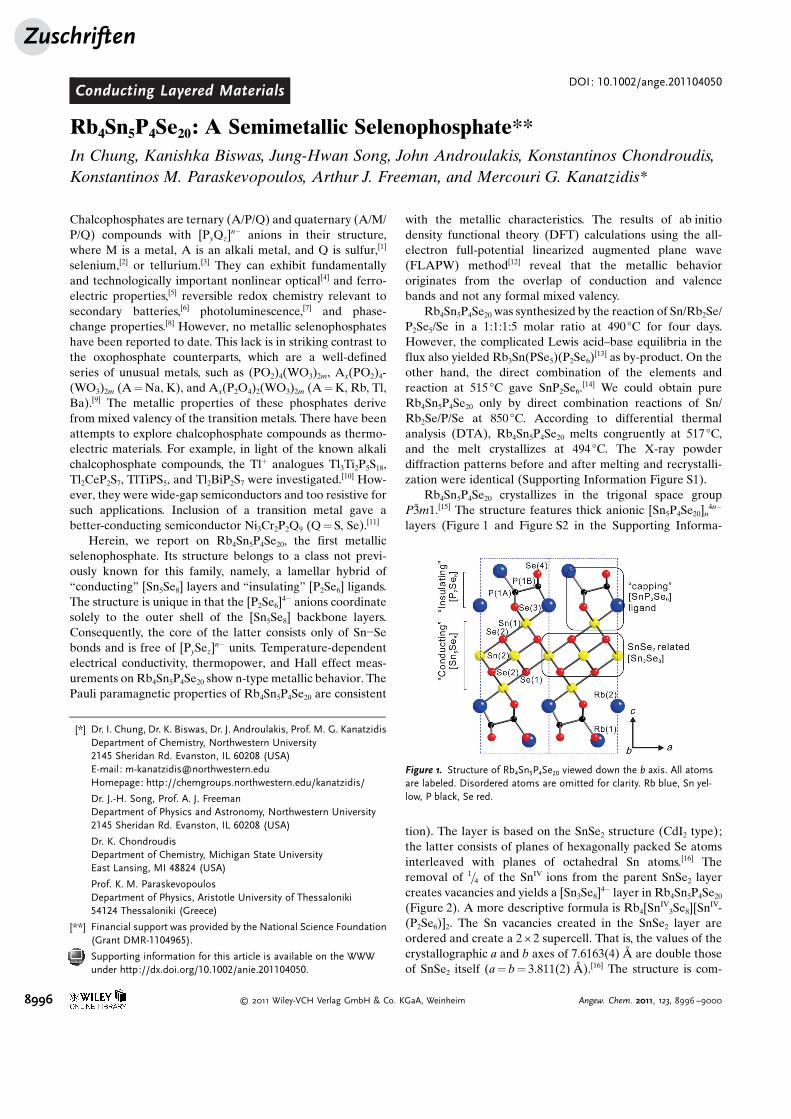
tion). The layer is based on the SnSe2 structure (CdI2 type);the latter consists of planes of hexagonally packed Se atomsinterleaved with planes of octahedral Sn atoms.[16] Theremoval of 1=4 of the SnIV ions from the parent SnSe2 layercreates vacancies and yields a [Sn3Se8]
4� layer in Rb4Sn5P4Se20
(Figure 2). A more descriptive formula is Rb4[SnIV3Se8][SnIV-
(P2Se6)]2. The Sn vacancies created in the SnSe2 layer areordered and create a 2 � 2 supercell. That is, the values of thecrystallographic a and b axes of 7.6163(4) � are double thoseof SnSe2 itself (a = b = 3.811(2) �).[16] The structure is com-
Figure 1. Structure of Rb4Sn5P4Se20 viewed down the b axis. All atomsare labeled. Disordered atoms are omitted for clarity. Rb blue, Sn yel-low, P black, Se red.
[*] Dr. I. Chung, Dr. K. Biswas, Dr. J. Androulakis, Prof. M. G. KanatzidisDepartment of Chemistry, Northwestern University2145 Sheridan Rd. Evanston, IL 60208 (USA)E-mail: [email protected]: http://chemgroups.northwestern.edu/kanatzidis/
Dr. J.-H. Song, Prof. A. J. FreemanDepartment of Physics and Astronomy, Northwestern University2145 Sheridan Rd. Evanston, IL 60208 (USA)
Dr. K. ChondroudisDepartment of Chemistry, Michigan State UniversityEast Lansing, MI 48824 (USA)
Prof. K. M. ParaskevopoulosDepartment of Physics, Aristotle University of Thessaloniki54124 Thessaloniki (Greece)
[**] Financial support was provided by the National Science Foundation(Grant DMR-1104965).
Supporting information for this article is available on the WWWunder http://dx.doi.org/10.1002/anie.201104050.
Zuschriften
8996 � 2011 Wiley-VCH Verlag GmbH & Co. KGaA, Weinheim Angew. Chem. 2011, 123, 8996 –9000
pleted by “capping” of the [Sn3Se8] layer by two [SnP2Se6]fragments from opposite sides in an alternating arrangement.The SnP2Se6 fragments are located at the Sn vacancy points ofthe Sn3Se8 layers (Figure 1).
The two crystallographically unique Sn atoms are stabi-lized in a regular octahedral geometry. The Sn(1) atoms bondto three Se(3) atoms of the tridentate [P2Se6]
4� anions andthree neighboring Se(2) atoms of the [Sn3Se8]
4� slabs(Figure 1), consequently connecting [Sn3Se8]
4� and [SnP2Se6]units to form anionic [Sn5P4Se20]n
4n� layers. The Sn(2) atomscoordinate to two Se(1) and four Se(2) atoms to form the[Sn3Se8] units. The Sn�Se separations are Sn(1)�Se(2)2.6992(8) �, Sn(2)�Se(1) 2.7119(6) �, and Sn(2)�Se(2)2.6972(5) �, comparable to those found in SnSe2 (2.682 �).The [Sn5P4Se20]n
4n� anionic layers are separated by twocrystallographically independent Rb+ cations; the Rb(1) andRb(2) atoms are coordinated by twelve and eight Se atoms,respectively. The Rb�Se distances of the former range from3.20(2) to 3.47(1) � and those for the latter from 3.337(8) to3.55(2) �.
The [P2Se6]4� anions reside on the fixed-symmetry ele-
ments that they do not possess, that is, on the special positionof the P3̄m1 space group: (1/3, 2/3, z), Wyckoff position 2d,site symmetry 3m. They adopt three different orientations bypositional disorder, and therefore, P atoms are one-thirdoccupied (Figure S3 in the Supporting Information). Asimilar symmetry-related disorder is found in Cs10P8Se20,
[17]
K10Sn3(P2Se6)4,[18] and [Mo2Cl8]
n�.[19] Selected area electrondiffraction patterns obtained by transmission electron mi-croscopy and investigation of the reciprocal lattice usingextended X-ray exposure did not reveal any superstructure ortwinning (Figure S4 in the Supporting Information). Wefurther confirm the correctness of crystal structure withdisorder models by examining crystal structure in lowersymmetry of the triclinic and monoclinic space group, forexample, P1̄ and C2/m (subgroup of P3̄m1). We could stillobserve similar disorder behaviors, including positional dis-order of the [P2Se6]
4� units. Introducing additional availablesymmetry elements gave the space group P3̄m1 from thespace groups P1̄ and C2/m and led to an improved R1 value.
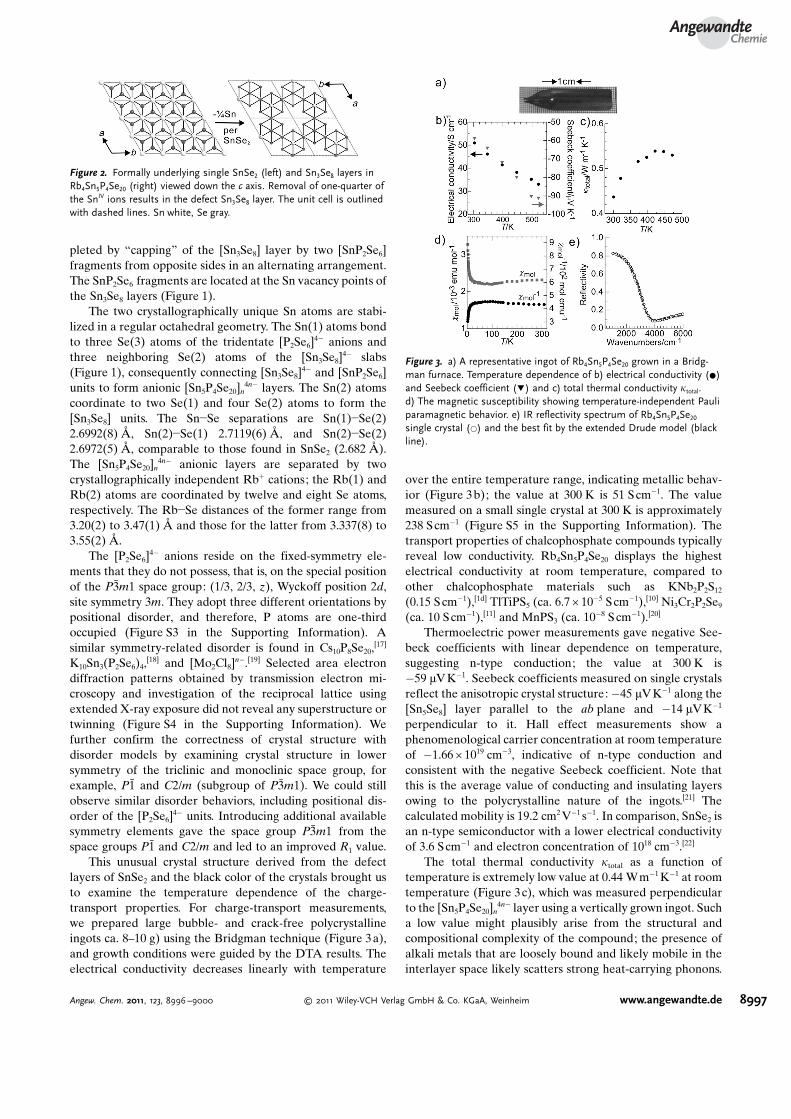
This unusual crystal structure derived from the defectlayers of SnSe2 and the black color of the crystals brought usto examine the temperature dependence of the charge-transport properties. For charge-transport measurements,we prepared large bubble- and crack-free polycrystallineingots ca. 8–10 g) using the Bridgman technique (Figure 3a),and growth conditions were guided by the DTA results. Theelectrical conductivity decreases linearly with temperature
over the entire temperature range, indicating metallic behav-ior (Figure 3b); the value at 300 K is 51 Scm�1. The valuemeasured on a small single crystal at 300 K is approximately238 Scm�1 (Figure S5 in the Supporting Information). Thetransport properties of chalcophosphate compounds typicallyreveal low conductivity. Rb4Sn5P4Se20 displays the highestelectrical conductivity at room temperature, compared toother chalcophosphate materials such as KNb2P2S12
(0.15 S cm�1),[1d] TlTiPS5 (ca. 6.7 � 10�5 Scm�1),[10] Ni3Cr2P2Se9
(ca. 10 Scm�1),[11] and MnPS3 (ca. 10�8 S cm�1).[20]
Thermoelectric power measurements gave negative See-beck coefficients with linear dependence on temperature,suggesting n-type conduction; the value at 300 K is�59 mV K�1. Seebeck coefficients measured on single crystalsreflect the anisotropic crystal structure: �45 mV K�1 along the[Sn5Se8] layer parallel to the ab plane and �14 mVK�1
perpendicular to it. Hall effect measurements show aphenomenological carrier concentration at room temperatureof �1.66 � 1019 cm�3, indicative of n-type conduction andconsistent with the negative Seebeck coefficient. Note thatthis is the average value of conducting and insulating layersowing to the polycrystalline nature of the ingots.[21] Thecalculated mobility is 19.2 cm2 V�1 s�1. In comparison, SnSe2 isan n-type semiconductor with a lower electrical conductivityof 3.6 Scm�1 and electron concentration of 1018 cm�3.[22]
The total thermal conductivity ktotal as a function oftemperature is extremely low value at 0.44 Wm�1 K�1 at roomtemperature (Figure 3c), which was measured perpendicularto the [Sn5P4Se20]n
4n� layer using a vertically grown ingot. Sucha low value might plausibly arise from the structural andcompositional complexity of the compound; the presence ofalkali metals that are loosely bound and likely mobile in theinterlayer space likely scatters strong heat-carrying phonons.
Figure 2. Formally underlying single SnSe2 (left) and Sn3Se8 layers inRb4Sn5P4Se20 (right) viewed down the c axis. Removal of one-quarter ofthe SnIV ions results in the defect Sn3Se8 layer. The unit cell is outlinedwith dashed lines. Sn white, Se gray.
Figure 3. a) A representative ingot of Rb4Sn5P4Se20 grown in a Bridg-man furnace. Temperature dependence of b) electrical conductivity (*)and Seebeck coefficient (!) and c) total thermal conductivity ktotal.d) The magnetic susceptibility showing temperature-independent Pauliparamagnetic behavior. e) IR reflectivity spectrum of Rb4Sn5P4Se20
single crystal (*) and the best fit by the extended Drude model (blackline).
AngewandteChemie
8997Angew. Chem. 2011, 123, 8996 –9000 � 2011 Wiley-VCH Verlag GmbH & Co. KGaA, Weinheim www.angewandte.de
The value of ktotal increases slightly with temperature, asobserved previously in some metal chalcogenide thermo-electric materials containing alkali metals such asA1+xM4�2xM’7+xSe15 (A = K, Rb; M = Pb, Sn; M’= Bi, Sb)[23]
and KBi6.33S10.[24] The value of ktotal is the sum of the phonon
(lattice vibrations) and electronic contribution. The electronicthermal conductivity ke was calculated using the Wiedemann–Franz law ke = LsT, assuming the Lorentz number Lo = 2.44 �10�8 WWK�2. Then, the lattice conductivity klat was calculatedby subtracting the electronic component from ktotal. (Figure S6in the Supporting Information). The result showed that ktotal isdominated by klat. The heat capacity at room temperature is0.19 J g�1 K�1, and it increases with temperature monoto-nously (Figure S4 in the Supporting Information).
Molar magnetic susceptibility measurements ofRb4Sn5P4Se20 indicate temperature-independent, Pauli para-magnetic behavior (Figure 3d) consistent with metallicbehavior. This observation is agreement with the charge-transport results. The “Curie tail” observed at low temper-ature often results from a trace of paramagnetic impurities inthe sample. The data were corrected for ion core diamagnet-ism[25] of�1.13 � 10�3 emumol�1 and were fitted to a modifiedCurie–Weiss law [Eq. (1)]:
cm ¼ c0 þC
T � qð1Þ
where cm is the molar susceptibility, c0 is the temperature-independent Pauli paramagnetic susceptibility, C is the Curieconstant, and q is the critical temperature. The best-fitparameters are c0 = 2.21 � 10�3 emumol�1, C = 2.41 �10�3 emumol�1, and q = 0.41 K. The value of the effectivemagnetic moment mexp = 0.43 mB was calculated from the Cvalue of the fit, thus suggesting the formation of an itinerantspin system typical of metallic compounds.
Infrared reflectivity spectra were collected on singlecrystals in the 1000–6000 cm�1 spectral region at roomtemperature with a resolution of 2 cm�1 (Figure 3e). Theminimum in reflectivity at approximately 3600 cm�1 is typicalof a metallic system. The data were fitted by the equation ofthe extended Drude model for the complex dielectric function~e [Eq. (2)]:[26]
~e wð Þ ¼ e1 1�W2P þ i gP � g0ð Þw
w w� ig0ð Þ
� �ð2Þ
WP is the plasma frequency, gP the carrier damping constant atthe frequency w = WP, g0 the damping value at w = 0, and e1the high-frequency permittivity. The application of this modelfits well to the data with the fitting parameters of e1= 7.1,Wp = 3420 cm�1, gp = 1154 cm�1 and g0 = 670 cm�1. The lowvalue of e1 is indicative of strongly damped phononoscillations, consistent with the low thermal conductivityobserved. The physical meaning of the double-damped Drudemodel is that the carrier damping is not constant butfrequency-dependent [Eq. (3)]:[26]
g wð Þ ¼ g0 þ gP � g0ð Þ w2
W2P
ð3Þ
The mobility mopt at w = WP, the DC optical conductivity s(0)at w = 0, and the free carrier�s effective mass m* werecalculated to be mopt = 451 cm2 V�1 s�1, s(0) = 2059 W�1 cm�1
and m*/m0 = 0.018 by the relations in Equations (4) and (5):
mopt ¼e
m*gPs 0ð Þ ¼ e1W2
P
g0
ð4Þ
N ¼ W2Pm*e1 ð5Þ
The values of mopt, s(0), and N clearly establish thatRb4Sn5P4Se20 is semimetallic. The far-IR spectrum displaysabsorptions at 513, 488, 417, 301, and 213 cm�1, which arecharacteristic of the [P2Se6]
4� group.[27] Absorptions at 234and 181 cm�1 account for Sn�Se vibrations.[28]
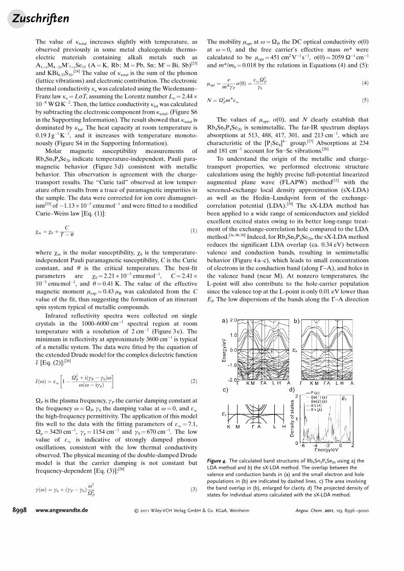
To understand the origin of the metallic and charge-transport properties, we performed electronic structurecalculations using the highly precise full-potential linearizedaugmented plane wave (FLAPW) method[12] with thescreened-exchange local density approximation (sX-LDA)as well as the Hedin–Lundqvist form of the exchange-correlation potential (LDA).[29] The sX-LDA method hasbeen applied to a wide range of semiconductors and yieldedexcellent excited states owing to its better long-range treat-ment of the exchange-correlation hole compared to the LDAmethod.[3a, 4b, 30] Indeed, for Rb4Sn5P4Se20, the sX-LDA methodreduces the significant LDA overlap (ca. 0.34 eV) betweenvalence and conduction bands, resulting in semimetallicbehavior (Figure 4a–c), which leads to small concentrationsof electrons in the conduction band (along G–A), and holes inthe valence band (near M). At nonzero temperatures, theL-point will also contribute to the hole-carrier populationsince the valence top at the L-point is only 0.01 eV lower thanEF. The low dispersions of the bands along the G–A direction
Figure 4. The calculated band structures of Rb4Sn5P4Se20 using a) theLDA method and b) the sX-LDA method. The overlap between thevalence and conduction bands in (a) and the small electron and holepopulations in (b) are indicated by dashed lines. c) The area involvingthe band overlap in (b), enlarged for clarity. d) The projected density ofstates for individual atoms calculated with the sX-LDA method.
Zuschriften
8998 www.angewandte.de � 2011 Wiley-VCH Verlag GmbH & Co. KGaA, Weinheim Angew. Chem. 2011, 123, 8996 –9000
originate from the two-dimensional characteristics of thestructure. The n-type transport behavior discussed abovesuggests that the electrons are much more dominant intransport than the holes.
The angular-momentum-resolved density of states (DOS)for the different atom types in Figure 4d reveals that the low-energy states (�6 to �3 eV) are derived from the strongcovalent interactions among P, Sn, and Se p orbitals. Thepredominant Se p orbitals in the higher-energy states (valenceband maximum (VBM) ca. �3 eV) can be attributed to theirlone-pair states. However, the strong ionic bonding betweenSe(2) and Rb atoms contributes exclusively to the valence-band top (�1 eV to VBM). The strong antibonding statesbetween Sn s and Se p orbitals form a relatively stronglydispersed conduction-band bottom, which leads to the semi-metal characteristics in the compound. At room temperature,it is envisioned that the transport properties are dominated byelectrons of high mobilities, that is, the in-plane largedispersion of the bottom conduction bands.
The discovery of Rb4Sn5P4Se20 reflects the rich structuralchemistry of Sn with [PyQz]
n� chalcophosphate ligands. Thecompound incorporates SnSe2-derived building blocks with[P2Se6]
4� ligands to form a unique low-dimensional structure.Its key element is the metallic character, which is attributed tothe “conducting” [Sn5Se8] layers. This behavior arises fromoverlap of conduction and valence bands in this formallyvalence-precise compound. In addition to the high electricalconductivity, Rb4Sn5P4Se20 shows extremely low thermalconductivity. This finding implies that a large family ofchalcophosphate compounds could be developed for thermo-electric investigations, which have been so far excluded forsuch a purpose because of typical high resistivity. Investiga-tion of new compounds with crystal structures related toRb4Sn5P4Se20 would give more insight into how to circumventsuch a problem.
Received: June 13, 2011Published online: August 2, 2011
.Keywords: conducting materials ·density functional calculations · layered compounds ·selenophosphates · thermoelectric properties
[1] a) M. G. Kanatzidis, Curr. Opin. Solid State & Mater. Sci. 1997, 2,139 – 149; Mater. Sci. 1997, 2, 139 – 149; b) Y. D. Wu, W. Bensch,Inorg. Chem. 2007, 46, 6170 – 6177; c) T. Komm, T. Schleid,J. Solid State Chem. 2005, 178, 454 – 463; d) C. Gieck, V,Derstroff, T. Block, C. Felser, G. Regelsky, O. Jepsen, V.Ksenofontov, P. G�tlich, H. Eckert, W. Tremel, Chem. Eur. J.2004, 10, 382; e) C. Gieck, F. Rocker, V. Ksenofontov, P. Gutlich,W. Tremel, Angew. Chem. 2001, 113, 946 – 948; Angew. Chem.Int. Ed. 2001, 40, 908 – 911; f) J. Sayettat, L. M. Bull, J. C. P.Gabriel, S. Jobic, F. Camerel, A. M. Marie, M. Fourmigue, P.Batail, R. Brec, R. L. Inglebert, Angew. Chem. 1998, 110, 1773 –1776; Angew. Chem. Int. Ed. 1998, 37, 1711 – 1714.
[2] a) C. Rotter, M. Schuster, S. Gebler, T. M. Klapotke, K.Karaghiosoff, Inorg. Chem. 2010, 49, 3937 – 3941; b) C. D.Morris, M. G. Kanatzidis, Inorg. Chem. 2010, 49, 9049 – 9054;c) A. Rothenberger, C. Morris, H. H. Wang, D. Y. Chung, M. G.Kanatzidis, Inorg. Chem. 2009, 48, 9036 – 9040; d) B. C. Chan,
R. F. Hess, P. L. Feng, K. D. Abney, P. K. Dorhout, Inorg. Chem.2005, 44, 2106 – 2113; e) K. Chondroudis. T. J. McCarthy, M. G.Kanatzidis, Inorg. Chem. , 1996, 35, 840 – 844.
[3] a) I. Chung, J. H. Song, M. G. Kim, C. D. Malliakas, A. L. Karst,A. J. Freeman, D. P. Weliky, M. G. Kanatzidis, J. Am. Chem. Soc.2009, 131, 16303 – 16312; b) S. Jçrgens, D. Johrendt, A. Mewis,Chem. Eur. J. 2003, 9, 2405 – 2410.
[4] a) I. Chung, J. I. Jang, C. D. Malliakas, J. B. Ketterson, M. G.Kanatzidis, J. Am. Chem. Soc. 2010, 132, 384 – 389; b) I. Chung,J. H. Song, J. I. Jang, A. J. Freeman, J. B. Ketterson, M. G.Kanatzidis, J. Am. Chem. Soc. 2009, 131, 2647 – 2656; c) I.Chung, J. I. Jang, M. A. Gave, D. P. Weliky, M. G. Kanatzidis,Chem. Commun. 2007, 4998 – 5000; d) I. Chung, C. D. Malliakas,J. I. Jang, C. G. Canlas, D. P. Weliky, M. G. Kanatzidis, J. Am.Chem. Soc. 2007, 129, 14996 – 15006; e) P. G. Lacroix, R.Clement, K. Nakatani, J. Zyss, I. Ledoux, Science 1994, 263,658 – 660.
[5] a) X. Bourdon, A. R. Grimmer, V. B. Cajipe, Chem. Mater. 1999,11, 2680 – 2686; b) B. Scott, M. Pressprich, R. D. Willet, D. A.Cleary, J. Solid State Chem. 1992, 96, 294 – 300.
[6] a) Y. Kim, N. Arumugam, J. B. Goodenough, Chem. Mater. 2008,20, 470 – 474; b) A. H. Thompson, M. S. Whittingham, US Pat.,1977, 4049879.
[7] a) S. Banerjee, J. M. Szarko, B. D. Yuhas, C. D. Malliakas, L. X.Chen, M. G. Kanatzidis, J. Am. Chem. Soc. 2010, 132, 5348 –5350; b) Y. D. Wu, W. Bensch, Inorg. Chem. 2008, 47, 7523 –7534; c) S. Banerjee, C. D. Malliakas, J. I. Jang, J. B. Ketterson,M. G. Kanatzidis, J. Am. Chem. Soc. 2008, 130, 12270 – 12272;d) G. Gauthier, S. Jobic, F. Boucher, P. Macaudiere, D. Hugue-nin, J. Rouxel, R. Brec, Chem. Mater. 1998, 10, 2341 – 2347.
[8] a) I. Chung, J. Do, C. G. Canlas, D. P. Weliky, M. G. Kanatzidis,Inorg. Chem. 2004, 43, 2762 – 2764; b) J. D. Breshears, M. G.Kanatzidis, J. Am. Chem. Soc. 2000, 122, 7839 – 7840.
[9] M. Greenblatt, Acc. Chem. Res. 1996, 29, 219 – 228.[10] M. A. McGuire, T. K. Reynolds, F. J. DiSalvo, Chem. Mater.
2005, 17, 2875 – 2884.[11] M. A. McGuire, F. J. DiSalvo, Chem. Mater. 2007, 19, 4600 –
4605.[12] E. Wimmer, H. Krakauer, M. Weinert, A. J. Freeman, Phys. Rev.
B 1981, 24, 864 – 875.[13] K. Chondroudis, M. G. Kanatzidis, J. Solid State Chem. 1998, 136,
79 – 86.[14] C. D. Carpentier, R. Nitsche, Mater. Res. Bull. 1974, 9, 1097 –
1100.[15] Crystal data for Rb4Sn5P4Se20 at 173(2) K: Siemens SMART
Platform CCD diffractometer, Mo Ka radiation (l = 0.71073 �),trigonal, P3̄m1, a = b = 7.6163(4), c = 18.690(1) �, V=
938.91(9) �3, Z = 1; Mr = 2638.41 gmol�1; Dcalc = 4.666 gcm�3,Dexp = 4.64 gcm�3, m = 27.989 mm�1, 2qmax = 56.568, 6157 totalreflections, 952 unique reflections with Rint = 4.17%, GOF =
1.137, 60 parameters, R1 = 3.40%, wR2 = 8.91% for I> 2s(I),largest diff. peak and hole 1.264 and �2.391 e��3. Furtherdetails of the crystal structure investigations may be obtainedfrom the Fachinformationszentrum Karlsruhe, 76344 Eggen-stein-Leopoldshafen, Germany (fax: (+ 49)7247 – 808 – 666;e-mail: [email protected]) on quoting the depositionnumber CSD-422904.
[16] G. Busch, C. Frçhlich, F. Hulliger, E. Steigmeier, Helv. Chim.Acta 1961, 34, 359 – 368.
[17] I. Chung, D. Holmes, D. P. Weliky, M. G. Kanatzidis, Inorg.Chem. 2010, 49, 3092 – 3094.
[18] I. Chung, M. G. Kanatzidis, Inorg. Chem. 2011, 50, 412 – 414.[19] F. A. Cotton, J. L. Eglin, Inorg. Chim. Acta 1992, 198 – 200, 13 –
22.[20] P. A. Joy, S. Vasudevan, J. Am. Chem. Soc. 1992, 114, 7792 – 7801.[21] C. M. Hurd, The Hall effect in metals and alloys, Plenum Press,
New York, 1972.
AngewandteChemie
8999Angew. Chem. 2011, 123, 8996 –9000 � 2011 Wiley-VCH Verlag GmbH & Co. KGaA, Weinheim www.angewandte.de
[22] G. Domingo, R. S. Itoga, C. Kannewurf, Phys. Rev. 1966, 143,536 – 541.
[23] K. S. Choi, D. Y. Chung, A. Mrotzek, P. Brazis, C. R. Kannewurf,C. Uher, W. Chen, T. Hogan, M. G. Kanatzidis, Chem. Mater.2001, 13, 756 – 764.
[24] M. G. Kanatzidis, T. J. McCarthy, T. A. Tanzer, L. H. Chen, L.Iordanidis, T. Hogan, C. R. Kannewurf, C. Uher, B. X. Chen,Chem. Mater. 1996, 8, 1465 – 1474.
[25] L. N. Mulay, Magnetic susceptibility, John Wiley & Sons, Inc.,New York, 1963.
[26] F. Gervais, in Infrared and Millimeter Waves, Vol. 8 (Ed.: K. J.Button), Academic, New York, 1983, p. 306.
[27] G. Kliche, J. Solid State Chem. 1984, 51, 118 – 126.[28] J. Y. Harbec, S. Jandl, Phys. Rev. B 1982, 25, 6126 – 6129.[29] L. Hedin, B. I. Lundqvist, J. Phys. C 1971, 4, 2064 – 2083.[30] a) R. Asahi, W. Mannstadt, A. J. Freeman, Phys. Rev. B 1999, 59,
7486 – 7492; b) T. K. Bera, J. H. Song, A. J. Freeman, J. I. Jang,J. B. Ketterson, M. G. Kanatzidis, Angew. Chem. 2008, 120,7946 – 7950; Angew. Chem. Int. Ed. 2008, 47, 7828 – 7832; c) J. H.Song, A. J. Freeman, T. K. Bera, I. Chung, M. G. Kanatzidis,Phys. Rev. B 2009, 79, 245203.
Zuschriften
9000 www.angewandte.de � 2011 Wiley-VCH Verlag GmbH & Co. KGaA, Weinheim Angew. Chem. 2011, 123, 8996 –9000