Embed Size (px)
Citation preview
A Rapid, Non-Contact Method for Measurement of Si Wafer Thickness: Principles and Preliminary Results Preprint
August 2003 • NREL/CP-520-34654
B. Sopori, C. Auriemma, C. Li, and J. Madjdpour To be presented at the 13th Workshop on Crystalline Silicon Solar Cell Materials and Processes Vail, Colorado August 10-13, 2003
National Renewable Energy Laboratory 1617 Cole Boulevard Golden, Colorado 80401-3393 NREL is a U.S. Department of Energy Laboratory Operated by Midwest Research Institute • Battelle • Bechtel
Contract No. DE-AC36-99-GO10337
NOTICE
The submitted manuscript has been offered by an employee of the Midwest Research Institute (MRI), a contractor of the US Government under Contract No. DE-AC36-99GO10337. Accordingly, the US Government and MRI retain a nonexclusive royalty-free license to publish or reproduce the published form of this contribution, or allow others to do so, for US Government purposes.
This report was prepared as an account of work sponsored by an agency of the United States government. Neither the United States government nor any agency thereof, nor any of their employees, makes any warranty, express or implied, or assumes any legal liability or responsibility for the accuracy, completeness, or usefulness of any information, apparatus, product, or process disclosed, or represents that its use would not infringe privately owned rights. Reference herein to any specific commercial product, process, or service by trade name, trademark, manufacturer, or otherwise does not necessarily constitute or imply its endorsement, recommendation, or favoring by the United States government or any agency thereof. The views and opinions of authors expressed herein do not necessarily state or reflect those of the United States government or any agency thereof.
Available electronically at http://www.osti.gov/bridge
Available for a processing fee to U.S. Department of Energy and its contractors, in paper, from:
U.S. Department of Energy Office of Scientific and Technical Information P.O. Box 62 Oak Ridge, TN 37831-0062 phone: 865.576.8401 fax: 865.576.5728 email: [email protected]
Available for sale to the public, in paper, from:
U.S. Department of Commerce National Technical Information Service 5285 Port Royal Road Springfield, VA 22161 phone: 800.553.6847 fax: 703.605.6900 email: [email protected] online ordering: http://www.ntis.gov/ordering.htm
Printed on paper containing at least 50% wastepaper, including 20% postconsumer waste
A Rapid, Non-contact Method for Measurement of Si Wafer Thickness: Principles and Preliminary Results
Bhushan Sopori, Chris Auriemma, Chuan Li, and Jamal Madjdpour
National Renewable Energy Laboratory 1617 Cole Blvd.
Golden, CO 80401
INTRODUCTION The thickness of a semiconductor wafer can critically influence mechanical and/or electronic yield of the device(s) fabricated on it. For most microelectronic (surface) devices, the thickness of a wafer is important primarily for mechanical reasons—to provide control and stability of devices by minimizing stresses resulting from various device-fabrication processes. However, for minority-carrier devices, such as solar cells, the entire thickness of the wafer participates in the optical and electronic performance of the device. In either case, control of wafer thickness through careful measurement is a fundamental requirement in the commercial fabrication of electronic devices. In the microelectronics industry, the thickness of a wafer is controlled through various steps involving wafering, etching, and polishing, which typically produce flat wafers with parallel surfaces. The thickness of such a wafer is well defined, and its measurement is somewhat straightforward. A variety of methods have been used in the semiconductor industry for wafer-thickness measurement. Two of the most common are:
• Dial gauge — a manual, mechanical measurement, generally used in the laboratory for a small number of wafers. • Impedance method — which measures capacitance or eddy current loss in an rf bridge configuration.
The microelectronics industry uses almost exclusively non-contact, impedance methods for wafer-thickness measurements. These techniques take a few seconds for each wafer, but require knowledge of the resistivity of the wafers. However, they are not well suited for mapping the thickness variations. The solar industry imposes very severe demands on a technique for wafer-thickness measurement because of the following reasons:
• Large throughput —Even a small commercial production facility deals with a large number of wafers (e.g., a typical manufacturing facility may use 50,000 wafers/day). Of these, a reasonable fraction must be measured for meaningful QA purposes. Concomitantly, measurement technique must be very rapid. • Wafers are not typically flat —in particular, Si ribbons deviate strongly from non-parallel surfaces and have surfaces that exhibit strong variations in the surface morphology. Here, one must measure some kind of “average” thickness and/or determine a thickness profile.
1
• Wafers can be single-crystalline as well as multi(or poly)-crystalline— the impedance method can produce inaccuracies for multi- or polycrystalline wafers because of the extraneous impedance associated with grain boundaries and defects. • Wafers have rough surfaces — Solar cells require rough or textured surfaces to lower surface reflectance and maximize optical absorption. This leads to inaccuracies in most measurement methods. Surface roughness is particularly detrimental for optical techniques. Another form of surface roughness can occur because of morphological problems arising from improper sawing.
The demands of solar industry are difficult to meet. The difficulties are further intensified by a need for minimizing the equipment and the measurement costs. The solar cell industry typically uses wafer weighing as a method for monitoring wafer thickness. Some companies (that use single-crystal wafers) employ impedance-based methods to measure thickness of a very small number of total wafers. Thus, solar industry needs a method for measurement of wafer thickness that can yield meaningful results for wafers that may have rough and/or non-parallel surfaces. Such a method should be rapid, accurate, and low cost. We describe a new method for measuring wafer thickness. This is a non-contact, optical method that can determine an average value of the thickness of the entire wafer in a very short time (< 100 ms). It is applicable to wafers of all surface morphologies (polished, rough, textured) and lends itself readily for making maps of the wafer thickness.
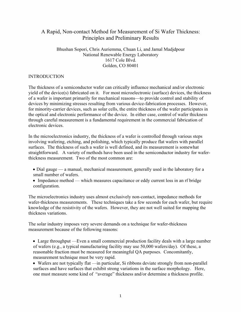
PRINCIPLES OF THE NEW METHOD In this method, the measurement parameter is the total reflectance spectrum of the test wafer. The measured reflectance (or preselected segments of it) is compared with a database of spectra generated by calculation or through measurements made on calibrated samples. This database includes reflectance spectra for wafers of different thickness and surface characteristics. The calculations are performed using PV Optics [1, 2]. Because the surface properties of the test wafer are known, the comparison yields the thickness of the wafer. The total reflectance spectrum of the test wafer is measured by Sopori reflectometer (licensed to GTi, which offers this instrument for sale as GT-Fabscan ). The measured reflectance spectrum carries information pertaining to thickness of the wafer as well as properties of its surfaces. It should be pointed out that surface properties of the test wafer are generally known before the desired measurement proceeds. The approach described here is applicable to any wafer (of any surface quality and thickness variation), but we will consider specific cases only—cases that are of interest to the solar or semiconductor industry. To understand the principle of the proposed technique, we first consider reflectance of a double-sided, parallel polished Si wafer (see Figure 1). Consider a wafer of thickness (t), illuminated by a beam of light. The total reflectance (RT) and total transmittance (TT) can be written as:
R R R e
R eT
t
t= +−−
−
−1 11
2 2
2 2( ) α
α
( )T
R eR eT
t
t=− ⋅−
−
−
11
2
2
α
α
where
2
R n k
n k=
− ++ +
( )( )
11
2 2
2 2 and T t ktr = − = −exp( ) exp( / )α π λ4
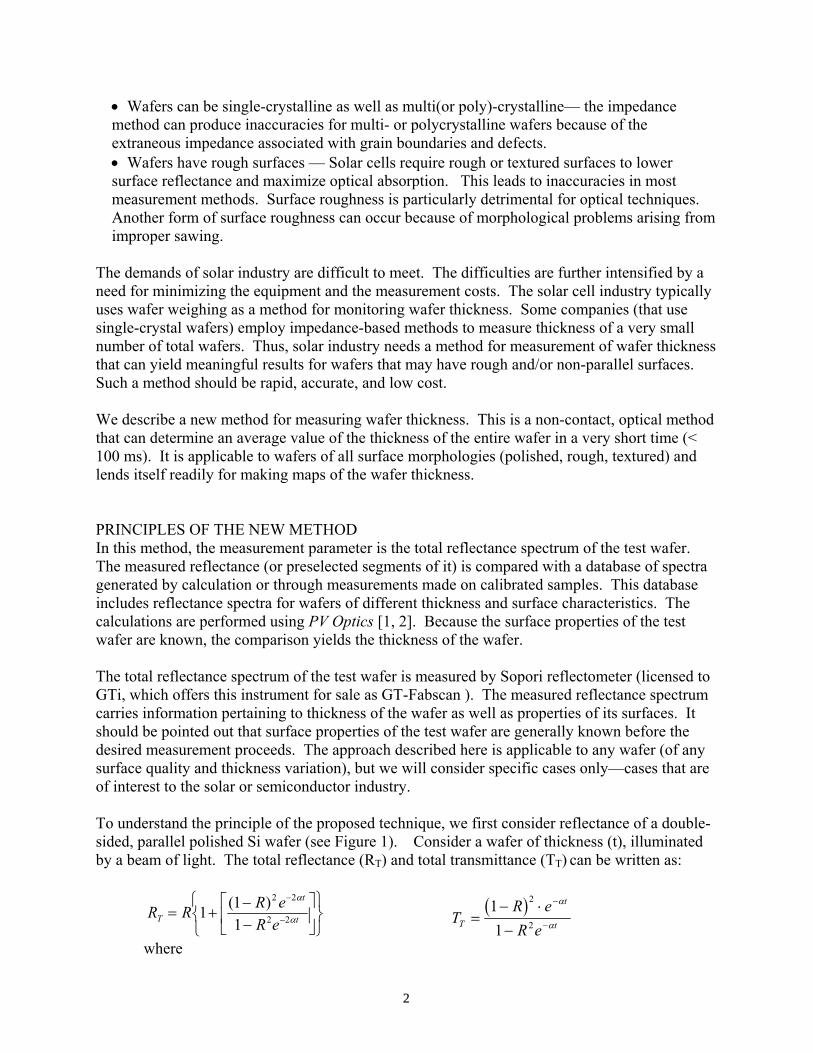
Here, n, k, and α are the refractive index, extinction coefficient, and absorption coefficient, respectively. Figure 2 is a plot of RT for two samples, 50 µm and 300 µm in thickness. The RT Vs λ can be divided into three regions. Region I corresponds to the high-absorption region; here the reflectance is simply from the front side of the wafer. In Region II, the absorption coefficient is moderate and the reflectance has contributions from the front as well as the back side (including multiplereflections from within the wafer itself). In this region, the thicker wafer has lower reflectance for a selected value of λ. Region III is weakly absorbing. Concomitantly, reflectance is almost independent of the wafer thickness. Thus, region II is of primary interest for the measurement of wafer thickness.
Figure 2. Calculated reflectance spectra of 50-µm (dotted) and 300-µm thick (solid) Si wafers.
Incident light
(1-R)e-αt
R
(1-R)
Figure 1. Illustration of total reflectance and transmittance of a semiconductor wafer.
Region I
3
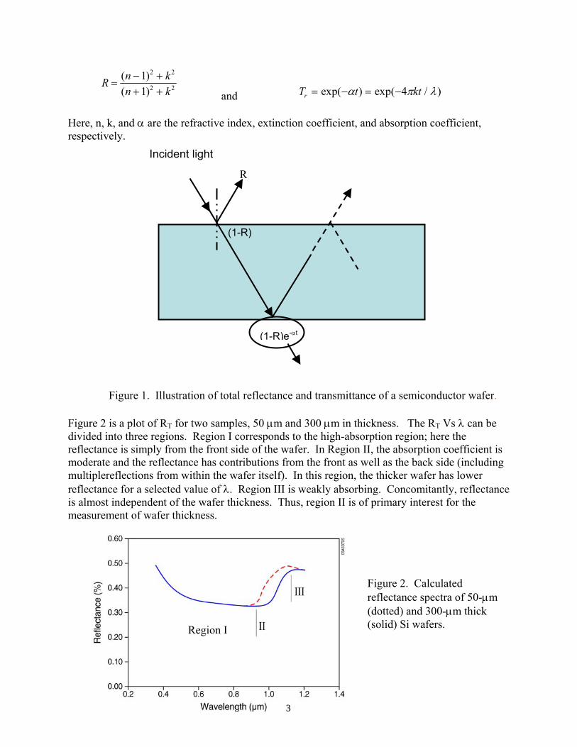
A similar RT Vs λ can also be determined for unpolished wafers. Figure 3 shows calculated reflectance spectra of two double-side-textured wafers, one 50 µm thick and the other 300 µm thick. The reflectance spectra exhibit characteristics similar to those of Figure 2, with the following variations: 1. The reflectance in Region I is much lower (about 10%). 2. The reflectance in the Region III is also lower than in the corresponding region of Fig. 2. 3. We see in both cases (Figs. 2 and 3) that there is a large separation between the curves of thin
and thick wafers in Region II. There are several approaches of using this region for measuring wafer thickness.
APPROACHES TO DECONVOLVE RT VS λ CURVE Because the reflectance spectrum of a wafer carries information that relates to the surfaces as well as the wafer thickness, it is important to develop a systematic approach to deconvolve the spectrum. As indicated, the reflectance of a Si wafer in the highly absorbing region is characteristic mainly of the surface morphology. Hence, Region I of the spectrum can be used to identify the nature of the front surface. A polished wafer exhibits the highest reflectance. A rough surface has lower reflectance, and periodic roughness can further lower the reflectance. If the surface characteristics and the thickness of a wafer are known, the entire reflectance spectrum can be calculated using PV Optics. Conversely, if the reflectance spectrum of a wafer
Figure 3. Calculated reflectance spectra of double-side-textured wafers that are 50 µm thick (dotted) and 300 µm thick (solid).
4
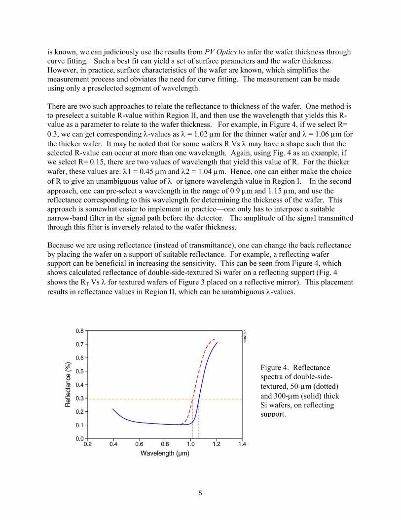
is known, we can judiciously use the results from PV Optics to infer the wafer thickness through curve fitting. Such a best fit can yield a set of surface parameters and the wafer thickness. However, in practice, surface characteristics of the wafer are known, which simplifies the measurement process and obviates the need for curve fitting. The measurement can be made using only a preselected segment of wavelength. There are two such approaches to relate the reflectance to thickness of the wafer. One method is to preselect a suitable R-value within Region II, and then use the wavelength that yields this R-value as a parameter to relate to the wafer thickness. For example, in Figure 4, if we select R= 0.3, we can get corresponding λ-values as λ = 1.02 µm for the thinner wafer and λ = 1.06 µm for the thicker wafer. It may be noted that for some wafers R Vs λ may have a shape such that the selected R-value can occur at more than one wavelength. Again, using Fig. 4 as an example, if we select R= 0.15, there are two values of wavelength that yield this value of R. For the thicker wafer, these values are: λ1 = 0.45 µm and λ2 = 1.04 µm. Hence, one can either make the choice of R to give an unambiguous value of λ or ignore wavelength value in Region I. In the second approach, one can pre-select a wavelength in the range of 0.9 µm and 1.15 µm, and use the reflectance corresponding to this wavelength for determining the thickness of the wafer. This approach is somewhat easier to implement in practice—one only has to interpose a suitable narrow-band filter in the signal path before the detector. The amplitude of the signal transmitted through this filter is inversely related to the wafer thickness. Because we are using reflectance (instead of transmittance), one can change the back reflectance by placing the wafer on a support of suitable reflectance. For example, a reflecting wafer support can be beneficial in increasing the sensitivity. This can be seen from Figure 4, which shows calculated reflectance of double-side-textured Si wafer on a reflecting support (Fig. 4 shows the RT Vs λ for textured wafers of Figure 3 placed on a reflective mirror). This placement results in reflectance values in Region II, which can be unambiguous λ-values.
Figure 4. Reflectance spectra of double-side-textured, 50-µm (dotted) and 300-µm (solid) thick Si wafers, on reflecting support.
5
AVERAGE THICKNESS The proposed technique relies on the changes in the optical absorption due to change in the wafer thickness. Hence, the measured thickness is “averaged” over the area of illumination. If the entire wafer is illuminated, this technique inherently averages the thickness of the wafer because it measures the reflectance of the entire wafer. This feature of the proposed method is very valuable for solar industry. The solar industry uses a variety of different types of wafers, and some of these include ribbons. The ribbons are not flat wafers but they taper away from the middle of the wafer. In these cases, the thickness monitoring requires an average thickness of the wafer. METHOD AND SOME RESULTS This method consists of measuring RT Vs λ of the entire wafer in a GT-FabScan [3,4]. This instrument rapidly measures the wavelength dependence of reflectance of the entire wafer (or cell), up to 6-in x 6-in in size. These data are analyzed to derive parameters related to surface roughness and texture, antireflection coatings, front-metallization properties (area fraction and thickness), and the back-contact properties of a solar cell. The GT-FabScan operates according to the concept of “reciprocal optics” — in which the sample is illuminated through a very wide angle of incidence and the normal component of the reflected light is measured. We point out that one approach for implementing this concept is to use an integrating sphere to randomize the direction of the light before it impinges on the test sample. However, the integrating-sphere approach is not suitable for large-area measurements. The approach used in the GT-FabScan is unique—it uses multiple, wide-angle, light sources to illuminate the large-area sample, and the light scattered normal to the sample is collected for analysis. This new approach makes the system quite simple, low cost, and rapid, and it permits use of high-power sources to enable measurement of “optically averaged” parameter values for large-area solar cells and wafers. However, because only the light reflected in a direction normal to the sample must be collected, this approach demands that all the extraneous light must be excluded. Such extraneous light includes non-normal components of the light reflected from the test wafer, as well as the scattered light from parts of the instrument such as the wafer holder and mounting brackets. To accomplish this, the GT-FabScan uses highly absorbing surfaces and a system of light-trapping baffles, resulting in an extremely high S/N ratio (of about 200). This allows the entire measurement and analysis to be made in less than 10 s, which can be further reduced to less than 1 s. Here we present some results showing the repeatability of measuring the reflectance spectra and the sensitivity of the spectra to wafer thickness. These results are given in Figures 5-8. Excellent repeatability and thickness sensitivity of better than 20 µm can be observed.
6
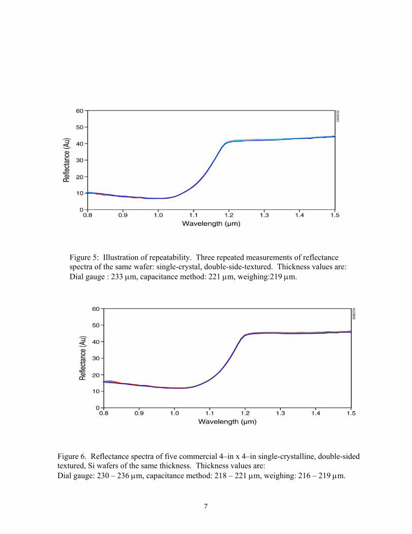
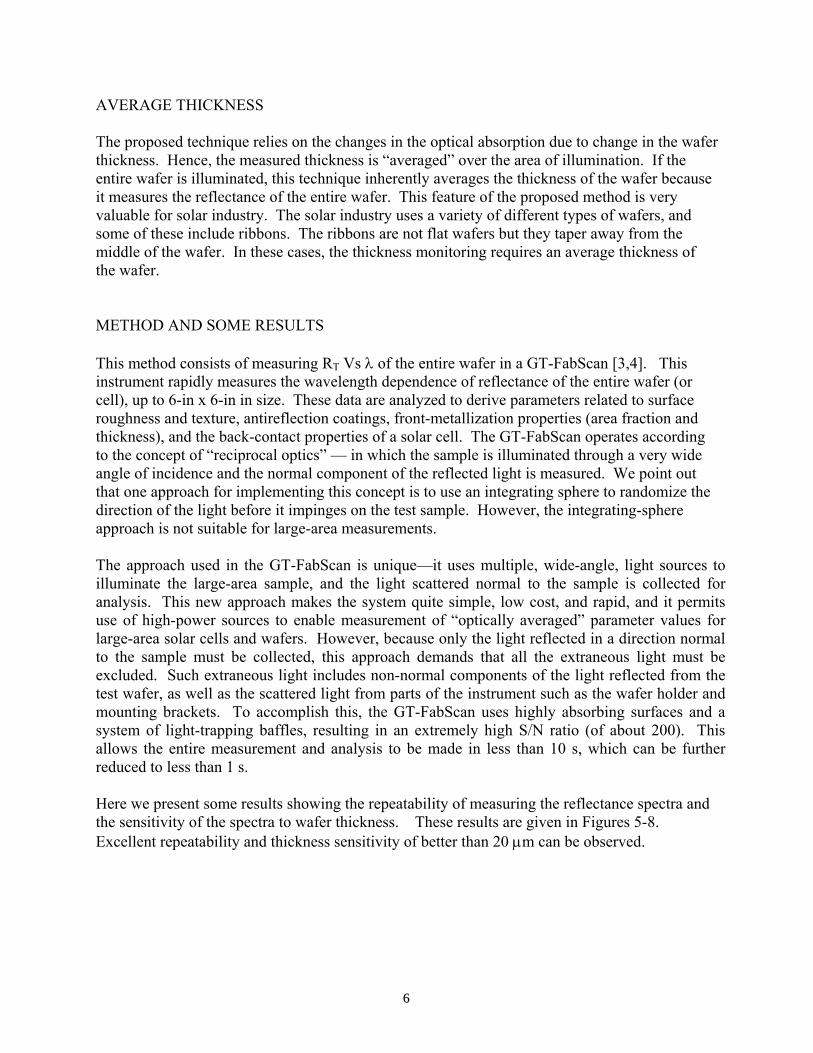
Figure 5: Illustration of repeatability. Three repeated measurements of reflectance spectra of the same wafer: single-crystal, double-side-textured. Thickness values are:Dial gauge : 233 µm, capacitance method: 221 µm, weighing:219 µm.
Figure 6. Reflectance spectra of five commercial 4–in x 4–in single-crystalline, double-sided textured, Si wafers of the same thickness. Thickness values are: Dial gauge: 230 – 236 µm, capacitance method: 218 – 221 µm, weighing: 216 – 219 µm.
7
Figure 7b. Measured reflectance spectra of two mc-Si wafers 150-µm (dotted) and 260-µm (solid) thick.
Figure 7a. Calculated reflectance spectra of two mc-Si wafers 150-µm (dotted) and 260-µm (solid) thick.
8
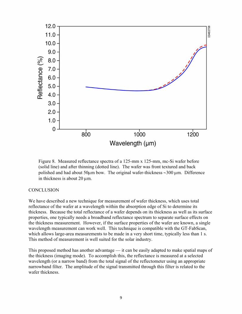
CONCLUSION We have described a new technique for measurement of wafer thickness, which uses total reflectance of the wafer at a wavelength within the absorption edge of Si to determine its thickness. Because the total reflectance of a wafer depends on its thickness as well as its surface properties, one typically needs a broadband reflectance spectrum to separate surface effects on the thickness measurement. However, if the surface properties of the wafer are known, a single wavelength measurement can work well. This technique is compatible with the GT-FabScan, which allows large-area measurements to be made in a very short time, typically less than 1 s. This method of measurement is well suited for the solar industry. This proposed method has another advantage — it can be easily adapted to make spatial maps of the thickness (imaging mode). To accomplish this, the reflectance is measured at a selected wavelength (or a narrow band) from the total signal of the reflectometer using an appropriate narrowband filter. The amplitude of the signal transmitted through this filter is related to the wafer thickness.
Figure 8. Measured reflectance spectra of a 125-mm x 125-mm, mc-Si wafer before (solid line) and after thinning (dotted line). The wafer was front textured and back polished and had about 50µm bow. The original wafer-thickness ∼300 µm. Difference in thickness is about 20 µm.
9
In other measurements, we have made some preliminary comparisons between the thickness measured by this technique and other techniques consisting of dial gauge, wafer weighing, and capacitance method. These results show an excellent agreement. ACKNOWLEDGEMENT This work was supported by the US Department of Energy under contract #DE-AC36-99G010337 REFERENCES [1]. B. L. Sopori, Laser Focus, 34, 159 (Feb. 1998). [2]. B. L. Sopori and T. Marshall, Procd. 23rd IEEE Photovoltaic Specialists Conference, 1993 (New York: IEEE). [3] B. L. Sopori, “Principle of a new reflectometer for measuring dielectric film thickness on substrates of arbitrary characteristics,” Rev. Sci. Instrum. 59(5), 725, 1988. [4] Proc. 9th Workshop on Crystalline Silicon Solar Cell Materials and Processing, pp 74-80, August 9-11, 1999, Breckenridge, CO.
10
REPORT DOCUMENTATION PAGE
Form Approved OMB NO. 0704-0188
Public reporting burden for this collection of information is estimated to average 1 hour per response, including the time for reviewing instructions, searching existing data sources, gathering and maintaining the data needed, and completing and reviewing the collection of information. Send comments regarding this burden estimate or any other aspect of this collection of information, including suggestions for reducing this burden, to Washington Headquarters Services, Directorate for Information Operations and Reports, 1215 Jefferson Davis Highway, Suite 1204, Arlington, VA 22202-4302, and to the Office of Management and Budget, Paperwork Reduction Project (0704-0188), Washington, DC 20503. 1. AGENCY USE ONLY (Leave blank)
2. REPORT DATE
August 2003
3. REPORT TYPE AND DATES COVERED
Conference Paper
4. TITLE AND SUBTITLE A Rapid, Non-Contact Method for Measurement of Si Wafer Thickness: Principles and
Preliminary Results; Preprint 6. AUTHOR(S) B. Sopori, C. Auriemma, C. Li, and J. Madjdpour
5. FUNDING NUMBERS
PVP33101
7. PERFORMING ORGANIZATION NAME(S) AND ADDRESS(ES) National Renewable Energy Laboratory 1617 Cole Blvd. Golden, CO 80401-3393
8. PERFORMING ORGANIZATION
REPORT NUMBER NREL/CP-520-34654
9. SPONSORING/MONITORING AGENCY NAME(S) AND ADDRESS(ES)
10. SPONSORING/MONITORING
AGENCY REPORT NUMBER
11. SUPPLEMENTARY NOTES 12a. DISTRIBUTION/AVAILABILITY STATEMENT
National Technical Information Service U.S. Department of Commerce 5285 Port Royal Road
Springfield, VA 22161
12b. DISTRIBUTION CODE
13. ABSTRACT (Maximum 200 words): The thickness of a semiconductor wafer can critically influence mechanical and/or electronic yield of the device(s) fabricated on it. For most microelectronic (surface) devices, the thickness of a wafer is important primarily for mechanical reasons—to provide control and stability of devices by minimizing stresses resulting from various device-fabrication processes. However, for minority-carrier devices, such as solar cells, the entire thickness of the wafer participates in the optical and electronic performance of the device. In either case, control of wafer thickness through careful measurement is a fundamental requirement in the commercial fabrication of electronic devices.
15. NUMBER OF PAGES
14. SUBJECT TERMS: photovoltaics; Si wafer thickness; non-contact method; device; solar cell; commercial fabrication; minority carrier;
16. PRICE CODE
17. SECURITY CLASSIFICATION
OF REPORT Unclassified
18. SECURITY CLASSIFICATION
OF THIS PAGE Unclassified
19. SECURITY CLASSIFICATION
OF ABSTRACT Unclassified
20. LIMITATION OF ABSTRACT
UL
NSN 7540-01-280-5500 Standard Form 298 (Rev. 2-89) Prescribed by ANSI Std. Z39-18 298-102