Embed Size (px)
Citation preview
RESEARCH NEWS
February 200512
Carbon nanotube (CNT)-based polymer
composites could offer high electrical
conductivity and advantageous
mechanical properties. Working toward
this goal, scientists at the University of
Cambridge and Imperial College in the
UK and Hamburg Institute of
Technology in Germany have dispersed
multiwalled nanotubes in an epoxy
system based on a bisphenol-A resin
and an amine hardener (Martin et al.,
Polymer (2005) 46, 877).
A shear-intensive mechanical stirring
process provides excellent dispersion
of the CNTs in the epoxy component.
Applying ac and dc electric fields
during nanocomposite curing results in
the formation of aligned, conductive
nanotube networks. The networks were
evaluated by in situ optical microscopy
and current density measurements for
different electric field strengths and
nanotube weight fractions.
Electric-field-induced forces acting on
the CNTs, which have a negative
surface charge after processing in the
epoxy, dominate nanotube
agglomeration. Networks formed in
ac fields are more uniform and better
aligned those obtained in dc fields.
Increased field strength improves
uniformity and alignment of the
networks as well as enhancing bulk
conductivity of the composite material.
However, the maximum specific
composite conductivity that can be
achieved using this approach is still
low compared to the conductivity value
of multiwalled CNTs alone. This
indicates the presence of polymer
barriers that prevent direct contact
between individual nanotubes.
The researchers believe their approach
shows promise for creating conductive
nanotube-polymer composites with
anisotropic electrical properties. John K. Borchardt
Electric-fieldaligned CNTcompositesCOMPOSITES
Polymers containing photocrosslinkable groups arebeing developed for macro- and microlithography,liquid crystal displays, nonlinear optical materials,photocurable coatings, and energy exchangematerials. Ultraviolet (UV) irradiation crosslinks thepolymers selectively in the illuminated regions, butrapid curing in the radiated areas is essential.While some industrial applications have alreadybeen commercialized, more rapid curing rates aredesirable. Polymers with chalcone in the backboneor side chain undergo rapid crosslinking uponirradiation with UV light. However, the preparationand evaluation of photocrosslinkable acrylamidepolymers bearing chalcone as a pendant group hasnot been reported.Now, researchers at Anna University in Chennai,India have synthesized acrylamide monomers thatcould provide significantly more rapid curing ratesthan currently achievable (Selvam and Nanjundan,Reactive Funct. Polym. (2005) 62, 179). Themonomers, 4-acrylamidophenyl-2’,3’-benzostyrylketone (APBSK) and 4-acrylamidophenyl-4’-N,N’-dimethylstyryl ketone (APDSK), have a free-radicalpolymerizable group and a photocrosslinkable
functional group. Polymerization is performed at70°C using benzoyl peroxide as the free radicalinitiator and methyl ethyl ketone as the solvent. Thermogravimetric analysis in air of the resultingpolymers indicates that they have sufficient thermaland thermo-oxidative stability to be used as negativephotoresists, with poly(APBSK) being more stablethan poly(APDSK). Photosensitivity was investigatedin various solvents in the presence and absence oftriplet photosensitizers. Rapid photocrosslinking ofpoly(APBSK) appears to be caused by the presenceof an electron donating group (NCH3). The bulkynaphthyl group present in poly(APDSK) appears tosterically hinder the approach of the pendant groupsfor photocoupling, reducing photocrosslinking rates.In the absence of triplet sensitizers, this reactionrate depends on the solvent, concentration, andsubstituent in the pendant chalcone moiety.Because the pendant chalcone unit possesses highphotosensitivity, even in the absence of a tripletphotosensitizer, poly(APBSK) and poly(APDSK) wouldbe useful as negative photoresists for variousapplications.John K. Borchardt
Rapid crosslinking in acrylamide polymersPOLYMERS
Light-processable photonic crystalsOPTICAL MATERIALS
Photonic crystals can be used to control theemission of light and could enable a newgeneration of optical devices of reduced size.Self-assembly of monodisperse spheres intoordered three-dimensional opal structures isone way of making large-area photoniccrystal films of controlled thickness. Using a surfactant-free emulsion
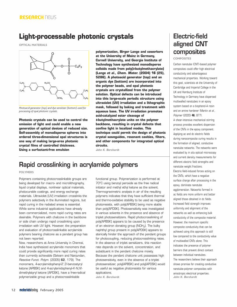
polymerization, Birger Lange and coworkersat the University of Mainz in Germany,Cornell University, and Georgia Institute ofTechnology have synthesized monodispersecolloids made from poly(t-butylmethacrylate)(Lange et al., Chem. Mater. (2004) 16 (25),5286). A photoacid generator (top) and anorganic dye (bottom) are incorporated intothe polymer beads, and opal photoniccrystals are crystallized from the polymersolution. Optical defects can be introducedinto this large-scale periodic structure usingultraviolet (UV) irradiation and a lithographicmask, followed by baking and treatment withaqueous base. The UV irradiation promotesacid-catalyzed ester cleavage of t-butylmethacrylate units on the polymerbackbone, resulting in crystal defects thatconfine light in localized modes. Thistechnique could permit the design of photoniccrystal waveguides, resonant cavities, filters,and other components for integrated opticalcircuits. John K. Borchardt
Photoacid generator (top) and dye sensitizer (bottom) used for
processing of opal photonic crystals.
![Synthesis and Characterization of Graft Co-Polymers of ... · Grafting of butylacrylate, acrylic acid [16] and acrylonitrile onto starch, acrylamide onto natural fiber and butyl methacrylate](https://img.pdfslide.us/doc/110x75/5ec2ad19914f582a603bc313/synthesis-and-characterization-of-graft-co-polymers-of-grafting-of-butylacrylate.jpg)


![Photochemical Crosslinking for Tailoring Properties of Polymers · 3.3.2 Photochemical crosslinking ... Homopolymer synthesis for endo,exo-bicyclo[2.2.1]hept-5-ene-2,3-dicarboxylic](https://img.pdfslide.us/doc/110x75/61321fd0dfd10f4dd73a3ec3/photochemical-crosslinking-for-tailoring-properties-of-polymers-332-photochemical.jpg)