Embed Size (px)
Citation preview
RAPID ASSEMBLY OF MULTILAYER MICROFLUIDIC STRUCTURES
C. Glick, A. Schwartz, M. Srimongkol, J. Lin, W. Zhuang R. Warren, D. Tekell, P. Satamalee, and L. Lin
University of California, Berkeley, USA
ABSTRACTWe demonstrate rapid 3D-printed molding and
assembly of two-sided PDMS devices. Advancing the 3D printed transfer molding technique from single-sided microfluidics to multi-layer microfluidic manufacturing, this work utilizes the ease of 3D printing to create complementary molds with built-in alignment structures to PDMS layers and then assemble them at the end. Using this single-step double-sided molding method, we demonstrate the molding of complex geometries in PDMS – including vias, built-in alignment marks, and membrane valves – that are difficult or impossible to achieve using standard soft lithography. The membrane valves show distinctive transistor characteristic curves and a closing pressure of 200 kPa. A new stamp-bonding method is used to selectively apply liquid PDMS adhesive, demonstrating a reliable method of assembling multi-layered PDMS microfluidic devices.
INTRODUCTIONMicrofluidic Fabrication via Soft Lithography
Microfluidic devices for manipulating fluids have rapidly advanced since the 1980s due to their unique ability to make low-cost, high-throughput platforms, particularly for chemical and biological research and Lab-on-a-Chip technologies [1,2]. The most far-reaching breakthrough inmicrofluidics has been the development of soft-lithography - using rigid micromachined molds to shape elastomeric polymers [3]. Among polymers, Poly(dimethylsiloxane) (PDMS) is commonly used due to its numerous ideal properties, including ease of manufacturing and reasonable cost, as well as its strength, transparency, and especially biocompatibility [4].
One method of increasing geometric complexity is ‘multilevel soft lithography’ [6], where the channels are non-planar and/or rounded [7]. Although rounded channels would be beneficial for some microfluidic applications, few groups have developed appropriate fabrication
techniques [8-10] because multilevel soft lithography has historically required multiple photolithography steps [11-16]. While multilayer PDMS manufacturing techniques have been demonstrated by several groups [17,18], these are even more time-consuming and labor-intensive, requiring multiple lithography steps as well as precision alignment, issues which are only partially addressed by dedicated PDMS alignment apparatuses [19].
Microfluidic Fabrication via 3D Printing3D printing has presented a unique route for building
multilevel and multilayer microfluidic devices directly, or indirectly via molding processes. For example, various groups have used 3D printers previously to make simple microfluidic devices with truly 3D geometries, including microfluidic devices without moving elements, such as resistors [20] and modular components [21], as well as those with movable components, such as capacitors, diodes and transistors [22]. Currently, 3D printed microfluidics is limited by: (i) the available resolution of the printer [20]; (ii) surface roughness of the printed material and support layers [23,24]; and (iii) material types [25, 26]; however, 3D printing technologies are expected to rapidly advance and address these limitations.
Although direct 3D printing is a rapid process for prototyping, for making multiple copies of microfluidic devices, 3D printed transfer molding (PTM), remains faster, cheaper, and more reliable. First pioneered by McDonald et al. using fused deposition modeling techniques [27], the technique has since been used with stereolithography [28], multijet printing [23], as well as with wax printers [29] and office-quality laserjet printers [30,31]. While PTM does not allow the same geometric flexibility of fully 3D printed microfluidics, it possesses three notable advantages: (i) reusability, (ii) better device resolution, and (iii) compatibility with existing PDMS device fabrication techniques [27,32-35].
Figure 1: Conceptual diagram illustrating rapid assembly of multilayer PDMS microfluidic devices. (a) 3D printed stamp is used to selectively
non-channel areas of the device allowing bonding of two complementary layers of PDMS without clogging. (b) Diagram illustrating overlapping fluid flow achievable by bonding multiple layers of PDMS. (c) PDMS layer with corresponding stamp.
Figure 2: Rapid assembly of six-layer PDMS microfluidic device with double-sided transfer molding and stamp bonding. (a) Six component PDMS layers. (b) Assembled device showing fluid mixing: downward helices (blue and yellow) mix and return in upward helix (green).
978-1-5386-4782-0/18/$31.00 ©2018 IEEE 1241 MEMS 2018, Belfast, Northern Ireland, UK, 21-25 January 2018
CONCEPTWhile double-sided PDMS molding can be completed
with spin-bonding to glass [34], fully multilayer microfluidic devices (created by 3D printed molding or conventional soft lithography) require a PDMS-PDMS bonding step [35]. For 3D molded PDMS components, we have developed 3D printed stamps to selectively apply PDMS as a more consistent bonding technique, as shown in Figure 1a. The stamps can easily be designed and printed from the original CAD drawings, to selectively apply uncured liquid PDMS ( ) only to non-channel areas of the PDMS component. These stamps (Figure 1c) may contain features that intrude or extrude from the plane of the stamp, which allow the stamp to be used on numerous
ing, multi-layered microfluidic devices are easily assembled, allowing fluid flow within or between the various layers (Figure 1b). Additionally, previously discussed techniques (e.g., alignment marks, built-in inlets/outlets, and variable channels) may be used in conjunction with rapid assembly. Including the 40-minutebonding allows a six-layer microfluidic device (Figure 2) to be assembled and bonded in under an hour.
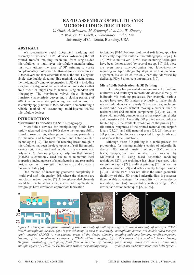
Figure 3 summarizes general fabrication techniques for double-sided 3D printed transfer molding. (a) First, a pair of molds are 3D Printed from a CAD model and fitted using built-in alignment marks. (b) Next, the mold filled with PDMS cured. (c) The PDMS device has built-in inlets/outlets, membranes, and vias, and is (d) bonded to glass to create enclosed, arbitrary channels.
Figure 3: Conceptual illustration of two-sided 3D printed molding techniques. (a) Mold is Printed from CAD model, treated, fitted using alignment marks, and (b) filled with PDMS, cured and the mold is removed. (c) PDMS device contains built-in inlets/outlets, membranes, and vias, and (d) is glass-bonded to create enclosed channels.
EXPERIMENTAL TECHNIQUESMold Preparation
The microfluidic devices were designed and converted from a positive to a negative mold shape using the computer-aided design program SolidWorks. 3D printing of molds was achieved using a Projet 3000 3D printer. During printing, the Projet 3000 deposited layers of structural epoxy (VisiJet® EX200 plastic material) and sacrificial wax (VisiJet® S100 support material); the wax was used as a temporary support for hollow spaces as well as to provide a foundational layer for the mold, and was removed during post-processing. Following printing, the molds were cleaned to remove the sacrificial wax. First, the molds were baked in a VWR 1330 FM oven 75ºC for 45
minutes to melt the sacrificial wax. The molds were then washed in a sequence of three cleaning baths for 10 minutesin each bath to remove leftover wax: warm Bayes mineral oil, Ajax dish detergent in water, and potable water. The molds then dried. After cleaning and drying, the 3D printed molds were treated with an anti-adhesive agent (PFOTSgas) to facilitate the removal of PDMS.
PDMS (Sylgard 184 Elastomer Kit) was prepared using the standard 10:1 as the base:curing agent ratio. The PDMS mixture was degassed in a vacuum chamber for 10 minutes and then poured into the 3D printed molds. The filled molds were then placed in the vacuum chamber for 45 min to degas and increase PDMS conformity. Following the degassing, the molds were baked in an 80 ºC oven for 50 min. The PDMS microfluidic devices were removed from the molds by first cutting away excess PDMS and then by manually peeling the PDMS loose from the mold. The finer the printed features, the more carefully this removal must be performed. Provided no features have broken during the de-molding process and PDMS did not permanently bond to the mold, the molds are reusable without an additional cleaning process.
RESULTS AND DISCUSSIONFabrication Results
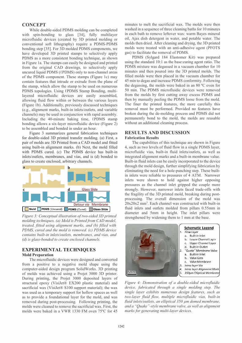
The capabilities of this technique are shown in Figure 4, such as two levels of fluid flow in a single PDMS layer, microfluidic vias, built-in fluid inlets/outlets, as well as integrated alignment marks and a built-in membrane value. Built-in fluid inlets can be easily incorporated to the device through the mold design, further simplifying fabrication by eliminating the need for a hole-punching step. These built-in inlets were reliable to pressures of 4 ATM. Narrower inlets were shown to hold against higher opposing pressures as the channel inlet gripped the couple more strongly. However, narrower inlets faced trade-offs with the fragility of the 3D printed mold, breaking during post-processing. The overall dimension of the mold was 20x20x2 mm3. Each channel was constructed with built-in fluid inlets and outlets molded from pillars 0.55mm in diameter and 5mm in height. The inlet pillars were strengthened by widening them to 1 mm at the base.
Figure 4: Demonstration of a double-sided microfluidic device, fabricated through a single molding step. The single layer exhibits numerous design features, such as two-layer fluid flow, multiple microfluidic vias, built-in fluid inlets/outlets, an elliptical 350 μm domed membrane, and a “Quake”-style membrane valve, as well as alignment marks for generating multi-layer devices.
1242
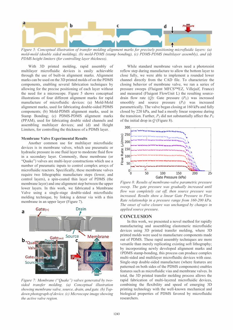
Figure 5: Conceptual illustration of transfer molding alignment marks for precisely positioning microfluidic layers: (a) mold-mold (double sided molding), (b) mold-PDMS (stamp bonding), (c) PDMS-PDMS (multilayer assembly), and (d) PDMS height limiters (for controlling layer thickness).
With 3D printed molding, rapid assembly of multilayer microfluidic devices is easily achievable through the use of built-in alignment marks. Alignment marks can be used on the 3D printed molds of on the PDMS components, enabling several fabrication techniques by allowing for the precise positioning of each layer without the need for a microscope. Figure 5 shows conceptual illustrations of four different alignment marks for rapid manufacture of microfluidic devices: (a) Mold-Mold alignment marks, used for fabricating double-sided PDMS components; (b) Mold-PDMS alignment marks, used in Stamp Bonding; (c) PDMS-PDMS alignment marks (PPAM), used for fabricating double sided channels and assembling multilayer devices; and (d) and Height Limiters, for controlling the thickness of a PDMS layer.
Membrane Valve Experimental ResultsAnother common use for multilayer microfluidic
devices is in membrane valves, which use pneumatic or hydraulic pressure in one fluid layer to moderate fluid flow in a secondary layer. Commonly, these membrane (or “Quake”) valves are multi-layer constructions which use a number of pneumatic inputs to control complex arrays of microfluidic reactors. Specifically, these membrane valves require two lithographic manufacture steps (lower, and control layers), a spin-coated thin layer of PDMS (the membrane layer) and one alignment step between the upper lower layers. In this work, we fabricated a Membrane Valve using a single-stage double-sided microfluidic molding technique, by linking a detour via with a thin membrane in an upper layer (Figure 7).
Figure 7: Membrane (“Quake”) valves generated by two-sided transfer molding. (a) Conceptual illustration showing membrane valve, source, drain, and gate. (b) Top-down photograph of device. (c) Microscope image showing the active valve region.
While standard membrane valves need a photoresist reflow step during manufacture to allow the bottom layer to close fully, we were able to implement a rounded lower channel directly from the CAD file. To characterize the closing behavior of membrane valve, we ran a series of pressure sweeps (Fluigent MFCS™EZ, Villejuif, France) and measured (Fluigent FlowUnit L) the resulting source-drain flow rate (Q): Gate pressure (PG) was increased smoothly and source pressure (PS) was increased parametrically. The valve began closing at 160 kPa and fully closed by 220 kPa, and had a mostly linear response during the transition. Further, PS did not substantially affect the PGof the initial drop in Q (Figure 8).
Figure 8: Results of membrane-valve parametric pressure sweep. The gate pressure was gradually increased until flow was completely cut off, then source pressure was increased. Results show a linear Gate Pressure to Flow Rate relationship in a pressure range from 160-200 kPa. The onset of valve closure was unchanged by changes in applied source pressure.
CONCLUSIONIn this work, we presented a novel method for rapidly
manufacturing and assembling elastomeric microfluidicdevices using 3D printed transfer molding, where 3D printed molds were used to manufacture components made out of PDMS. These rapid assembly techniques are more versatile than merely replicating existing soft lithography; by incorporating newly developed alignment marks and
-bonding, this process can produce complex multi-sided and multilayer microfluidic devices with ease. Single-step double-sided manufacture (where features are patterned on both sides of the PDMS components) enables features such as microfluidic vias and membrane valves. Intotal, the 3D printed transfer molding process allows the rapid fabrication of multi-layered microfluidic devices,combining the flexibility and speed of emerging 3D printing technology with the well-known mechanical andbiological properties of PDMS favored by microfluidicresearchers.
1243

ACKNOWLEDGEMENTSThe authors thank the members of the Liwei Lin Laboratory and the Micro Mechanical Methods for Biology(M3B) Laboratory Program. This research is supported in part by the DARPA N/MEMS program under the Micro/Nano Fluidics Fundamentals Focus (MF3) center and by the National Science Foundation.
REFERENCES [1] Xia, Y. & Whitesides, G. Soft lithography. Annual
Review Of Materials Science (1998).
[2] Duffy, D., et al. Rapid prototyping of microfluidic systems in poly(dimethylsiloxane). Analytical Chemistry (1998).
[3] Whitesides, G. M., et al. Soft lithography in biologyand biochemistry. Annual review of biomedical engineering (2001).
[4] Kim, P. et al. Soft lithography for microfluidics: a review. BioChip Journal (2008).
[5] Thorsen, T., et al. Microfluidic large-scaleintegration. Science (2002).
[6] LaVan, D. A., et al. Moving smaller in drug discoveryand delivery. Nature Review Drug Discovery (2002).
[7] Chiu, D. T. et al. Patterned deposition of cells and proteins onto surfaces by using three-dimensionalmicrofluidic systems. PNAS (2000).
[8] Wilson, M. E. et al. Fabrication of circularmicrofluidic channels by combining mechanicalmicromilling and soft lithography. Lab Chip (2011).
[9] Abdelgawad, M. et al. A fast and simple method to fabricate circular microchannels in poly-dimethylsiloxane. Lab Chip (2011).
[10] Sochol, R. D. et al. Microfluidic bead-baseddiodes with targeted circular microchannels forlow Reynolds number applications. Lab Chip (2014).
[11] Mata, A., Fleischman, A. J. & Roy, S. Fabrication of multi-layer su-8 microstructures. JMEMS (2006).
[12] Henke, W., et al. Simulation andexperimental studyof gray-tone lithography for the fabrication ofarbitrarily shaped surfaces. MEMS (1994).
[13] Waits, C. M., Modafe, A. & Ghodssi, R. Investigationof gray-scale technology for large area 3D siliconmems structures. JMEMS (2003).
[14] Toepke, M. W., & Kenis, P. J. A. Multilevelmicrofluidics via single-exposure photolithography.Journal of the American Chemical Society (2005).
[15] Seo, K., et al. Fabrication and applications of complex-shaped microparticles via microfluidics. Lab on a Chip (2015).
[16] Loomis, J., et al. Grayscale lithography automatedmask generation for complex three-dimensionaltopography. Journal of Micro/Nanolithography,MEMS, and NEMS (2016).
[17] Gray, B. et al. Novel interconnection technologies for integrated microfluidic systems. SNA-A (1999).
[18] Zhang, M., et al. A simple method for fabricating multi-layer PDMS structures for 3D microfluidic chips. Lab Chip (2010).
[19] Li, X. et al. Desktop aligner for fabrication ofmultilayer microfluidic devices. Review ofScientific Instruments (2015).
[20] Au, A. K., et al. 3D-printed microfluidics. Angewandte Chemie International Edition (2016).
[21] Bhargava, K. C., et al. Discrete elements for 3D microfluidics. PNAS (2014).
[22] Sochol, R. D. et al. 3D printed microfluidic circuitry via multijet-based additive manufacturing. Lab Chip (2016).
[23] Hwang, Y. et al. 3D printed molds for non-planarPDMS microfluidic channels. SNA-A (2015).
[24] Walczak, R. & Adamski, K. Inkjet 3D printing of microfluidic structureson the selection of the printer towards printing your own microfluidic chips. JMEMS (2015).
[25] Yuen, P. K. & Goral, V. N. Low-cost rapid prototyping of flexible microfluidic devices using adesktop digital craft cutter. Lab Chip (2010).
[26] Wu, S., et al. 3D-printed microelectronics forintegrated circuitry and passive wireless sensors. Microsystems & Nanoengineering (2015).
[27] McDonald, J. C. et al. Prototyping of microfluidicdevices in poly(dimethylsiloxane) using solid-objectprinting. Analytical Chemistry (2002).
[28] Comina, G., et al. PDMS lab-on-a-chip fabricationusing 3D printed templates. Lab Chip (2014).
[29] Kaigala, G. V., et al. Rapid prototyping of micro-fluidic devices with a wax printer. Lab Chip (2007).
[30] Lobo Junior, D. E. O. et al. High fidelity prototyping of PDMS electrophoresis microchips using laser-printed masters. Microsystem Technologies (2015).
[31] Thomas, M. S. et al. Print-and-peel fabrication for microfluidics: What’s in it for biomedical applica-tions? Annals of Biomedical Engineering (2009).
[32] Bonyar, A. et al. Characterization of rapid PDMS casting technique utilizing molding forms fabricatedby 3D rapid prototyping technology. InternationalJournal of Material Forming (2014).
[33] Comina, G., et al. 3D printed unibody lab-on-a-chip: Features survey and check- valves integration. Micromachines (2015).
[34] Glick, C.G. et al. Fabrication of Double-Sided Microfluidic Structures via 3D Printed Transfer Molding. Hilton Head (2016).
[35] Glick, C.G. et al. Rapid Assembly of Multilayer Microfluidic Structures via 3D Printed Transfer Molding and bonding. MicroNano (2016).
CONTACT*C. Glick, tel: +1-530-5192324; [email protected]
1244