Embed Size (px)
Citation preview
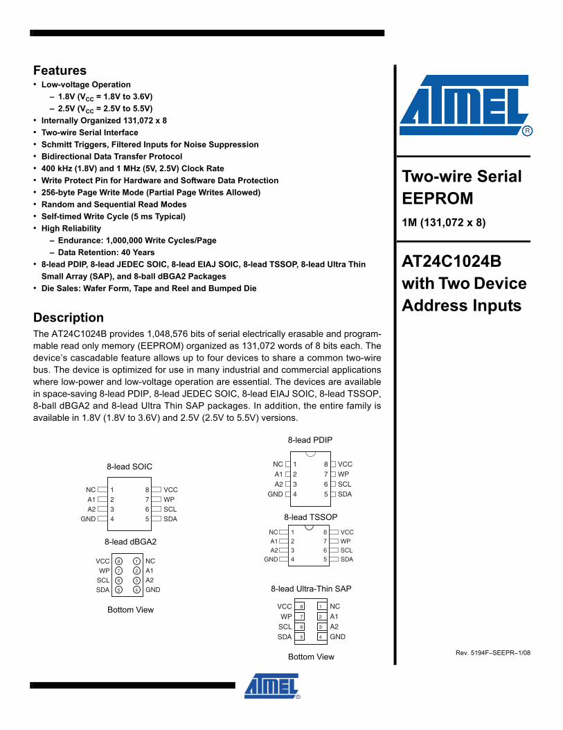
Two-wire Serial EEPROM1M (131,072 x 8)
AT24C1024Bwith Two Device Address Inputs
Rev. 5194F–SEEPR–1/08
Features• Low-voltage Operation
– 1.8V (VCC = 1.8V to 3.6V)– 2.5V (VCC = 2.5V to 5.5V)
• Internally Organized 131,072 x 8• Two-wire Serial Interface• Schmitt Triggers, Filtered Inputs for Noise Suppression• Bidirectional Data Transfer Protocol• 400 kHz (1.8V) and 1 MHz (5V, 2.5V) Clock Rate• Write Protect Pin for Hardware and Software Data Protection• 256-byte Page Write Mode (Partial Page Writes Allowed)• Random and Sequential Read Modes• Self-timed Write Cycle (5 ms Typical)• High Reliability
– Endurance: 1,000,000 Write Cycles/Page– Data Retention: 40 Years
• 8-lead PDIP, 8-lead JEDEC SOIC, 8-lead EIAJ SOIC, 8-lead TSSOP, 8-lead Ultra Thin Small Array (SAP), and 8-ball dBGA2 Packages
• Die Sales: Wafer Form, Tape and Reel and Bumped Die
DescriptionThe AT24C1024B provides 1,048,576 bits of serial electrically erasable and program-mable read only memory (EEPROM) organized as 131,072 words of 8 bits each. Thedevice’s cascadable feature allows up to four devices to share a common two-wirebus. The device is optimized for use in many industrial and commercial applicationswhere low-power and low-voltage operation are essential. The devices are availablein space-saving 8-lead PDIP, 8-lead JEDEC SOIC, 8-lead EIAJ SOIC, 8-lead TSSOP,8-ball dBGA2 and 8-lead Ultra Thin SAP packages. In addition, the entire family isavailable in 1.8V (1.8V to 3.6V) and 2.5V (2.5V to 5.5V) versions.
8-lead PDIP
1234
8765
NCA1A2
GND
VCCWPSCLSDA
8-lead TSSOP
1234
8765
VCCWP SCL SDA
NCA1A2
GND
8-lead SOIC
1234
8765
NCA1A2
GND
VCCWPSCLSDA
8-lead Ultra-Thin SAP
Bottom View
VCC WP
SCL SDA
NCA1A2GND
1
2
3
4
8
7
6
5
8-lead dBGA2
Bottom View
VCC WP
SCL SDA
NCA1A2GND
1
2
3
4
8
7
6
5
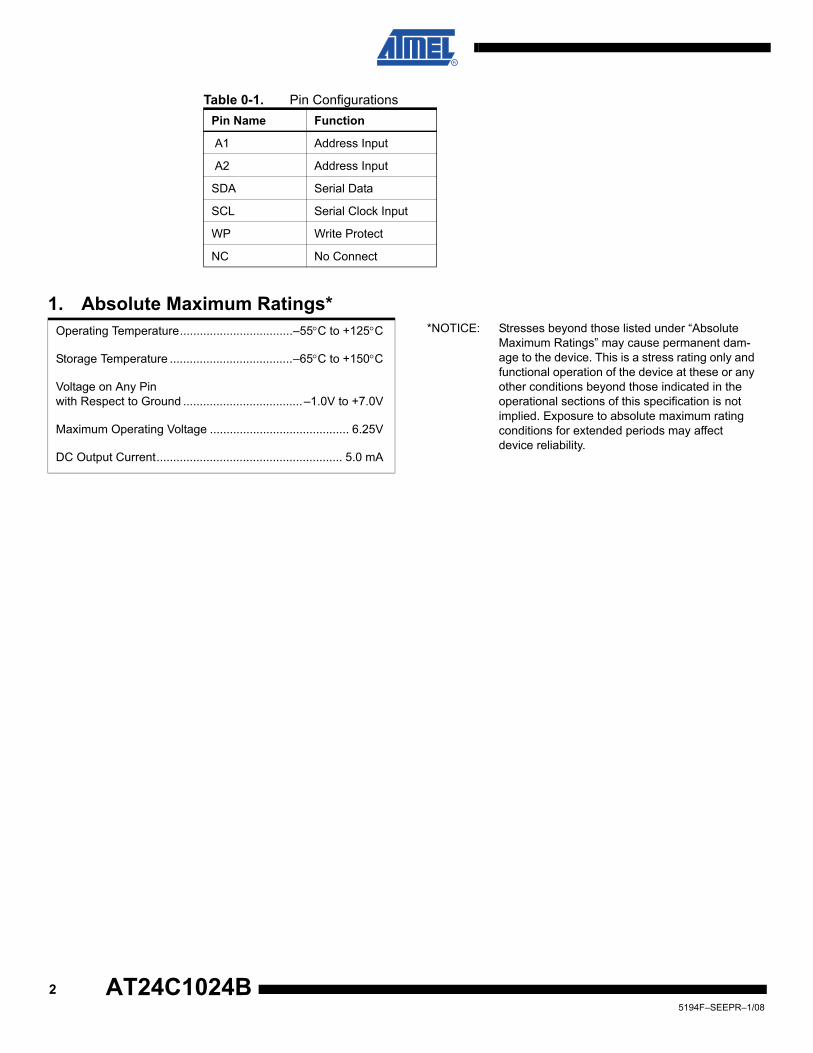
Table 0-1. Pin ConfigurationsPin Name Function
A1 Address Input
A2 Address Input
SDA Serial Data
SCL Serial Clock Input
WP Write Protect
NC No Connect
1. Absolute Maximum Ratings*Operating Temperature..................................–55°C to +125°C *NOTICE: Stresses beyond those listed under “Absolute
Maximum Ratings” may cause permanent dam-age to the device. This is a stress rating only and functional operation of the device at these or any other conditions beyond those indicated in the operational sections of this specification is not implied. Exposure to absolute maximum rating conditions for extended periods may affect device reliability.
Storage Temperature .....................................–65°C to +150°C
Voltage on Any Pinwith Respect to Ground ....................................–1.0V to +7.0V
Maximum Operating Voltage .......................................... 6.25V
DC Output Current........................................................ 5.0 mA
25194F–SEEPR–1/08
AT24C1024B
AT24C1024B
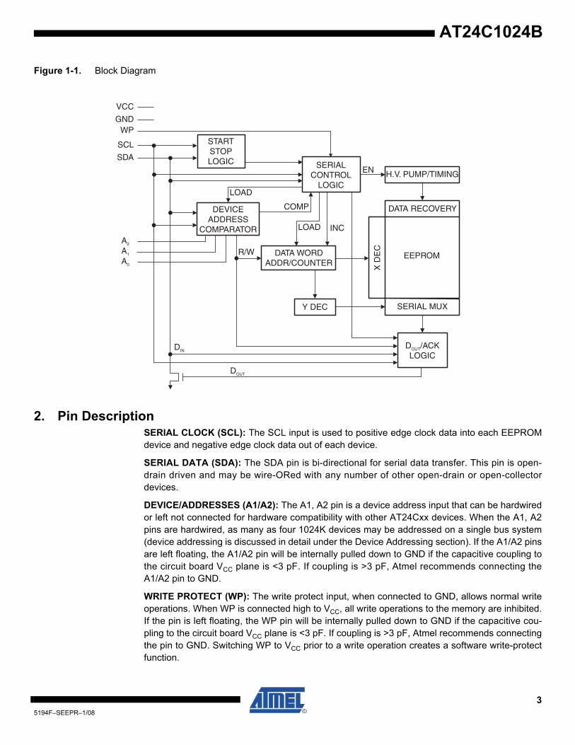
Figure 1-1. Block Diagram
2. Pin DescriptionSERIAL CLOCK (SCL): The SCL input is used to positive edge clock data into each EEPROMdevice and negative edge clock data out of each device.
SERIAL DATA (SDA): The SDA pin is bi-directional for serial data transfer. This pin is open-drain driven and may be wire-ORed with any number of other open-drain or open-collectordevices.
DEVICE/ADDRESSES (A1/A2): The A1, A2 pin is a device address input that can be hardwiredor left not connected for hardware compatibility with other AT24Cxx devices. When the A1, A2pins are hardwired, as many as four 1024K devices may be addressed on a single bus system(device addressing is discussed in detail under the Device Addressing section). If the A1/A2 pinsare left floating, the A1/A2 pin will be internally pulled down to GND if the capacitive coupling tothe circuit board VCC plane is <3 pF. If coupling is >3 pF, Atmel recommends connecting theA1/A2 pin to GND.
WRITE PROTECT (WP): The write protect input, when connected to GND, allows normal writeoperations. When WP is connected high to VCC, all write operations to the memory are inhibited.If the pin is left floating, the WP pin will be internally pulled down to GND if the capacitive cou-pling to the circuit board VCC plane is <3 pF. If coupling is >3 pF, Atmel recommends connectingthe pin to GND. Switching WP to VCC prior to a write operation creates a software write-protectfunction.
STARTSTOPLOGIC
VCC
GNDWP
SCL
SDA
A2
A1
A0
SERIALCONTROL
LOGIC
EN H.V. PUMP/TIMING
EEPROM
DATA RECOVERY
SERIAL MUX
X D
EC
DOUT/ACKLOGIC
COMP
LOAD INC
DATA WORDADDR/COUNTER
Y DEC
R/W
DOUT
DIN
LOAD
DEVICEADDRESS
COMPARATOR
35194F–SEEPR–1/08
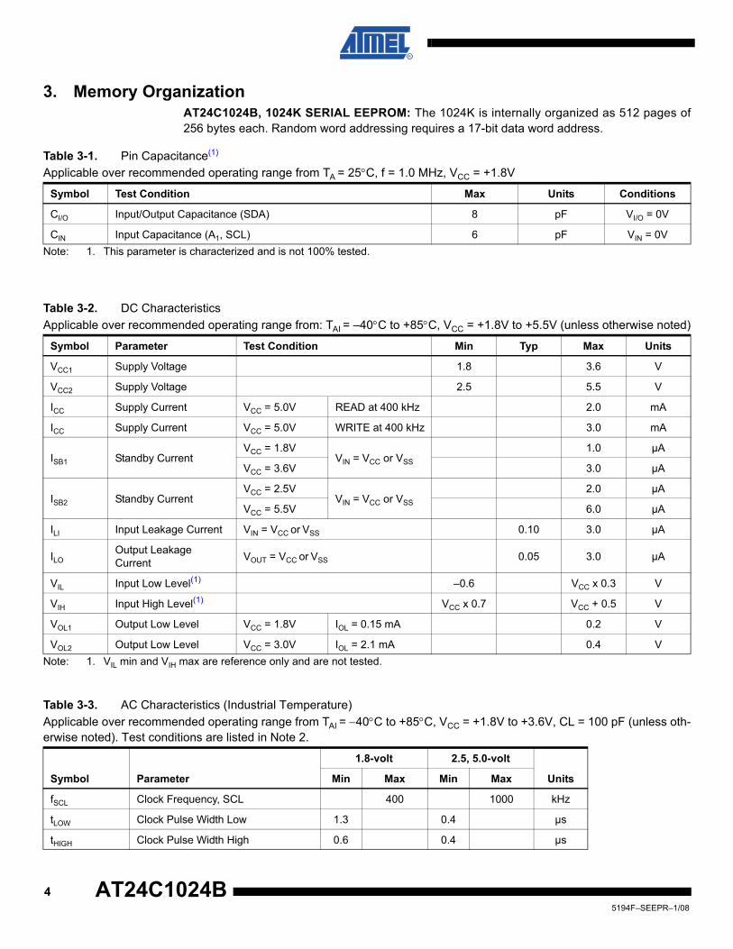
3. Memory OrganizationAT24C1024B, 1024K SERIAL EEPROM: The 1024K is internally organized as 512 pages of256 bytes each. Random word addressing requires a 17-bit data word address.
Note: 1. This parameter is characterized and is not 100% tested.
Note: 1. VIL min and VIH max are reference only and are not tested.
Table 3-1. Pin Capacitance(1)
Applicable over recommended operating range from TA = 25°C, f = 1.0 MHz, VCC = +1.8V
Symbol Test Condition Max Units Conditions
CI/O Input/Output Capacitance (SDA) 8 pF VI/O = 0V
CIN Input Capacitance (A1, SCL) 6 pF VIN = 0V
Table 3-2. DC CharacteristicsApplicable over recommended operating range from: TAI = –40°C to +85°C, VCC = +1.8V to +5.5V (unless otherwise noted)
Symbol Parameter Test Condition Min Typ Max Units
VCC1 Supply Voltage 1.8 3.6 V
VCC2 Supply Voltage 2.5 5.5 V
ICC Supply Current VCC = 5.0V READ at 400 kHz 2.0 mA
ICC Supply Current VCC = 5.0V WRITE at 400 kHz 3.0 mA
ISB1 Standby CurrentVCC = 1.8V
VIN = VCC or VSS
1.0 µA
VCC = 3.6V 3.0 µA
ISB2 Standby CurrentVCC = 2.5V
VIN = VCC or VSS
2.0 µA
VCC = 5.5V 6.0 µA
ILI Input Leakage Current VIN = VCC or VSS 0.10 3.0 µA
ILOOutput Leakage Current VOUT = VCC or VSS 0.05 3.0 µA
VIL Input Low Level(1) –0.6 VCC x 0.3 V
VIH Input High Level(1) VCC x 0.7 VCC + 0.5 V
VOL1 Output Low Level VCC = 1.8V IOL = 0.15 mA 0.2 V
VOL2 Output Low Level VCC = 3.0V IOL = 2.1 mA 0.4 V
Table 3-3. AC Characteristics (Industrial Temperature)Applicable over recommended operating range from TAI = −40°C to +85°C, VCC = +1.8V to +3.6V, CL = 100 pF (unless oth-erwise noted). Test conditions are listed in Note 2.
Symbol Parameter
1.8-volt 2.5, 5.0-volt
UnitsMin Max Min Max
fSCL Clock Frequency, SCL 400 1000 kHz
tLOW Clock Pulse Width Low 1.3 0.4 µs
tHIGH Clock Pulse Width High 0.6 0.4 µs
45194F–SEEPR–1/08
AT24C1024B
AT24C1024B
Notes: 1. This parameter is ensured by characterization only.2. AC measurement conditions:
RL (connects to VCC): 1.3 kΩ (2.5V, 5V), 10 kΩ (1.8V)Input pulse voltages: 0.3 VCC to 0.7 VCCInput rise and fall times: ≤ 50 nsInput and output timing reference voltages: 0.5 VCC
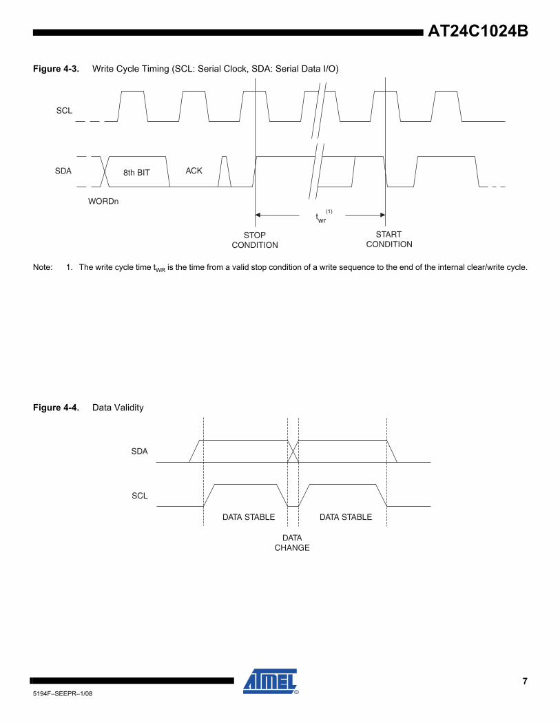
4. Device OperationCLOCK and DATA TRANSITIONS: The SDA pin is normally pulled high with an externaldevice. Data on the SDA pin may change only during SCL low time periods (see Figure 4-4 onpage 7). Data changes during SCL high periods will indicate a start or stop condition as definedbelow.
ti Noise Suppression Time(1) 100 50 ns
tAA Clock Low to Data Out Valid 0.05 0.9 0.05 0.55 µs
tBUFTime the bus must be free before a new transmission can start(1) 1.3 0.5 µs
tHD.STA Start Hold Time 0.6 0.25 µs
tSU.STA Start Set-up Time 0.6 0.25 µs
tHD.DAT Data In Hold Time 0 0 µs
tSU.DAT Data In Set-up Time 100 100 ns
tR Inputs Rise Time(1) 0.3 0.3 µs
tF Inputs Fall Time(1) 300 100 ns
tSU.STO Stop Set-up Time 0.6 0.25 µs
tDH Data Out Hold Time 50 50 ns
tWR Write Cycle Time 5 5 ms
Endurance(1) 25°C, Page Mode, 3.3V 1,000,000 Write Cycles
Table 3-3. AC Characteristics (Industrial Temperature)Applicable over recommended operating range from TAI = −40°C to +85°C, VCC = +1.8V to +3.6V, CL = 100 pF (unless oth-erwise noted). Test conditions are listed in Note 2.
Symbol Parameter
1.8-volt 2.5, 5.0-volt
UnitsMin Max Min Max
55194F–SEEPR–1/08
START CONDITION: A high-to-low transition of SDA with SCL high is a start condition whichmust precede any other command (see Figure 4-5 on page 8).
STOP CONDITION: A low-to-high transition of SDA with SCL high is a stop condition. After aread sequence, the Stop command will place the EEPROM in a standby power mode (see Fig-ure 4-5 on page 8).
ACKNOWLEDGE: All addresses and data words are serially transmitted to and from theEEPROM in 8-bit words. The EEPROM sends a zero during the ninth clock cycle to acknowl-edge that it has received each word.
STANDBY MODE: The AT24C1024B features a low-power standby mode which is enabled: a)upon power-up and b) after the receipt of the stop bit and the completion of any internaloperations.
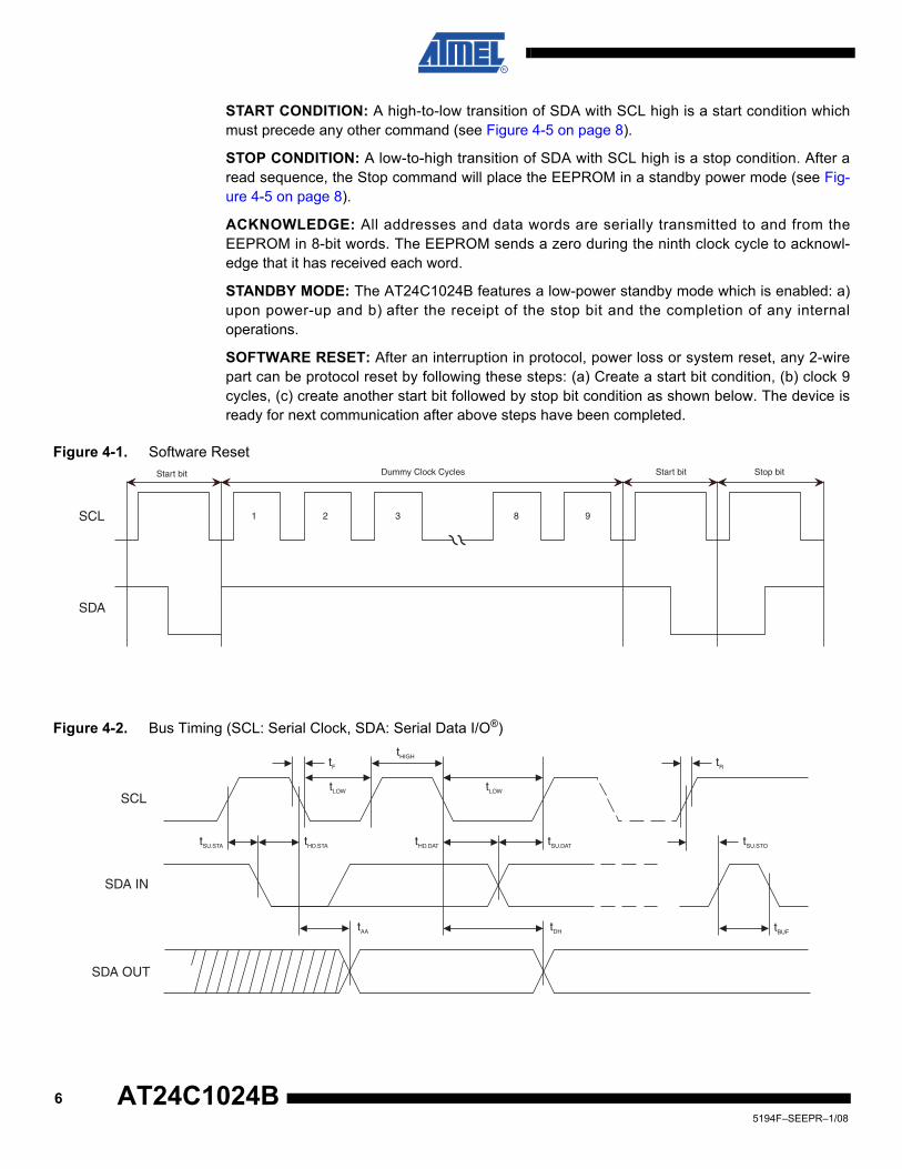
SOFTWARE RESET: After an interruption in protocol, power loss or system reset, any 2-wirepart can be protocol reset by following these steps: (a) Create a start bit condition, (b) clock 9cycles, (c) create another start bit followed by stop bit condition as shown below. The device isready for next communication after above steps have been completed.
Figure 4-1. Software Reset
Figure 4-2. Bus Timing (SCL: Serial Clock, SDA: Serial Data I/O®)
Start bit Stop bitStart bitDummy Clock Cycles
SCL
SDA
1 2 3 8 9
SCL
SDA IN
SDA OUT
tF
tHIGH
tLOW tLOW
tR
tAA tDH tBUF
tSU.STOtSU.DATtHD.DATtHD.STAtSU.STA
65194F–SEEPR–1/08
AT24C1024B
AT24C1024B
Figure 4-3. Write Cycle Timing (SCL: Serial Clock, SDA: Serial Data I/O)
Note: 1. The write cycle time tWR is the time from a valid stop condition of a write sequence to the end of the internal clear/write cycle.
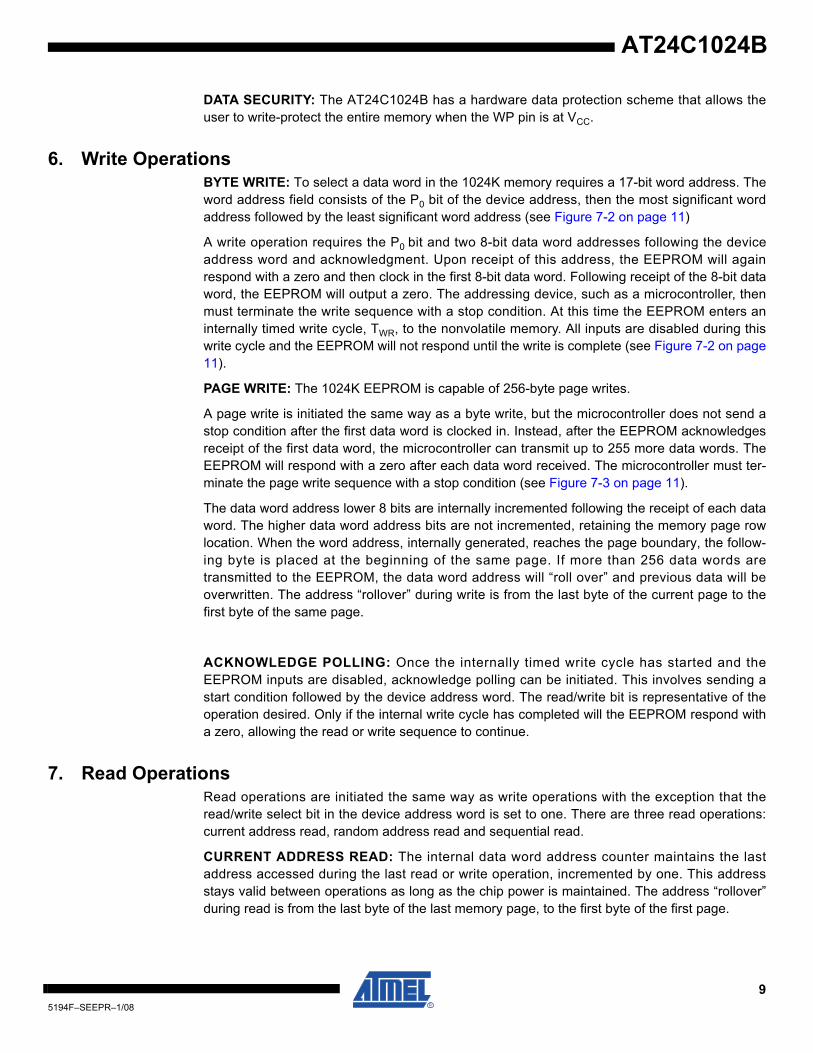
Figure 4-4. Data Validity
twr(1)
STOP CONDITION
START CONDITION
WORDn
ACK8th BIT
SCL
SDA
SDA
SCL
DATA STABLE DATA STABLE
DATACHANGE
75194F–SEEPR–1/08
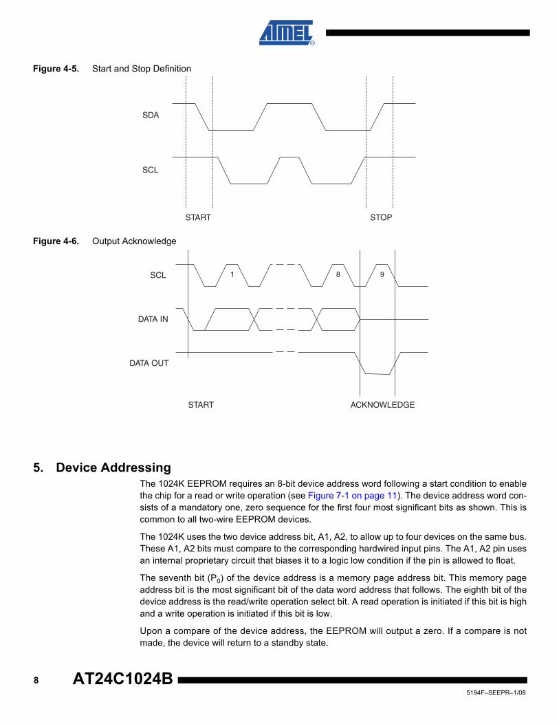
Figure 4-5. Start and Stop Definition
Figure 4-6. Output Acknowledge
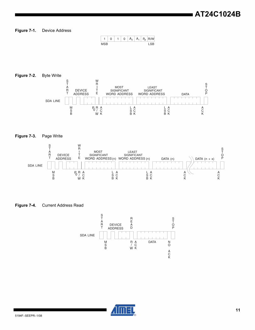
5. Device AddressingThe 1024K EEPROM requires an 8-bit device address word following a start condition to enablethe chip for a read or write operation (see Figure 7-1 on page 11). The device address word con-sists of a mandatory one, zero sequence for the first four most significant bits as shown. This iscommon to all two-wire EEPROM devices.
The 1024K uses the two device address bit, A1, A2, to allow up to four devices on the same bus.These A1, A2 bits must compare to the corresponding hardwired input pins. The A1, A2 pin usesan internal proprietary circuit that biases it to a logic low condition if the pin is allowed to float.
The seventh bit (P0) of the device address is a memory page address bit. This memory pageaddress bit is the most significant bit of the data word address that follows. The eighth bit of thedevice address is the read/write operation select bit. A read operation is initiated if this bit is highand a write operation is initiated if this bit is low.
Upon a compare of the device address, the EEPROM will output a zero. If a compare is notmade, the device will return to a standby state.
SDA
SCL
START STOP
SCL
DATA IN
DATA OUT
START ACKNOWLEDGE
981
85194F–SEEPR–1/08
AT24C1024B
AT24C1024B
DATA SECURITY: The AT24C1024B has a hardware data protection scheme that allows theuser to write-protect the entire memory when the WP pin is at VCC.
6. Write OperationsBYTE WRITE: To select a data word in the 1024K memory requires a 17-bit word address. Theword address field consists of the P0 bit of the device address, then the most significant wordaddress followed by the least significant word address (see Figure 7-2 on page 11)
A write operation requires the P0 bit and two 8-bit data word addresses following the deviceaddress word and acknowledgment. Upon receipt of this address, the EEPROM will againrespond with a zero and then clock in the first 8-bit data word. Following receipt of the 8-bit dataword, the EEPROM will output a zero. The addressing device, such as a microcontroller, thenmust terminate the write sequence with a stop condition. At this time the EEPROM enters aninternally timed write cycle, TWR, to the nonvolatile memory. All inputs are disabled during thiswrite cycle and the EEPROM will not respond until the write is complete (see Figure 7-2 on page11).
PAGE WRITE: The 1024K EEPROM is capable of 256-byte page writes.
A page write is initiated the same way as a byte write, but the microcontroller does not send astop condition after the first data word is clocked in. Instead, after the EEPROM acknowledgesreceipt of the first data word, the microcontroller can transmit up to 255 more data words. TheEEPROM will respond with a zero after each data word received. The microcontroller must ter-minate the page write sequence with a stop condition (see Figure 7-3 on page 11).
The data word address lower 8 bits are internally incremented following the receipt of each dataword. The higher data word address bits are not incremented, retaining the memory page rowlocation. When the word address, internally generated, reaches the page boundary, the follow-ing byte is placed at the beginning of the same page. If more than 256 data words aretransmitted to the EEPROM, the data word address will “roll over” and previous data will beoverwritten. The address “rollover” during write is from the last byte of the current page to thefirst byte of the same page.
ACKNOWLEDGE POLLING: Once the internally timed write cycle has started and theEEPROM inputs are disabled, acknowledge polling can be initiated. This involves sending astart condition followed by the device address word. The read/write bit is representative of theoperation desired. Only if the internal write cycle has completed will the EEPROM respond witha zero, allowing the read or write sequence to continue.
7. Read OperationsRead operations are initiated the same way as write operations with the exception that theread/write select bit in the device address word is set to one. There are three read operations:current address read, random address read and sequential read.
CURRENT ADDRESS READ: The internal data word address counter maintains the lastaddress accessed during the last read or write operation, incremented by one. This addressstays valid between operations as long as the chip power is maintained. The address “rollover”during read is from the last byte of the last memory page, to the first byte of the first page.
95194F–SEEPR–1/08

Once the device address with the read/write select bit set to one is clocked in and acknowledgedby the EEPROM, the current address data word is serially clocked out. The microcontroller doesnot respond with an input zero but does generate a following stop condition (see Figure 7-4 onpage 11).
RANDOM READ: A random read requires a “dummy” byte write sequence to load in the dataword address. Once the device address word and data word address are clocked in andacknowledged by the EEPROM, the microcontroller must generate another start condition. Themicrocontroller now initiates a current address read by sending a device address with theread/write select bit high. The EEPROM acknowledges the device address and serially clocksout the data word. The microcontroller does not respond with a zero but does generate a follow-ing stop condition (see Figure 7-5 on page 12).
SEQUENTIAL READ: Sequential reads are initiated by either a current address read or a ran-dom address read. After the microcontroller receives a data word, it responds with anacknowledge. As long as the EEPROM receives an acknowledge, it will continue to incrementthe data word address and serially clock out sequential data words. When the memory addresslimit is reached, the data word address will “roll over” and the sequential read will continue. Thesequential read operation is terminated when the microcontroller does not respond with a zero,but does generate a following stop condition (see Figure 7-6 on page 12).
105194F–SEEPR–1/08
AT24C1024B
AT24C1024B
Figure 7-1. Device Address
Figure 7-2. Byte Write
Figure 7-3. Page Write
Figure 7-4. Current Address Read
0A2
SIGNIFICANTMOST
SIGNIFICANTLEAST
P0
P0
SIGNIFICANTMOST
SIGNIFICANTLEAST
115194F–SEEPR–1/08
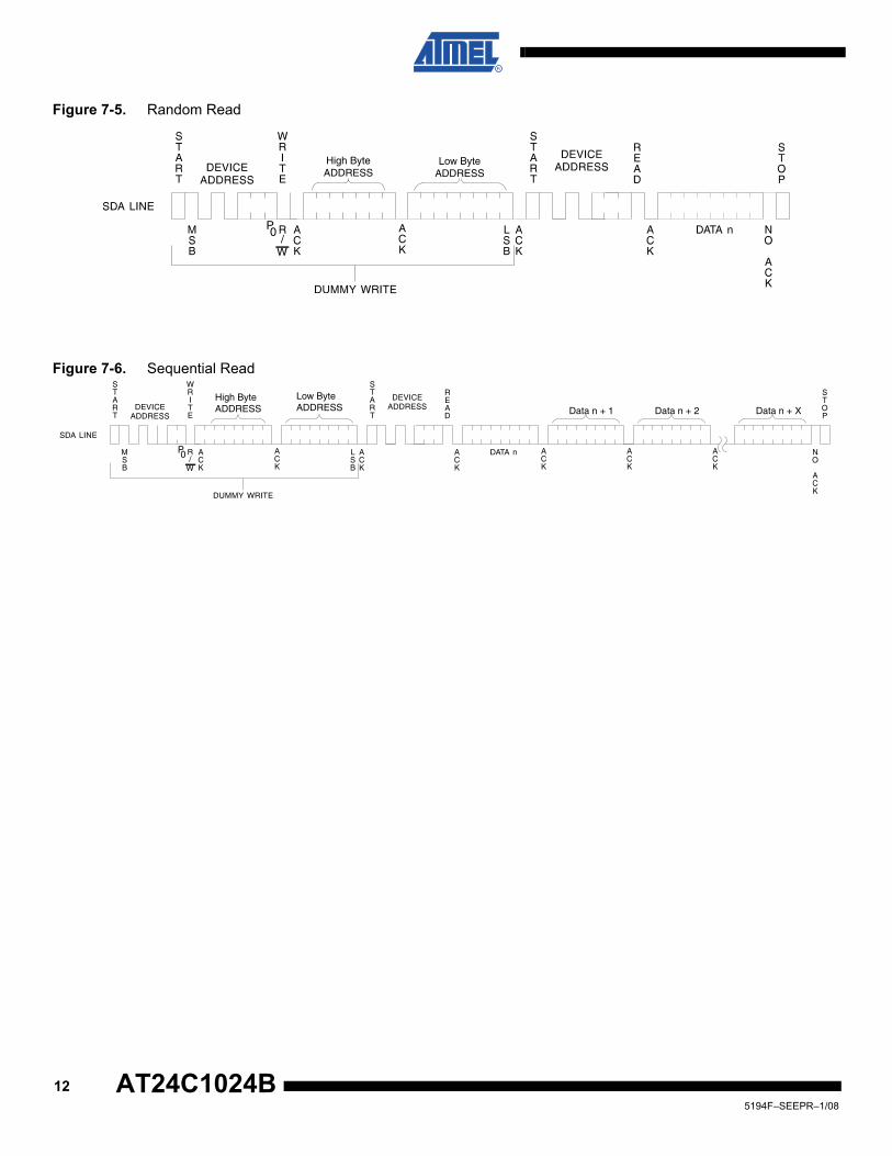
Figure 7-5. Random Read
Figure 7-6. Sequential Read
P 0
High Byte ADDRESS
Low Byte ADDRESS
P 0
High Byte ADDRESS
Low Byte ADDRESS Data n + 1 Data n + 2 Data n + X
125194F–SEEPR–1/08
AT24C1024B
AT24C1024B
Notes: 1. “-B” denotes bulk2. “-T” denotes tape and reel. SOIC = 4K per reel. TSSOP and dBGA2 = 5K per reel. SAP = 3K per reel. EIAJ = 2K per reel.3. Available in tape and reel and wafer form; order as SL788 for inkless wafer form. Bumped die available upon request.
Please contact Serial Interface Marketing.
Ordering InformationOrdering Code Voltage Package Operation RangeAT24C1024B-PU (Bulk form only) 1.8 8P3
Lead-free/Halogen-free/Industrial Temperature
(–40°C to 85°C)
AT24C1024B-PU25 (Bulk form only) 2.5 8P3
AT24C1024BN-SH-B(1) (NiPdAu Lead Finish) 1.8 8S1
AT24C1024BN-SH-T(2) (NiPdAu Lead Finish) 1.8 8S1
AT24C1024BN-SH25-B(1) (NiPdAu Lead Finish) 2.5 8S1
AT24C1024BN-SH25-T(2) (NiPdAu Lead Finish) 2.5 8S1
AT24C1024BW-SH-B(1) (NiPdAu Lead Finish) 1.8 8S2
AT24C1024BW-SH-T(2) (NiPdAu Lead Finish) 1.8 8S2
AT24C1024BW-SH25-B(1) (NiPdAu Lead Finish) 2.5 8S2
AT24C1024BW-SH25-T(2) (NiPdAu Lead Finish) 2.5 8S2
AT24C1024B-TH-B(1) (NiPdAu Lead Finish) 1.8 8A2
AT24C1024B-TH-T(2) (NiPdAu Lead Finish) 1.8 8A2
AT24C1024B-TH25-B(1) (NiPdAu Lead Finish) 2.5 8A2
AT24C1024B-TH25-T(2) (NiPdAu Lead Finish) 2.5 8A2
AT24C1024BY7-YH-T(2) (NiPdAu Lead Finish) 1.8 8Y7
AT24C1024BY7-YH25-T(2) (NiPdAu Lead Finish) 2.5 8Y7
AT24C1024BU4-UU-T(2) 1.8 8U4-1
AT24C1024B-W-11(3) 1.8 Die Sale Industrial Temperature(–40°C to 85°C)
Package Type
8P3 8-lead, 0.300" Wide, Plastic Dual In-line Package (PDIP)
8S1 8-lead, 0.150” Wide, Plastic Gull Wing Small Outline Package (JEDEC SOIC)
8S2 8-lead, 0.200” Wide Plastic Gull Wing Small Outline Package (EIAJ SOIC)
8A2 8-lead, 4.4 mm Body, Plastic Thin Shrink Small Outline Package (TSSOP)
8Y7 8-lead, 6.00 mm x 4.90 mm Body, Ultra Thin, Dual Footprint, Non-leaded, Small Array Package (SAP)
8U4-1 8-ball, die Ball Grid Array Package (dBGA2)
Options
–1.8 Low-voltage (1.8V to 3.6V)
–2.5 Low-voltage (2.5V to 5.5V)
135194F–SEEPR–1/08
8. Part marking scheme
8.1 8-SOIC(1.8V)
8.2 8-SOIC(2.5V)
TOP MARK Seal Year Y = SEAL YEAR WW = SEAL WEEK | Seal Week 6: 2006 0: 2010 02 = Week 2
| | | 7: 2007 1: 2011 04 = Week 4 |---|---|---|---|---|---|---|---| 8: 2008 2: 2012 :: : :::: : A T M L H Y W W 9: 2009 3: 2013 :: : :::: ::
|---|---|---|---|---|---|---|---| 50 = Week 50
2 G B 1 52 = Week 52
|---|---|---|---|---|---|---|---| * Lot Number Lot Number to Use ALL Characters in Marking |---|---|---|---|---|---|---|---| | BOTTOM MARK Pin 1 Indicator (Dot) No Bottom Mark
TOP MARK Seal Year Y = SEAL YEAR WW = SEAL WEEK | Seal Week 6: 2006 0: 2010 02 = Week 2
| | | 7: 2007 1: 2011 04 = Week 4 |---|---|---|---|---|---|---|---| 8: 2008 2: 2012 :: : :::: : A T M L H Y W W 9: 2009 3: 2013 :: : :::: ::
|---|---|---|---|---|---|---|---| 50 = Week 50
2 G B 2 52 = Week 52
|---|---|---|---|---|---|---|---| * Lot Number Lot Number to Use ALL Characters in Marking |---|---|---|---|---|---|---|---| | BOTTOM MARK Pin 1 Indicator (Dot) No Bottom Mark
145194F–SEEPR–1/08
AT24C1024B
AT24C1024B
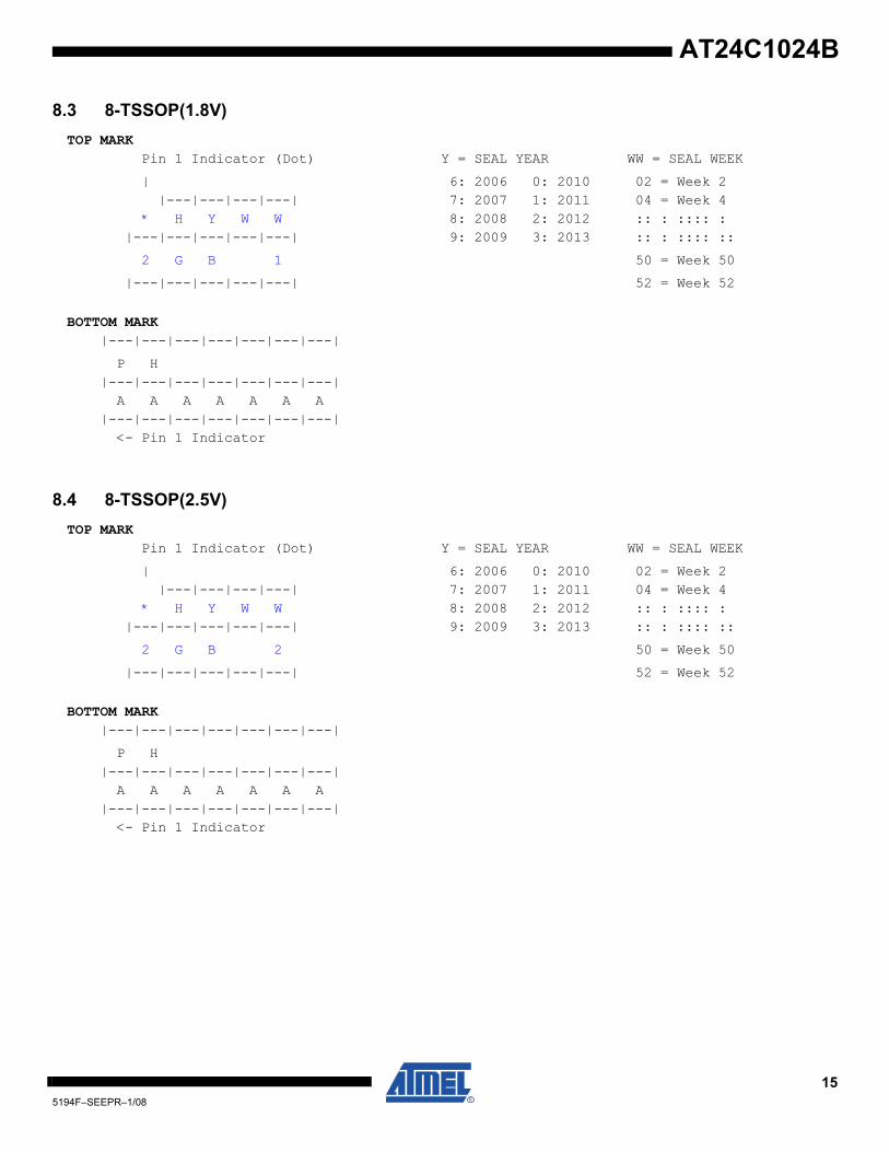
8.3 8-TSSOP(1.8V)
8.4 8-TSSOP(2.5V)
TOP MARK Pin 1 Indicator (Dot) Y = SEAL YEAR WW = SEAL WEEK
| 6: 2006 0: 2010 02 = Week 2 |---|---|---|---| 7: 2007 1: 2011 04 = Week 4 * H Y W W 8: 2008 2: 2012 :: : :::: : |---|---|---|---|---| 9: 2009 3: 2013 :: : :::: ::
2 G B 1 50 = Week 50
|---|---|---|---|---| 52 = Week 52
BOTTOM MARK |---|---|---|---|---|---|---|
P H |---|---|---|---|---|---|---| A A A A A A A |---|---|---|---|---|---|---| <- Pin 1 Indicator
TOP MARK Pin 1 Indicator (Dot) Y = SEAL YEAR WW = SEAL WEEK
| 6: 2006 0: 2010 02 = Week 2 |---|---|---|---| 7: 2007 1: 2011 04 = Week 4 * H Y W W 8: 2008 2: 2012 :: : :::: : |---|---|---|---|---| 9: 2009 3: 2013 :: : :::: ::
2 G B 2 50 = Week 50
|---|---|---|---|---| 52 = Week 52
BOTTOM MARK |---|---|---|---|---|---|---|
P H |---|---|---|---|---|---|---| A A A A A A A |---|---|---|---|---|---|---| <- Pin 1 Indicator
155194F–SEEPR–1/08
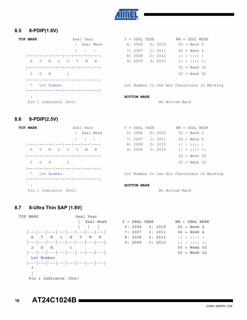
8.5 8-PDIP(1.8V)
8.6 8-PDIP(2.5V)
8.7 8-Ultra Thin SAP (1.8V)
TOP MARK Seal Year Y = SEAL YEAR WW = SEAL WEEK | Seal Week 6: 2006 0: 2010 02 = Week 2
| | | 7: 2007 1: 2011 04 = Week 4 |---|---|---|---|---|---|---|---| 8: 2008 2: 2012 :: : :::: : A T M L U Y W W 9: 2009 3: 2013 :: : :::: ::
|---|---|---|---|---|---|---|---| 50 = Week 50
2 G B 1 52 = Week 52
|---|---|---|---|---|---|---|---| * Lot Number Lot Number to Use ALL Characters in Marking |---|---|---|---|---|---|---|---|
| BOTTOM MARK Pin 1 Indicator (Dot) No Bottom Mark
TOP MARK Seal Year Y = SEAL YEAR WW = SEAL WEEK | Seal Week 6: 2006 0: 2010 02 = Week 2
| | | 7: 2007 1: 2011 04 = Week 4 |---|---|---|---|---|---|---|---| 8: 2008 2: 2012 :: : :::: : A T M L U Y W W 9: 2009 3: 2013 :: : :::: ::
|---|---|---|---|---|---|---|---| 50 = Week 50
2 G B 2 52 = Week 52
|---|---|---|---|---|---|---|---| * Lot Number Lot Number to Use ALL Characters in Marking |---|---|---|---|---|---|---|---|
| BOTTOM MARK Pin 1 Indicator (Dot) No Bottom Mark
TOP MARK Seal Year | Seal Week Y = SEAL YEAR WW = SEAL WEEK | | | 6: 2006 0: 2010 02 = Week 2
|---|---|---|---|---|---|---|---| 7: 2007 1: 2011 04 = Week 4 A T M L H Y W W 8: 2008 2: 2012 :: : :::: : |---|---|---|---|---|---|---|---| 9: 2009 3: 2013 :: : :::: :: 2 G B 1 50 = Week 50 |---|---|---|---|---|---|---|---| 52 = Week 52 Lot Number |---|---|---|---|---|---|---|---| * | Pin 1 Indicator (Dot)
165194F–SEEPR–1/08
AT24C1024B
AT24C1024B
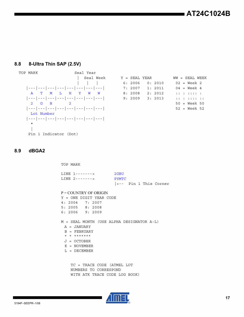
8.8 8-Ultra Thin SAP (2.5V)
8.9 dBGA2
TOP MARK Seal Year | Seal Week Y = SEAL YEAR WW = SEAL WEEK | | | 6: 2006 0: 2010 02 = Week 2
|---|---|---|---|---|---|---|---| 7: 2007 1: 2011 04 = Week 4 A T M L H Y W W 8: 2008 2: 2012 :: : :::: : |---|---|---|---|---|---|---|---| 9: 2009 3: 2013 :: : :::: :: 2 G B 2 50 = Week 50 |---|---|---|---|---|---|---|---| 52 = Week 52 Lot Number |---|---|---|---|---|---|---|---| * | Pin 1 Indicator (Dot)
TOP MARK
LINE 1-------> 2GBULINE 2-------> PYMTC |<-- Pin 1 This Corner
P = COUNTRY OF ORIGINY = ONE DIGIT YEAR CODE4: 2004 7: 20075: 2005 8: 20086: 2006 9: 2009
M = SEAL MONTH (USE ALPHA DESIGNATOR A-L) A = JANUARY B = FEBRUARY " " """"""" J = OCTOBER K = NOVEMBER L = DECEMBER
TC = TRACE CODE (ATMEL LOT NUMBERS TO CORRESPOND WITH ATK TRACE CODE LOG BOOK)
175194F–SEEPR–1/08
9. Packaging Information
8P3 – PDIP
2325 Orchard ParkwaySan Jose, CA 95131
TITLE DRAWING NO.
R
REV. 8P3, 8-lead, 0.300" Wide Body, Plastic Dual In-line Package (PDIP)
01/09/02
8P3 B
Notes: 1. This drawing is for general information only; refer to JEDEC Drawing MS-001, Variation BA, for additional information. 2. Dimensions A and L are measured with the package seated in JEDEC seating plane Gauge GS-3. 3. D, D1 and E1 dimensions do not include mold Flash or protrusions. Mold Flash or protrusions shall not exceed 0.010 inch. 4. E and eA measured with the leads constrained to be perpendicular to datum. 5. Pointed or rounded lead tips are preferred to ease insertion. 6. b2 and b3 maximum dimensions do not include Dambar protrusions. Dambar protrusions shall not exceed 0.010 (0.25 mm).
COMMON DIMENSIONS(Unit of Measure = inches)
SYMBOL MIN NOM MAX NOTE
D
D1
E
E1
e
Lb2
b
A2 A
1
N
eAc
b34 PLCS
A – – 0.210 2
A2 0.115 0.130 0.195
b 0.014 0.018 0.022 5
b2 0.045 0.060 0.070 6
b3 0.030 0.039 0.045 6
c 0.008 0.010 0.014
D 0.355 0.365 0.400 3
D1 0.005 – – 3
E 0.300 0.310 0.325 4
E1 0.240 0.250 0.280 3
e 0.100 BSC
eA 0.300 BSC 4
L 0.115 0.130 0.150 2
Top View
Side View
End View
185194F–SEEPR–1/08
AT24C1024B
AT24C1024B
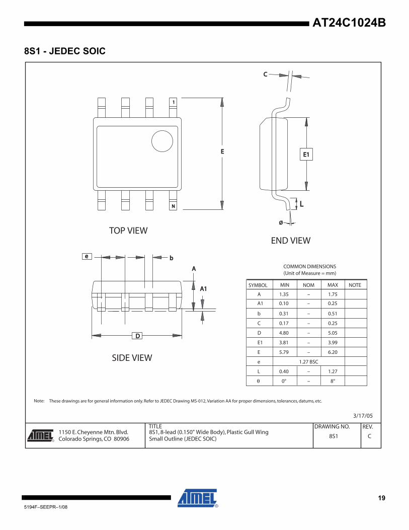
8S1 - JEDEC SOIC
1150 E. Cheyenne Mtn. Blvd.Colorado Springs, CO 80906
TITLE DRAWING NO.
R
REV.
Note:
3/17/05
8S1, 8-lead (0.150" Wide Body), Plastic Gull Wing Small Outline (JEDEC SOIC) 8S1 C
COMMON DIMENSIONS(Unit of Measure = mm)
SYMBOL MIN NOM MAX NOTE
A1 0.10 – 0.25
These drawings are for general information only. Refer to JEDEC Drawing MS-012, Variation AA for proper dimensions, tolerances, datums, etc.
A 1.35 – 1.75
b 0.31 – 0.51
C 0.17 – 0.25
D 4.80 – 5.05
E1 3.81 – 3.99
E 5.79 – 6.20
e 1.27 BSC
L 0.40 – 1.27
θ 0° – 8°
ØØ
EE
11
NN
TOP VIEW
CC
E1E1
END VIEW
AA
bb
LL
A1A1
ee
DD
SIDE VIEW
195194F–SEEPR–1/08
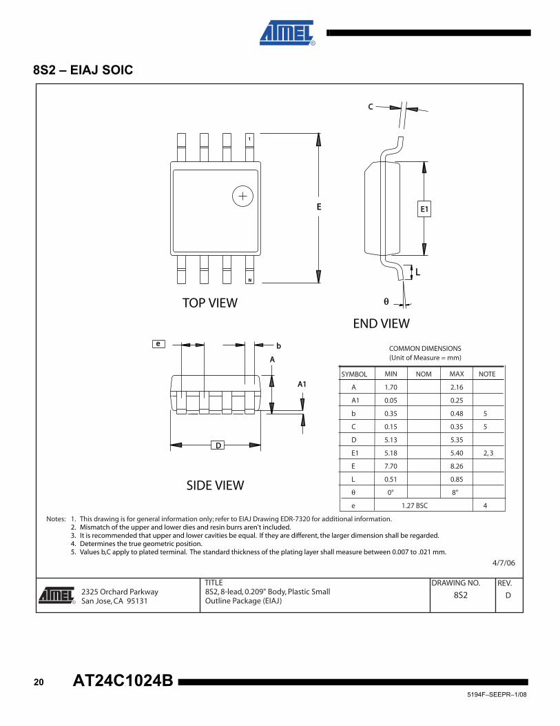
8S2 – EIAJ SOIC
2325 Orchard ParkwaySan Jose, CA 95131
TITLE DRAWING NO.
R
REV. 8S2, 8-lead, 0.209" Body, Plastic Small Outline Package (EIAJ)
4/7/06
8S2 D
COMMON DIMENSIONS(Unit of Measure = mm)
SYMBOL MIN NOM MAX NOTE
Notes: 1. This drawing is for general information only; refer to EIAJ Drawing EDR-7320 for additional information. 2. Mismatch of the upper and lower dies and resin burrs aren't included. 3. It is recommended that upper and lower cavities be equal. If they are different, the larger dimension shall be regarded. 4. Determines the true geometric position. 5. Values b,C apply to plated terminal. The standard thickness of the plating layer shall measure between 0.007 to .021 mm.
A 1.70 2.16
A1 0.05 0.25
b 0.35 0.48 5
C 0.15 0.35 5
D 5.13 5.35
E1 5.18 5.40 2, 3
E 7.70 8.26
L 0.51 0.85
θ 0° 8°
e 1.27 BSC 4
θθ
11
NN
EE
TOP VIEW
CC
E1E1
END VIEW
AA
bb
LL
A1A1
ee
DD
SIDE VIEW
205194F–SEEPR–1/08
AT24C1024B
AT24C1024B
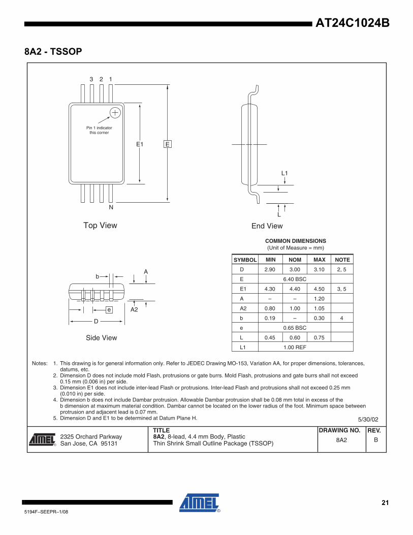
8A2 - TSSOP
2325 Orchard ParkwaySan Jose, CA 95131
TITLE DRAWING NO.
R
REV.
5/30/02
COMMON DIMENSIONS(Unit of Measure = mm)
SYMBOL MIN NOM MAX NOTE
D 2.90 3.00 3.10 2, 5
E 6.40 BSC
E1 4.30 4.40 4.50 3, 5
A – – 1.20
A2 0.80 1.00 1.05
b 0.19 – 0.30 4
e 0.65 BSC
L 0.45 0.60 0.75
L1 1.00 REF
8A2, 8-lead, 4.4 mm Body, Plastic Thin Shrink Small Outline Package (TSSOP)
Notes: 1. This drawing is for general information only. Refer to JEDEC Drawing MO-153, Variation AA, for proper dimensions, tolerances, datums, etc.
2. Dimension D does not include mold Flash, protrusions or gate burrs. Mold Flash, protrusions and gate burrs shall not exceed 0.15 mm (0.006 in) per side.
3. Dimension E1 does not include inter-lead Flash or protrusions. Inter-lead Flash and protrusions shall not exceed 0.25 mm (0.010 in) per side.
4. Dimension b does not include Dambar protrusion. Allowable Dambar protrusion shall be 0.08 mm total in excess of the b dimension at maximum material condition. Dambar cannot be located on the lower radius of the foot. Minimum space between protrusion and adjacent lead is 0.07 mm.
5. Dimension D and E1 to be determined at Datum Plane H.
8A2 B
Side View
End ViewTop View
A2
A
L
L1
D
123
E1
N
b
Pin 1 indicatorthis corner
E
e
215194F–SEEPR–1/08
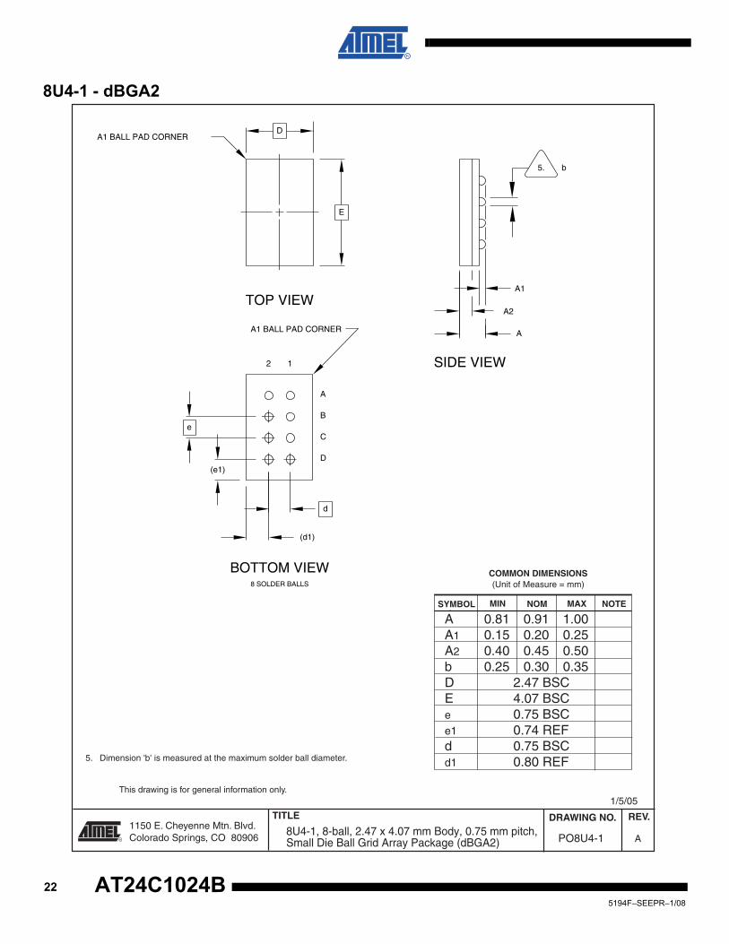
8U4-1 - dBGA2
1150 E. Cheyenne Mtn. Blvd.Colorado Springs, CO 80906
TITLE DRAWING NO.
R
REV.
PO8U4-1 A
1/5/05
COMMON DIMENSIONS(Unit of Measure = mm)
SYMBOL MIN NOM MAX NOTE
8U4-1, 8-ball, 2.47 x 4.07 mm Body, 0.75 mm pitch, Small Die Ball Grid Array Package (dBGA2)
A 0.81 0.91 1.00A1 0.15 0.20 0.25A2 0.40 0.45 0.50b 0.25 0.30 0.35D 2.47 BSCE 4.07 BSCe 0.75 BSCe1 0.74 REFd 0.75 BSCd1 0.80 REF
5. Dimension 'b' is measured at the maximum solder ball diameter.
This drawing is for general information only.
d
A
SIDE VIEW
TOP VIEW
8 SOLDER BALLS
BOTTOM VIEW
1
A
B
C
D
2
(e1)
e
A1 BALL PAD CORNER
(d1)
5. b
A1
A2
DA1 BALL PAD CORNER
E
225194F–SEEPR–1/08
AT24C1024B
AT24C1024B
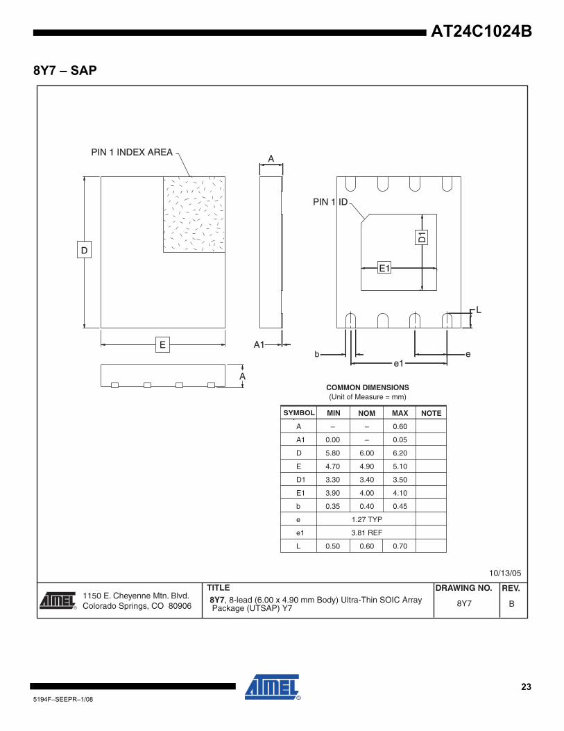
8Y7 – SAP
1150 E. Cheyenne Mtn. Blvd.Colorado Springs, CO 80906
TITLE DRAWING NO.
R
REV. 8Y7, 8-lead (6.00 x 4.90 mm Body) Ultra-Thin SOIC Array Package (UTSAP) Y7 B8Y7
10/13/05
COMMON DIMENSIONS(Unit of Measure = mm)
SYMBOL MIN NOM MAX NOTE
A – – 0.60
A1 0.00 – 0.05
D 5.80 6.00 6.20
E 4.70 4.90 5.10
D1 3.30 3.40 3.50
E1 3.90 4.00 4.10
b 0.35 0.40 0.45
e 1.27 TYP
e1 3.81 REF
L 0.50 0.60 0.70
D1
PIN 1 ID
E1
L
be1
e
PIN 1 INDEX AREA
A
E
D
A1
A
235194F–SEEPR–1/08
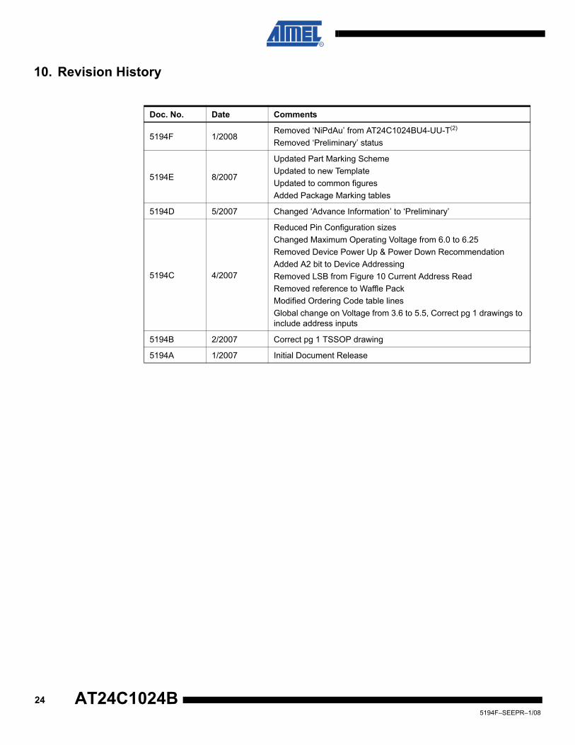
10. Revision History
Doc. No. Date Comments
5194F 1/2008Removed ‘NiPdAu’ from AT24C1024BU4-UU-T(2)
Removed ‘Preliminary’ status
5194E 8/2007
Updated Part Marking SchemeUpdated to new TemplateUpdated to common figuresAdded Package Marking tables
5194D 5/2007 Changed ‘Advance Information’ to ‘Preliminary’
5194C 4/2007
Reduced Pin Configuration sizesChanged Maximum Operating Voltage from 6.0 to 6.25Removed Device Power Up & Power Down RecommendationAdded A2 bit to Device AddressingRemoved LSB from Figure 10 Current Address ReadRemoved reference to Waffle PackModified Ordering Code table linesGlobal change on Voltage from 3.6 to 5.5, Correct pg 1 drawings to include address inputs
5194B 2/2007 Correct pg 1 TSSOP drawing
5194A 1/2007 Initial Document Release
245194F–SEEPR–1/08
AT24C1024B
5194F–SEEPR–1/08
Headquarters International
Atmel Corporation2325 Orchard ParkwaySan Jose, CA 95131USATel: 1(408) 441-0311Fax: 1(408) 487-2600
Atmel AsiaRoom 1219Chinachem Golden Plaza77 Mody Road TsimshatsuiEast KowloonHong KongTel: (852) 2721-9778Fax: (852) 2722-1369
Atmel EuropeLe Krebs8, Rue Jean-Pierre TimbaudBP 30978054 Saint-Quentin-en-Yvelines CedexFranceTel: (33) 1-30-60-70-00 Fax: (33) 1-30-60-71-11
Atmel Japan9F, Tonetsu Shinkawa Bldg.1-24-8 ShinkawaChuo-ku, Tokyo 104-0033JapanTel: (81) 3-3523-3551Fax: (81) 3-3523-7581
Product Contact
Web Sitewww.atmel.com
Technical [email protected]
Sales Contactwww.atmel.com/contacts
Literature Requestswww.atmel.com/literature
Disclaimer: The information in this document is provided in connection with Atmel products. No license, express or implied, by estoppel or otherwise, to anyintellectual property right is granted by this document or in connection with the sale of Atmel products. EXCEPT AS SET FORTH IN ATMEL’S TERMS AND CONDI-TIONS OF SALE LOCATED ON ATMEL’S WEB SITE, ATMEL ASSUMES NO LIABILITY WHATSOEVER AND DISCLAIMS ANY EXPRESS, IMPLIED OR STATUTORYWARRANTY RELATING TO ITS PRODUCTS INCLUDING, BUT NOT LIMITED TO, THE IMPLIED WARRANTY OF MERCHANTABILITY, FITNESS FOR A PARTICULARPURPOSE, OR NON-INFRINGEMENT. IN NO EVENT SHALL ATMEL BE LIABLE FOR ANY DIRECT, INDIRECT, CONSEQUENTIAL, PUNITIVE, SPECIAL OR INCIDEN-TAL DAMAGES (INCLUDING, WITHOUT LIMITATION, DAMAGES FOR LOSS OF PROFITS, BUSINESS INTERRUPTION, OR LOSS OF INFORMATION) ARISING OUTOF THE USE OR INABILITY TO USE THIS DOCUMENT, EVEN IF ATMEL HAS BEEN ADVISED OF THE POSSIBILITY OF SUCH DAMAGES. Atmel makes norepresentations or warranties with respect to the accuracy or completeness of the contents of this document and reserves the right to make changes to specificationsand product descriptions at any time without notice. Atmel does not make any commitment to update the information contained herein. Unless specifically providedotherwise, Atmel products are not suitable for, and shall not be used in, automotive applications. Atmel’s products are not intended, authorized, or warranted for useas components in applications intended to support or sustain life.
©2008 Atmel Corporation. All rights reserved. Atmel®, logo and combinations thereof, are registered trademarks or trademarks of Atmel Cor-poration or its subsidiaries. Other terms and product names may be trademarks of others.