Embed Size (px)
Citation preview
Raman Scattering Study of Lattice Vibrations in the Type-II Superlattice InAs=InAs1−xSbx
Henan Liu and Yong Zhang*
Optical Science and Engineering Graduate Program and Department of Electrical andComputer Engineering, University of North Carolina at Charlotte, Charlotte 28223, North Carolina, USA
Elizabeth H. Steenbergen, Shi Liu, Zhiyuan Lin, and Yong-Hang ZhangCenter for Photonics Innovation and School of Electrical, Computer and Energy Engineering,
Arizona State University, Tempe 85287, Arizona, USA
Jeomoh Kim, Mi-Hee Ji, Theeradetch Detchprohm, and Russell D. DupuisCenter for Compound Semiconductors and School of Electrical and Computer Engineering,
Georgia Institute of Technology, Atlanta 30332, Georgia, USA
Jin K. Kim, Samuel D. Hawkins, and John F. KlemSandia National Laboratories, Albuquerque 87185, New Mexico, USA
(Received 7 November 2016; revised manuscript received 9 August 2017; published 26 September 2017)
The InAs=InAs1−xSbx superlattice system distinctly differs from two well-studied superlattice systemsGaAs=AlAs and InAs=GaSb in terms of electronic band alignment, common elements at the interface, andphonon spectrum overlapping of the constituents. This fact leads to the unique electronic and vibrationalproperties of the InAs=InAs1−xSbx system when compared to the other two systems. In this work, we reporta polarized Raman study of the vibrational properties of the InAs=InAs1−xSbx superlattices (SLs) as well asselected InAs1−xSbx alloys, all grown on GaSb substrates by either MBE or metalorganic chemical vapordeposition (MOCVD) from both the growth surface and cleaved edge. In the SL, from the (001)backscattering geometry, an InAs-like longitudinal optical (LO) mode is observed as the primary feature,and its intensity is found to increase with increasing Sb composition. From the (110) cleaved-edgebackscattering geometry, an InAs-like transverse optical (TO) mode is observed as the main feature in twocross-polarization configurations, but an additional InAs-like “forbidden” LO mode is observed in twoparallel-polarization configurations. The InAs1−xSbx alloys lattice matched to the substrate (xSb ∼ 0.09)grown by MBE are also found to exhibit the forbidden LO mode, implying the existence of someunexpected [001] modulation. However, the strained samples (xSb ∼ 0.35) grown by MOCVD are found tobehave like a disordered alloy. The primary conclusions are (1) the InAs-like LO or TO mode can be eithera confined or quasiconfined mode in the InAs layers of the SL or extended mode of the whole structuredepending on the Sb composition. (2) InAs=InAs1−xSbx and InAs=GaSb SLs exhibit significantly differentbehaviors in the cleaved-edge geometry but qualitatively similar in the (001) geometry. (3) The appearanceof the forbidden LO-like mode is a universal signature for SLs and bulk systems resulting from the mixingof phonon modes due to structural modulation or symmetry reduction.
DOI: 10.1103/PhysRevApplied.8.034028
I. INTRODUCTION
Recently, InAs=InAs1−xSbx type-II superlattices(T2SLs) have received considerable attention as a newIII-V–based infrared (IR) detection material [1,2], analternative to the much more extensively studiedInAs=GaSb T2SLs [3–6] that can complement the widelyused bulk (Hg,Cd)Te alloys in mid- and long-wavelengthinfrared detection [7–10]. Improved minority-carrier life-times and dark currents compared to InAs=GaSb SLs havebeen reported for the InAs=InAs1−xSbx SLs and their
devices [11,12], which are generally believed to be relatedto the absence of Ga in this system [13,14]. Therefore, thisGa-free system is becoming a research area in the fields ofIR detection and basic material physics. In addition to theprimary current interest in IR detection, the T2SLs offer theflexibility that type-I SLs, such as GaAs=AlAs SLs, do nothave; that is, for the T2SLs, the electronic and thermalconductivity along the SL stacking direction can be tailoredseparately. This feature of the IR T2SL is highly desirablefor thermoelectric related applications [15]. Additionally, iflateral contacts can be made separately from the twoconstituent layers to facilitate efficient carrier separation[16], IR T2SLs will be ideally suited for thermophotovol-taic devices [17].
*Corresponding [email protected]
PHYSICAL REVIEW APPLIED 8, 034028 (2017)
2331-7019=17=8(3)=034028(13) 034028-1 © 2017 American Physical Society
In contrast to the considerable recent experimentalefforts towards understanding the optical and electricalproperties of InAs=InAs1−xSbx SLs [1,11,18–22], therehave not been many experimental or theoretical studiesconducted on their vibrational properties or Raman spec-troscopy, except for some early work on the InAs1−xSbxalloys [23,24]. This situation motivates us to conduct aRaman study of the InAs=InAs1−xSbx SLs, aiming to revealand understand their vibrational properties and comparewith two well-studied but distinctly different systems,GaAs=AlAs and InAs=GaSb SLs. This effort will fillthe knowledge gap of our understanding of the Ramanspectroscopy of semiconductor SLs because theInAs=InAs1−xSbx system represents one of the three uniquecategories of SLs. This study lays the foundation for futureefforts, such as exploring the mechanism of electron-phonon-coupling processes, using the results in materialcharacterization, and providing guidance for device appli-cations. Furthermore, this study provides the opportunity touncover a fundamental and universal effect of structuralmodulation on longitudinal optical (LO) phonons in SLsand other modulated systems.The InAs=InAs1−xSbx system is unique when comparing
its vibrational properties to those of the two better-known SLsystems, GaAs=AlAs [25,26] and InAs=GaSb [27]. TheGaAs=AlAs system has type-I or straddling electronic bandalignment, and the optical phonon spectra of the twoconstituents do not overlap (resembling the so-called bro-ken-gap type-II electronic band alignment but for thepropagation band) [25]. InAs=GaSb has the broken-gaptype-II electronic band alignment, and the optical phononspectra of the two constituents overlap with each other butwith one enclosing the other (resembling the type-I electronicband alignment) [28], whereas the InAs=InAs1−xSbx systemhas staggered type-II electronic band alignment as well asstaggered overlapping optical phonon spectra. Furthermore,InAs=GaSb is special, being a no-common-element system,whereas InAs=InAs1−xSbx is a common-cation system.Consequently, the symmetry reduction from D2d in theGaAs=AlAs toC2v in the InAs=GaSb system does not occurin the InAs=InAs1−xSbx system. Therefore, it is of greatinterest to investigate InAs=InAs1−xSbx SLs, which will bebeneficial for understanding the SLphysics for this particularmaterial system and the field in general.One of the important SL effects related to symmetry
reduction has been that the forbidden LO Raman mode inthe (110) backscattering geometry in bulk becomesallowed, which was first observed in GaAs=AlAs SLs[29,30] and explained as arising from a standing wave inthe SL stacking direction z with an effective large wavevector qz [31]. Recently, the effect was observed inInAs=GaSb by some of us and speculated as due to thetransverse mode of the phonon polariton [27]. The sameeffect was also observed in yet another system, a sponta-neously ordered (Ga,In)P alloy—a monolayer superlattice
along the [1̄11] direction [32]. There were two possiblemechanisms given: the q-dependent Fröhlich interactionand the Fröhlich interaction due to the electrical fieldinduced by surface charges, in connection with the similareffect reported for a bulk material (GaAs) with doping [33].We now add two cases, InAs=InAs1−xSbx SLs andInAs1−xSbx alloys, for this is fundamentally a symmetry-breaking-related phenomenon, which allows us to associatethis phenomenon to a universal mechanism: modulation-induced mixing of vibration modes.In this work, we perform polarized micro-Raman mea-
surements on both a (001) growth plane and (110) cleavededge on two sets of InAs=InAs1−xSbx SL samples grown onGaSb substrates, one by molecular-beam epitaxy (MBE) andthe other by metalorganic chemical vapor deposition(MOCVD), togetherwith selected InAs1−xSbx alloy samples,bulk InAs and InSb samples, and alloy and SL samples withGa doping. The reasons to include a large set of samples are asfollows: InAs1−xSbx alloys are known to potentially exhibitboth spontaneous vertical and lateral composition modula-tions, depending on thegrowthmethod and condition [34,35].All the recent studies implicitly assumed the InAs1−xSbxalloy layers in the SLs were disordered, even though sampleswere grown with different techniques. It is also well knownthat both lateral andvertical compositionmodulations in III-Valloys can have major effects in Raman scattering [32,36].Our goal is to obtain the intrinsic properties of the SLassuming the alloy layer being disordered and alert thepotential complications, if any, caused by any unintendedstructural modulation. Therefore, bulk alloys and SLs grownbydifferent techniques are included.Furthermore,we show inour recent study of InAs=GaSb SLs that the relative Ramancross section of the bulk constituents can offer a very helpfulhint to the origin of a Raman mode of the SL [27]. Thus, thebulk binaries are also measured under the same condition.Direct comparison of these samples is found to be importantto understand the intrinsic vibrational properties of the SLsand reveal the subtle differences between the SL structuresgrown by the two growth techniques. Our primary findingsinclude (1) an InAs (quasi-) confined LO mode when xSb isrelatively low and its evolution into an extended SL modewhen xSb increases observed from the front surface meas-urement; (2) an InAs (quasi-) confined transverse optical (TO)mode as well as a “forbidden” LO-like TO mode observedfrom the cleaved-edge measurement; (3) qualitativelydifferent Raman spectra between InAs=InAs1−xSbx andInAs=GaSb when measured from the (110) plane butqualitatively similar behaviors from the (001) plane;(4) the appearance of the LO-like mode in the forbiddengeometry as a common feature in SLs and even bulk alloyswhen the translational symmetry is broken.
II. EXPERIMENT
All Raman measurements are conducted at room temper-ature using a Horiba HR800 confocal Raman microscope
HENAN LIU et al. PHYS. REV. APPLIED 8, 034028 (2017)
034028-2
equipped with a charge-coupled device. The Raman signalsare collected by a 100× Olympus objective lens withnumerical aperture NA ¼ 0.9. The spectrometer is cali-brated to yield the Si Raman peak at 520.7 cm−1. By usinga 532-nm laser, we have a spectral dispersion of0.44 cm−1=pixel and a spatial resolution of approximately0.36 μm. To avoid sample heating, a sufficiently low laserpower (approximately 0.22 mW) is used [27]. Typically, aredshift of approximately 1.5 cm−1 is found for thesesamples when a factor of 10-times-higher laser power isused. Also, two additional Raman modes at approximately131 cm−1 and approximately 151 cm−1 often appear at thehigher power. We do not intend to discuss the details of thehigher-power results, but we wish to point out that thesefeatures reported in the previous study of InAs1−xSbx alloys[24] are actually from local heating-induced formation ofSb elemental crystal [37].All samples are grown on (001) GaSb substrates
either by MBE or MOCVD with their structural infor-mation listed in Table I. The samples are labeled with “S”for superlattice samples and “A” for alloy samples.Because the bulk lattice constant sizes are in the orderof aInAsð6.0584 ÅÞ < aGaSbð6.0959 ÅÞ < aInSbð6.4794 ÅÞ,InAs1−xSbx is lattice matched to the GaSb substrate atxc ¼ 0.089. The SL structure overall is targeted to be latticematched to the substrate, which means that the InAs layerwill be under in-plane tensile strain and the InAs1−xSbx layerunder in-plane compressive strain if they are indeed coher-ently strained by the substrate. For x > xc, the InAs1−xSbxalloy is expected to be under in-plane compressive strain, ifnot relaxed. For MOCVD samples SMOCVD-1–3 andAMOCVD-1–2 (grown at Georgia Institute of Technology),the epilayers are grown in a close-coupled showerhead
MOCVD reactor system at 100 Torr on GaSb ð100Þ �0.04° substrates. The carrier gas used is H2 with thegroup-III precursors being trimethylindium and triethylgal-lium and the group-V precursors being trimethylantimonyand arsine (AsH3). The growth is carried out by first growinga 100-nm-thick GaSb buffer layer at 580 °C, and then thetemperature is ramped down to approximately 460 °C for thegrowth of the SL, InAs, or InAs1−xSbx. For the MBEsamples SMBE-1–5 and AMBE-1–3 (grown at Arizona StateUniversity), a GaSb buffer layer of 500 nm is grown atapproximately 600 °C, and then the temperature is rampeddown to grow a 10-nm AlSb layer before growing theInAs1−xSbx alloy layer or SL. The growth temperaturesare in the range of 509–522 °C for the alloy samples and420–464 °C for the SL samples. These samples are all cappedwith 10-nm AlSb followed by 10-nm GaSb, except forSMBE-1 that is capped by 100-nm InAs.MBE sampleSMBE-6(grown at Sandia National Laboratories) is grown at approx-imately 420 °C. More growth details can be found inRefs. [38–40]. The compositions of the InAs1−xSbx alloysand InAs1−xSbx alloy layers in the SLs are determined byx-ray analyses. The individual layers in the SL samples arefound to be nearly coherently strained by the substrate [39],and the two relatively high Sb composition alloy samples arefound to be partially relaxed (AMOCVD-1, approximately75%; AMOCVD-2, approximately 79%). The details of the x-ray analysis methods can be found in our previous publica-tions [38,39]. We note that the compositions are derivedunder the assumption of an abrupt Sb profile. Although theactual Sb profile has been found to bemore complex [40], therelative order of the compositions should remain correctamong the SL samples if grown by the same technique.Therefore, the general understanding and conclusions on the
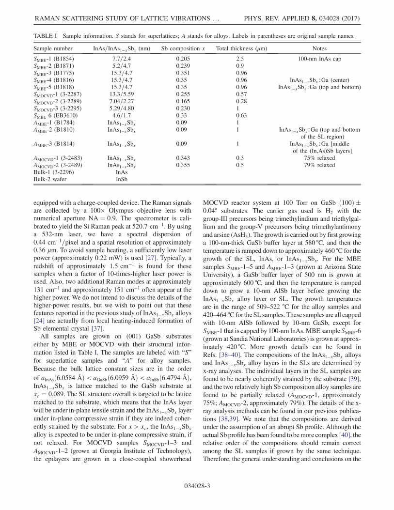
TABLE I Sample information. S stands for superlattices; A stands for alloys. Labels in parentheses are original sample names.
Sample number InAs=InAs1−xSbx (nm) Sb composition x Total thickness (μm) Notes
SMBE-1 (B1854) 7.7=2.4 0.205 2.5 100-nm InAs capSMBE-2 (B1871) 5.2=4.7 0.239 0.9SMBE-3 (B1775) 15.3=4.7 0.351 0.96SMBE-4 (B1816) 15.3=4.7 0.35 0.96 InAs1−xSbx∶Ga (center)SMBE-5 (B1818) 15.3=4.7 0.35 0.96 InAs1−xSbx∶Ga (top and bottom)SMOCVD-1 (3-2287) 13.3=5.59 0.255 0.57SMOCVD-2 (3-2289) 7.04=2.27 0.165 0.28SMOCVD-3 (3-2295) 5.29=4.80 0.230 1SMBE-6 (EB3610) 4.6=1.7 0.33 0.63AMBE-1 (B1784) InAs1−xSbx 0.09 1AMBE-2 (B1810) InAs1−xSbx 0.09 1 InAs1−xSbx∶Ga (top and bottom
of the SL region)AMBE-3 (B1814) InAs1−xSbx 0.09 1 InAs1−xSbx∶Ga [middle
of the (In,As)Sb layers]AMOCVD-1 (3-2483) InAs1−xSbx 0.343 0.3 75% relaxedAMOCVD-2 (3-2489) InAs1−xSbx 0.355 0.5 79% relaxedBulk-1 (3-2296) InAsBulk-2 wafer InSb
RAMAN SCATTERING STUDY OF LATTICE VIBRATIONS … PHYS. REV. APPLIED 8, 034028 (2017)
034028-3
SLs to be given in this work are not affected by the precisevalue of the alloy composition and profile.
III. RESULTS AND DISCUSSION
A. InAs1−xSbx alloys
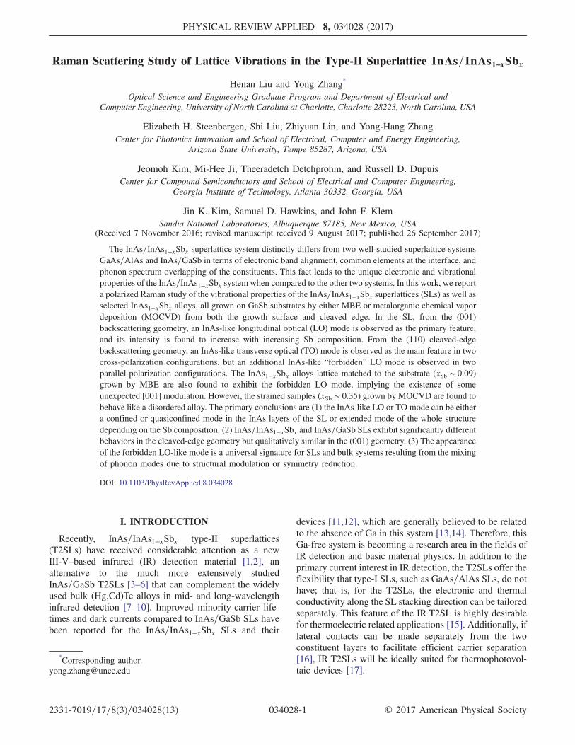
We first compare the Raman spectra of bulk InAs andInSb, as shown in Fig. 1, with Fig. 1(a) for (001) back-scattering and Fig. 1(b) for (110) backscattering. These twogeometries yield, respectively, the LO and TO phononmodes at 238.5 and 217.4 cm−1 for InAs and 190.0 and179.6 cm−1 for InSb. For both geometries, the Raman crosssections of InSb are approximately a factor of 2 larger thanthose of InAs.Figure 2 shows (001) backscattering Raman spectra for
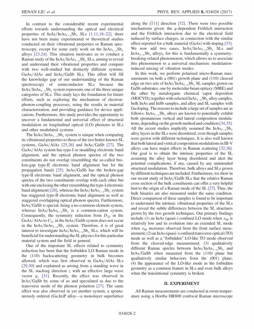
two InAs1−xSbx alloy samples: AMBE-1 with xSb ¼ 0.09 inFig. 2(a) and AMOCVD-2with xSb ¼ 0.355 in Fig. 2(b) underfour polarization configurations: zðx0; x0Þz̄, zðy0; y0Þz̄,zðx0; y0Þz̄, and zðy0; x0Þz̄. Here, we adopt the conventionsthat x0, y0, and z0 are defined as x0 ∼ ½110�, y0 ∼ ½1̄10�, andz0 ∼ ½001�, with respect to the cubic axes x ∼ ½100�,y ∼ ½010�, and z ∼ ½001�. If the alloy is viewed as havingTd symmetry on average, the two parallel-polarizationconfigurations are equivalent and both are allowed forthe LO-like phonons, and two cross-polarization configu-rations are forbidden. Indeed, the alloy samples seem toobey the selection rules (Table II) for Td symmetry in thisscattering geometry. The primary peak in both alloysamples should be the InAs-like LO mode (LO1), althoughfor the higher-xSb samples, an InSb-like LO mode (LO2) isalso observed, as reported previously for InAs1−xSbx alloys[24]. However, AMBE-1 exhibits a small anisotropy inintensity (approximately 20%) between [110] and ½1̄10�,indicating lower symmetry than Td.Figure 3 shows the comparison between the Raman
frequencies of the LO1 mode from our alloy samplesand the composition dependence of the LO1 mode for
fully relaxed alloys given in the previous report [24]:LO1ðcm−1Þ ¼ 238.5–32 xSb (replacing the xSb ¼ 0 valuewith the current room-temperature value). Apparently, theobserved LO1 frequency of approximately 229 cm−1 forthe xSb ¼ 0.355 sample lies above the curve for fullyrelaxed alloys but significantly lower than the predictedcurve for alloys under coherency strain with the substrate(the calculation is described later). The comparison indi-cates that the epitaxial layers are partially relaxed, which isconsistent with the XRD analysis, suggesting that samplesAMOCVD-1 and AMOCVD-2 are, respectively, 75% and 79%relaxed.The (110) backscattering spectra are shown in Fig. 4 in
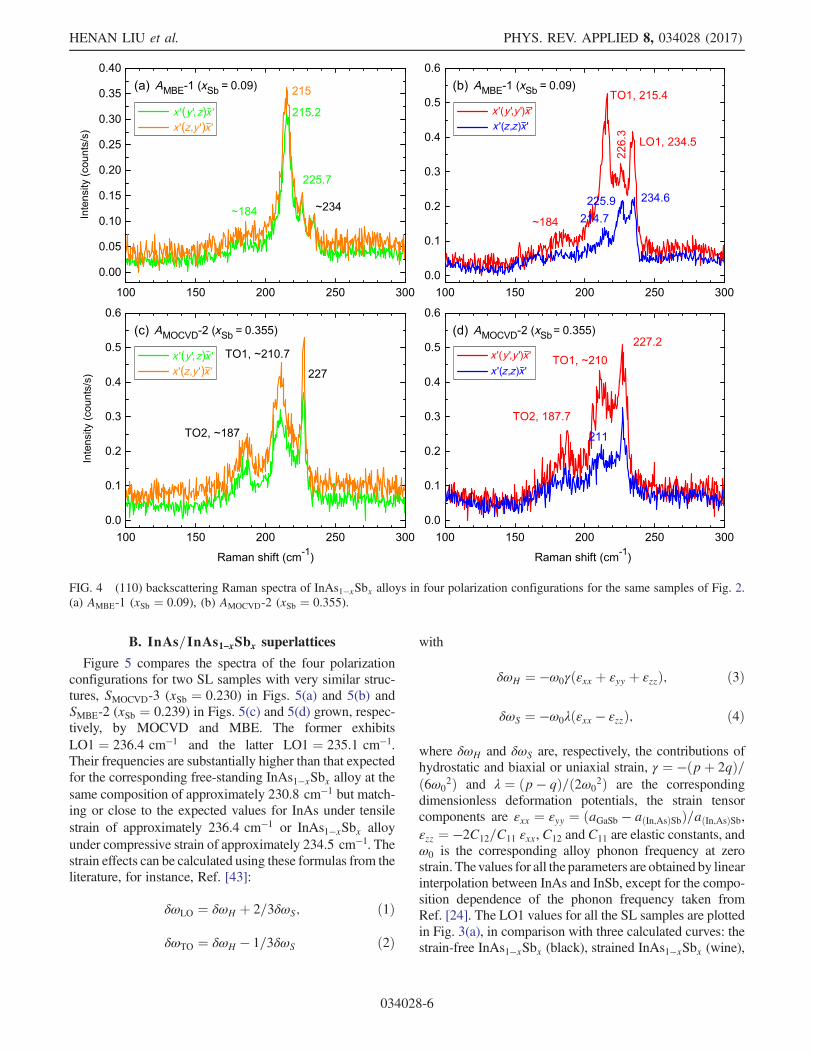
four polarization configurations for the same two alloysamples used in Fig. 2. In Td symmetry, the TO mode isforbidden in (001) backscattering but allowed in (110)backscattering [41]. However, in the previous report, the(In,As)Sb TO modes were actually measured from (001)backscattering due to the relaxation of the symmetryselection rule in an alloy but only in a range of xSb ≤0.23 [24]. Now, we are able to examine the TO modesdirectly in (110) backscattering. For Td symmetry, the threeconfigurations x0ðy0; zÞx̄0, x0ðz; y0Þx̄0, and x0ðy0; y0Þx̄0 areallowed and equivalent, and x0ðz; zÞx̄0 is forbidden (seeTable II) [41]. We note that despite the three allowedconfigurations being equivalent in Td, x0ðy0; zÞx̄0 andx0ðz; y0Þx̄0 are associated with the vibrations in the x-yplane, while x0ðy0; y0Þx̄0 is associated with the vibrationsalong the z direction. Therefore, any modulation along the zdirection, for instance, in a SL, will make x0ðy0; y0Þx̄0different from the other two. For the alloy sample, thethree configurations should remain equivalent in the idealsituation. For the alloy sample AMBE-1 with xSb ¼ 0.09,as shown in Fig. 4(a), the x0ðy0; zÞx̄0 and x0ðz; y0Þx̄0
FIG. 1 Raman spectra of bulk InAs and InSb. (a) (001) back-scattering, (b) (110) backscattering.
FIG. 2 (001) backscatteringRaman spectra of InAs1−xSbx alloysin four polarization configurations. (a) AMBE-1 (xSb ¼ 0.09),(b) AMOCVD-2 (xSb ¼ 0.355).
HENAN LIU et al. PHYS. REV. APPLIED 8, 034028 (2017)
034028-4

configurations are indeed very similar as expected. Theprimary Raman mode at approximately 215.5 cm−1 shouldbe the InAs-like TO mode (TO1) of the InAs1−xSbx alloy[24]. The weak peak at approximately 226 cm−1 is the TO
mode of the GaSb substrate because the epilayer isrelatively thin compared to the laser spot size. However,interestingly, the x0ðy0; y0Þx̄0 configuration in Fig. 4(b) turnsout to be very different from the other two, and the x0ðz; zÞx̄0configuration is also not as weak as one expects. Morepeculiar is the appearance of a Raman mode at approx-imately 234.5 cm−1, close to the LO1 mode that isobserved in (001) backscattering. Thus, although thissample is supposed to be an alloy, it behaves more likea superlattice with some sort of modulation along the [001]direction. We note that the same peak is also observed in thetwo Ga-doped samples (AMBE-2 and AMBE-3) but weakerrelative to TO1. We come back to discuss the origin of thismode later when presenting the similar phenomenonobserved in the SLs.For the alloy sample AMOCVD-2 with xSb ¼ 0.355, as
shown in Figs. 4(c) and 4(d), in contrast to the lower-xSbsample AMBE-1, this sample behaves more like a bulkmaterial of Td symmetry, and interestingly, the LO1 peakis absent. The Raman mode at approximately 211 cm−1 canbe assigned as TO1 and the other one at approximately187 cm−1 can be the InSb-like TO mode (TO2) of the alloy,which was not found previously [24]. The TO1 modefrequencies for the alloys are plotted in Fig. 3(b) comparingto the composition dependence of Ref. [24]: TO1ðcm−1Þ ¼217.4–27 xSb for xSb ≤ 0.23 (replacing the xSb ¼ 0 valuewith the current room-temperature value). The contrastbetween the two samples does not appear to be incidentalbecause the three lower-xSb samples (see Table I) behavequalitatively the same (more discussions are given later), andthe two high-xSb samples are also found to be similar.However, we cannot simply attribute the difference to thecomposition dependence because one set of samples isgrown by MBE, while the other by MOCVD. It is wellknown that different types of composition modulations mayoccur in III-Valloys, and the specific form of the modulationdepends sensitively on the growth method and condition[42]. Therefore, more systematic investigation is required tounderstand the microscopic structures of the alloys.
TABLE II Raman selection rules forD2d and Td Raman modes in (001) and (110) backscattering geometries. The notations x, y, x0, y0,and z refer to x ∼ ½100�, y ∼ ½010�, x0 ∼ ½110�, y0 ∼ ½1̄10�, and z ∼ ½001�, respectively.Symmetry group D2d Td
Symmetry
Geometry EðxÞ E (y) B2ðzÞ A1 F2ðxÞ F2ðyÞ F2ðzÞzðx0; x0Þz̄ 0 0 d2LO a2LO 0 0 d2LOzðy0; y0Þz̄ 0 0 d2LO a2LO 0 0 d2LOzðx0; y0Þz̄ 0 0 0 0 0 0 0zðy0; x0Þz̄ 0 0 0 0 0 0 0x0ðy0; y0Þx̄0 0 0 d2TO a2TO 0 0 d2TOx0ðz; zÞx̄0 0 0 0 b2TO 0 0 0x0ðy0; zÞx̄0 e2TO=2 e2TO=2 0 0 d2TO=2 d2TO=2 0x0ðz; y0Þx̄0 e2TO=2 e2TO=2 0 0 d2TO=2 d2TO=2 0
FIG. 3 Sb composition dependence of phonon frequency:(a) for the InAs-like LO phonon, (b) for the InAs-like TOphonon calculated for alloys with and without strain (solid lines)and for strained InAs (dashed lines), and measured (symbols) foralloys (circular points) and superlattices (square points).
RAMAN SCATTERING STUDY OF LATTICE VIBRATIONS … PHYS. REV. APPLIED 8, 034028 (2017)
034028-5
B. InAs=InAs1−xSbx superlattices
Figure 5 compares the spectra of the four polarizationconfigurations for two SL samples with very similar struc-tures, SMOCVD-3 (xSb ¼ 0.230) in Figs. 5(a) and 5(b) andSMBE-2 (xSb ¼ 0.239) in Figs. 5(c) and 5(d) grown, respec-tively, by MOCVD and MBE. The former exhibitsLO1 ¼ 236.4 cm−1 and the latter LO1 ¼ 235.1 cm−1.Their frequencies are substantially higher than that expectedfor the corresponding free-standing InAs1−xSbx alloy at thesame composition of approximately 230.8 cm−1 but match-ing or close to the expected values for InAs under tensilestrain of approximately 236.4 cm−1 or InAs1−xSbx alloyunder compressive strain of approximately 234.5 cm−1. Thestrain effects can be calculated using these formulas from theliterature, for instance, Ref. [43]:
δωLO ¼ δωH þ 2=3δωS; ð1Þ
δωTO ¼ δωH − 1=3δωS ð2Þ
with
δωH ¼ −ω0γðεxx þ εyy þ εzzÞ; ð3Þ
δωS ¼ −ω0λðεxx − εzzÞ; ð4Þ
where δωH and δωS are, respectively, the contributions ofhydrostatic and biaxial or uniaxial strain, γ ¼ −ðpþ 2qÞ=ð6ω0
2Þ and λ ¼ ðp − qÞ=ð2ω02Þ are the corresponding
dimensionless deformation potentials, the strain tensorcomponents are εxx ¼ εyy ¼ ðaGaSb − aðIn;AsÞSbÞ=aðIn;AsÞSb,εzz ¼ −2C12=C11 εxx, C12 andC11 are elastic constants, andω0 is the corresponding alloy phonon frequency at zerostrain. Thevalues for all the parameters are obtained by linearinterpolation between InAs and InSb, except for the compo-sition dependence of the phonon frequency taken fromRef. [24]. The LO1 values for all the SL samples are plottedin Fig. 3(a), in comparison with three calculated curves: thestrain-free InAs1−xSbx (black), strained InAs1−xSbx (wine),
FIG. 4 (110) backscattering Raman spectra of InAs1−xSbx alloys in four polarization configurations for the same samples of Fig. 2.(a) AMBE-1 (xSb ¼ 0.09), (b) AMOCVD-2 (xSb ¼ 0.355).
HENAN LIU et al. PHYS. REV. APPLIED 8, 034028 (2017)
034028-6
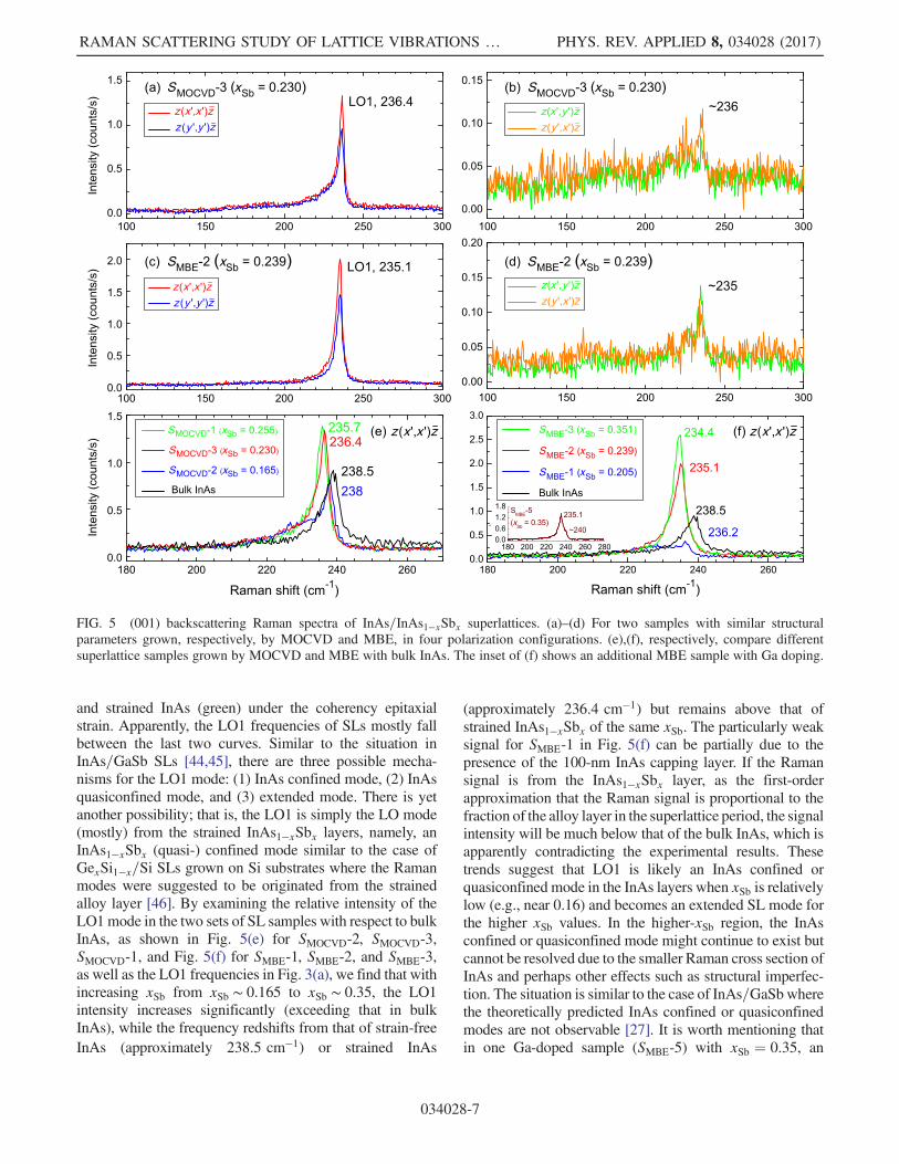
and strained InAs (green) under the coherency epitaxialstrain. Apparently, the LO1 frequencies of SLs mostly fallbetween the last two curves. Similar to the situation inInAs=GaSb SLs [44,45], there are three possible mecha-nisms for the LO1 mode: (1) InAs confined mode, (2) InAsquasiconfined mode, and (3) extended mode. There is yetanother possibility; that is, the LO1 is simply the LO mode(mostly) from the strained InAs1−xSbx layers, namely, anInAs1−xSbx (quasi-) confined mode similar to the case ofGexSi1−x=Si SLs grown on Si substrates where the Ramanmodes were suggested to be originated from the strainedalloy layer [46]. By examining the relative intensity of theLO1mode in the two sets of SL samples with respect to bulkInAs, as shown in Fig. 5(e) for SMOCVD-2, SMOCVD-3,SMOCVD-1, and Fig. 5(f) for SMBE-1, SMBE-2, and SMBE-3,as well as the LO1 frequencies in Fig. 3(a), we find that withincreasing xSb from xSb ∼ 0.165 to xSb ∼ 0.35, the LO1intensity increases significantly (exceeding that in bulkInAs), while the frequency redshifts from that of strain-freeInAs (approximately 238.5 cm−1) or strained InAs
(approximately 236.4 cm−1) but remains above that ofstrained InAs1−xSbx of the same xSb. The particularly weaksignal for SMBE-1 in Fig. 5(f) can be partially due to thepresence of the 100-nm InAs capping layer. If the Ramansignal is from the InAs1−xSbx layer, as the first-orderapproximation that the Raman signal is proportional to thefraction of the alloy layer in the superlattice period, the signalintensity will be much below that of the bulk InAs, which isapparently contradicting the experimental results. Thesetrends suggest that LO1 is likely an InAs confined orquasiconfined mode in the InAs layers when xSb is relativelylow (e.g., near 0.16) and becomes an extended SL mode forthe higher xSb values. In the higher-xSb region, the InAsconfined or quasiconfined mode might continue to exist butcannot be resolved due to the smaller Raman cross section ofInAs and perhaps other effects such as structural imperfec-tion. The situation is similar to the case of InAs=GaSbwherethe theoretically predicted InAs confined or quasiconfinedmodes are not observable [27]. It is worth mentioning thatin one Ga-doped sample (SMBE-5) with xSb ¼ 0.35, an
FIG. 5 (001) backscattering Raman spectra of InAs=InAs1−xSbx superlattices. (a)–(d) For two samples with similar structuralparameters grown, respectively, by MOCVD and MBE, in four polarization configurations. (e),(f), respectively, compare differentsuperlattice samples grown by MOCVD and MBE with bulk InAs. The inset of (f) shows an additional MBE sample with Ga doping.
RAMAN SCATTERING STUDY OF LATTICE VIBRATIONS … PHYS. REV. APPLIED 8, 034028 (2017)
034028-7
additional weaker Ramanmode at approximately 240 cm−1,close to that of InAs (approximately 238.5 cm−1), isobserved on the higher-frequency side of the main peak,as shown in the inset of Fig. 5(f). Confined or quasiconfinedmodes in the InAs1−xSbx layers are unlikely to occur unlessin a very high xSb value [44,45], which means that theobserved superlattice LO1 mode cannot be the pureInAs1−xSbx alloy mode that would be given by the strainedInAs1−xSbx curve in Fig. 3(a). This understanding isexpected to be relevant to the somewhat similar systemGexSi1−x=Si SL [47].The polarization dependence of the (001) scattering
shown in Fig. 5 indicates that the InAs=InAs1−xSbx SLobeys the Raman selection rules (see Table II) forthe SL with D2d symmetry with these four allowedRaman tensors given in the basis of (x, y, z) asA1¼½ða;0;0Þ;ð0;a;0Þ;ð0;0;bÞ�, B2ðzÞ¼ ½ð0;d;0Þ;ðd;0;0Þ;ð0;0;0Þ�, EðxÞ ¼ ½ð0; 0; 0Þ; ð0; 0; eÞ; ð0; e; 0Þ�, and EðyÞ ¼½ð0; 0; eÞ, (0,0,0), (e,0,0)] [29,48]. In general, the (001)backscattering spectra of the InAs=InAs1−xSbx SLs are
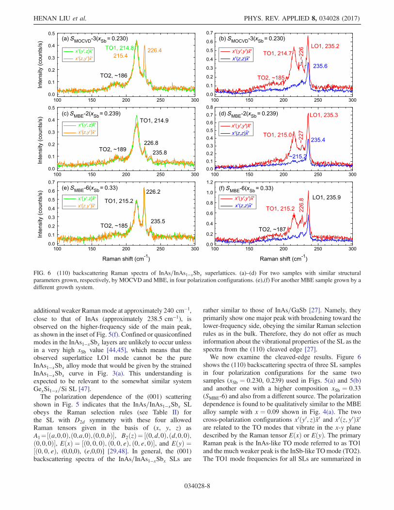
rather similar to those of InAs=GaSb [27]. Namely, theyprimarily show one major peak with broadening toward thelower-frequency side, obeying the similar Raman selectionrules as in the bulk. Therefore, they do not offer as muchinformation about the vibrational properties of the SL as thespectra from the (110) cleaved edge [27].We now examine the cleaved-edge results. Figure 6
shows the (110) backscattering spectra of three SL samplesin four polarization configurations for the same twosamples (xSb ¼ 0.230, 0.239) used in Figs. 5(a) and 5(b)and another one with a higher composition xSb ¼ 0.33(SMBE-6) and also from a different source. The polarizationdependence is found to be qualitatively similar to the MBEalloy sample with x ¼ 0.09 shown in Fig. 4(a). The twocross-polarization configurations x0ðy0; zÞx̄0 and x0ðz; y0Þx̄0are related to the TO modes that vibrate in the x-y planedescribed by the Raman tensor EðxÞ or EðyÞ. The primaryRaman peak is the InAs-like TO mode referred to as TO1and the much weaker peak is the InSb-like TOmode (TO2).The TO1 mode frequencies for all SLs are summarized in
FIG. 6 (110) backscattering Raman spectra of InAs=InAs1−xSbx superlattices. (a)–(d) For two samples with similar structuralparameters grown, respectively, by MOCVD and MBE, in four polarization configurations. (e),(f) For another MBE sample grown by adifferent growth system.
HENAN LIU et al. PHYS. REV. APPLIED 8, 034028 (2017)
034028-8
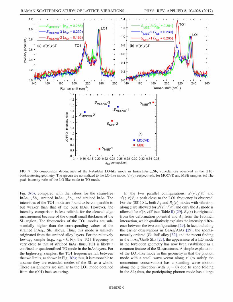
Fig. 3(b), compared with the values for the strain-freeInAs1−xSbx, strained InAs1−xSbx, and strained InAs. Theintensities of the TO1 mode are found to be comparable tobut weaker than that of the bulk InAs. However, theintensity comparison is less reliable for the cleaved-edgemeasurement because of the overall small thickness of theSL region. The frequencies of the TO1 modes are sub-stantially higher than the corresponding values of thestrained InAs1−xSbx alloys. Thus, this mode is unlikelyoriginated from the strained alloy layers. For the relativelylow-xSb sample (e.g., xSb ∼ 0.16), the TO1 frequency isvery close to that of strained InAs; thus, TO1 is likely aconfined or quasiconfined TO mode in the InAs layers. Forthe higher-xSb samples, the TO1 frequencies fall betweenthe two limits, as shown in Fig. 3(b); thus, it is reasonable toassume they are extended modes of the SL as a whole.These assignments are similar to the LO1 mode obtainedfrom the (001) backscattering.
In the two parallel configurations, x0ðy0; y0Þx̄0 andx0ðz; zÞx̄0, a peak close to the LO1 frequency is observed.For the (001) SL, both A1 and B2ðzÞ modes with vibrationalong z are allowed for x0ðy0; y0Þx̄0, and only the A1 mode isallowed for x0ðz; zÞx̄0 (see Table II) [29]. B2ðzÞ is originatedfrom the deformation potential and A1 from the Fröhlichinteraction, which qualitatively explains the intensity differ-ence between the two configurations [29]. In fact, includingthe earlier observations in GaAs=AlAs [29], the sponta-neously ordered (Ga,In)P alloy [32], and the recent findingin the InAs=GaSb SLs [27], the appearance of a LO modein the forbidden geometry has now been established as acommon feature of the SL structures. A simple explanationof the LO1-like mode in this geometry is that the phononmode with a small wave vector along x0 (to satisfy themomentum conservation) has a standing wave motionalong the z direction (with qz ¼ 0) due to zone foldingin the SL; thus, the participating phonon mode has a large
FIG. 7 Sb composition dependence of the forbidden LO-like mode in InAs=InAs1−xSbx superlattices observed in the (110)backscattering geometry. The spectra are normalized to the LO-like mode. (a),(b), respectively, for MOCVD and MBE samples. (c) Thepeak intensity ratio of the LO-like mode to TO mode.
RAMAN SCATTERING STUDY OF LATTICE VIBRATIONS … PHYS. REV. APPLIED 8, 034028 (2017)
034028-9
effective wave vector in the z direction [31]. Technically,this is a TO mode with a small SL wave vector along x0 tosatisfy the momentum conservation but with large qzcomponents of the bulk phonon modes, whereas the(001) scattering involves a LO mode with a small SLwave vector along z but, nevertheless, may have large qzcomponents of the folded bulk phonon modes. Therefore,the LOmodes observed in the two scattering configurationscan involve the similar components of the folded bulkphonon modes but with different SL wave vectors, respec-tively, along the z and x0 directions, and, thus, theirfrequencies are slightly different and can be viewed asthe longitudinal and transverse modes of the phononpolariton in the SL.Figure 7 compares the spectra of the x0ðy0; y0Þx̄0 con-
figuration normalized to LO1 for two sets of samples,SMOCVD-2, SMOCVD-3, SMOCVD-1 and SMBE-1, SMBE-2,SMBE-3, respectively, in Figs. 7(a) and 7(b), with theirpeak intensity ratios between LO1 and TO1 plotted inFig. 7(c). Interestingly, we find that the intensity ratio of theLO1 mode to the TO1 mode increases with increasing theSb composition of the InAs1−xSbx layer, which can beunderstood as due to enhanced modulation in elastic andelectronic properties with increasing contrast between theInAs and InAs1−xSbx layer. It appears that this intensityratio can serve as an empirical measure of the deviationfrom the bulk as a result of vertical structural modulation.With this understanding, we may speculate that the resultsobserved for the alloy sample with xSb ¼ 0.09 suggest thepossible existence of unintended vertical modulation.Although such modulation might not be periodic as in aSL (thus, no standing wave formation), the perturbationseems to be sufficient to induce some phonon-scatteringeffects that may also lead to the mixture of the modes withdifferent qz values. Spontaneous composition modulationalong the z axis has been reported in InAs1−xSbx alloyswith 0.4 ≤ xSb ≤ 0.8 [35], although not in such a lowcomposition. More careful structural study is required toidentify the exact nature of the modulation, but cleaved-edge-polarized Raman spectroscopy shows to be a verysensitive tool for revealing the existence of the modulation.
IV. COMPARISON BETWEEN InAs=InAs1−xSbx,InAs=GaSb, AND GaAs=AlAs SUPERLATTICES
In the (001) backscattering geometry, the selection rulesin the SLs for the four commonly adopted configurationszðx0; x0Þz̄, zðy0; y0Þz̄, zðx0; y0Þz̄, and zðy0; x0Þz̄ are usually thesame as in the bulk. It is rather unique that for GaAs=AlAsSLs, multiple confined LO modes can be observed,benefiting from their LO phonon spectra being wellseparated [49]. For both InAs=GaSb SLs [27] andInAs=InAs1−xSbx SLs (Fig. 5), there is only one primaryLO mode. Therefore, the Raman scattering results of thisgeometry are not very informative for understanding the
vibrational properties of the SLs, and no qualitativelydifference is revealed between the two systems.It is the (110) backscattering geometry that reveals some
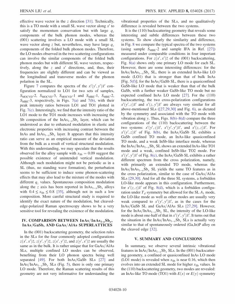
interesting and subtle differences between these twosystems. To show clearly the similarity and difference,in Fig. 8 we compare the typical spectra of the two systems(using sample SMBE-2 and sample IFA in Ref. [27])measured under comparable conditions in four importantconfigurations. For zðx0; x0Þz̄ of the (001) backscattering,Fig. 8(a) shows only one primary LO mode for each SL.However, there are some interesting differences: for theInAs=InAs1−xSbx SL, there is an extended InAs-like LOmode (LO1) that is stronger than that of bulk InAs[Fig. 5(f)]; for the InAs=GaSb SL, there is a quasiconfinedGaSb-like LO mode that is weaker than that of the bulkGaSb, with a further weaker GaSb-like TO mode but noexpected confined InAs LO mode [27]. For the (110)backscattering, the two cross-polarization configurationsx0ðy0; zÞx̄0 and x0ðz; y0Þx̄0 are always very similar for allabove-mentioned SLs ([27,29,30] and Fig. 6), as dictatedby the symmetry and associated with the TO mode withvibration along y. Thus, Figs. 8(b)–8(d) compare the threeconfigurations of the (110) backscattering between thetwo systems: x0ðy0; zÞx̄0, x0ðy0; y0Þx̄0, and x0ðz; zÞx̄0. Forx0ðy0; zÞx̄0 of Fig. 8(b), the InAs=GaSb SL exhibits aGaSb confined TO mode, an InAs-like quasiconfinedTO mode, and a weak InSb-like interface mode, whereasthe InAs=InAs1−xSbx SL shows an extended InAs-like TO1mode and a weak, confined InSb-like TO2 mode. Forx0ðy0; y0Þx̄0 of Fig. 8(c), the InAs=GaSb SL exhibits a ratherdifferent spectrum from the cross polarization, namely,with primarily an extended TO mode, whereas theInAs=InAs1−xSbx SL yields the same TO features as inthe cross polarization, similar to the case of GaAs=AlAsSLs [29,30]. And for all the three SL systems, a forbiddenLO-like mode appears in this configuration. Furthermore,for x0ðz; zÞx̄0 of Fig. 8(d), which is a forbidden configu-ration under Td symmetry but allowed for the SL A1 mode,the LO-like mode as well as other modes are usually veryweak compared to x0ðy0; y0Þx̄0, as in the cases for theInAs=GaSb SL and GaAs=AlAs SLs [27,29]. However,for the InAs=InAs1−xSbx SL, the intensity of the LO-likemode is about one-half of that in x0ðy0; y0Þx̄0. It turns out thatthe situation in the InAs=InAs1−xSbx SLs is actually verysimilar to that of spontaneously ordered (Ga,In)P alloy onthe cleaved edge [32].
V. SUMMARY AND CONCLUSIONS
In summary, we observe several intrinsic vibrationalfeatures in InAs=InAs1−xSbx SLs. In the (001) backscatter-ing geometry, a confined or quasiconfined InAs LO mode(LO1 mode) is revealed when xSb is near 0.16, which thenevolves into an extended SL mode for higher xSb values. Inthe (110) backscattering geometry, two modes are revealed:an InAs-like TO mode (TO1) with EðxÞ or EðyÞ symmetry
HENAN LIU et al. PHYS. REV. APPLIED 8, 034028 (2017)
034028-10
that also evolves from an InAs confined or quasiconfinedmode into an extended mode with increasing xSb and aLO1-like mode with A1 and B2ðzÞ symmetry.The InAs1−xSbx alloys grown by MBE with xSb lattice
matching to the GaSb substrate are found to possibly havesome structural modulation along the growth direction.Additionally, Ga-doping effects are also briefly examinedfor InAs=InAs1−xSbx SLs and InAs1−xSbx alloys. Twopreviously reported unexplained peaks in InAs1−xSbxalloys are found to be the result of unintended laser-inducedformation of Sb elemental crystal.A LO-like mode has now been established as a common
feature observable in the backscattering geometry fromthe plane containing the axis of the structural modulation,for instance, the (110) plane for a [001] superlattice as inGaAs=AlAs, InAs=GaSb, and InAs=InAs1−xSbx or the(110) plane for a CuPt-ordered (Ga,In)P along ½1̄11�direction. A unified understanding is given for all theseseemingly very different types of SLs and alloys asresulting from phonon mode mixing associated with eithera structural or a certain form of modulation that breaks the
translational symmetry. In addition, InAs=InAs1−xSbx andInAs=GaSb SLs are shown to exhibit qualitatively differentspectroscopy signatures when probed from the (110)cleaved edge but not from the (001) growth plane.Considerable variations between the InAs=InAs1−xSbx
SLs grown by different systems indicate that the structuresare far from perfect, likely with considerable thickness andcomposition fluctuations at the interfaces. This studyprovides the basic understanding of the vibrational proper-ties of this emerging material system, which provides ameaningful reference for applying Raman spectroscopy asa nondestructive characterization technique in the futurestudy of this SL system.
ACKNOWLEDGMENTS
The work at UNCC, GT, and ASU is supported by ARO/MURI (Grant No. W911NF-10-1-0524, Dr. WilliamClark). Sandia National Laboratories is a multimissionlaboratory managed and operated by National Technologyand Engineering Solutions of Sandia LLC, a wholly ownedsubsidiary of Honeywell International Inc. for the U.S.
FIG. 8 Comparison between InAs=InAs1−xSbx and InAs=GaSb superlattices: (a) for (001) backscattering, (b)–(d) for (110)backscattering in three polarization configurations. The peak indicated by “star” is from the GaSb substrate in the spectra for theInAs=InAs1−xSbx superlattice.
RAMAN SCATTERING STUDY OF LATTICE VIBRATIONS … PHYS. REV. APPLIED 8, 034028 (2017)
034028-11
Department of Energy’s National Nuclear SecurityAdministration under contract DE-NA0003525. Y. Z.thanks Dr. Andrew Norman of NREL for very helpfuldiscussions and acknowledges the support of BissellDistinguished Professorship at UNCC.
[1] D. Zuo, R. Liu, D. Wasserman, J. Mabon, Z.-Y. He, S. Liu,Y.-H. Zhang, E. A. Kadlec, B. V. Olson, and E. A. Shaner,Direct minority carrier transport characterization ofInAs=InAsSb superlattice nBn photodetectors, Appl. Phys.Lett. 106, 071107 (2015).
[2] Z.-D. Ning, S.-M. Liu, S. Luo, F. Ren, F. Wang, T. Yang,F.-Q. Liu, Z.-G. Wang, and L.-C. Zhao, Growth andcharacterization of InAs=InAsSb superlattices by metalorganic chemical vapor deposition for mid-wavelengthinfrared photodetectors, Mater. Lett. 164, 213 (2016).
[3] B. Olson, L. Murray, J. Prineas, M. Flatté, J. Olesberg, andT. Boggess, All-optical measurement of vertical chargecarrier transport in mid-wave infrared InAs=GaSb type-IIsuperlattices, Appl. Phys. Lett. 102, 202101 (2013).
[4] E. A. Plis, M. N. Kutty, and S. Krishna, Passivation tech-niques for InAs=GaSb strained layer superlattice detectors,Laser Photonics Rev. 7, 45 (2013).
[5] G. Chen, A. Hoang, S. Bogdanov, A. Haddadi, P. Bijjam,B.-M. Nguyen, and M. Razeghi, Investigation of impuritiesin type-II InAs=GaSb superlattices via capacitance-voltagemeasurement, Appl. Phys. Lett. 103, 033512 (2013).
[6] N. Baril, S. Bandara, L. Hoeglund, N. Henry, A. Brown,C. Billman, P. Maloney, E. Nallon, M. Tidrow, and J.Pellegrino, Low operating bias InAs=GaSb strain layersuperlattice LWIR detector, Infrared Phys. Technol. 70,58 (2015).
[7] C. H. Grein, P. M. Young, M. E. Flatte, and H. Ehrenreich,Long wavelength InAs=InGaSb infrared detectors: Optimi-zation of carrier lifetimes, J. Appl. Phys. 78, 7143 (1995).
[8] P. Manurkar, S. Ramezani-Darvish, B.-M. Nguyen, M.Razeghi, and J. Hubbs, High performance long wavelengthinfrared mega-pixel focal plane array based on type-IIsuperlattices, Appl. Phys. Lett. 97, 193505 (2010).
[9] D. L. Smith and C. Mailhiot, Proposal for strained type IIsuperlattice infrared detectors, J. Appl. Phys. 62, 2545(1987).
[10] E. R.Youngdale, J. R.Meyer,C. A.Hoffman,F. J.Bartoli,C. H.Grein, P. M. Young, H. Ehrenreich, R. H. Miles, and D. H.Chow, Auger lifetime enhancement in InAs-Ga1−xInxSbsuperlattices, Appl. Phys. Lett. 64, 3160 (1994).
[11] E. H. Steenbergen, B. C. Connelly, G. D. Metcalfe, H. Shen,M. Wraback, D. Lubyshev, Y. Qiu, J. M. Fastenau, A. W. K.Liu, S. Elhamri, O. O. Cellek, and Y. H. Zhang, Signifi-cantly improved minority carrier lifetime observed in a long-wavelength infrared III-V type-II superlattice comprised ofInAs=InAsSb, Appl. Phys. Lett. 99, 251110 (2011).
[12] H. S. Kim, O. O. Cellek, Z.-Y. Lin, Z.-Y. He, X.-H. Zhao, S.Liu, H. Li, and Y.-H. Zhang, Long-wave infrared nBnphotodetectors based on InAs=InAsSb type-II superlattices,Appl. Phys. Lett. 101, 161114 (2012).
[13] G. Belenky, G. Kipshidze, D. Donetsky, S. P. Svensson,W. L. Sarney, H. Hier, L. Shterengas, D. Wang, and
Y. Lin, in Infrared Technology and Applications, edited byB. F. Andresen, G. F. Fulop, and P. R. Norton, SPIEProceedings Vol. XXXVII (SPIE-International Society forOptical Engineering, Bellingham, WA, 2011).
[14] S. P. Svensson, D. Donetsky, D. Wang, H. Hier, F. J.Crowne, and G. Belenky, Growth of type II strained layersuperlattice, bulk InAs and GaSb materials for minoritylifetime characterization, J. Cryst. Growth 334, 103(2011).
[15] G. D. Mahan and J. O. Sofo, The best thermoelectric, Proc.Natl. Acad. Sci. U.S.A. 93, 7436 (1996).
[16] Y. Zhang, L.-W. Wang, and A. Mascarenhas, “Quantumcoaxial cables” for solar energy harvesting, Nano Lett. 7,1264 (2007).
[17] T. Bauer, Thermophotovoltaics (Springer, New York, 2011).[18] E. Plis, T. Schuler-Sandy, D. Ramirez, S. Myers, and S.
Krishna, Dark current reduction in InAs=InAsSb super-lattice mid-wave infrared detectors through restoration etch,Electron. Lett. 51, 2009 (2015).
[19] L. Höglund, D. Z. Ting, A. Khoshakhlagh, A. Soibel, C. J.Hill, A. Fisher, S. Keo, and S. D. Gunapala, Influence ofradiative and non-radiative recombination on the minoritycarrier lifetime in midwave infrared InAs=InAsSb super-lattices, Appl. Phys. Lett. 103, 221908 (2013).
[20] Y. Aytac, B. V. Olson, J. K. Kim, E. A. Shaner, S. D.Hawkins, J. F. Klem, J. Olesberg, M. E. Flatté, and T. F.Boggess, Bandgap and temperature dependence of Augerrecombination in InAs=InAsSb type-II superlattices, J. Appl.Phys. 119, 215705 (2016).
[21] Y. Aytac, B. V. Olson, J. K. Kim, E. A. Shaner, S. D.Hawkins, J. F. Klem, M. E. Flatté, and T. F. Boggess,Evidence of a Shockley-Read-Hall Defect State Indepen-dent of Band-Edge Energy in InAs=InðAs; SbÞ Type-IISuperlattices, Phys. Rev. Applied 5, 054016 (2016).
[22] B. V. Olson, J. F. Klem, E. A. Kadlec, J. K. Kim, M. D.Goldflam, S. D. Hawkins, A. Tauke-Pedretti, W. T. Coon,T. R. Fortune, E. A. Shaner, and M. E. Flatté, Vertical HoleTransport and Carrier Localization in InAs=InAs1−xSbxType-II Superlattice Heterojunction Bipolar Transistors,Phys. Rev. Applied 7, 024016 (2017).
[23] Y. T. Cherng, K. Y. Ma, and G. B. Stringfellow, Raman-scattering in InAs1−xSbx grown by organometallic vapor-phase epitaxy, Appl. Phys. Lett. 53, 886 (1988).
[24] Y. B. Li, S. S. Dosanjh, I. T. Ferguson, A. G. Norman, A. G.Deoliveira, R. A. Stradling, and R. Zallen, Raman-scatteringin InAs1−xSbx alloys grown in GaAs by molecular-beamepitaxy, Semicond. Sci. Technol. 7, 567 (1992).
[25] D. Berdekas and S. Ves, Lattice dynamics and Ramanscattering by phonons of GaAs=AlAs (001) superlattices,J. Phys. Condens. Matter 21, 275405 (2009).
[26] J. Menéndez, Phonons in GaAs-AlxGa1−xAs superlattices,J. Lumin. 44, 285 (1989).
[27] H. Liu, N. Yue, Y. Zhang, P. Qiao, D. Zuo, B. Kesler, S. L.Chuang, J.-H. Ryou, J. D. Justice, and R. Dupuis, Latticevibration modes in type-II superlattice InAs=GaSb with no-common-atom interface and overlapping vibration spectra,Phys. Rev. B 91, 235317 (2015).
[28] A. Fasolino, E. Molinari, and J. C. Maan, Calculatedsuperlattice and interface phonons of InAs=GaSb super-lattices, Phys. Rev. B 33, 8889 (1986).
HENAN LIU et al. PHYS. REV. APPLIED 8, 034028 (2017)
034028-12
[29] A. Fainstein, P. Etchegoin, M. P. Chamberlain, M. Cardona,K. Totemeyer, and K. Eberl, Selection rules and dispersion ofGaAs=AlAs multiple-quantum-well optical phonons studiedby Raman scattering in right-angle, forward, and backscatter-ing in-plane geometries, Phys. Rev. B 51, 14448 (1995).
[30] R. Hessmer, A. Huber, T. Egeler, M. Haines, G. Tränkle, G.Weimann, and G. Abstreiter, Interface-phonon dispersionand confined-optical-mode selection rules of GaAs=AlAssuperlattices studied by micro-Raman spectroscopy, Phys.Rev. B 46, 4071 (1992).
[31] B. Jusserand and M. Cardona, in Light Scattering in Solids,edited by M. Cardona and G. Güntherodt (Springer, Berlin,1989), p. 49.
[32] A. Mascarenhas, H. Cheong, and F. Alsina, in SpontaneousOrdering in Semiconductor Alloys, edited byA.Mascarenhas(Kluwer Academy, New York, 2002), p. 391.
[33] F. Schäffler and G. Abstreiter, Electric-field-induced Ramanscattering: Resonance, temperature, and screening effects,Phys. Rev. B 34, 4017 (1986).
[34] A. G. Norman, T. Y. Seong, I. T. Ferguson, G. R. Booker,and B. A. Joyce, Structural studies of natural superlattices ingroup III-V alloy epitaxial layers, Semicond. Sci. Technol.8, S9 (1993).
[35] T. Y. Seong, A. G. Norman, I. T. Ferguson, and G. R.Booker, Transmission electron microscopy and transmis-sion electron diffraction structural studies of heteroepitaxialInAsySb1−y molecular-beam epitaxial layers, J. Appl. Phys.73, 8227 (1993).
[36] H. M. Cheong, Y. Zhang, A. G. Norman, J. D. Perkins, A.Mascarenhas, K. Y. Cheng, and K. C. Hsieh, ResonanceRaman scattering studies of composition-modulatedGaP=InP short-period superlattices, Phys. Rev. B 60,4883 (1999).
[37] R. L. Farrow, R. K. Chang, S. Mroczkowski, and F. H.Pollak, Detection of excess crystalline As and Sb in III-Voxide interfaces by Raman scattering, Appl. Phys. Lett. 31,768 (1977).
[38] E. H. Steenbergen, Y. Huang, J. H. Ryou, L. Ouyang, J. J.Li, D. J. Smith, R. D. Dupuis, and Y. H. Zhang, Structural
and optical characterization of type-II InAs=InAs1−xSbxsuperlattices grown by metalorganic chemical vapor depo-sition, Appl. Phys. Lett. 99, 071111 (2011).
[39] E. H. Steenbergen, K. Nunna, L. Ouyang, B. Ullrich, D. L.Huffaker, D. J. Smith, and Y.-H. Zhang, Strain-balancedInAs=InAs1−xSbx type-II superlattices grown by molecularbeam epitaxy on GaSb substrates, J. Vac. Sci. Technol. B 30,02B107 (2012).
[40] M. R. Wood, K. Kanedy, F. Lopez, M. Weimer, J. F. Klem,S. D. Hawkins, E. A. Shaner, and J. K. Kim, Monolayer-by-monolayer compositional analysis of InAs=InAsSb super-lattices with cross-sectional STM, J. Cryst. Growth 425, 110(2015).
[41] P. Yu and M. Cardona, Fundamentals of Semiconductors(Springer, New York, 2010).
[42] A. Mascarenhas, Spontaneous Ordering in SemiconductorAlloys (Kluwer Academic/Plenum Publishers, New York,2002).
[43] B. Jusserand, P. Voisin, M. Voos, L. L. Chang, E. E.Mendez, and L. Esaki, Raman scattering in GaSb-AlSbstrained layer superlattices, Appl. Phys. Lett. 46, 678(1985).
[44] A. Fasolino, E. Molinari, and J. C. Maan, Resonant quasi-confined optical phonons in semiconductor superlattices,Phys. Rev. B 39, 3923 (1989).
[45] D. Berdekas and G. Kanellis, Phonon confinement inInAs=GaSb superlattices, Phys. Rev. B 43, 9976 (1991).
[46] F. Cerdeira, A. Pinczuk, J. C. Bean, B. Batlogg, and B. A.Wilson, Raman scattering from GexSi1−x=Si strained-layersuperlattices, Appl. Phys. Lett. 45, 1138 (1984).
[47] H. K. Shin, D. J. Lockwood, and J. M. Baribeau, Strain incoherent-wave SiGe/Si superlattices, Solid State Commun.114, 505 (2000).
[48] R. Loudon, Raman effect in crystals, Adv. Phys. 13, 423(1964).
[49] A. K. Sood, J. Menéndez, M. Cardona, and K. Ploog,Resonance Raman Scattering by Confined LO and TOPhonons in GaAs-AlAs Superlattices, Phys. Rev. Lett. 54,2111 (1985).
RAMAN SCATTERING STUDY OF LATTICE VIBRATIONS … PHYS. REV. APPLIED 8, 034028 (2017)
034028-13