Embed Size (px)
Citation preview
RAK831 Datasheet
COPYRIGHT ©
SHENZHEN RAKWIRELESS TECHNOLOGY CO., LTD
www.rakwireless.com
1
RAK831 Lora Gateway
Datasheet - RUS V1.3
(RAK831 LoRa/LoRaWAN Gateway Module, base on SX1301, 433/868/915MHz,range of up to 49200ft, Wireless Spread Spectrum Transmission)
© 2017 Rakwireless all rights reserved .
Mentioned in this document , the actual company and product
names, trademarks are their respective owners.
After update the new version, this document without prior notice.
RAK831 Datasheet
COPYRIGHT ©
SHENZHEN RAKWIRELESS TECHNOLOGY CO., LTD
www.rakwireless.com
2
Content
Content ..........................................................................................................................................2
1. Introduction ................................................................................................................................3 1.1 Key Features ........................................................................................................................................ 4
1.2 Applications .......................................................................................................................................... 4
2.Module Package ............................................................................................................................5 2.1 Pinout Description .................................................................................................................................. 5
2.2 Module Dimensions ................................................................................................................................ 6
3.Module Overview .........................................................................................................................7 3.1 SX1301 ................................................................................................................................................... 7
3.1.1 Block Diagram ...................................................................................................................................... 8
3.1.2 IF8 LORA channel ............................................................................................................................... 8
3.1.3 IF9 (G) FSK channel ............................................................................................................................ 9
3.1.4 IF0 to IF7 LORA channels ................................................................................................................... 9
3.3 External Module Connector .................................................................................................................. 10 3.3.1 SPI ...................................................................................................................................................... 10
3.3.2 GPS PPS ............................................................................................................................................. 10
3.3.3 Digital IOs .......................................................................................................................................... 10
4.LoRa Systems, Network Approach ............................................................................................. 11 4.1 Overview ............................................................................................................................................... 11
4.2 Firmware ................................................................................................................................................ 11
5.Electrical Characteristics&Timing specifications .......................................................................12 5.1 Absolute Maximum Ratings ................................................................................................................. 12
5.2 Global Electrical Characteristics .......................................................................................................... 12
5.3 SPI Interface Characteristics ................................................................................................................ 13
5.4 RF Characteristics................................................................................................................................. 13 5.4.1 Transmitter RF Characteristics ........................................................................................................... 13
5.4.2 Receiver RF Characteristics ................................................................................................................ 14
5.5. RF Key Components ....................................................................................................................... 14
5.6. RF antenna interface ....................................................................................................................... 15
6.Ordering Information ..................................................................................................................17
7. Contact information ...................................................................................................................18
8.Appendix .....................................................................................................................................19
9. Change Note ..............................................................................................................................20
RAK831 Datasheet
COPYRIGHT ©
SHENZHEN RAKWIRELESS TECHNOLOGY CO., LTD
www.rakwireless.com
3
1.Introduction
The concentrator module RAK831 is targeted for a huge variety of applications like Smart
Metering, IoT and M2M applications. It is a multi- channel high performance Transmitter/receiver
module designed to receive several LoRa packets simultaneously using different spreading factors
on multiple channels. The concentrator module RAK831 can be integrated into a gateway as a
complete RF front end of this gateway. It provides the possibility to enable robust communication
between a LoRa gateway and a huge amount of LoRa end-nodes spread over a wide range of
distance. The RAK831 needs a host system for proper operation.
This is a ideal modular products to help you realize the whole Lora system development. With the
USB-SPI converter module FT2232, you can quickly to make the software development in your PC. But
also, you can integrate the concentrator module to your production product to realize the Lora gateway
function.This is very economic way to address for a huge variety of applications like Smart Grid, Intelligent
Farm,intelligent Farm and Other IoT applications.
The RAK831 needs a host system like Raspberry Pi or WisAP(OpenWRT based) or WisCam for
proper operation . The host processor can be a PC or MCU that will be connected to RAK831 via USB or
SPI
RAK831 is able to receive up to 8 LoRa packets simultaneously sent with different spreading
factors on different channels. This unique capability allows to implement innovative network
architectures advantageous over other short range systems:
End-point nodes (e.g. sensor nodes) can change frequency with each transmission in a random
pattern. This provides vast improvement of the system robustness in term s of interferer immunity
and radio channel diversity.
RAK831 Datasheet
COPYRIGHT ©
SHENZHEN RAKWIRELESS TECHNOLOGY CO., LTD
www.rakwireless.com
4
1.1 Key Features
- Compact size 80.0 x 50.0 x 5.0mm
- LoRaTM modulation technology
- Frequency band 433,470, 868,915MHz
- Orthogonal spreading factors
- Sensitivity down to -142.5 dBm
- Maximum link budget162 dB
- SPI interface
- SX1301 base band processor
- Emulates 49 x LoRa demodulators
- 12 parallel demodulation paths
- 1 (G)FSK demodulator
- 2 x SX1257 Tx/Rx front-ends High frequency
- 2 x SX1255 Tx/Rx front-ends low frequency
- Supply voltage 5 V
- RF interface optimized to 50
- Output power level up to 23 dBm
- GPS receiver (optional)
- Range up to 15 km (Line of Sight)
- Range of several km in urban environment
- Status LEDs
- HAL is available from
https://github.com/RAKWireless/RAK831_LoRaGateway
1.2 Applications
- Smart Metering
- Wireless Star Networks
-.Home,Building,Industrial automation
- Remote Control
- Wireless Sensors
- M2M, IoT
- Wireless Alarm and Security Systems
- …
RAK831 Datasheet
COPYRIGHT ©
SHENZHEN RAKWIRELESS TECHNOLOGY CO., LTD
www.rakwireless.com
5
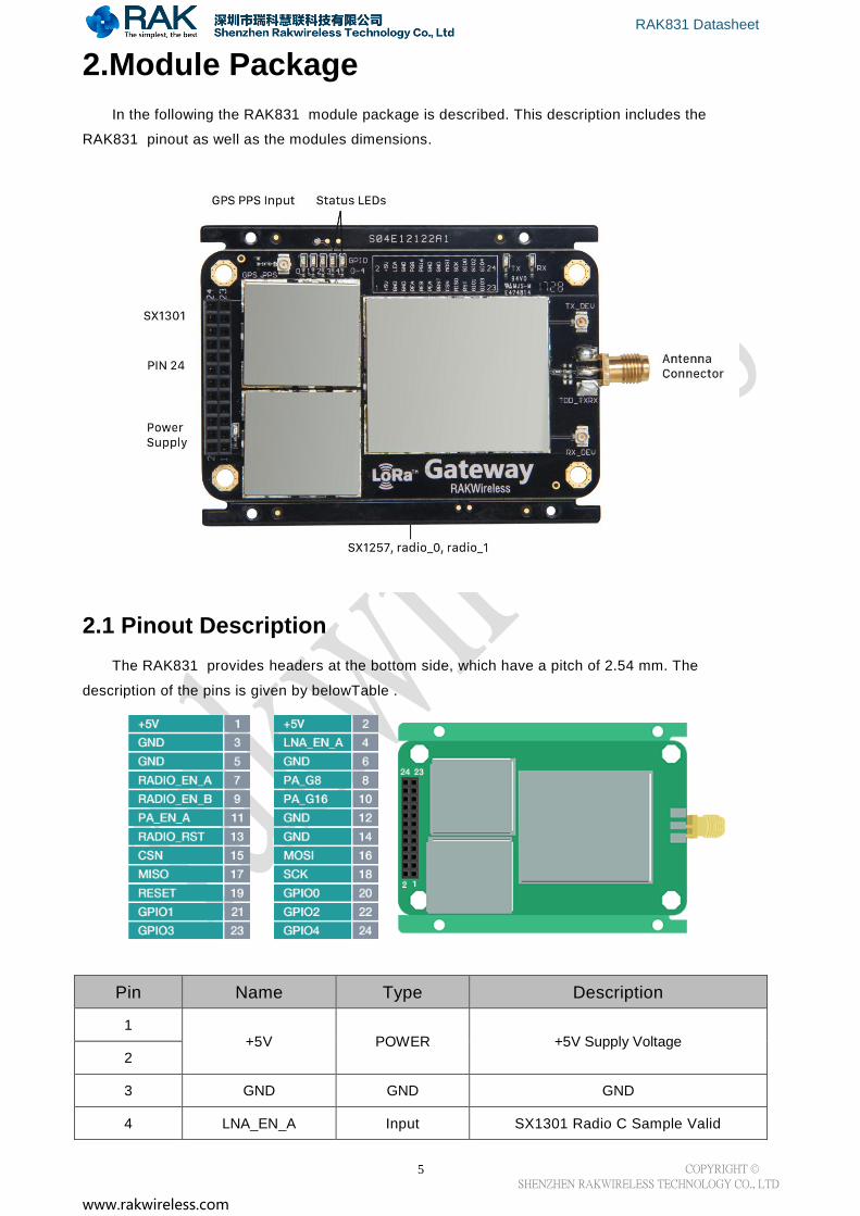
2.Module Package
In the following the RAK831 module package is described. This description includes the
RAK831 pinout as well as the modules dimensions.
2.1 Pinout Description
The RAK831 provides headers at the bottom side, which have a pitch of 2.54 mm. The
description of the pins is given by belowTable .
Pin Name Type Description
1 +5V POWER +5V Supply Voltage
2
3 GND GND GND
4 LNA_EN_A Input SX1301 Radio C Sample Valid
RAK831 Datasheet
COPYRIGHT ©
SHENZHEN RAKWIRELESS TECHNOLOGY CO., LTD
www.rakwireless.com
6
5 GND GND GPS Module LDO:Enable Pin
6 GND GND GND
7 RADIO_EN_A Input SX1257_A_EN
8 PA_G8 Input PA GAIN 0
9 RADIO_EN_B Input SX1257_B_EN
10 PA_G16 Input PA GAIN 1
11 PA_EN_A Input PA EN
12 GND GND GND
13 RADIO_RST RST SX1257_A_B RESET
14 GND GND GND
15 CSN SPI SX1301 SPI_NSS
16 MOSI SPI SX1301 SPI_MOSI
17 MISO SPI SX1301 SPI_MISO
18 SCK SPI SX1301 SPI_CLK
19 RESET RST SX1301 RESET
20 GPIO0 GPIO SX1301 GPIO
21 GPIO1 GPIO SX1301 GPIO
22 GPIO2 GPIO SX1301 GPIO
23 GPIO3 GPIO SX1301 GPIO
24 GPIO4 GPIO SX1301 GPIO
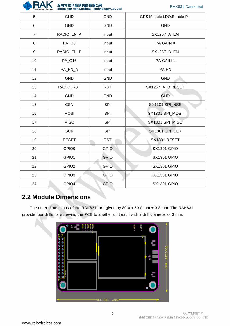
2.2 Module Dimensions
The outer dimensions of the RAK831 are given by 80.0 x 50.0 mm ± 0.2 mm. The RAK831
provide four drills for screwing the PCB to another unit each with a drill diameter of 3 mm.
RAK831 Datasheet
COPYRIGHT ©
SHENZHEN RAKWIRELESS TECHNOLOGY CO., LTD
www.rakwireless.com
7
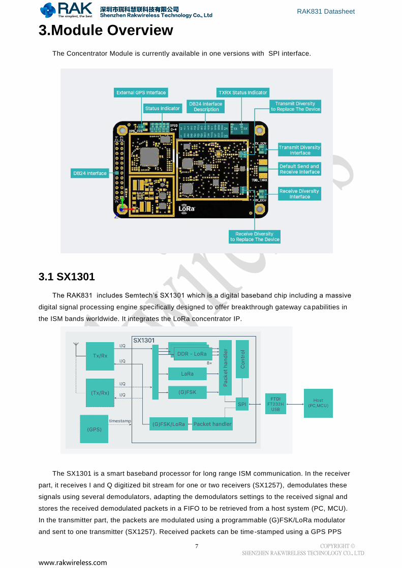
3.Module Overview
The Concentrator Module is currently available in one versions with SPI interface.
3.1 SX1301
The RAK831 includes Semtech’s SX1301 which is a digital baseband chip including a massive
digital signal processing engine specifically designed to offer breakthrough gateway capabilities in
the ISM bands worldwide. It integrates the LoRa concentrator IP.
The SX1301 is a smart baseband processor for long range ISM communication. In the receiver
part, it receives I and Q digitized bit stream for one or two receivers (SX1257), demodulates these
signals using several demodulators, adapting the demodulators settings to the received signal and
stores the received demodulated packets in a FIFO to be retrieved from a host system (PC, MCU).
In the transmitter part, the packets are modulated using a programmable (G)FSK/LoRa modulator
and sent to one transmitter (SX1257). Received packets can be time-stamped using a GPS PPS
RAK831 Datasheet
COPYRIGHT ©
SHENZHEN RAKWIRELESS TECHNOLOGY CO., LTD
www.rakwireless.com
8
input.
The SX1301 has an internal control block that receives microcode from the host system (PC,
MCU). The microcode is provided by Semtech as a binary file to load into the SX1301 at power -on
(see Semtech application support for more information).
The control of the SX1301 by the host system (PC, MCU) is made using a Hardware
Abstraction Layer (HAL). The Hardware Abstraction Layer source code is provided by Semtech and
can be adapted by the host system developers.
It is highly recommended to fully re-use the latest HAL as provided by Semtech on
https://github.com/Lora-net.
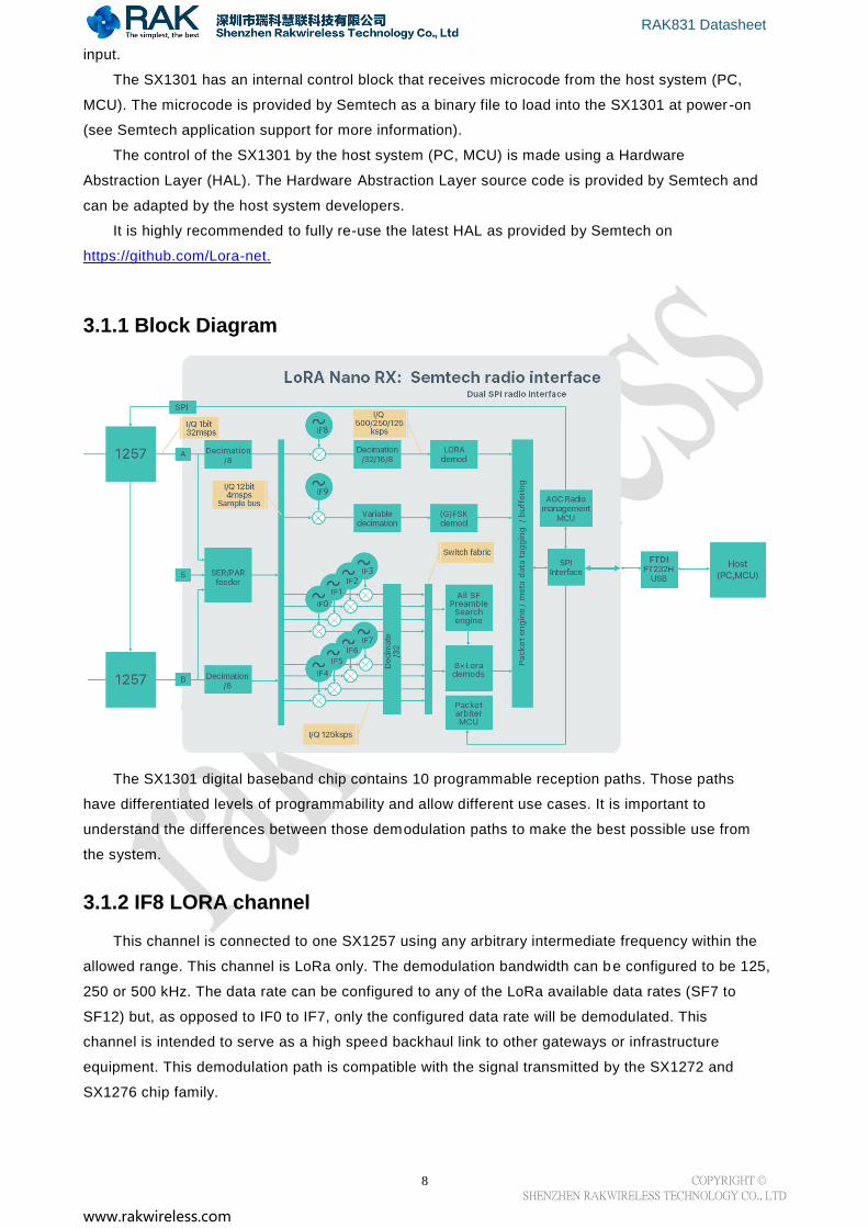
3.1.1 Block Diagram
The SX1301 digital baseband chip contains 10 programmable reception paths. Those paths
have differentiated levels of programmability and allow different use cases. It is important to
understand the differences between those demodulation paths to make the best possible use from
the system.
3.1.2 IF8 LORA channel
This channel is connected to one SX1257 using any arbitrary intermediate frequency within the
allowed range. This channel is LoRa only. The demodulation bandwidth can be configured to be 125,
250 or 500 kHz. The data rate can be configured to any of the LoRa available data rates (SF7 to
SF12) but, as opposed to IF0 to IF7, only the configured data rate will be demodulated. This
channel is intended to serve as a high speed backhaul link to other gateways or infrastructure
equipment. This demodulation path is compatible with the signal transmitted by the SX1272 and
SX1276 chip family.
RAK831 Datasheet
COPYRIGHT ©
SHENZHEN RAKWIRELESS TECHNOLOGY CO., LTD
www.rakwireless.com
9
3.1.3 IF9 (G) FSK channel
The IF9 channel is connected to a GFSK demodulator. The channel bandwidth and bit rate can
be adjusted. This demodulator offers a very high level of configurability, going well beyond the
scope of this document. The demodulator characteristics are essentially the same than the GFSK
demodulator implemented on the SX1232 and SX1272 Semtech chips. This demodulation path can
demodulate any legacy FSK or GFSK formatted signal.
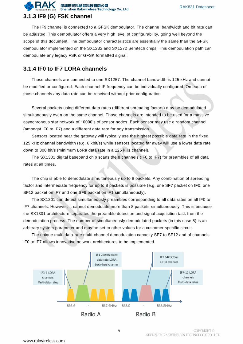
3.1.4 IF0 to IF7 LORA channels
Those channels are connected to one SX1257. The channel bandwidth is 125 kHz and cannot
be modified or configured. Each channel IF frequency can be individually configured. On each of
those channels any data rate can be received without prior configuration.
Several packets using different data rates (different spreading factors) may be demodulated
simultaneously even on the same channel. Those channels are intended to be used for a massive
asynchronous star network of 10000’s of sensor nodes. Each sensor may use a random channel
(amongst IF0 to IF7) and a different data rate for any transmission.
Sensors located near the gateway will typically use the highest possible data rate in the fixed
125 kHz channel bandwidth (e.g. 6 kbit/s) while sensors located far away will use a lower data rate
down to 300 bit/s (minimum LoRa data rate in a 125 kHz channel).
The SX1301 digital baseband chip scans the 8 channels (IF0 to IF7) for preambles of all data
rates at all times.
The chip is able to demodulate simultaneously up to 8 packets. Any combination of spreading
factor and intermediate frequency for up to 8 packets is possib le (e.g. one SF7 packet on IF0, one
SF12 packet on IF7 and one SF9 packet on IF1 simultaneously).
The SX1301 can detect simultaneously preambles corresponding to all data rates on all IF0 to
IF7 channels. However, it cannot demodulate more than 8 packets simultaneously. This is because
the SX1301 architecture separates the preamble detection and signal acquisition task from the
demodulation process. The number of simultaneously demodulated packets (in this case 8) is an
arbitrary system parameter and may be set to other values for a customer specific circuit.
The unique multi data-rate multi-channel demodulation capacity SF7 to SF12 and of channels
IF0 to IF7 allows innovative network architectures to be implemented.
RAK831 Datasheet
COPYRIGHT ©
SHENZHEN RAKWIRELESS TECHNOLOGY CO., LTD
www.rakwireless.com
10
3.3 External Module Connector
3.3.1 SPI
The connector on the bottom side provides an SPI connection, which allows direct access to
the Sx1301 SPI interface. This gives the target system the possibility to use existing SPI interfaces
to communicate.
After powering up RAK831 ,it is required to reset SX1301 via PIN 13. If the Hal driver from
Github is used this functionality is already implemented.
3.3.2 GPS PPS
In case of available PPS signals in the target system, it is possible to connect this available
signal to the appropriate pin at the connector.
3.3.3 Digital IOs
There are five GPIOs of the Sx1301 available, which gives the user some possibilities to get
information about the system status. Theses pins are the same, as they are used for the LEDs on
the RAK831 .
As default setting the LEDs :
1) Backhaul packet
2) TX packet
3) RX Sensor packet
4) RX FSK packet
5) RX buffer not empty
6) Power
RAK831 Datasheet
COPYRIGHT ©
SHENZHEN RAKWIRELESS TECHNOLOGY CO., LTD
www.rakwireless.com
11
4.LoRa Systems, Network Approach
The use of LoRa technology can be distinguished in “Public” and “Private” networks. In both
cases the usage of a concentrator module can be reasonable. Public networks are operator (e.g.
telecom) managed networks whereas private networks are individually managed networks.
LoRa networks are typically star or multiple star networks where a gateway relays the packets
between the end-nodes and a central network server. For private network approaches the server
can also be implemented on the gateway host.
Due to the possible high range the connection between end-nodes and the concentrator
RAK831 is always a direct link. There are no repeaters or routers within a LoRa network.
Depending on the used spreading factor and signal bandwidth different data rates1 (0.3 kbps to
~22 kbps) and sensitivities down to -142.5 dBm are possible. Spreading factor and signal bandwidth
are a trade-off between data rate and communication range.
4.1 Overview
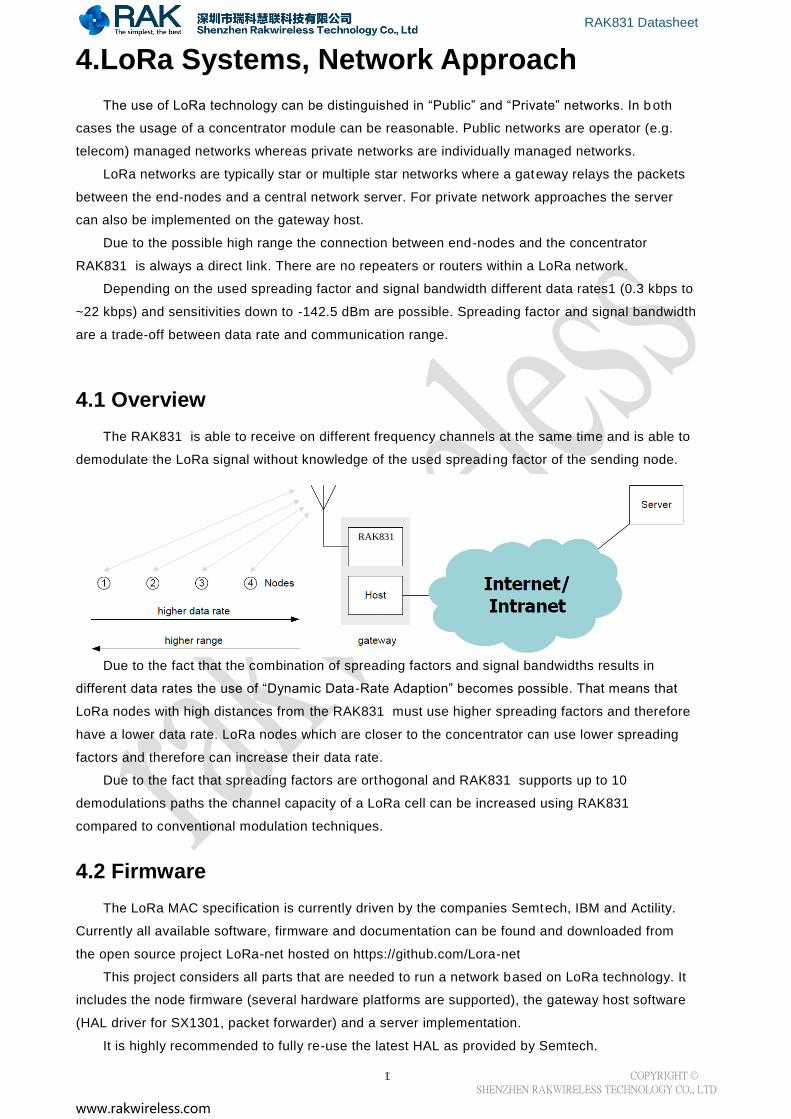
The RAK831 is able to receive on different frequency channels at the same time and is able to
demodulate the LoRa signal without knowledge of the used spreading factor of the sending node.
Due to the fact that the combination of spreading factors and signal bandwidths results in
different data rates the use of “Dynamic Data-Rate Adaption” becomes possible. That means that
LoRa nodes with high distances from the RAK831 must use higher spreading factors and therefore
have a lower data rate. LoRa nodes which are closer to the concentrator can use lower spreading
factors and therefore can increase their data rate.
Due to the fact that spreading factors are orthogonal and RAK831 supports up to 10
demodulations paths the channel capacity of a LoRa cell can be increased using RAK831
compared to conventional modulation techniques.
4.2 Firmware
The LoRa MAC specification is currently driven by the companies Semtech, IBM and Actility.
Currently all available software, firmware and documentation can be found and downloaded from
the open source project LoRa-net hosted on https://github.com/Lora-net
This project considers all parts that are needed to run a network based on LoRa technology. It
includes the node firmware (several hardware platforms are supported), the gateway host software
(HAL driver for SX1301, packet forwarder) and a server implementation.
It is highly recommended to fully re-use the latest HAL as provided by Semtech.
RAK831
RAK831 Datasheet
COPYRIGHT ©
SHENZHEN RAKWIRELESS TECHNOLOGY CO., LTD
www.rakwireless.com
12
5.Electrical Characteristics&Timing specifications
In the following different electrical characteristics of the RAK831 are listed. Furthermore details
and other parameter ranges are available on request.
Note: Stress exceeding of one or more of the limiting values listed under “Absolute Maximum
Ratings” may cause permanent damage to the radio module.
5.1 Absolute Maximum Ratings
Parameter Condition Min Typ. Max Unit
Supply Voltage(VDD) -0.3 5.0 5.5 V
Operating Temperature -40 +85 ℃
RF Iuput Power -15 dBm
Note:
Note: With RF output power level above +15 dBm a minimum distance to a transmitter should be 1 m
for avoiding too large input level.
5.2 Global Electrical Characteristics
Parameter Condition Min Typ. Max Unit
Supply Voltage(VDD) 4.8 5.0 5.2 V
Current Consumption RX Current 100
mA TX Current 80
Note:
T=25℃,VDD=5V(Typ.) if nothing else stated
Parameter Condition Min Typ. Max Unit
Logic low input threshold(VIL) “0”logic input 0.4 V
Logic high input threshold(VIH) “1”logic input 2.9 3.3 V
Logic low output level(VOL) “0”logic output,2mA sink 0.4 V
Logic high output level(VOH) “1”logic output,2mA source 2.9 3.3 V
Note:
RAK831 Datasheet
COPYRIGHT ©
SHENZHEN RAKWIRELESS TECHNOLOGY CO., LTD
www.rakwireless.com
13
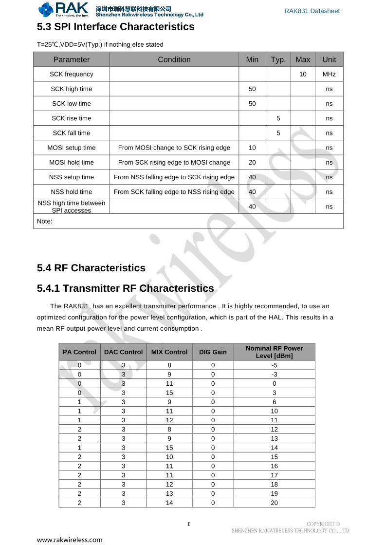
5.3 SPI Interface Characteristics
T=25℃,VDD=5V(Typ.) if nothing else stated
Parameter Condition Min Typ. Max Unit
SCK frequency 10 MHz
SCK high time 50 ns
SCK low time 50 ns
SCK rise time 5 ns
SCK fall time 5 ns
MOSI setup time From MOSI change to SCK rising edge 10 ns
MOSI hold time From SCK rising edge to MOSI change 20 ns
NSS setup time From NSS falling edge to SCK rising edge 40 ns
NSS hold time From SCK falling edge to NSS rising edge 40 ns
NSS high time between SPI accesses
40 ns
Note:
5.4 RF Characteristics
5.4.1 Transmitter RF Characteristics
The RAK831 has an excellent transmitter performance . It is highly recommended, to use an
optimized configuration for the power level configuration, which is part of the HAL. This results in a
mean RF output power level and current consumption .
PA Control DAC Control MIX Control DIG Gain Nominal RF Power
Level [dBm]
0 3 8 0 -5
0 3 9 0 -3
0 3 11 0 0
0 3 15 0 3
1 3 9 0 6
1 3 11 0 10
1 3 12 0 11
2 3 8 0 12
2 3 9 0 13
1 3 15 0 14
2 3 10 0 15
2 3 11 0 16
2 3 11 0 17
2 3 12 0 18
2 3 13 0 19
2 3 14 0 20
RAK831 Datasheet
COPYRIGHT ©
SHENZHEN RAKWIRELESS TECHNOLOGY CO., LTD
www.rakwireless.com
14
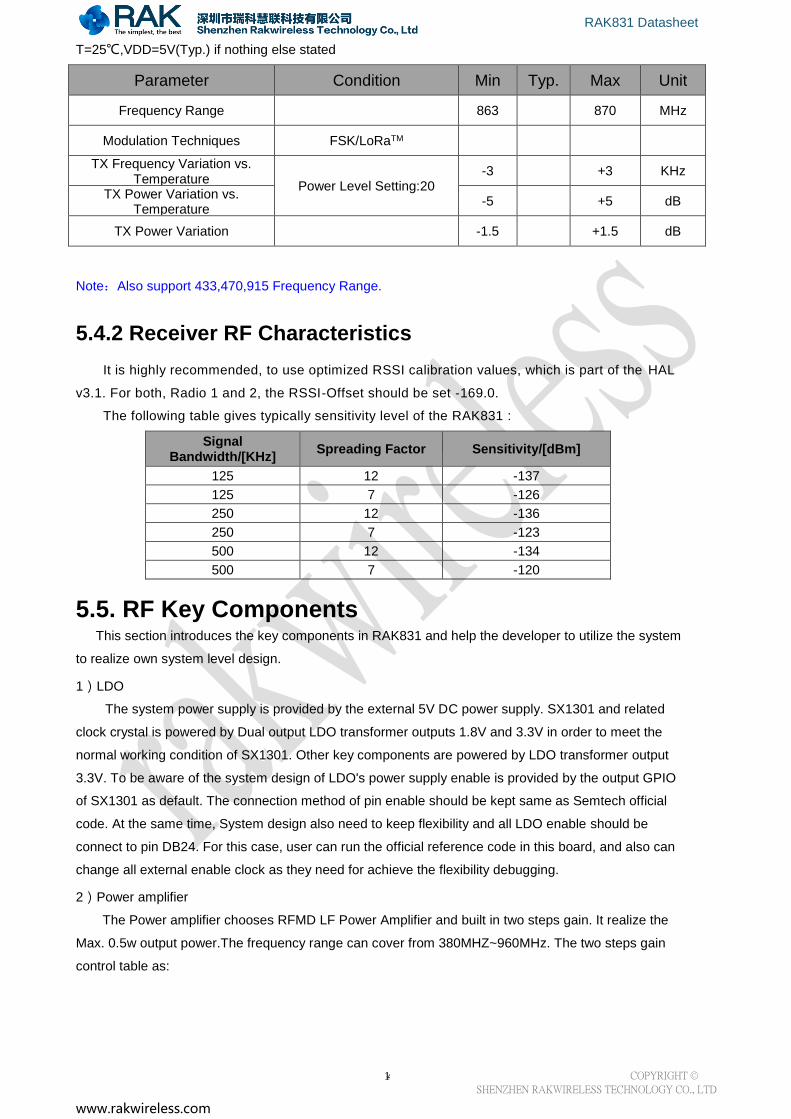
T=25℃,VDD=5V(Typ.) if nothing else stated
Parameter Condition Min Typ. Max Unit
Frequency Range 863 870 MHz
Modulation Techniques FSK/LoRaTM
TX Frequency Variation vs. Temperature
Power Level Setting:20 -3 +3 KHz
TX Power Variation vs. Temperature
-5 +5 dB
TX Power Variation -1.5 +1.5 dB
Note:Also support 433,470,915 Frequency Range.
5.4.2 Receiver RF Characteristics
It is highly recommended, to use optimized RSSI calibration values, which is part of the HAL
v3.1. For both, Radio 1 and 2, the RSSI-Offset should be set -169.0.
The following table gives typically sensitivity level of the RAK831 :
Signal Bandwidth/[KHz]
Spreading Factor Sensitivity/[dBm]
125 12 -137
125 7 -126
250 12 -136
250 7 -123
500 12 -134
500 7 -120
5.5. RF Key Components This section introduces the key components in RAK831 and help the developer to utilize the system
to realize own system level design.
1)LDO
The system power supply is provided by the external 5V DC power supply. SX1301 and related
clock crystal is powered by Dual output LDO transformer outputs 1.8V and 3.3V in order to meet the
normal working condition of SX1301. Other key components are powered by LDO transformer output
3.3V. To be aware of the system design of LDO's power supply enable is provided by the output GPIO
of SX1301 as default. The connection method of pin enable should be kept same as Semtech official
code. At the same time, System design also need to keep flexibility and all LDO enable should be
connect to pin DB24. For this case, user can run the official reference code in this board, and also can
change all external enable clock as they need for achieve the flexibility debugging.
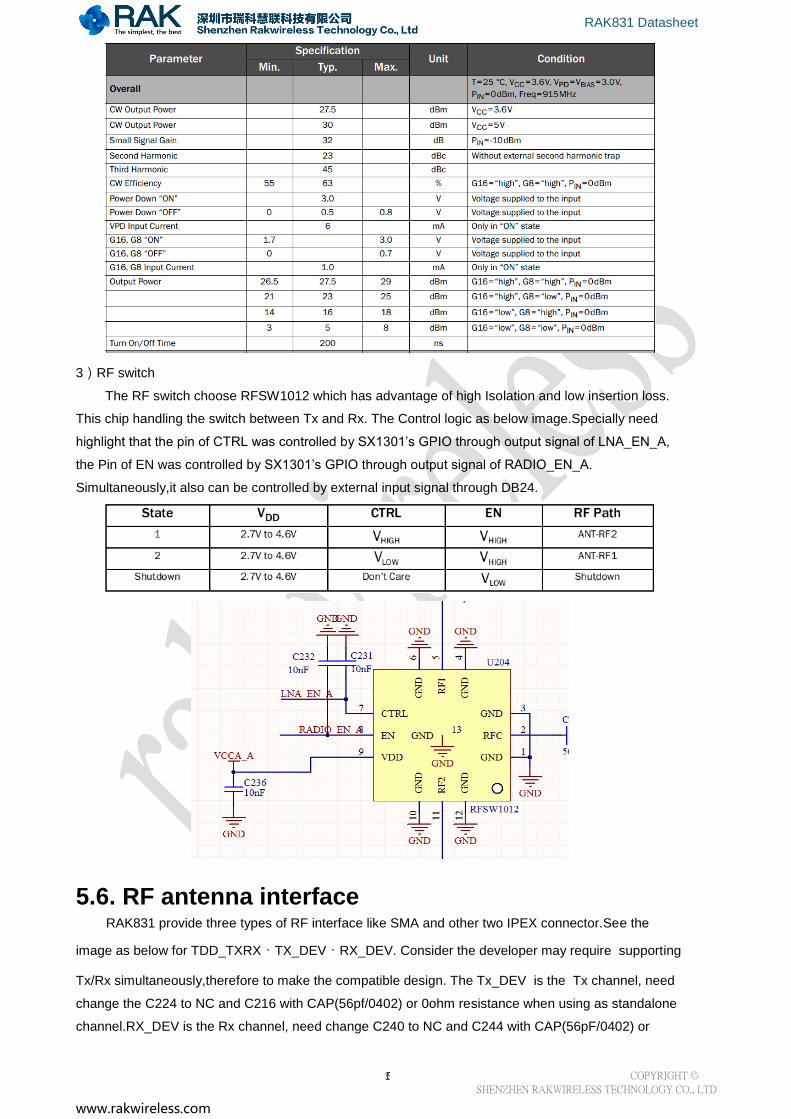
2)Power amplifier
The Power amplifier chooses RFMD LF Power Amplifier and built in two steps gain. It realize the
Max. 0.5w output power.The frequency range can cover from 380MHZ~960MHz. The two steps gain
control table as:
RAK831 Datasheet
COPYRIGHT ©
SHENZHEN RAKWIRELESS TECHNOLOGY CO., LTD
www.rakwireless.com
15
3)RF switch
The RF switch choose RFSW1012 which has advantage of high Isolation and low insertion loss.
This chip handling the switch between Tx and Rx. The Control logic as below image.Specially need
highlight that the pin of CTRL was controlled by SX1301’s GPIO through output signal of LNA_EN_A,
the Pin of EN was controlled by SX1301’s GPIO through output signal of RADIO_EN_A.
Simultaneously,it also can be controlled by external input signal through DB24.
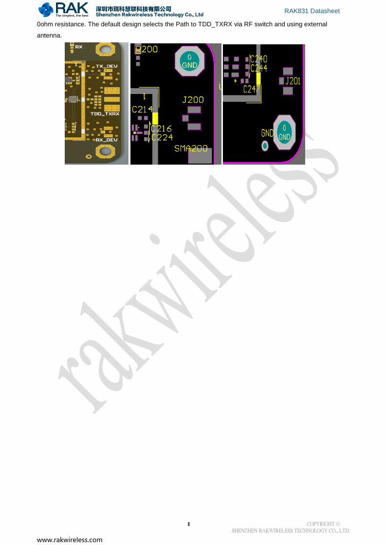
5.6. RF antenna interface RAK831 provide three types of RF interface like SMA and other two IPEX connector.See the
image as below for TDD_TXRX、TX_DEV、RX_DEV. Consider the developer may require supporting
Tx/Rx simultaneously,therefore to make the compatible design. The Tx_DEV is the Tx channel, need
change the C224 to NC and C216 with CAP(56pf/0402) or 0ohm resistance when using as standalone
channel.RX_DEV is the Rx channel, need change C240 to NC and C244 with CAP(56pF/0402) or
RAK831 Datasheet
COPYRIGHT ©
SHENZHEN RAKWIRELESS TECHNOLOGY CO., LTD
www.rakwireless.com
16
0ohm resistance. The default design selects the Path to TDD_TXRX via RF switch and using external
antenna.
RAK831 Datasheet
COPYRIGHT ©
SHENZHEN RAKWIRELESS TECHNOLOGY CO., LTD
www.rakwireless.com
17
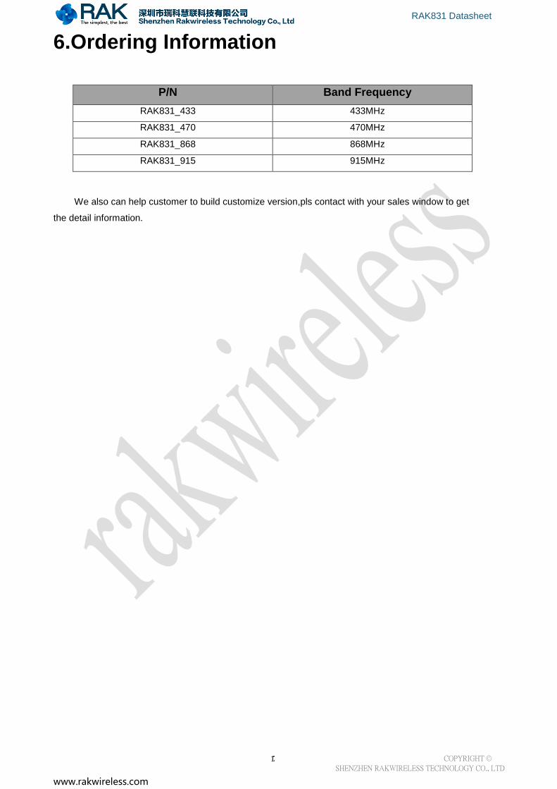
6.Ordering Information
P/N Band Frequency
RAK831_433 433MHz
RAK831_470 470MHz
RAK831_868 868MHz
RAK831_915 915MHz
We also can help customer to build customize version,pls contact with your sales window to get
the detail information.
RAK831 Datasheet
COPYRIGHT ©
SHENZHEN RAKWIRELESS TECHNOLOGY CO., LTD
www.rakwireless.com
18
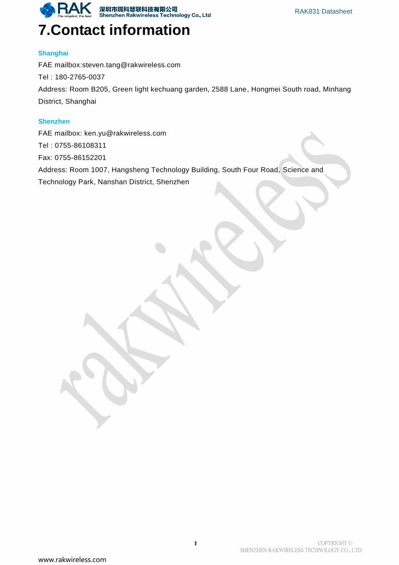
7.Contact information
Shanghai
FAE mailbox:[email protected]
Tel : 180-2765-0037
Address: Room B205, Green light kechuang garden, 2588 Lane, Hongmei South road, Minhang
District, Shanghai
Shenzhen
FAE mailbox: [email protected]
Tel : 0755-86108311
Fax: 0755-86152201
Address: Room 1007, Hangsheng Technology Building, South Four Road, Science and
Technology Park, Nanshan District, Shenzhen
RAK831 Datasheet
COPYRIGHT ©
SHENZHEN RAKWIRELESS TECHNOLOGY CO., LTD
www.rakwireless.com
19
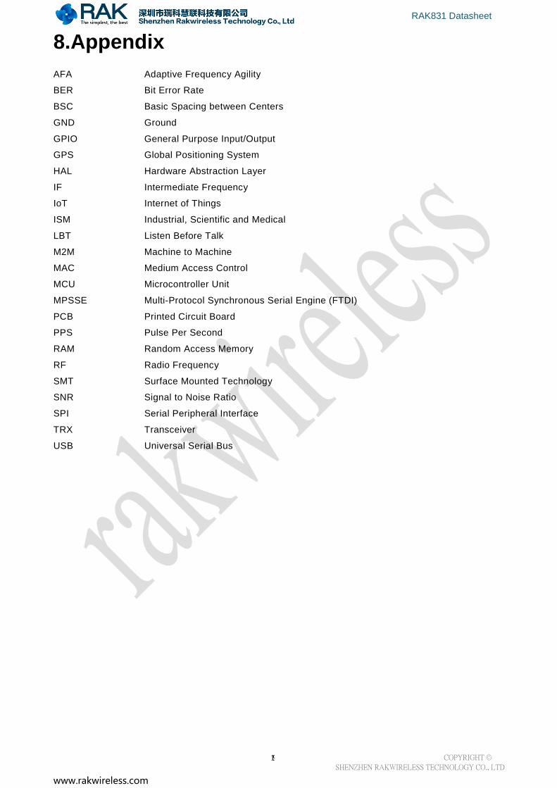
8.Appendix
AFA Adaptive Frequency Agility
BER Bit Error Rate
BSC Basic Spacing between Centers
GND Ground
GPIO General Purpose Input/Output
GPS Global Positioning System
HAL Hardware Abstraction Layer
IF Intermediate Frequency
IoT Internet of Things
ISM Industrial, Scientific and Medical
LBT Listen Before Talk
M2M Machine to Machine
MAC Medium Access Control
MCU Microcontroller Unit
MPSSE Multi-Protocol Synchronous Serial Engine (FTDI)
PCB Printed Circuit Board
PPS Pulse Per Second
RAM Random Access Memory
RF Radio Frequency
SMT Surface Mounted Technology
SNR Signal to Noise Ratio
SPI Serial Peripheral Interface
TRX Transceiver
USB Universal Serial Bus
RAK831 Datasheet
COPYRIGHT ©
SHENZHEN RAKWIRELESS TECHNOLOGY CO., LTD
www.rakwireless.com
20
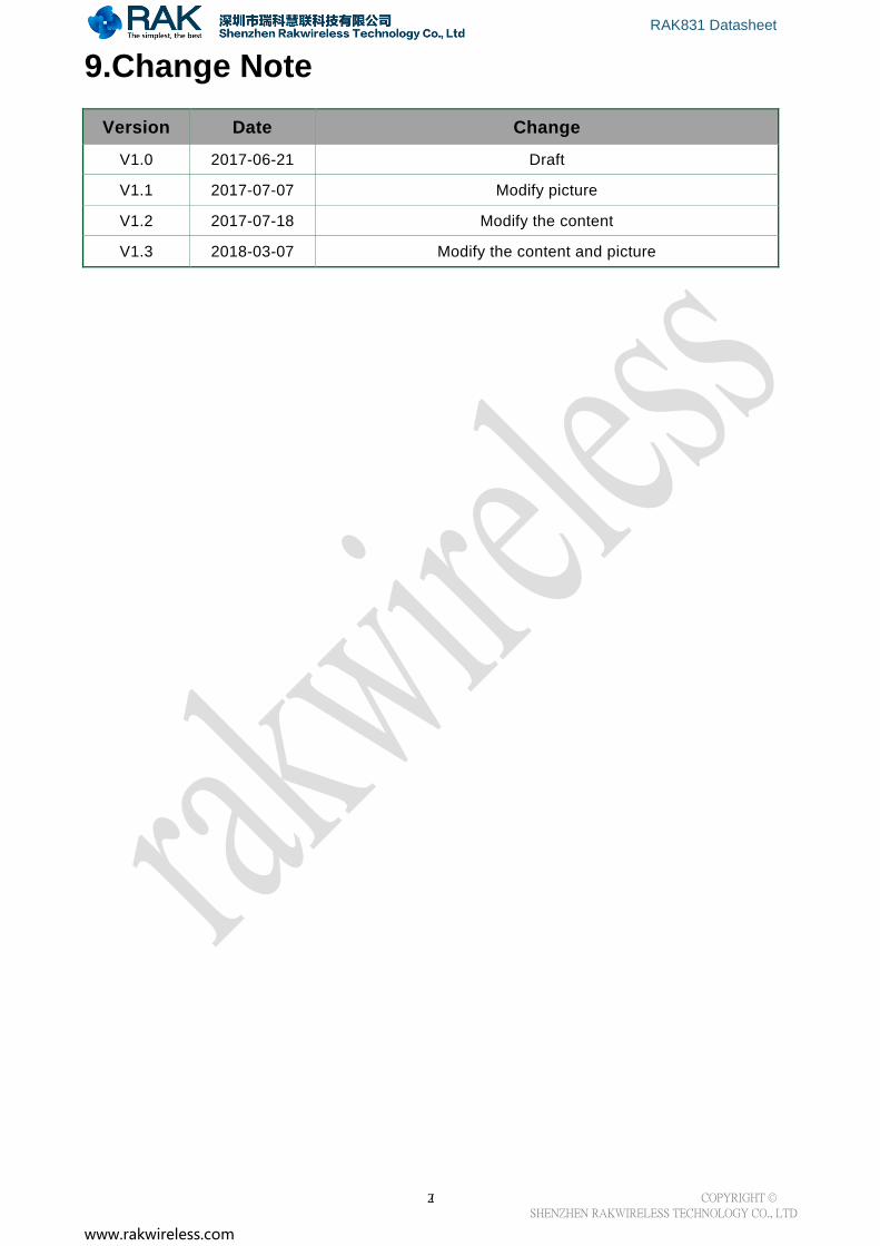
9.Change Note
Version Date Change
V1.0 2017-06-21 Draft
V1.1 2017-07-07 Modify picture
V1.2 2017-07-18 Modify the content
V1.3 2018-03-07 Modify the content and picture