Embed Size (px)
Citation preview
8/3/2019 Rajagopalan Thiruvengadathan et al- Production and Characterization of Silicon Nanostructures for the Advanceme…
http://slidepdf.com/reader/full/rajagopalan-thiruvengadathan-et-al-production-and-characterization-of-silicon 1/7
1
PRODUCTION AND CHARACTERIZATION OF SILICON NANOSTRUCTURES FOR THE
ADVANCEMENT OF NOVEL ENERGETIC FORMULATIONS
Rajagopalan Thiruvengadathan, Andrey Bezmelnitsyn, Maxim Shub, Steven Apperson,
Keshab Gangopadhyay and Shubhra Gangopadhyay*
Department of Electrical and Computer Engineering,
University of Missouri, Columbia, MO 65211 (USA)
Paul Anderson and Wendy Balas
US Army ARDEC, Picatinny Arsenal, NJ 07806(USA)
ABSTRACT
This paper details the synthesis and characterization of
Silicon (Si) nanostructured powder with a wide variety of
morphologies such as nanoparticles, nanowires,
nanotubes etc produced by DC plasma arc discharge
route. These nanostructures were synthesized bycontrolling the synthesis parameters such as current,
voltage, catalyst, gas pressure etc. The structural,
morphological and vibrational properties were
investigated using X-ray diffraction, transmission electron
microscopy, scanning electron microscopy, nitrogen
adsorption-desorption isotherms and Raman
Spectrometer. Both bright and dark field imaging were
performed in order to study the morphological
characteristics of the nanostructures. These images
confirm the formation of high aspect ratio nanostructures
of Si with diameters of up to 15 nm and lengths in the
range of 500 – 1000 nm. Diffraction patterns were
recorded to identify the number of phases formed anddetermine the crystal structure of the observed phases.
The BET surface area of Si nanoparticles and high aspect
ratio Si nanostructures (nanowires and nanotubes) are
about 60 m2 /g and 360 m2 /g respectively. Raman
spectrum of nanostructured Si showed both shift in the
peak position and broadening of the Raman peak.
1. INTRODUCTION
In recent years, there is a renewed interest on the
development of nanostructured silicon (Si) to advance the
preparation of next generation energetic formulations.
Two significant achievements that spurred this interest
were the demonstration of (i) the preparation of a
explosive composite based on porous Si filled with
gadolinium nitrate (Gd(NO3)3) in 2002. [Mikulec et al,
2002] and (ii) explosive reaction of nanoporous silicon
immersed in cryogenic oxygen discovered in 2001.
[Kovalev et al, 2001]. The growing interest in porous
silicon is attributed to its high reactivity with oxygen
owing to high internal surface area and higher energy of
the exothermic reaction of silicon and oxygen than that of
the most common carbon-based explosives. [Clément et
al, 2005] Therefore, it is envisaged that the energetic
compositions based on silicon will be extremely useful in
several applications including in microarray analysis, as a
smart ignition system for conventional explosives or as a
propulsion system for microelectromechanical systems(MEMS) Moreover the energetic mixture prepared with
silicon nanostructures is thermally more stable because of
its higher melting point as compared to Al. The energetic
formulation based on nano Si is also relatively more ESD
insensitive.
These scientific developments motivated us to
produce silicon nanostructured powder in our laboratory.
In this paper, we report the preparation and
characterization of silicon nanostructured powder using
DC arc-discharge system, in particular, with an emphasis
on the production of high aspect ratio Si nanostructures
such as nanowires and nanotubes. Silicon nanotubes and
nanowires with large surface area and high mechanicalstrength are likely to be a better choice of fuel compared
to porous silicon and silicon nanoparticles. In this work,
iron was used as a metal catalyst to prepare nanowires and
nanotubes.
2. EXPERIMENTAL
2.1 Materials
Silicon wafers were crushed into powders and used
as a precursor in the synthesis process. Iron powder with
particle size less than <10 μm and purity of 99.9+ %
obtained from Sigma Aldrich (product number: 267953)
was used as the catalyst.
2.2 Synthesis of Si Nanostructured Powder
An attempt to grow high aspect ratio Si
nanomaterials is described below. This was accomplished
through the use of the plasma arc discharge reactor
similar to those used for fullerene and nanotube synthesis.
8/3/2019 Rajagopalan Thiruvengadathan et al- Production and Characterization of Silicon Nanostructures for the Advanceme…
http://slidepdf.com/reader/full/rajagopalan-thiruvengadathan-et-al-production-and-characterization-of-silicon 2/7
Report Documentation PageForm Approved
OMB No. 0704-0188
Public reporting burden for the collection of information is estimated to average 1 hour per response, including the time for reviewing instructions, searching existing data sources, gathering and
maintaining the data needed, and completing and reviewing the collection of information. Send comments regarding this burden estimate or any other aspect of this collection of information,
including suggestions for reducing this burden, to Washington Headquarters Services, Directorate for Information Operations and Reports, 1215 Jefferson Davis Highway, Suite 1204, Arlington
VA 22202-4302. Respondents should be aware that notwithstanding any other provision of law, no person shall be subject to a penalty for failing t o comply with a collection of information if it
does not display a currently valid OMB control number.
1. REPORT DATE
DEC 2008
2. REPORT TYPE
N/A
3. DATES COVERED
-
4. TITLE AND SUBTITLE
Production And Characterization Of Silicon Nanostructures For The
Advancement Of Novel Energetic Formulations
5a. CONTRACT NUMBER
5b. GRANT NUMBER
5c. PROGRAM ELEMENT NUMBER
6. AUTHOR(S) 5d. PROJECT NUMBER
5e. TASK NUMBER
5f. WORK UNIT NUMBER
7. PERFORMING ORGANIZATION NAME(S) AND ADDRESS(ES)
Department of Electrical and Computer Engineering, University of
Missouri, Columbia, MO 65211 (USA)
8. PERFORMING ORGANIZATION
REPORT NUMBER
9. SPONSORING/MONITORING AGENCY NAME(S) AND ADDRESS(ES) 10. SPONSOR/MONITOR’S ACRONYM(S)
11. SPONSOR/MONITOR’S REPORT
NUMBER(S)
12. DISTRIBUTION/AVAILABILITY STATEMENT
Approved for public release, distribution unlimited
13. SUPPLEMENTARY NOTES
See also ADM002187. Proceedings of the Army Science Conference (26th) Held in Orlando, Florida on 1-4
December 2008, The original document contains color images.
14. ABSTRACT
15. SUBJECT TERMS
16. SECURITY CLASSIFICATION OF: 17. LIMITATION OF
ABSTRACT
UU
18. NUMBER
OF PAGES
6
19a. NAME OF
RESPONSIBLE PERSON a. REPORT
unclassified
b. ABSTRACT
unclassified
c. THIS PAGE
unclassified
Standard Form 298 (Rev. 8-98)
Prescribed by ANSI Std Z39-18
8/3/2019 Rajagopalan Thiruvengadathan et al- Production and Characterization of Silicon Nanostructures for the Advanceme…
http://slidepdf.com/reader/full/rajagopalan-thiruvengadathan-et-al-production-and-characterization-of-silicon 3/7
2
A graphite cup 3” in diameter and 7/8” in height wasfilled with a feedstock consisting of crushed silicon waferand iron powder acting as catalyst for the growth of highaspect ratio Si nanostructures. Typically, three partscrushed silicon powder mixed with one part iron powderwere used as the precursor in the arc-reactor. In some of the experiments, crushed Si powder was used without ironpowder to understand the role of iron in the synthesis of Si nanostructures. The cathode was a ¼” diameter puretungsten electrode. The reactor chamber was water-cooledduring the entire duration of discharge.
The typical parameters used in the reactor operationwere in the range of 25 – 75 A of current, 20-30 V and ata pressure of 40-100 kPa of Argon. These parameterswere varied in an attempt to optimize the synthesisprocess for realizing high aspect ratio Si nanostructures.
2.3 Preparation of Energetic Mixtures
Accurately weighed 0.2 g of CuO nanorods and Sinanopowder were mixed together at an equivalence ratioof 1.6 in 2-propanol. The mixture was sonicated in anultrasonic bath (Fisher 8835) for 6-8 hrs. The slurry wasdried at 95oC for 15 min to obtain powder.
2.4 Material Characterization
A variety of analytical tools were employed toinvestigate the fundamental structural, morphological andvibrational characteristics of the obtained Sinanostructured powder. X-ray diffraction and electrondiffraction experiments were performed to determine the
crystalline nature of the sample and indirect estimation of the chemical composition through the determination of lattice parameters. A Ultima IV Rigaku X-raydiffractometer was used in X-ray difftactionmeasurements. Both bright and dark field imaging wasperformed using a high resolution transmission electronmicroscope (Model: JEOL JEM 2000FX operated at 200kV and Philips (FEI) EM420T (Tungsten Emitter)operated at 120 kV. X-ray Energy-DispersiveSpectroscopy (EDS) was also simultaneously performedto determine the composition. A scanning electronmicroscope (SEM) (Model: Hitachi S-4700) was alsoused to determine the morphological characteristics of the
sample.Nitrogen adsorption–desorption isotherms were
measured using a Quantachrome Autosorb-1 automatedgas sorption system and the surface areas were computedusing the Brunauer–Emmett–Teller (BET) method.Raman measurements were performed using RenishawinVia spectrometer system equipped with Hg Arc Lampillumination with 360nm excitation and >400nmcollection and an Argon Ion laser (20mW) excitation, at514nm.
2.5 Reactivity Measurements
Reactivity measurements were performed bymeasuring the pressure generated as a function of timeduring the combustion propagation. Typically, a sampleof 20mg powder was loaded in a cylindrical metal well(diameter – 6.25 mm and depth – 2mm) for each test. Ni-alloy fuse wire with a diameter of 0.13mm was used forthe ignition of nanothermite material and this wire was indirect contact with the nanothermite.
Piezoelectric based pressure sensor (PCBPiezotronics Model 119B12, fastened to a rigid steelholder. was mounted directly on the top of the milli-wellpre-loaded with the nanothermite material. The entiresystem was secured together by a rigid clamp and thusreducing the pressure leakage to the maximum extent.The thermite material was ignited by step applying DCvoltage by SCR controlled capacitor discharge firing
block. After blowing fuse wire the combustion processwas recorded by pressure sensor. Pressure measurementerror with this calibration procedure is within ± 10%.
The ESD sensitivity tests of these samples wereperformed using a measurement system fabricated byElectro-Tech Systems (ETS) Inc. Typically 2 - 4 mgnanopowdered thermite was placed in the sample holder.The sample is charged and discharged at 5000 V withvarying capacitance values to obtain different energiesand the number of charging/discharging cycles used in thepresent measurement is 24. A sample is considered ESDpass if it did not ignite upon charging. This means that
the sample passes at all ESD energies equal or below thevalues.
3. RESULTS AND DISCUSSION
The synthesis process of Si nanostructures, thereactor was closely monitored during the synthesisprocess to adjust the distance between the cathode and theanode. Fumes were observed coming out of the graphitecup, indicating the evaporation of Si charge. Dependingon the DC arc operation parameters used, the color of theresultant product varied. When a high current above 75Awas used in the synthesis, the obtained powder was more
blackish in color. This sample is found to contain carbonand copper impurities owing to the partial melting of theelectrode assembly. When a current of 40-50 A was usedin the synthesis, the color of the obtained powder wasdark greenish with a slight yellowish shade. If ironpowder was not used, the resultant color is moreyellowish. Different colors of the obtained Sinanostructures indicated that it could be related to thecomposition and the various morphologies formed.Therefore, it is necessary to optimize the synthesisparameters to realize tunable nanostructured powder with
8/3/2019 Rajagopalan Thiruvengadathan et al- Production and Characterization of Silicon Nanostructures for the Advanceme…
http://slidepdf.com/reader/full/rajagopalan-thiruvengadathan-et-al-production-and-characterization-of-silicon 4/7
3
a specific morphology. It was observed that with an arccurrent of 40-50 A, sheets of material could be peeled off
from the walls of the reactor indicating the formation of
fibrous material. Visual observation of individual piecesof this material shows a relatively high strength.
3.1 Crystal Structure
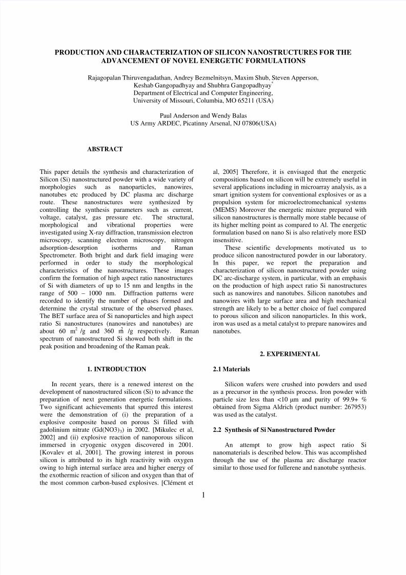
Figure 1 shows a typical wide angle X-raydiffractogram obtained for Si nanostructured powderproduced with parameters, I = 50 A, voltage = 25 V and1:3 weight ratios of iron to Si powder in Ar ambient. It isevident that the sample is predominantly crystalline innature. The observed peak positions were compared withthose of powder diffraction files maintained by JointCommittee on Powder Diffraction Standards (JCPDS).
The X-ray diffraction measurement revealed that thesample consists of essentially two crystalline phases – (a)Si and (b) FeSi2. The crystal structure of Si phase is cubicdiamond with a lattice constant of 5.43 Å while that of FeSi2 is tetragonal with a = b = 2.69 Å and c= 5.14 Å.This finding was confirmed from electron diffractionpattern also as will be shown in the next section. The
broadened diffraction peaks indicate the reduceddimensions of the Si nanopowder formed with DC arc-discharge.
3.2 Morphological Characteristics
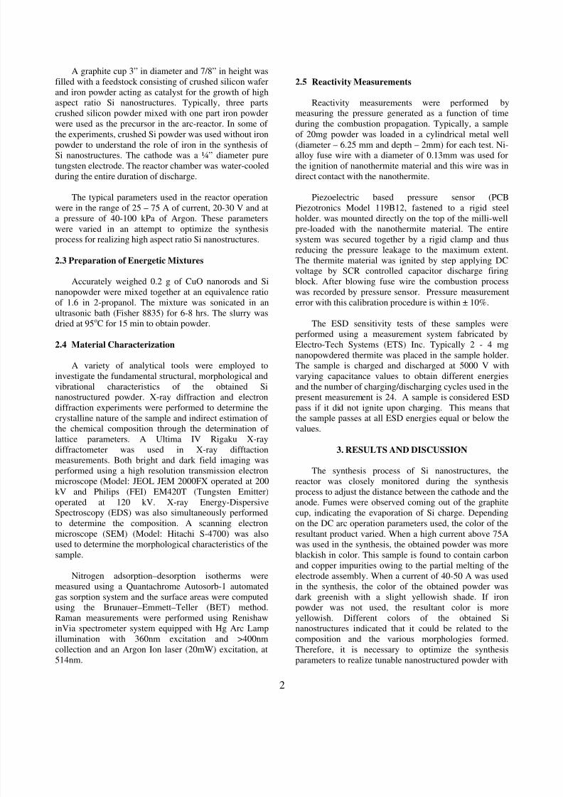
Detailed imaging of the obtained Si nanostructuredpowder facilitated their morphological properties such astheir shape and dimensions. The typical image recordedfor Si nanopowder formed with arc reactor parameters of 25A and 30V without using iron as catalyst shown inFigure 2 reveals that the morphology of the Sinanopowder is spherical nanoparticles with a sizedistribution in the range of 5- 40 nm.
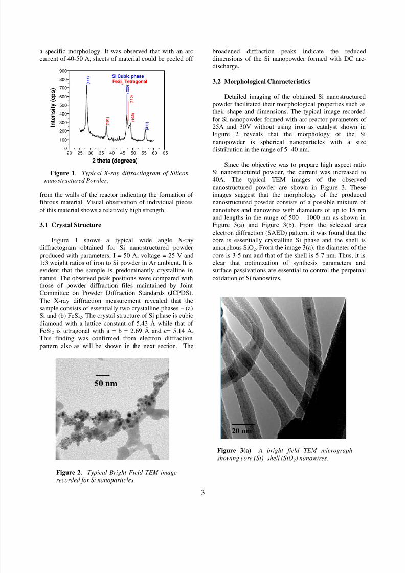
Since the objective was to prepare high aspect ratioSi nanostructured powder, the current was increased to40A. The typical TEM images of the observednanostructured powder are shown in Figure 3. Theseimages suggest that the morphology of the produced
nanostructured powder consists of a possible mixture of nanotubes and nanowires with diameters of up to 15 nmand lengths in the range of 500 – 1000 nm as shown inFigure 3(a) and Figure 3(b). From the selected areaelectron diffraction (SAED) pattern, it was found that thecore is essentially crystalline Si phase and the shell isamorphous SiO2. From the image 3(a), the diameter of thecore is 3-5 nm and that of the shell is 5-7 nm. Thus, it isclear that optimization of synthesis parameters andsurface passivations are essential to control the perpetualoxidation of Si nanowires.
20 nm
Figure 3(a) A bright field TEM micrograph
showing core (Si)- shell (SiO2) nanowires.
50 nm
Figure 2. Typical Bright Field TEM image
recorded for Si nanoparticles.
20 25 30 35 40 45 50 55 60 650
100
200
300
400
500
600
700
800
900
FeSi2
TetragonalSi Cubic phase
( 3 1 1 ) ( 1
0 2 )
( 1 1 0 )
( 2 2 0 )
( 1 0 1 )
I n t e n s i t y ( c p s )
2 theta (degrees)
( 1 1 1 )
Figure 1. Typical X-ray diffractiogram of Silicon
nanostructured Powder .
8/3/2019 Rajagopalan Thiruvengadathan et al- Production and Characterization of Silicon Nanostructures for the Advanceme…
http://slidepdf.com/reader/full/rajagopalan-thiruvengadathan-et-al-production-and-characterization-of-silicon 5/7
4
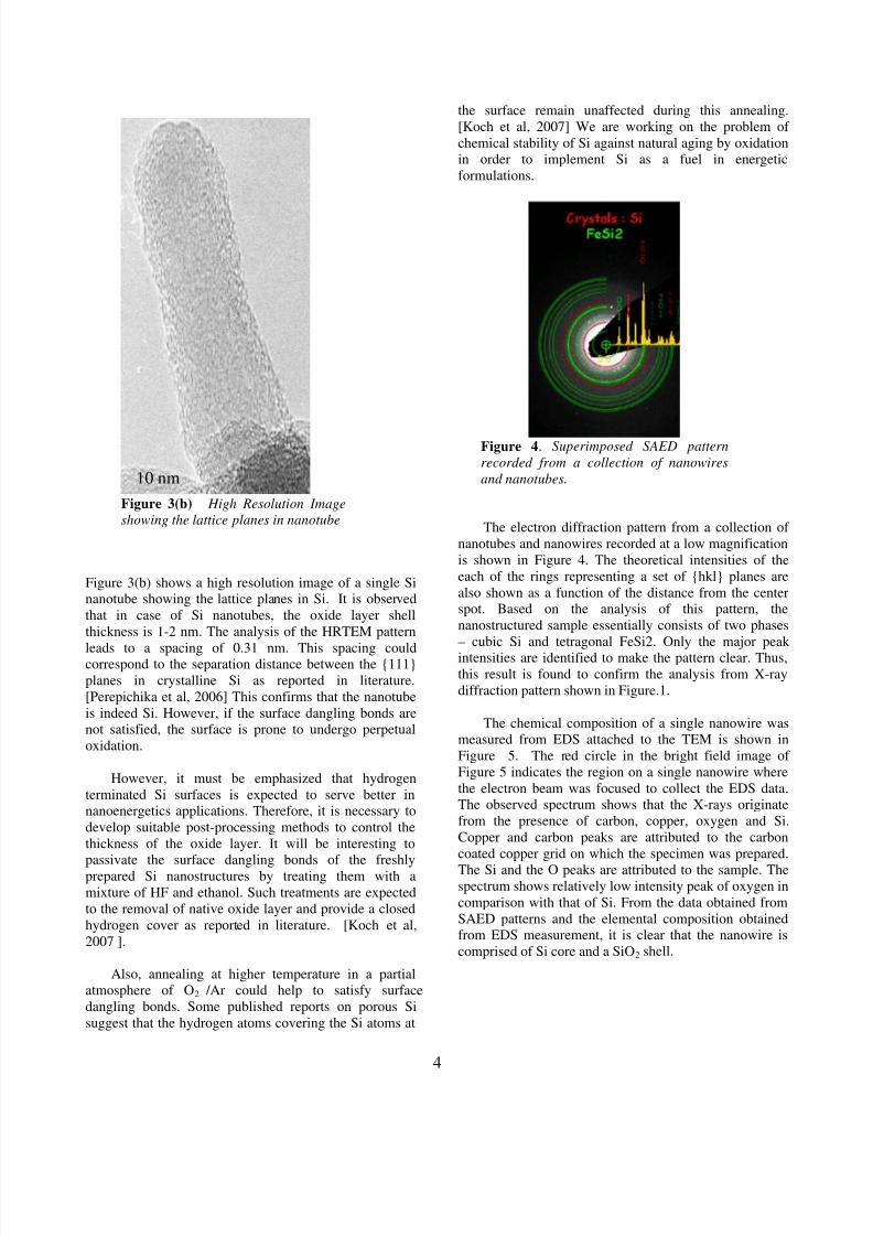
Figure 3(b) shows a high resolution image of a single Sinanotube showing the lattice planes in Si. It is observedthat in case of Si nanotubes, the oxide layer shellthickness is 1-2 nm. The analysis of the HRTEM pattern
leads to a spacing of 0.31 nm. This spacing couldcorrespond to the separation distance between the {111}planes in crystalline Si as reported in literature.[Perepichika et al, 2006] This confirms that the nanotubeis indeed Si. However, if the surface dangling bonds arenot satisfied, the surface is prone to undergo perpetualoxidation.
However, it must be emphasized that hydrogenterminated Si surfaces is expected to serve better innanoenergetics applications. Therefore, it is necessary todevelop suitable post-processing methods to control thethickness of the oxide layer. It will be interesting to
passivate the surface dangling bonds of the freshlyprepared Si nanostructures by treating them with amixture of HF and ethanol. Such treatments are expectedto the removal of native oxide layer and provide a closedhydrogen cover as reported in literature. [Koch et al,2007 ].
Also, annealing at higher temperature in a partialatmosphere of O2 /Ar could help to satisfy surfacedangling bonds. Some published reports on porous Sisuggest that the hydrogen atoms covering the Si atoms at
the surface remain unaffected during this annealing.[Koch et al, 2007] We are working on the problem of chemical stability of Si against natural aging by oxidationin order to implement Si as a fuel in energeticformulations.
The electron diffraction pattern from a collection of nanotubes and nanowires recorded at a low magnificationis shown in Figure 4. The theoretical intensities of theeach of the rings representing a set of {hkl} planes arealso shown as a function of the distance from the centerspot. Based on the analysis of this pattern, thenanostructured sample essentially consists of two phases– cubic Si and tetragonal FeSi2. Only the major peakintensities are identified to make the pattern clear. Thus,this result is found to confirm the analysis from X-raydiffraction pattern shown in Figure.1.
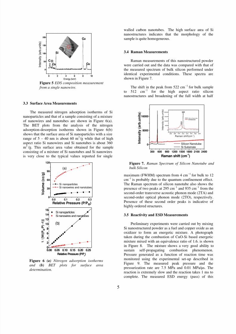
The chemical composition of a single nanowire wasmeasured from EDS attached to the TEM is shown inFigure 5. The red circle in the bright field image of Figure 5 indicates the region on a single nanowire wherethe electron beam was focused to collect the EDS data.The observed spectrum shows that the X-rays originatefrom the presence of carbon, copper, oxygen and Si.Copper and carbon peaks are attributed to the carboncoated copper grid on which the specimen was prepared.
The Si and the O peaks are attributed to the sample. Thespectrum shows relatively low intensity peak of oxygen incomparison with that of Si. From the data obtained fromSAED patterns and the elemental composition obtainedfrom EDS measurement, it is clear that the nanowire iscomprised of Si core and a SiO2 shell.
Figure 3(b) High Resolution Image
showing the lattice planes in nanotube
10 nm
Figure 4. Superimposed SAED pattern
recorded from a collection of nanowires
and nanotubes.
8/3/2019 Rajagopalan Thiruvengadathan et al- Production and Characterization of Silicon Nanostructures for the Advanceme…
http://slidepdf.com/reader/full/rajagopalan-thiruvengadathan-et-al-production-and-characterization-of-silicon 6/7
5
3.3 Surface Area Measurements
The measured nitrogen adsorption isotherms of Si
nanoparticles and that of a sample consisting of a mixtureof nanowires and nanotubes are shown in Figure 6(a).The BET plots from the analysis of the nitrogenadsorption-desorption isotherms shown in Figure 6(b)shows that the surface area of Si nanoparticles with a sizerange of 5 – 40 nm is about 60 m2 /g while that of highaspect ratio Si nanowires and Si nanotubes is about 360m2 /g. This surface area value obtained for the sampleconsisting of a mixture of Si nanotubes and Si nanowiresis very close to the typical values reported for single
walled carbon nanotubes. The high surface area of Sinanostructures indicates that the morphology of thesample is quite homogeneous.
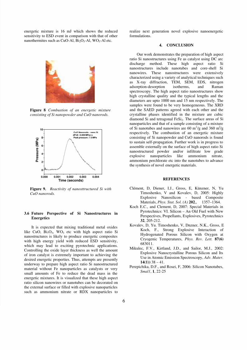
3.4 Raman Measurements
Raman measurements of this nanostructured powderwere carried out and the data was compared with that of the measured spectrum of bulk silicon performed underidentical experimental conditions. These spectra areshown in Figure 7.
The shift in the peak from 522 cm−1 for bulk sampleto 512 cm−1 for the high aspect ratio siliconnanostructures and broadening of the full width at half
maximum (FWHM) spectrum from 4 cm−1
for bulk to 12cm−1 is probably due to the quantum confinement effect.The Raman spectrum of silicon nanotube also shows thepresence of two peaks at 295 cm−1 and 935 cm−1 from thesecond-order transverse acoustic phonon mode (2TA) andsecond-order optical phonon mode (2TO), respectively.Presence of these second order peaks is indicative of highly ordered structures.
3.5 Reactivity and ESD Measurements
Preliminary experiments were carried out by mixingSi nanostructured powder as a fuel and copper oxide as an
oxidizer to form an energetic mixture. A photographtaken during the combustion of CuO-Si based energeticmixture mixed with an equivalence ratio of 1.6. is shownin Figure 8. The mixture shows a very good ability tosustain self-propagating combustion phenomenon.Pressure generated as a function of reaction time wasmonitored using the experimental set-up described inFigure 9. The measured peak pressure and thepressurization rate are 7.5 MPa and 0.01 MPa/µs. Thereaction is extremely slow and the reaction takes 1 ms tocomplete. The measured ESD energy (pass) of this
0 2 4 6 8 10
0
50
100
150
200
Si
Cu
Cu
CuO
I n t e n s i t y
( a r b . u n i t s )
Energy (keV)
C
Figure 5 EDS composition measurement
from a single nanowire.
0.0 0.1 0.2 0.30
30
60
90
120
Si nanoparticlesSi nanowires and nanotubes
Relative Pressure (P/Po)
V o l u m e ( c c / g )
(a)
0.00 0.05 0.10 0.15 0.20 0.250
2
46
8
10
12
14
16
(b)
Si nanoparticles
Si nanowires and nanotubes
1 / [ W ( ( P o
/ P ) - 1 ) ]
Relative Pressure (P/Po)
Figure 6 (a) Nitrogen adsorption isotherms
and (b) BET plots for surface area
determination.
300 600 900 1200 1500 1800 2100 2400
0
8000
16000
460 480 500 520 540 560 580 600
0
5000
10000
15000
20000 522
5 1 2
Silicon Nanotube Si Substrate
I n t e n s i t y
( a r b
. u n i t s )
Raman shift(cm-1
)
Silicon Nanotube
Si Substrate
I n t e n s i t y ( a r b . u n
i t s )
Raman shift (cm-1)
Figure 7. Raman Spectrum of Silicon Nanotube and
bulk Silicon
8/3/2019 Rajagopalan Thiruvengadathan et al- Production and Characterization of Silicon Nanostructures for the Advanceme…
http://slidepdf.com/reader/full/rajagopalan-thiruvengadathan-et-al-production-and-characterization-of-silicon 7/7
6
energetic mixture is 16 mJ which shows the reducedsensitivity to ESD event in comparison with that of othernanothermites such as CuO-Al, Bi2O3-Al, WO3-Al etc.
3.6 Future Perspective of Si Nanostructures in
Energetics
It is expected that mixing traditional metal oxideslike CuO, Bi2O3, WO3 etc with high aspect ratio Sinanostructures is likely to produce energetic compositeswith high energy yield with reduced ESD sensitivity,
which may lead to exciting pyrotechnic applications.Controlling the oxide layer thickness as well the amountof iron catalyst is extremely important to achieving thedesired energetic properties. Thus, attempts are presentlyunderway to prepare high aspect ratio Si nanostructuredmaterial without Fe nanoparticles as catalysts or verysmall amounts of Fe to reduce the dead mass in theenergetic mixtures. It is visualized that these high aspectratio silicon nanowires or nanotubes can be decorated onthe external surface or filled with explosive nanoparticlessuch as ammonium nitrate or RDX nanoparticles to
realize next generation novel explosive nanoenergeticformulations.
4. CONCLUSION
Our work demonstrates the preparation of high aspectratio Si nanostructures using Fe as catalyst using DC arcdischarge method. These high aspect ratio Sinanostructures include nanotubes and core-shell Sinanowires. These nanostructures were extensivelycharacterized using a variety of analytical techniques suchas X-ray diffraction, TEM, SEM, EDS, nitrogenadsorption-desorption isotherms, and Ramanspectroscopy. The high aspect ratio nanostructures showhigh crystalline quality and the typical lengths and thediameters are upto 1000 nm and 15 nm respectively. Thesamples were found to be very homogeneous. The XRDand the SAED patterns agreed with each other and thecrystalline phases identified in the mixture are cubicdiamond Si and tetragonal FeSi2. The surface areas of Si
nanoparticles and that of a sample consisting of a mixtureof Si nanotubes and nanowires are 60 m2 /g and 360 m2 /grespectively. The combustion of an energetic mixtureconsisting of Si nanopowder and CuO nanorods is foundto sustain self-propagation. Further work is in progress toassemble externally on the surface of high aspect ratio Sinanostructured powder and/or infiltrate low gradeexplosive nanoparticles like ammonium nitrate,ammonium perchlorate etc into the nanotubes to advancethe synthesis of novel energetic materials.
REFERENCES
Clément, D, Diener, I.J., Gross, E, Künzner, N, YuTimoshenko, V and Kovalev, D, 2005: HighlyExplosive Nanosilicon - based CompositeMaterials, Phys. Stat. Sol. (A) 202,, 1357–1364.
Koch E.C., and Clement, D, 2007: Special Materials inPyrotechnics: VI. Silicon – An Old Fuel with NewPerspectives, Propellants, Explosives, Pyrotechnics32, 205-212.
Kovalev, D, Yu. Timoshenko, V, Dnzner, N.K., Gross, EKoch, F., Strong Explosive Interaction of Hydrogenated Porous Silicon with Oxygen atCryogenic Temperatures, Phys. Rev. Lett. 87(6)
683011.Mikulec, F.V., Kirtland, J.D., and Sailor, M.J., 2002:Explosive Nanocrystalline Porous Silicon and ItsUse in Atomic Emission Spectroscopy, Adv. Mater. 14(1)) 38 – 41.
Perepichika, D.F., and Rosei, F, 2006: Silicon Nanotubes,Smal1, 1, 22-25
Figure 8 Combustion of an energetic mixture
consisting of Si nanopowder and CuO nanorods.
0.000 0.001 0.002 0.003 0.004
0
2
4
6
8
10
P r e s s u r e ( M P a )
Time (seconds)
CuO Nanorods - nano Si
dP/dt : 0.009 MPa/μs
Peak pressure : 7.5 MPa
Figure 9. Reactivity of nanosttructured Si with
CuO nanorods.