Embed Size (px)
Citation preview

Advances in Radio Science, 3, 75–81, 2005SRef-ID: 1684-9973/ars/2005-3-75© Copernicus GmbH 2005
Advances inRadio Science
A Fractional Ramp Generator with Improved Linearity andPhase-Noise Performance for the Use in Heterodyne MeasurementSystems
T. Musch and B. Schiek
Institut fur Hochfrequenztechnik, Ruhr-Universitat Bochum, Universitatsstraße 150, 44780 Bochum, Germany
Abstract. Concepts for the generation and the measurementof highly linear frequency ramps are presented. The frac-tional ramp synthesiser concept shown here is able to gener-ate frequency ramps with a very low phase noise level, a verygood frequency linearity and reproducibility.
Related to the bandwidth of the generated frequency rampsof 4.5 GHz a relative linearity error below 4·10−10 is demon-strated in a prototype system. This linearity error is close tothe limit set by the phase noise floor of the ramp generatorsand marks a significant improvement over existing aproaches(Musch and Schiek, 2000). The basic measurement sensitiv-ity due to the phase noise is 1.8·10−10 without averaging.
As the phase noise is important for the linearity of the fre-quency ramp the set-up has to be optimised for a good phasenoise behaviour, too. In order to achieve this good phasenoise a special phase-frequency detector is introduced that isespecially designed for the use in a fractional phase lockedloop.
1 Introduction
The generation of extremely linear frequency ramps is im-portant in high precision applications like heterodyne mea-surement systems. Industrial measurement systems oftenrely on fast, precise and additionally cost effective measure-ments. Highly linear frequency ramps offer the possibilityof achieving those requirements altogether. One outstandingexample of a measurement system with the highest demandsfor high precision frequency synthesis are accurate hetero-dyne vector network analysers (VNA).
Conventional vector network analysers are based onstepped frequency synthesisers which are quite easy to im-plement because static frequencies with a small frequencydifference are simple to generate using standard phase-locked-loop (PLL) concepts. Since stepped frequency syn-thesisers are comparably slow when a high number of
Correspondence to:T. Musch([email protected])
discrete frequencies is necessary, fast measurement systemsbenefit from analogue frequency ramps.
These dynamic frequency ramps are able to run quicklyover a wide frequency band while at the same time they offera high density of frequency samples. This is due to the factthat a ramp based system does not need the settling times ofstepped frequency systems. In the VNA the analogue fre-quency ramps allow both for high speed measurements witha large number of frequencies being measured and a good ac-curacy on the condition that the frequency ramp generationis very stable.
Even more than absolute linearity errors of the frequencyramps, non-reproducible frequency ramps have detrimentaleffects on the measurement results in a VNA. Therefore agood reproducibility of the frequency ramps is the most im-portant requirement of the ramp synthesisers besides a highramp linearity. A reproducibility of the ramp frequency inthe range of a few Hz is feasible. The fractional divider tech-nique offers new solutions for highly linear, precise and ro-bust ramp generators.
Key components(Schiek, 1999) of such fractional fre-quency ramp synthesisers are the division factor generationin the fractional frequency divider as well as the phase-frequency detector (PFD). The division factor generation is acompletely digital part. Nevertheless the implemented algo-rithm generating the division factor sequence has a great in-fluence on the overall phase noise performance of the wholesystem. A low division factor deviation(Musch and Schiek,2001) is essential to reduce the noise-floor of the phase-frequency detector in the fractional mode of operation.
The PFD is a mixed digital/analogue component that di-rectly and largely influences the phase noise behaviour of thesynthesiser. This PFD has to operate extremely linearly, as itis very sensitive to the down-conversion of the unavoidablehigh-frequency fractional noise to non-filterable frequenciesclose to the carrier.
Finally, together with some compensation schemes, theramp linearity is only limited by the phase noise level of thefractional PLL as stated below. This is the reason for theefforts made to reduce the phase noise level.

76 T. Musch and B. Schiek: A Fractional Ramp Generator
✻4
R
V
R
V
✲
✲fref
fv
+−
+−
✲✲
✲✲
✲
✲❄❄
✲
✲
LP
LP +PD
FD
F (s)
✲
✲ ✲
✲
✲
✲
LD1
LD2
fv > fr
fv < fr
✲ ✲Utune
low noisepower-supply
pulse-shaper
✗
✕
Fig. 1. Block diagram of the linear PFD with separated phase- andfrequency detector.
2 A highly linear phase-frequency detector
Besides the broadband voltage controlled oscillator and thecrystal reference oscillator, the key components in a frac-tional PLL are the fractional divider and the PFD.
The most important properties of the PFD are the linearityof the output voltage versus the input phase difference andthe noise floor in the non-fractional mode of operation. Thephase noise floor in the non-fractional mode marks the lowerbound of the achievable phase noise in the fractional mode.The reason for this is the fact that the non-fractional phasenoise is stochastically independent of the down-convertedfractional noise, thus adding to the spectral power of the frac-tional noise.
The phase noise in the non-fractional mode of opera-tion is mainly caused by analogue noise phenomena in thePFD-circuit while the fractional noise arises from the quasi-stochastic changes of the division factors of the fractionaldivider. In the strict sense the fractional noise is a determin-istic phenomenon but since the periodicity is extremely long,in the range of several hours, it can be treated as a stochasticsignal.
To achieve a low non-fractional phase noise behaviour itis important to use only low noise components in the criticalsignal path and to keep the critical signal path as simple aspossible. In order to realise this, a separation of the phasedetecting part responsible for the phase noise properties andthe frequency detecting part only used during the pull-in pro-cess is applied in the PFD. The principle block diagram ofthe phase-frequency detector with the separation approachis shown in Fig.1. The phase detector (PD) comprises twoD-type flip-flops while the frequency detector (FD) is muchmore complex. The reference clock inputs R are fed by thepulse shaped signals from the reference oscillator e.g. a crys-tal controlled oscillator. The VCO-inputs V on the other aretriggered by the output signals from the fractional dividerwhich is located between the VCO and the PFD. The phasedetector has a gain of
Kpd =4 V
2π(1)
including the first mixed digital/analogue stage.The frequency detector does not affect the gain of the
phase detector. It consists of two blocks. One block is for thedetection of large frequency differences to enable a fast lock
Fig. 2. Photography of the linear PFD with separated phase- andfrequency detector.
process. The other block is a four-quadrant phase-follower.Both blocks are combined in the frequency detector (FD)block in Fig. 1 with the two lock detect outputs LD1 andLD2 indicating if the divided VCO-frequencyfv is higher orlower than the reference frequencyfref . If the PLL is lockedthan both lock detect outputs are low.
In case that the phase is outside of the allowed range, thefrequency detector intervenes upon the phase detector andforces the VCO in the desired direction. This is done bymeans of the control lines between the frequency detectorand the phase detector. The control lines are not active whenthe PLL is locked so that no interferences and spurious sig-nals are injected into the sensitive parts of the phase detec-tor. As the frequency detector is quite complex and does notaffect the phase noise, it is implemented in a complex pro-grammable logic device (CPLD).
This separation enables the phase noise sensitive phase de-tector to be kept simple. Furthermore the phase detector partcan be operated under optimal bias conditions regarding thephase difference thus exhibiting a very good linearity.
Besides this optimal phase bias a first highly linear mixeddigital/analogue stage is necessary. To achieve the highestpossible performance this part of the circuit is built with dis-crete components in a balanced structure. The balancing isused to suppress unwanted intermodulation products. Fig-ure2 shows a photography of the PFD circuit. The loop filter(F(s)) of the fractional PLL is also located on this circuitboard to avoid crosstalk with other circuit parts. The loop fil-ter contains the important low-pass filter that suppresses thehigher noise frequencies of the fractional divider. Since thefractional divider produces strongly noisy signals at higherfrequencies by nature, the low-pass filter is essential to blockthese fractional noise components from reaching the VCO.
The transfer function of the low-pass filter versus fre-quency has to be of a higher order than the shaped digital

T. Musch and B. Schiek: A Fractional Ramp Generator 77
Fig. 3. Photography of the fractional divider circuit with the FPGAincluding the input and output components.
noise of the fractional logic thus suppressing the fractionalnoise even in the region of its steepest rise. As the fractionallogic is of fourth order the overall low-pass characteristic ofthe loop filter is of fifth order.
A fundamental factor of the PLL is the theoretically lowestpossible phase noise level that occurs in the non-fractionalmode of operation. This phase noise floorW c
φ,pd of the PFDrelated to the carrier is below
W cφ,pd = −152 dBc/Hz @ 5 kHz (2)
with a reference frequency at the PFD of 50 MHz. The PFDdesign is optimised for high comparison frequencies up to100 MHz. But as the time jitter of the PFD above 50 MHz isnearly constant, an increase of the reference frequency above50 MHz results in a decreasing phase noise level at the PFD.This decreasing phase noise level at the PFD has the effectthat a higher reference frequency together with a lower di-vision ratio in the frequency divider does not improve thephase noise level at the VCO significantly. The effect of thedecreasing division factor is partly compensated by the risingphase noise level at the PFD.
3 A low noise fractional ramp division factor generator
Besides the PFD the fractional divider is of great impor-tance for the noise performance of the fractional PLL andfor the overall ramp linearity. Especially the division factorsequences are of great concern as they strongly influence thephase noise of the PLL.
In the prototype system the programmable microwave fre-quency divider together with the controller for the divider,which is implemented in a field programmable gate array(FPGA), as well as the complete input and display unit arelocated on one printed circuit board. Figure3 depicts aphotography of this fractional divider board. The FPGA is
I IFIR
z−1
+ +
✻ ✻
✲ ✲ ✲ ✲ ✲ ✲✲FNf
− −+❄
P
✲II
K2K1
++
✻✻
✻✻
✲✲ ✲✲−− z−1
❄
N
nq
❄✲ ✲
Fig. 4. Simplified block diagram of the four-stage fractional logiccore with an additional delay element in the integrator chain.
surrounded by the input and display unit, the high frequencyprogrammable divider, the flash memory, the serial EPROMand finally a low noise power supply. The FPGA generatesthe fractional division factors and contains the ramp genera-tor as well as most parts of the input and display unit.
For the ramp generation several different methods are im-plemented. One is the internal linear ramp generation witha counter based ramp unit. This block is able to produceexactly linear frequency ramps without any additional fre-quency modulation on the ramp. If an additional frequencymodulation is desired, another ramp mode based on a flashmemory is used. This ramp mode allows for nearly arbitraryramp shapes because the ramp curve is completely stored in-side the memory.
As the flash memory is not able to handle clock frequen-cies in the range of 50 MHz or even more, an undersamplingapproach is chosen with a memory clock rate of a fourth ofthe fractional logic clock frequency. An additional interpo-lation stage calculates the missing interim values resultingin a smooth and highly accurate frequency curve. Besidesthe reduction of the memory clock rate the undersamplingapproach also reduces the memory space that is required tostore one complete frequency ramp.
Since the division factorsN of the programmable fre-quency divider are quite low in the range of
8 ≤ N ≤ 28 (3)
the fractional logic should not have a high division factor de-viation 1N around the average fractional division factorN .A large deviation1N would cause a high down-convertedfractional noise. As a consequence, a simple sigma deltaconcept with cascaded integrator stages (, Racal, 1978,R)will not work properly. Therefore, a special fractional logicstructure is used that generates fractional division factor se-quences with a reduced deviation1N .
Additionally, the concept includes a pipelining structurethat allows very high clock frequencies of the fractional logiccore of more than 100 MHz. In practice, the maximum clockrate of the fractional logic is not the limiting factor for thereference frequency because the division factors would be-come too low with higher reference frequencies.
Average division factors below 12 are dangerous with re-spect to the down-conversion of the fractional noise. Thisis in fact the major limitation. Nevertheless, concerning thephase noise, it would not make much sense to move to higherreference frequencies because the time jitter of the PFD isnearly constant above 50 MHz.

78 T. Musch and B. Schiek: A Fractional Ramp Generator
N
0 200 400 600 800 100018
19
20
21
22
n
Fig. 5. Calculated part of a division factor sequence generated bythe four-stage fractional logic.
The main idea behind the pipelining concept is to imple-ment multiple delay stages in the fractional logic core. Asimplified block diagram of a four-stage fractional core withtwo delay elements is shown in Fig.4. The circuit behaviouris described using the z-Transform. The integratorsI withthe transfer function
I (z) =1
1 − z−1(4)
in the forward path are producing the noise shaping effect,which suppresses the fractional noisenq close to the carrier.
The fractional noisenq is caused by the quantisation at theoutput of the chain. The coefficientsK1 andK2 have twoessential tasks. Firstly, with the help of these coefficientsthe division factor deviation is reduced. Secondly, the co-efficients are necessary to ensure a stable operation of thefractional logic.
A minimum of one delay elementz−1 is necessary for afeasible digital feedback loop. By using one more delay ele-ment in the main signal path of the fractional core it is possi-ble to synchronise the digital data stream inside the logic tothe clock signal.
This is because of the additional delay element whichbreaks up the long chain of adders and integrators thus allow-ing for higher clock frequencies by roughly a factor of two.The FIR-filter in the input of the fractional logic compen-sates for the transfer function of the fractional logic exceptfor a residual delay, which does not affect the performanceof the fractional PLL.
Without the FIR-filter the transfer function of the frac-tional modulator chain in the z-domain can be derived fromthe block diagram in Fig.4 as
Nf (z) =F(z)z−1
+ nq(z)D4(z)
V (z)(5)
where the denominatorV (z) is defined as
V (z) = D3(z)K2 + D2(z)(1 − 2K2 + K1)
+D(z)(K2 − 2K1) + K1. (6)
Ref Lvl
15 dBm
1VIEW
-30
-20
-10
0
10
15
Delta 1 [T1 NOI]
-106.93 dBc/Hz
5.00000000 kHz
FXD 12.255 dBm
Fig. 6. Measurement of the phase noise level of the fractional PLLin the static mode.
The time discrete transfer function of the differentiatorD(z)
is given by
D(z) = 1 − z−1. (7)
A stability analysis is necessary to ensure a stable operationof the fractional logic. The two coefficients in the feedbackpath of the fractional logic are chosen to be
K1 = 3/16, (8)
K2 = 1/2. (9)
With these coefficients the system is working in the stableregion. Besides the stability an important factor of the frac-tional logic is the amplitude of the division factor variationthat is necessary to produce the mean fractional division ra-tios.
This division factor deviation strongly influences thedown-conversion of the high-pass shaped fractional noise inthe PFD. With the coefficientsK1 andK2 the reduced peakto peak division factor deviation1N results in
1N = 4. (10)
This means that with an average division ratioN=20.05 thedivision factors at the output of the fractional logic vary in arange between 18≤N≤22. By way of a simulation an exem-plary section of such a division factor sequence is shown inFig. 5.
The division factors are shown versus the numbern ofclock cycles.
4 Measurements based on a dual fractional PLL rampsystem
In order to verify the performance of the fractional PLL con-cept two categories of measurements are made with two pro-totype PLL circuits.

T. Musch and B. Schiek: A Fractional Ramp Generator 79
∼
÷N1 PFD1
F1(s)✛ ✛
✲ ✛
∼
✻❄
✲ ✲
XCO
÷8✲
❄
❄
VCO1
fa,1
❄
✲
∼
÷N2PFD2
F2(s) ✲✲
✛
✻❄
✛✛ ÷8 ✛
❄
❄
VCO2
fa,2
fref
fractionalmasterlogic
fractionalslavelogic
CLK CLK
✲Sync
❄fi.f.
Fig. 7. Block diagram of the dual ramp system.
Firstly, to check the phase noise performance of the sys-tem a measurement with one of the two fractional PLLs isarranged in the static mode with a fixed frequency of roughly8 GHz. A low phase noise spectrum analyser is used to di-rectly record the spectrum close to the carrier from which thephase noise can be read. The result of this measurement isshown in Fig.6. The phase noise level at an offset frequencyof 5 kHz is in the order of−107 dBc/Hz. This is a very goodresult for a single loop fractional PLL with a VCO outputfrequency of 8 GHz.
The same measurement with the PLL in the non-fractionalmode at an output frequency of exactly 8 GHz results ina phase noise level of−108 dBc/Hz at a 5 kHz offset fre-quency. This demonstrates the good linearity of the PFDbecause there is only 1 dB difference between the non-fractional mode, showing the minimum phase noise floorof the PLL, and the fractional mode that adds additionalfractional noise, which is down-converted due to the non-linearity of the PFD characteristic.
The good phase noise behaviour is relying on both a highlylinear PFD and additionally a fractional logic offering a lowdivision factor deviation. Together with a high reference fre-quency a good ramp linearity is feasible, which is finally lim-ited by the phase noise of the PLLs.
From the phase noise level at the output of the VCO it ispossible to calculate the equivalent phase noise level at thePFD operating at 50 MHz. The phase noise level at the PFDreferred to the carrier results in
W cφ,pd(5 kHz) =
W cφ,vco(5 kHz)
N2
= −108 dBc/Hz− 10 log(N2)
= −152 dBc/Hz. (11)
This phase noise level comprises the phase noise influencesof the divider and the crystal oscillator, too. Therefore, thenoise floor of the PFD is well below−152 dBc/Hz.
To measure the ramp linearity a dual loop set-up is used.The dual loop approach allows for highly sensitive measure-ments with a frequency resolution of some hundred mHz.The idea is to run two extremely linear frequency ramps inparallel and down-convert the difference frequency to an i.f.-signal. The frequencies of the i.f.-signal are in the range of
∆f
Hz
0 5 10 15 20 25 30 35 40 45 50-15
-10
-5
0
5
10
15
t/ms
Fig. 8. Measured frequency deviation between the two parallel fre-quency ramps.
some kHz and can easily be sampled in an analogue to digitalconverter (ADC).
The block diagram of the dual loop system is depicted inFig. 7.
At the output of the mixer the i.f.-signal is present at a lowintermediate frequency of
fi.f. = |fa,2 − fa,1| ≈ 3 kHz. (12)
After a low pass filtering of the i.f.-signal to keep the mi-crowave frequencies of the ramps away from the next signalprocessing stages, the i.f.-signal is sampled in an analogue todigital converter. Then, the data can be processed in a com-puter.
For a highly sensitive signal processing the spectrum of thei.f.-signal is calculated first by means of a Fourier transform.Within the i.f.-spectrum a certain bandwidth around the i.f.spectral peak is filtered. This bandwidth has to be chosenproperly in order to include all relevant spectral sidebandscarrying information about the non-linearity. If, on the otherhand, the bandwidth is wider than necessary the noise on thei.f.-signal reduces the sensitivity of the measurement. Thefilter bandwidth in the following measurements is chosen as2 kHz.
The spectrum at negative frequencies is set to zero and thecomplex analytical time signal is calculated via an inverseFourier Transform. The derivative of the angle of this com-plex analytical time signal is equal to the frequency deviationbetween the two frequency ramps. To ensure the relevanceof the linearity measurement an unwanted synchronicity be-tween the two ramps has to be avoided.
To ensure this the measurement set-up comprises for ex-ample different VCOs and different fractional divider se-quences thus suppressing ganging effects. Figure8 showsthe result of such a linearity measurement with the two VCOsrunning from 4.5 GHz up to 9 GHz with a ramp bandwidth of
Br = 4.5 GHz (13)

80 T. Musch and B. Schiek: A Fractional Ramp Generator
∆f
Hz
0 50-2
-1.5
-1
-0.5
0
0.5
1
1.5
2
5 10 15 20 25 30 35 40 45t/ms
Fig. 9. Measured frequency deviation between the two frequencyramps using the frequency error compensation.
and a ramp time of
Tr = 50 ms (14)
having a difference frequencyfi.f. of roughly 3 kHz. Themaximum frequency error is in the order of±13 Hz. Re-lated to the bandwidth this results in a relative non-linearityof 2.9·10−9.
With the realistic assumption that both fractional rampPLLs show uncorrelated frequency deviations from the idealramp with approximately the same magnitude, the non-linearity of each ramp generator results as 1/
√2 times the
deviation measured in Fig.8. The estimated non-linearity ofeach ramp is in the order of 2.1·10−9. This is already a verygood ramp linearity.
In order to illustrate the potential of the fractional rampconcept the measured frequency error in Fig.8 can be usedto frequency modulate one of the fractional ramp PLLs withthe inverse frequency error to compensate for it. After thiscompensation a new linearity measurement is carried out andthe result is shown in Fig.9. The frequency error after imple-menting the compensation is in the range of±1.5 Hz. Thusthe relative non-linearity is better than 3.4·10−10.
A further interesting question concerns the sensitivity ofthe measurement and the influence of the phase noise. There-fore the same non-linearity evaluation can be performedwhen both PLLs are working in the static mode having fixedfrequencies and a fixed difference frequency because no lin-earity error can influence the measurement result in this case.The only factor to be taken into consideration is the phasenoise.
With the result from the phase noise measurement in Fig.6it is possible to estimate the frequency error with the mea-surement method described above.
The first step is to calculate the phase noise of thei.f.-signal. The mixing of two signals with uncorrelatednoise contributions increases the phase noise level by 3 dBcompared to the phase noise of each individual oscillator.
Furthermore, the i.f.-frequency is much smaller than the loopbandwidth of the PLL of roughly 400 kHz.
The two frequencies at the mixer are so close to eachother that the uncorrelated phase noise from both sidebandsis down-converted to the i.f.-signal thus further reducing thephase noise level by 3 dB. From this the expected phase noiselevel of the i.f.-signal is
W cφ,i.f.(5 kHz) = −107 dBc/Hz+ 6 dB
= −101 dBc/Hz. (15)
With some additional noise from the ADC and the i.f.-amplifier the overall i.f.-phase noise level could be slightlyhigher.
For the further calculations the knowledge of the shape ofthe i.f.-phase noise spectrum is necessary. As a PLL showsa white spectrum well below the cut-off frequency of theclosed loop it is quite easy to describe the shape of the i.f.-spectrum. Including the flicker noise corner frequencyωc thei.f.-phase noise spectrum can be described as
W cφ,i.f.(ωof ) =
∣∣∣∣1 +ωc
ωof
∣∣∣∣ · W cφ,i.f.(5 kHz). (16)
The value of interest that can be compared with the resultsof the linearity measurements in Figs.8 and9 is the varianceof the i.f.-frequency as calculated from the analytical timesignal within the filter bandwidth of 2 kHz.
To derive this value the energy of the frequency noisewithin the filter bandwidth of 2 kHz has to be evaluated.Therefore, at first the frequency spectrum is calculated fromthe phase noise spectrum in Eq. (16) to be
W cω,i.f.(ωof ) =
∣∣∣∣1 +ωc
ωof
∣∣∣∣·ω2of ·W c
φ,i.f.(5 kHz). (17)
From this frequency noise spectrum the varianceσ 2ω,i.f. of
the i.f.-frequency results from an integration over the filterbandwidth as
σ 2ω,i.f. =
1
2π
ωg∫−ωg
∣∣∣∣1 +ωc
ωof
∣∣∣∣·W c
φ,i.f.(5 kHz) · ω2of · dωof
=1
πW c
φ,i.f.(5 kHz)
(ω3
g
3+ ωc
ω2g
2
). (18)
With the varianceσ 2ω,i.f. the standard deviationσf,i.f. of the
i.f.-frequency in Hz can be calculated directly resulting in
σf,i.f. =1
2πσω,i.f.
=1
2π
√√√√ 1
πW c
φ,i.f.(5 kHz)
(ω3
g
3+ ωc
ω2g
2
). (19)
With the value of−101 dBc/Hz for the i.f.-phase noiselevel at 5 kHz offset frequency, a cut-off frequency
T. Musch and B. Schiek: A Fractional Ramp Generator 81
∆f
Hz
0 5 10 15 20 25 30 35 40 45 50-0.8
-0.6
-0.4
-0.2
0
0.2
0.4
0.6
0.8
1
t/ms
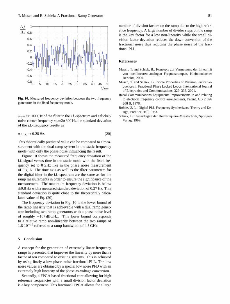
Fig. 10. Measured frequency deviation between the two frequencygenerators in the fixed frequency mode.
ωg=2π1000 Hz of the filter in the i.f.-spectrum and a flicker-noise corner frequencyωc=2π300 Hz the standard deviationof the i.f.-frequency results as
σf,i.f. ≈ 0.28 Hz. (20)
This theoretically predicted value can be compared to a mea-surement with the dual ramp system in the static frequencymode, with only the phase noise influencing the result.
Figure10 shows the measured frequency deviation of thei.f.-signal versus time in the static mode with the fixed fre-quency set to 8 GHz like in the phase noise measurementof Fig. 6. The time axis as well as the filter parameters forthe digital filter in the i.f.-spectrum are the same as for theramp measurements in order to ensure the significance of themeasurement. The maximum frequency deviation is below±0.8 Hz with a measured standard deviation of 0.27 Hz. Thisstandard deviation is quite close to the theoretically calcu-lated value of Eq. (20).
The frequency deviation in Fig.10 is the lower bound ofthe ramp linearity that is achievable with a dual ramp gener-ator including two ramp generators with a phase noise levelof roughly −107 dBc/Hz. This lower bound correspondsto a relative ramp non-linearity between the two ramps of1.8·10−10 referred to a ramp-bandwidth of 4.5 GHz.
5 Conclusion
A concept for the generation of extremely linear frequencyramps is presented that improves the linearity by more than afactor of ten compared to existing systems. This is achievedby using firstly a low phase noise fractional PLL. The lownoise values are obtained by a special low noise PFD with anextremely high linearity of the phase-to-voltage conversion.
Secondly, a FPGA based fractional core allowing for highreference frequencies with a small division factor deviationis a key component. This fractional FPGA allows for a large
number of division factors on the ramp due to the high refer-ence frequency. A large number of divider steps on the rampis the key factor for a low non-linearity while the small di-vision factor deviation reduces the down-conversion of thefractional noise thus reducing the phase noise of the frac-tional PLL.
References
Musch, T. and Schiek, B.: Konzepte zur Vermessung der Linearitatvon hochlinearen analogen Frequenzrampen, KleinheubacherBerichte, 2000.
Musch, T. and Schiek, B.: Some Properties of Division Factor Se-quences in Fractional Phase Locked Loops, International Journalof Electronics and Communications, 329–336, 2001.
Racal Communications Equipment: Improvements in and relatingto electrical frequency control arrangements, Patent, GB 2 026268 B, 1978.
Rohde, U. L.: Digital PLL Frequency Synthesizers, Theory and De-sign, Prentice Hall, 1983.
Schiek, B.: Grundlagen der Hochfrequenz-Messtechnik, Springer-Verlag, 1999.


![Fractional Cascading Fractional Cascading I: A Data Structuring Technique Fractional Cascading II: Applications [Chazaelle & Guibas 1986] Dynamic Fractional](https://img.pdfslide.us/doc/110x75/56649ea25503460f94ba64dd/fractional-cascading-fractional-cascading-i-a-data-structuring-technique-fractional.jpg)