Embed Size (px)
Citation preview
DDF1 • 1
DOPPLER DIRECTION FINDER
RADIO DIRECTION FINDER KIT
Ramsey Electronics Model No. DDF1
Get in on the fun of radio direction finding (RDF) with this super kit ! The latest in affordable Doppler direction finding equipment available in a complete kit form ..this one even includes the receiving antenna. A must for the “fox hunter” at an unheard of price!
• Elegant and cost effective design thanks to WA2EBY ! Featured in May / June 1999 QST Articles.
• Solid state antenna switching for “rock solid” performance.
• Convenient LED 22.5 degree bearing indicator.
• Audio Level indicator for trouble free operation.
• Adjustable damping rate, phase inversion, scan enable / disable.
• Complete with home brew “mag mount” antennas and cable, designed for quick set up and operation.
• Utilizes latest high speed CMOS technology for signal conditioning and audio processing!
• Complete and informative instructions guide you to a kit that works the first time, every time - enhances resale value, too !

DDF1 • 2
RAMSEY TRANSMITTER KITS • The “Cube” MicroStation Transmitter • FM25B Synthesized FM Stereo Transmitter • FM100B “Professional Quality” Stereo FM Transmitter • AM1, AM25 AM Transmitters RAMSEY RECEIVER KITS • FR1 FM Broadcast Receiver • AR1 Aircraft Band Receiver • SR1 Shortwave Receiver • AA7 Active Antenna • SC1 Shortwave Converter RAMSEY HOBBY KITS • SG7 Personal Speed Radar • SS70A Speech Scrambler • MX Series High Performance Mixer • MD3 Microwave Motion Detector • PICPRO Pic Chip Programmer • LC1 Inductance-Capacitance Meter RAMSEY AMATEUR RADIO KITS • DDF1 Doppler Direction Finder • HR Series HF All Mode Receivers • QRP Series HF CW Transmitters • CW7 CW Keyer • CPO3 Code Practice Oscillator • QRP Power Amplifiers RAMSEY MINI-KITS Many other kits are available for hobby, school, Scouts and just plain FUN. New kits are always under development. Write or call for our free Ramsey catalog.
DDF1 DOPPLER RADIO DIRECTION FINDER KIT INSTRUCTION MANUAL
Ramsey Electronics publication No. MDDF1 Revision 1.2 First printing: May, 1999
COPYRIGHT 1998 by Ramsey Electronics, Inc. 590 Fishers Station Drive, Victor, New York 14564. All rights reserved. No portion of this publication may be copied or duplicated without the written permission of Ramsey Electronics, Inc. Printed in the United States of America.
DDF1 • 3
DOPPLER RADIO DIRECTION FINDER
Ramsey Publication No. MDDF1 Price $5.00
TABLE OF CONTENTS Introduction to the DDF1 ............... 4 DDF1 Circuit Description .............. 4 Parts List ...................................... 11 DDF1 Assembly Steps ................. 14 Component Layout ....................... 17 Schematic Diagram ...................... 18 Initial Testing ................................ 22 Ramsey Warranty ........................ 23
INSTRUCTION MANUAL FOR
RAMSEY ELECTRONICS, INC. 590 Fishers Station Drive
Victor, New York 14564 Phone (585) 924-4560
Fax (585) 924-4555 www.ramseykits.com
DDF1 • 4
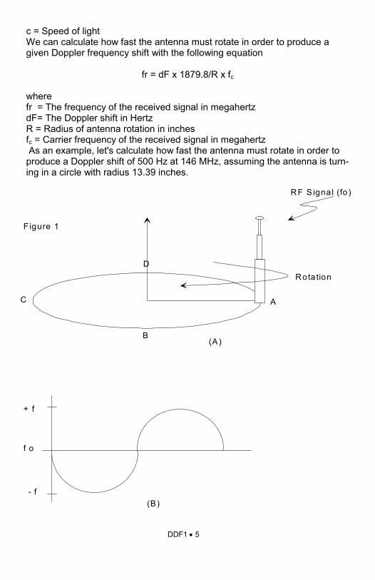
INTRODUCTION Radio direction finding is a fascinating hobby that has been becoming more and more popular in today's portable world. More recently, Doppler “df-ing” has become the rage, with a display that gives you a direct bearing on the lo-cation of the transmitter. Pretty neat trick considering you don’t need multiple separate receivers at different locations to triangulate on the mystery trans-mitter. DDF1 CIRCUIT DESCRIPTION The classic example of the Doppler effect is that of a car approaching a sta-tionary observer. The car's horn sounds higher in pitch (frequency) to an ob-server as the car approaches. The change in frequency occurs because the motion of the car shortens the wavelength. The horn sounds lower in pitch (frequency) to the observer as the car speeds away. This occurs because the car is speeding away from the observer effectively increasing the wave-length. Fewer cycles per second, hence, lower-frequency sound. A similar effect occurs when an antenna is moved toward or away from a transmitting source. The signal received from an antenna moving toward the transmitting source appears to be at a higher frequency than that of the actual transmis-sion. The signal received from an antenna moving away from the source of transmission appears to be lower in frequency than that of the actual trans-mission. Imagine a receiving antenna moving in a circular pattern as pic-tured in Figure 1A. Consider the antenna at position A, nearest the source of transmission. The frequency of the received signal at point A equals that of the transmitted signal because the antenna is not moving toward or away from the source of transmission. The frequency of the received signal de-creases as the antenna moves from point A to point B and from point B to point C. Maximum frequency deviation occurs as the antenna passes through point B. The frequency of the received signal at point C is the same as that of the transmitted signal (no shift) because the antenna is not moving toward or away from the source of transmission. As the antenna moves from point C to point D and from point D back to point A, the frequency of the re-ceived signal increases. Maximum frequency deviation occurs again as the antenna passes through point D. The Doppler frequency shift as a function of antenna rotation is illustrated in Figure 1B.
dF= ( rfc)/c where: dF =Peak change in frequency (Doppler shift in Hertz)
= Angular velocity of rotation in radians per second (2 x frequency of ro-tation) r = Radius of antenna rotation (meters) fc = Frequency of transmitted signal (Hertz)
DDF1 • 5
c = Speed of light We can calculate how fast the antenna must rotate in order to produce a given Doppler frequency shift with the following equation
fr = dF x 1879.8/R x fc where fr = The frequency of the received signal in megahertz dF= The Doppler shift in Hertz R = Radius of antenna rotation in inches fc = Carrier frequency of the received signal in megahertz As an example, let's calculate how fast the antenna must rotate in order to produce a Doppler shift of 500 Hz at 146 MHz, assuming the antenna is turn-ing in a circle with radius 13.39 inches.
RF S ignal (fo )
A
B
C
DRotation
f o
+ f
- f(B)
(A)
F igure 1
DDF1 • 6
The frequency of rotation is:
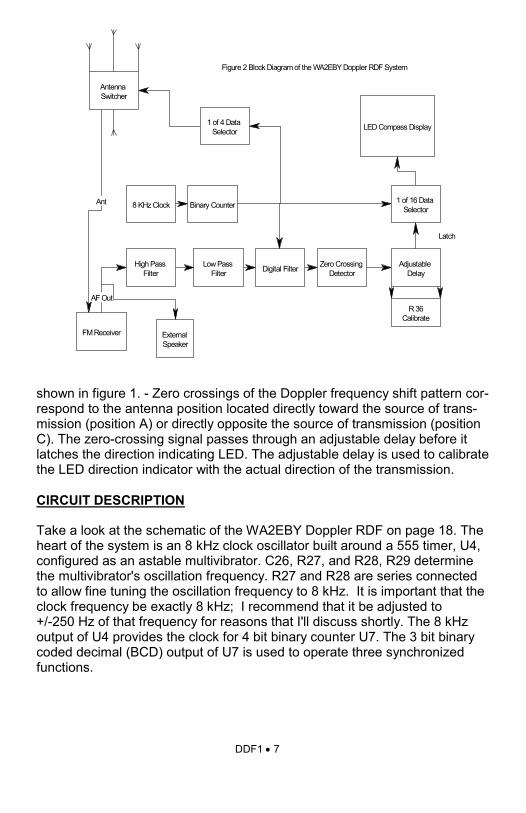
fr = 500 x 1879.8/146 x 13.39 A rotation frequency of 480 Hz translates to 480 x 60 = 28,800 or almost 30,000 r/min, which pretty much rules out any ideas of mechanically rotating the antenna! Fortunately, Terrence Rogers, WA4BVY, proposed a clever method of electrically spinning the antenna that works very well. Roger's pro-ject, the DoppleScAnt, uses eight 1/4- vertical whips arranged in a circular pattern. Only one antenna at a time is electrically selected. By controlling the order in which the antennas are selected, the DoppleScAnt emulates a sin-gle 1/4 – whip antenna moving in a circle. A clever feature in Roger's de-sign is the use of a digital audio filter to extract the Doppler tone from voice, PL tones and noise. The DDF1 design offers slightly improved audio filtering, 74HC-series logic circuits capable of driving the LED display directly, a wideband VHF/UHF an-tenna switcher and the four 1/4- mag-mount antennas. Total project cost is about one third the cost of purchasing a commercial RDF unit - and building the project is a lot more educational. HOW IT WORKS To understand the operation of the Doppler RDF circuit, see the block dia-gram of Figure 2. An 8 kHz clock oscillator drives a binary counter. The out-put of the counter performs three synchronized functions: "spin" the antenna, drive the LED display and run the digital filter. The counter output drives a 1 of 4 multiplexer that spins the antennas by sequentially selecting (turning on) one at a time in the order A,B,C,D,A, etc., at 500 times per second. The counter output also drives a 1 of 6 multiplexer used to drive the LED display in sync with the spinning antenna. The RF signal received from the spinning antenna is connected to the antenna input of a VHF or UHF FM receiver. The spinning antenna imposes a 500 Hz frequency deviation on a 146 MHz received signal. A 146 MHz FM receiver connected to the spinning an-tenna's RF output demodulates the 500 Hz frequency deviation and sounds like a 500 Hz tone with loudness set by the 500 Hz frequency deviation. The receiver audio, including 500 Hz Doppler tone, is processed by a series of audio filters. A high pass filter rejects PL tones and audio frequencies below the 500 Hz Doppler tone. A low-pass filter rejects all audio frequencies above the 500 Hz Doppler tone, and a very narrow bandwidth digital filter ex-tracts only 500 HZ Doppler tone. The output of the digital filter represents the actual Doppler frequency shift
DDF1 • 7
shown in figure 1. - Zero crossings of the Doppler frequency shift pattern cor-respond to the antenna position located directly toward the source of trans-mission (position A) or directly opposite the source of transmission (position C). The zero-crossing signal passes through an adjustable delay before it latches the direction indicating LED. The adjustable delay is used to calibrate the LED direction indicator with the actual direction of the transmission. CIRCUIT DESCRIPTION Take a look at the schematic of the WA2EBY Doppler RDF on page 18. The heart of the system is an 8 kHz clock oscillator built around a 555 timer, U4, configured as an astable multivibrator. C26, R27, and R28, R29 determine the multivibrator's oscillation frequency. R27 and R28 are series connected to allow fine tuning the oscillation frequency to 8 kHz. It is important that the clock frequency be exactly 8 kHz; I recommend that it be adjusted to +/-250 Hz of that frequency for reasons that I'll discuss shortly. The 8 kHz output of U4 provides the clock for 4 bit binary counter U7. The 3 bit binary coded decimal (BCD) output of U7 is used to operate three synchronized functions.
8 KHz Clock Binary Counter
Digital FilterLow Pass Filter
High Pass Filter
Zero Crossing Detector
Adjustable Delay
1 of 16 Data Selector
LED Compass Display1 of 4 Data Selector
FM Receiver
Latch
Antenna Switcher
External Speaker
Ant
AF OutR 36
Calibrate
Figure 2 Block Diagram of the WA2EBY Doppler RDF System
DDF1 • 8
Three Synchronized Functions The first function derived from binary counter U7 is antenna array spinning. This is accomplished by using the two most significant bits of U7 to run 1 of 4 multiplexer U8. The selected output of U8 (active low) is inverted by buffer U12. The buffered output of U12 (active high) supplies current sufficient to turn on the antenna to which it is connected. (The details of how this is done will be covered later.) Buffer outputs U12A, U12B, U12C and U12D are se-quenced in order. The corresponding buffer selects antennas A,B,C,D,A,B, etc. Driving multiplexer U8 with the two most significant bits of counter U7 di-vides the 8 kHz clock by four, so each antenna is turned on for 0.5 ms. One complete spin of the antenna requires 0.5 ms x 4 = 2.0 ms, thus the fre-quency of rotation is 2 ms or 500 Hz. An FM receiver connected to the spin-ning antenna's RF output has a 500 Hz tone imposed on the received signal. Sequencing the 16 LED display is the second synchronized function from bi-nary counter U7. This is done by using the binary output of counter U7 to se-lect 1 of 16 data outputs of U11. The selected output of U11 goes low, allow-ing current to flow from the +5 V supply through current limiting resistor R51, green center LED D16, and direction indicating red LED's D17 through D32. Each antenna remains turned on as the LED display sequences through four direction indicating LED's, then switches to the next antenna. Each direction indicating LED represents a heading change of 22.5 degrees. The third synchronized function is operating the digital filter responsible for extracting the Doppler tone. The 500 Hz Doppler tone present on the re-ceiver audio output is connected to an external speaker and audio level ad-just potentiometer R50. The signal is filtered by a two-pole Sallen Key high pass filter built around op amp U1A. It filters out PL tones and audio frequen-cies below the 500 Hz Doppler tone. Next, a four-pole Sallen-Key low pass filter using U1B and U1C band limits audio frequencies above the 500 Hz Doppler tone. The band limited signal is then applied to the input of a digital filter consisting of analog multiplexer U5, R18, R19 and C10 through C17. (Readers interested in the detailed operation and analysis of this fascinating digital filter are encouraged to review QEX magazine for June 1999) The Digital Filter Using the three most significant bits of U7 to drive the digital filter divides the 8 kHz clock by the two, making the digital filter code rate 4 kHz. The center frequency of the digital filter is determined solely by the clock frequency di-vided by the order of the filter. This is an 8th order filter, which makes the center frequency of the filter 4 kHz/8 =500 Hz. This is the exact frequency at which the antenna spins, hence, the same frequency of the Doppler tone produced on the receiver audio connected to the spinning antenna. This is
DDF1 • 9
truly an elegant feature of the Doppler RDF design. Using the same clock os-cillator to spin the antenna and clock the digital filter ensures the Doppler tone produced by the spinning process is precisely the center frequency of the digital filter. Even if the clock oscillator frequency drifts, the Doppler tone drifts accordingly, but the center frequency of the digital filter follows it pre-cisely because the same clock runs it. Excessive drift in the 8 kHz clock should be avoided, however, because the analog high and low pass filters that precede the digital filter have fixed passband centers of 500 Hz. A drift of +250 Hz on the 8 kHz clock corresponds to +62.5 Hz (250/4) drift in the Doppler tone produced. This value is acceptable because of the relatively low Q of the analog bandpass filter. Digital filter Q is calculated by dividing the filter's center frequency by its bandwidth (Q=f/BW) or 500 Hz/4 Hz=125. It's very difficult to realize such a high Q filter with active or passive analog filters and even more difficult to maintain a precise center frequency. The slightest change in temperature or component tolerance would easily de-Q or detune such filters from the de-sired 500 Hz Doppler tone frequency. The digital filter makes the high Q pos-sible and does so without the need for precision tolerance components. By varying damping pot R19, the response time of the digital filter is changed. This digital filter damping helps average rapid Doppler tone changes caused by multipath reflected signals, noise or high audio peaks associated with speech. A digitized representation of the Doppler tone is provided at the digi-tal filter output. A two pole Sallen Key low pass filter built around U2B filters out the digital steps in the waveform providing a near sinusoidal output corre-sponding to the Doppler shift illustrated in Figure 1B. The zero crossings of this signal indicate exactly when the Doppler effect is zero. Zero crossings are detected by U2C and used to fire a monostable multivibrator (U6) built around a 555 timer. U6's output latches the red LED in the display corre-sponding to the direction of transmission with respect to the green center LED, D16. Calibration between the actual source of transmission and the red direction indicating LED latched in the display is easily accomplished by changing the delay between the Doppler tone zero crossing (firing of U6) and the generation of the latch pulse to U11. C23, R36 and R37 determine this delay. Increasing or decreasing the delay is achieved by increasing or de-creasing the value of the calibrate potentiometer R36. Low Signal Level and Audio Overload Indicators Two useful modifications included in this design are the low signal level lock-out and audio overload indicators. U2D continuously monitors the amplitude of the Doppler tone at the input to the zero crossing detector. U2D’s output goes low whenever the Doppler tone amplitude drops below 0.11 V peak. This is done by referencing the negative input of U2D to 2.39 V, 0.11 V be-low the nominal 2.5 VDC reference level output of U2B by means of voltage
DDF1 • 10
divider, R21 and R22. U2D's output remains high when the Doppler tone is present and above 0.11 V peak. C9 discharges via D2 whenever U2D goes low, causing U3's output (pin 7) to go high, turning on Q2 via R24 and illumi-nating low signal level LED, D4. D4 remains on until the Doppler tone returns with amplitude above 0.11 V peak and C9 recharges via R23. The LED dis-play remains locked by disabling U11's strobe input whenever the Doppler tone is too low for an accurate bearing. This is done by pulling pin 1 of U11 low via D5 when Q2 is turned on. Audio overload indicator D3 tells you that audio clipping of the Doppler tone is occurring. Clipping results if the signal level from the digital filter is too high and can produce an erroneous bearing indication. The output of U1D goes low whenever the output of the digital filter drops below 0.6 V as the ampli-tude of the Doppler tone approaches the 0V supply rail. C7 discharges via D1 and causes the output of U3C to go high, turning on Q1 via R16 and illu-minating audio overload LED D3. We elected not to lock the LED display on audio overload; doing so, however, only requires connecting a diode be-tween the collector of Q1 and pin 1 of U11, similar to the low level lock out function. Phase Correction If the audio output of the Doppler RDF FM receiver is incorrectly phased, S3, phase invert, can fix that. (If phasing is incorrect, LED direction indications are 180 degrees opposite that of the actual signal source.) Moving S3 to the opposite position corrects the problem by letting U2C sense the trailing edge. This is particularly useful when switching between different receivers. S2 dis-ables the 8 kHz clock to disable the antenna spinning. This helps when you're trying to listen to the received signal. Presence of the Doppler tone in the received audio makes it difficult to understand what is being said, espe-cially with weak signals. Power Supply Power is delivered via on/off switch S1. D6 provides supply voltage reverse polarity protection by limiting the reverse voltage to 0.7 V. U10 provides a regulated 5 VDC to all digital ICs. C29 through C33 are bypass filters. U10's 5 VDC output is dropped 2.5 V by resistive divider R43 and R45. Non-inverting voltage follower U3B buffers the 2.5 V source to provide a virtual ground reference for all analog filters and the digital filter. Using a virtual ground 2.5 V above circuit ground allows op amps to process analog signals without the need of a negative power supply voltage. Analog voltages swing from near 0 V to near +5 V with the virtual ground level right in the middle, 2.5 V.
DDF1 • 11
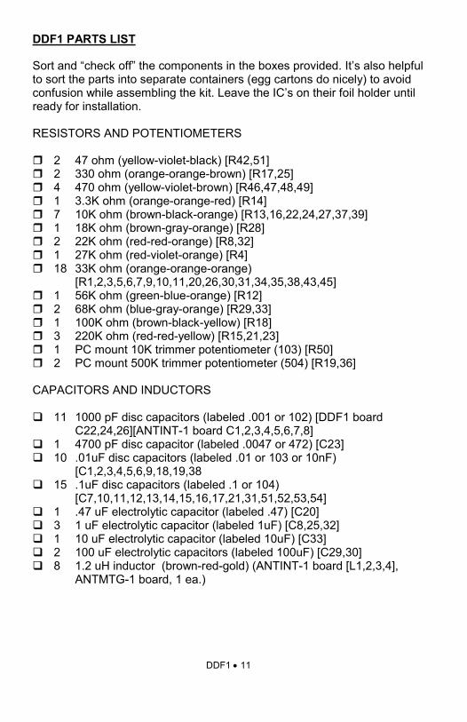
DDF1 PARTS LIST Sort and “check off” the components in the boxes provided. It’s also helpful to sort the parts into separate containers (egg cartons do nicely) to avoid confusion while assembling the kit. Leave the IC’s on their foil holder until ready for installation. RESISTORS AND POTENTIOMETERS
2 47 ohm (yellow-violet-black) [R42,51] 2 330 ohm (orange-orange-brown) [R17,25] 4 470 ohm (yellow-violet-brown) [R46,47,48,49] 1 3.3K ohm (orange-orange-red) [R14] 7 10K ohm (brown-black-orange) [R13,16,22,24,27,37,39] 1 18K ohm (brown-gray-orange) [R28] 2 22K ohm (red-red-orange) [R8,32] 1 27K ohm (red-violet-orange) [R4] 18 33K ohm (orange-orange-orange) [R1,2,3,5,6,7,9,10,11,20,26,30,31,34,35,38,43,45] 1 56K ohm (green-blue-orange) [R12] 2 68K ohm (blue-gray-orange) [R29,33] 1 100K ohm (brown-black-yellow) [R18] 3 220K ohm (red-red-yellow) [R15,21,23] 1 PC mount 10K trimmer potentiometer (103) [R50] 2 PC mount 500K trimmer potentiometer (504) [R19,36]
CAPACITORS AND INDUCTORS
11 1000 pF disc capacitors (labeled .001 or 102) [DDF1 board C22,24,26][ANTINT-1 board C1,2,3,4,5,6,7,8] 1 4700 pF disc capacitor (labeled .0047 or 472) [C23] 10 .01uF disc capacitors (labeled .01 or 103 or 10nF) [C1,2,3,4,5,6,9,18,19,38 15 .1uF disc capacitors (labeled .1 or 104) [C7,10,11,12,13,14,15,16,17,21,31,51,52,53,54] 1 .47 uF electrolytic capacitor (labeled .47) [C20] 3 1 uF electrolytic capacitor (labeled 1uF) [C8,25,32] 1 10 uF electrolytic capacitor (labeled 10uF) [C33] 2 100 uF electrolytic capacitors (labeled 100uF) [C29,30] 8 1.2 uH inductor (brown-red-gold) (ANTINT-1 board [L1,2,3,4], ANTMTG-1 board, 1 ea.)
DDF1 • 12
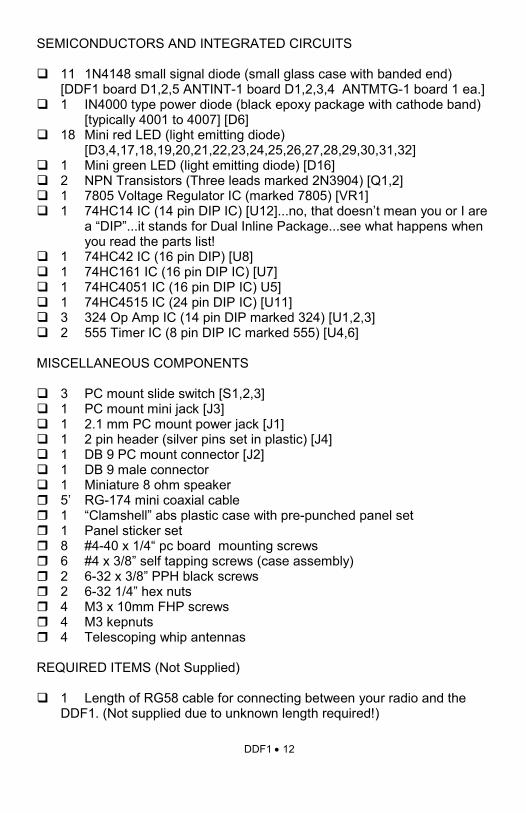
SEMICONDUCTORS AND INTEGRATED CIRCUITS
11 1N4148 small signal diode (small glass case with banded end) [DDF1 board D1,2,5 ANTINT-1 board D1,2,3,4 ANTMTG-1 board 1 ea.] 1 IN4000 type power diode (black epoxy package with cathode band) [typically 4001 to 4007] [D6] 18 Mini red LED (light emitting diode) [D3,4,17,18,19,20,21,22,23,24,25,26,27,28,29,30,31,32] 1 Mini green LED (light emitting diode) [D16] 2 NPN Transistors (Three leads marked 2N3904) [Q1,2] 1 7805 Voltage Regulator IC (marked 7805) [VR1] 1 74HC14 IC (14 pin DIP IC) [U12]...no, that doesn’t mean you or I are a “DIP”...it stands for Dual Inline Package...see what happens when you read the parts list! 1 74HC42 IC (16 pin DIP) [U8] 1 74HC161 IC (16 pin DIP IC) [U7] 1 74HC4051 IC (16 pin DIP IC) U5] 1 74HC4515 IC (24 pin DIP IC) [U11] 3 324 Op Amp IC (14 pin DIP marked 324) [U1,2,3] 2 555 Timer IC (8 pin DIP IC marked 555) [U4,6]
MISCELLANEOUS COMPONENTS
3 PC mount slide switch [S1,2,3] 1 PC mount mini jack [J3] 1 2.1 mm PC mount power jack [J1] 1 2 pin header (silver pins set in plastic) [J4] 1 DB 9 PC mount connector [J2] 1 DB 9 male connector 1 Miniature 8 ohm speaker 5’ RG-174 mini coaxial cable 1 “Clamshell” abs plastic case with pre-punched panel set 1 Panel sticker set 8 #4-40 x 1/4“ pc board mounting screws 6 #4 x 3/8” self tapping screws (case assembly) 2 6-32 x 3/8” PPH black screws 2 6-32 1/4” hex nuts 4 M3 x 10mm FHP screws 4 M3 kepnuts 4 Telescoping whip antennas
REQUIRED ITEMS (Not Supplied)
1 Length of RG58 cable for connecting between your radio and the DDF1. (Not supplied due to unknown length required!)
DDF1 • 13
RAMSEY Learn-As-You-Build KIT ASSEMBLY There are numerous solder connections on the DDF1 printed circuit board. Therefore, PLEASE take us seriously when we say that good soldering is es-sential to the proper operation of your direction finder! • Use a 25-watt soldering pencil with a clean, sharp tip. • Use only rosin-core solder intended for electronics use. • Use bright lighting, a magnifying lamp or bench-style magnifier may
be helpful. • Do your work in stages, taking breaks to check your work. Carefully
brush away wire cuttings so they don't lodge between solder con-nections.
We have a two-fold "strategy" for the order of the following kit assembly steps. First, we install parts in physical relationship to each other, so there's minimal chance of inserting wires into wrong holes. Second, whenever possi-ble, we install in an order that fits our "Learn-As-You Build" Kit building phi-losophy. This entails describing the circuit that you are building, instead of just blindly installing components. We hope that this will not only make as-sembly of our kits easier, but help you to understand the circuit you’re con-structing. For each part, our word "install" always means these steps: 1. Pick the correct part value to start with. 2. Insert it into the correct PC board location. 3. Orient it correctly, follow the PC board drawing and the written directions for all parts - especially when there's a right way and a wrong way to solder it in. (Diode bands, electrolytic capacitor polar ity, transistor shapes, dotted or notched ends of IC's, and so forth.) 4. Solder all connections unless directed otherwise. Use enough heat and solder flow for clean, shiny, completed connections. 5. Trim or “nip” the excess component lead wire after soldering. Enough of that ... lets get started!
DDF1 • 14
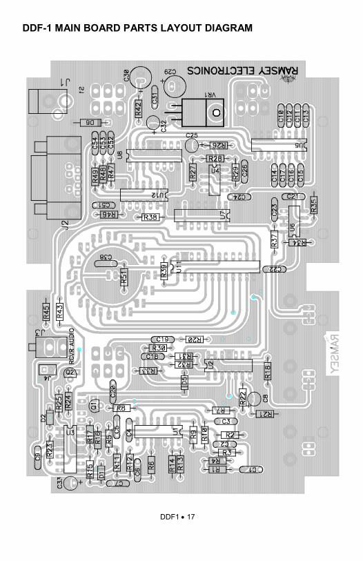
DDF1 DOPPLER DIRECTION FINDER ASSEMBLY STEPS Although we know that you are anxious to complete the assembly of your di-rection finder finder kit, it will become necessary to assemble in a specific or-der to accomplish the final components installation of your unit. Try to avoid the urge to “jump ahead” installing components. Please also note that the components will mount on BOTH SIDES OF THE PRINTED CIRCUIT BOARD for proper alignment into the provided case assembly. Since you may appreciate some “warm-up” soldering practice as well as a chance to put some “landmarks” on the PC board, we’ll first install some of the larger mounting components. This will also help us to get aquainted with the up - down, left - right orientation of the circuit board. Remember that the majority of the components will be mounted on the “component “ side of the circuit board and soldered on the “solder “ side of the circuit board, the side with the printed circuit traces. Have a look at the component layout diagram to help with your assembly.
1. Install J1, the 2.1 mm DC input connector. Notice that this mounts on the “component side of the circuit board and the solder leads push through the circuit board to protrude through the solder “pads” for con-nection. Be sure to push the part as close to the circuit board as it will go, as the alignment of this part is important in getting the case holes to line up with the part. Solder all three leads; don't be afraid to use enough heat to flow the entire connection.
2. Identify and install J3, the miniature audio input jack. Gently “rock” the component into place before soldering. Be sure to solder the mounting “tabs” into place to provide for a secure fit.
3. In the same manner, identify and install J2, the DB 9 connector, which will output the switching control voltage to the antenna switch. Be sure that the connector fits snugly to the printed circuit board. Solder all 11 connections to the jack, being careful not to “bridge” solder between the pins. Take your time here as a missed solder connection now can cause an hour of troubleshooting at the completion of your kit.
There we go, now we’re on our way to getting this one put together! Double check your connections, make sure that the jacks are resting snugly on the circuit board, and let’s continue. We’ll get started working on the clock sec-tion of our circuit, using a 555 oscillator IC.
4. Moving towards the lower right of the main circuit board (component side view), find the position for U4, one of the 555 timer IC’s. Install U4, the 555 timer IC. Make sure to align the notch or dot associated with pin one with the notch shown in the parts layout diagram. Also check to be
DDF1 • 15
sure all 8 pins are through the board before soldering the IC in place. This IC is responsible for the master clock oscillator for the direction finder unit , and replaces a few dozen discreet components.
5. Install C24, .001uF disc capacitor (marked 102).
6. Install R29, 68K ohm (blue-gray-orange).
7. Install R28, 18K ohm (brown-gray-orange).
8. Install C26, .001uF disc capacitor (marked 102).
9. Install R27, 10K ohm (brown-black-orange).
10. Install R26, 33K ohm (orange-orange-orange).
11. Identify C25, the 1 uF electrolytic capacitor. Electrolytic capacitors are polarized with a (+) and (-) lead and must be installed in the correct orientation. Ordinarily, only the negative side is marked on the capacitor body with a dark band and the (-) sign clearly shown, while the PC boards will usually show the (+) hole location. Use care to ensure proper polarity. See the parts diagram for proper placement. The capacitor should fit snugly down to the PC board.
Now it’s time to build the power supply regulation portion of the circuit. We need a well regulated low noise power supply to enable our circuit to work at peak performance.
12. Identify VR1, the 7805 voltage regulator IC. Install as shown in the diagram by carefully pre-bending the component leads at right angles to the regulator IC. The component should fit flush to the printed circuit board. Solder all three leads.
13. Install electrolytic capacitor C29, 100 uF. Again, this is an electrolytic capacitor and must be mounted with respect to the correct polarity.
14. In the same manner, install C32, 1 uF electrolytic. Watch that polar-ity!
15. Install C31, .1uF disc capacitor (marked 104).
16. Install R42, 47 ohm (yellow-violet-black).
17. Install C30, 100 uF electrolytic. Be sure to orient the polarity as shown in the diagram.
18. Identify D6, the 1N4002 diode (epoxy case with a polarity “band” de-
DDF1 • 16
noting the cathode (negative) side of the diode. Install as shown in the parts placement diagram (D6 is adjacent to the power switch S1).
19. Moving again towards the lower right of the main circuit board (component side view), find the position for U6, the other 555 timer IC. Install U6, the 555 timer IC. Make sure to align the notch or dot associ-ated with pin one with the notch shown in the parts layout diagram.
20. Install R34, 33K ohm (orange-orange-orange).
21. Install R35, 33K ohm (orange-orange-orange).
22. Install C21, .1uF disc capacitor (marked 104).
23. Install C23, .0047uF disc (marked .0047 or 472).
24. Install R37, 10K ohm (brown-black-orange).
25. Install C22, .001uF disc capacitor (marked 102). Now that wasn’t so bad was it! You’ve just completed the power supply and oscillator section of your direction finder. Pretty soon you will be searching for fox transmitters in baby strollers at the mall! Let’s get back to it. Next we’ll work on the digital filter section of the circuit. Be sure to mount the components as close to the printed circuit board as possible to provide for reliable operation.
26. Install C14,C17,C16,C15, all .1uF disc (marked 104). Now you're starting to roll along.
27. In the same manner, install C10, C12, C11, and C13, again, all .1uf (marked 104).
It is time to install some of the logic IC’s. Please note that although signifi-cant advances have been made in modern day CMOS technology, static precautions should be observed while installing these IC’s. Be sure to orient the IC band or notch as shown in the parts diagram for each IC. Try to focus on the individual IC pin as you’re soldering and “walk” the iron to consecutive pins of the IC as you continue.
28. Install U5, the 74HC4051 IC. Make sure not to “bridge” solder be-tween the pins.
29. Install U8, the 74HC42 IC. Solder all 16 pins.
30. Install U12, the 74HC14 inverter IC.
31. Install U7, 74HC161 IC. Watch that orientation!
DDF1 • 17
DDF-1 MAIN BOARD PARTS LAYOUT DIAGRAM

DDF1 • 18

DDF1 • 19
DDF1 • 20
32. Install U11, the 24 pin 74HC4515 IC. Make sure all the pins pass through the circuit board before e soldering.
Great job so far! Take a moment now to check your previous solder joints for “opens” where the solder did not completely flow around the connection or solder “bridges” between closely spaced pads or IC pins. It seems the best time to identify these types of problems is now when you’re focused on this section of the board, saving you time to try to rethink your steps later.
33. Install R39, 10K ohm (brown-black-orange).
34. Install R38, 33K ohm (orange-orange-orange).
35. Install R46, 470 ohm (yellow-violet-brown).
36. Install C51, .1uF disc (marked 104).
37. Install R47, 48, and 49, all 470 ohm (yellow-violet-brown).
38. Install disc capacitors C52, 53, and 54, all .1uF (marked 104). That concludes most of the digital circuitry included in your kit, take a mo-ment to recheck your work. We’ll get started now on the audio processing section of the direction finder kit.
39. Locate the position of C9 in the upper left hand corner of the main circuit board. Install C9, .01uF disc capacitor (marked .01 or 103 or 10nF).
40. Install R23, 220K ohm (red-red-yellow).
41. Identify D2, the 1N4148 small signal diode (marked with a polarity band). Use care to orient the part as shown in the parts diagram, and in-stall in the D2 position.
42. Install R25, 330 ohm (orange-orange-brown).
43. Install R24, 10K ohm (brown-black-orange).
44. Install speaker output jack J4 using the pin connector.
45. Identify and install Q2, the transistor marked 2N3904. The flat side must be placed as shown on the PC board, facing R24. Mount it as close to the board as possible without forcing it. Carefully solder all three leads.
46. Identify and install C33, a 10 uF electrolytic capacitor. Remember
DDF1 • 21
that electrolytics are polarized and must be mounted as shown in the diagram.
47. Install U3, the 324 op amp. Be sure to point the dot, notch, or band as shown in the parts diagram. Solder all 14 leads
48. Install R15, 220K ohm (red-red-yellow).
49. Install R17, 330 ohm (orange-orange-brown).
50. Moving to the right of J3, Install R43 and 45, both 33K ohm (orange-orange-orange).
51. Install transistor Q1, a 2N3904 type (marked 3904). Be sure to orient the flat side as shown in the parts diagram.
52. Identify and install small signal diode D1, 1N4148 (glass bead type with polarity band). Mount as shown in the parts layout diagram.
53. Install R16, 10K ohm (brown-black-orange). There is another plated through hole inside the silkscreen for R16 that is not the installation hole. Be sure to install the resistor lead in the proper hole.
54. Install C20, .47 uF electrolytic capacitor (marked .47). The banded (negative) side faces R8.
55. Install R8, 22K ohm (red-red-orange).
56. Install C4 and C5, both .01uF disc capacitors (marked .01 or 103).
57. Install R5, 33K ohm (orange-orange-orange).
58. Install R11, another 33K ohm (what were those colors)....(orange-orange-orange).
58. Install R12, 56K ohm (green-blue-orange).
59. Install C7, .1uF disc (marked 104).
60. Install C6, .01 disc capacitor (marked .01 or 103 or 10nF).
61. Install R6, 33K ohm (orange-orange-orange).
62. Install R14, 3.3K ohm (orange-orange-red).
63. Install R13, 10K ohm (brown-black-orange).
DDF1 • 22
64. Install a 324 Op amp in the U1 position, paying attention to the cor-rect part placement. Solder all 14 pins.
65. Install R9 and R10, both 33K ohm (orange-orange-orange).
66. Install R1, 33K ohm (orange-orange-orange).
67. Install R4, 27K ohm (red-violet-orange).
68. Install C1, .01uF (marked .01 or 103 or 10nF) .
69. Install R2,R3, and R7, all 33K ohm (orange-orange-orange).
70. Install C2 and C3, both .01uF (marked .01 or 103 or 10nF). Great going! You are really making progress now. Let’s finish up the compo-nents on the “component” side of the circuit board.
71. Install R21, 220K ohm (red-red-yellow).
72. Install R22, 10K ohm (brown-black-orange).
73. Install electrolytic capacitor C8 (1 uF). Be sure to orient the part cor-rectly.
74. Install R18, 100K ohm (brown-black-yellow).
75. Install the last 324 Op amp in the U2 position. Be sure to orient the part correctly before soldering.
76. Install D5, a 1N4148 diode. Again, observe the correct polarity for this part.
77. Install R32, 22K ohm (red-red-orange).
78. Install R31 and R20, both 33K ohm (orange-orange-orange).
79. Install R33, 68K ohm (blue-gray-orange).
80. Install C18 and 19, both .01uF (marked .01 or 103 or 10nF).
81. Install R30, 33K ohm (orange-orange-orange).
82. Moving to the right, install R51, 47 ohm (yellow-violet-black).
83 for the final component on the main board component side, install C38 (.01uF) (marked .01 or 103 or 10nF).
DDF1 • 23
Whew! Well, that's about it for the main circuit board assembly. Take a few minutes now to double check your work, especially the placement of the po-larized and orientation specific components. The next time we re-visit this board we’ll be ready to energize the circuit, so this is your last chance to “get it right the first time” and avoid timely circuit troubleshooting. Remember that time spent here can save a lot of time (and expense!) when the unit is initially turned on. In the final assembly steps for the DF main board, the components will be mounted to the SOLDER SIDE of the circuit board (aren’t you glad you didn’t jump ahead)! This will allow for correct orientation of the controls through the case assembly. These controls and displays will be the ones you’ll be look-ing at for years to come, so take your time to ensure proper positioning of each component.
84. Moving to the solder side of the circuit board, identify the locations for S1 (power), S2 (scan stop), and S3 (phase invert). Carefully insert the slide switches into position (one at a time is fine) in the S1, S2, and S3 positions. Ensure that each switch is mounted flush to the circuit board, and solder into place. The switches are DPDT type, so “up - down” orientation is not critical. Check the placement of each switch by “test fitting” the circuit board into the upper half of the case assembly and observing the switch position. Take care not to “skew” the switch as it may bind during normal operation.
85. Identify the 10K trimmer potentiometer (labeled 10K or 103 on the side of the pot). Note that the silkscreen for this part (and R19 and 36) is on the component side of the PC board. However, this part must be in-stalled on the solder side of the board. Install this potentiometer from the solder side of the circuit board in the R50 position. Check the parts placement diagram for correct placement if you are unsure. Make sure that this control is mounted flush to the circuit board and solder into place. Remember that you should be looking at a reverse image of the circuit board and that R50 is closest to the outside of the circuit board.
86. in the same manner, mount and install the two remaining potenti-ometers (500K ohms labeled 500K or 505) into the R19 and R36 posi-tion.
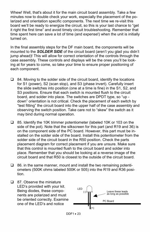
87. Observe the miniature LED’s provided with your kit. Being diodes, these compo-nents are polarized and must be oriented correctly. Examine one of the LED’s and notice
PC Board
LEDLeave these leads as long as possible
(+)
(-)
DDF1 • 24
how one lead is longer than the other. The longer of the two leads is the anode, or (+) connection. Most diodes also have a flat molded in the component body. This corresponds to the cathode or (-) side of the part. Note also that while both of the holes is rectangular, only one of the holes has the corners “rounded off“. The longer (anode) lead belongs in the “rounded off” hole, and the shorter (cathode) lead belongs in the rec-tangular (non-rounded) hole. Now for the fun part! When mounting the direction heading LED’s we would like the height of the diodes from the circuit board to be at just the correct height to protrude through the top panel of the unit. The easiest way to accomplish this task is to slide the LED’s into place making absolutely sure that the “flat” side of the diodes are correctly oriented as seen on the silkscreen. D3, 4, 17, 18, 19, 20, 21, 22, 23, 24, 25, 26, 27, 28, 29, 30, 31, 32 are RED LED’s , while D16 is the GREEN LED. Once the LED’s are loosely into place, temporarily fit the circuit board into the case top, and when tipped over the LED’s should fall into their respective holes.
88. With the 19 LED’s correctly oriented and set to the correct height, solder into place.
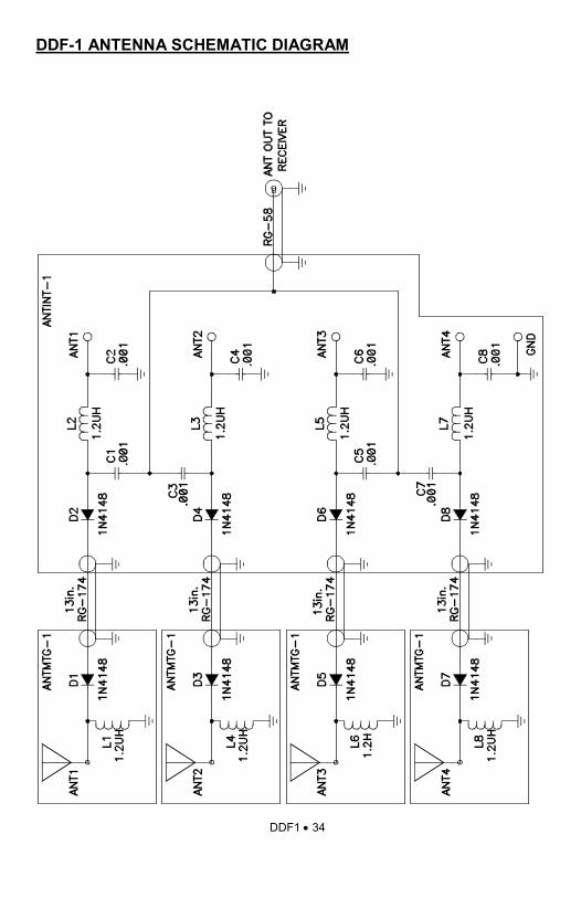
The main board assembly is complete! You are that much closer to a func-tioning Doppler DF system. Take a break...you have accomplished the big-gest “chunk” of the kit. When we start up again, we’ll be creating an antenna switching system for the direction finder ASSEMBLY INSTRUCTIONS FOR THE ANTENNA SYSTEM Roll those sleeves back up; we’ll get to the antenna switcher and individual antenna assemblies to complete the Doppler DF kit. Have a look at the ANTINT-1 antenna interface board. This is where we will accomplish the solid state switching between each antenna, Please note that this circuit board will be operating at RF frequencies; proper assembly tech-niques (i.e. short component lead lengths, coaxial cable connections ) will be critical on this board and the antenna assemblies. To minimize these imped-ance destroying lead lengths, we have opted for a “surface mount” proce-dure of the remaining components. Therefore instead of the typical “thru hole assembly“ you have completed on the main board, the components on this assembly will be soldered on the same side of the circuit board. It is neces-sary to preform the components and trim excess leads prior to the compo-nent being installed.
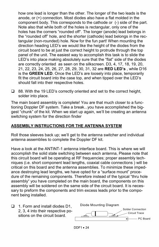
1. Form and install diodes D1, 2, 3, 4 into their respective po-sitions on the circuit board.
PC Board
Circuit TraceSolder Connection
Diode Mounting Diagram
DDF1 • 25
Use the shortest lead length possible. Note that these components are polarized. Install the banded end as shown in the parts diagram. Don’t worry about too much heat from your soldering iron; you will not damage the diodes.
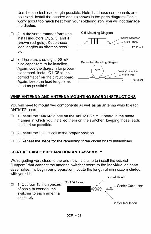
2. In the same manner form and install inductors L1, 2, 3, and 4 (brown-red-gold). Keep those lead lengths as short as possi-ble.
3. There are also eight .001uF disc capacitors to be installed. Again, see the diagram for proper placement. Install C1-C8 to the correct “tabs” on the circuit board. Again, keep the lead lengths as short as possible!
WHIP ANTENNA AND ANTENNA MOUNTING BOARD INSTRUCTIONS You will need to mount two components as well as an antenna whip to each ANTMTG board
1. Install the 1N4148 diode on the ANTMTG circuit board in the same manner in which you installed them on the switcher, keeping those leads as short as possible.
2. Install the 1.2 uH coil in the proper position.
3. Repeat the steps for the remaining three circuit board assemblies.
COAXIAL CABLE PREPARATION AND ASSEMBLY We’re getting very close to the end now! It is time to install the coaxial “jumpers” that connect the antenna switcher board to the individual antenna assemblies. To begin our preparation, locate the length of mini coax included with your kit.
1. Cut four 13 inch pieces of cable to connect the switcher to each antenna assembly.
PC Board
Circuit TraceSolder Connection
Coil Mounting Diagram
102
PC Board
Circuit TraceSolder Connection
Capacitor Mounting Diagram
RG-174 CoaxTinned Braid
Center Insulation
Center Conductor
DDF1 • 26
2. “Prep” each of the coaxial cables as shown in the diagram. Be careful not to use too much heat when “tinning” the braid of the coax as this could damage the center insulating shield.
3. Using some of your longer scrap resistor leads bent into a “U” shape, hold the coax into position and slide the “jumpers” through the provided mounting holes. These “jumpers” can be soldered on the bottom side of the board to hold the coax into position for final soldering.
4. Solder the coax center conductor to the circuit board, then apply a small fillet of solder to the braid. DO NOT USE TOO MUCH HEAT WHEN ATTACHING THE BRAID, as this can cause the center insulation of the cable to melt.
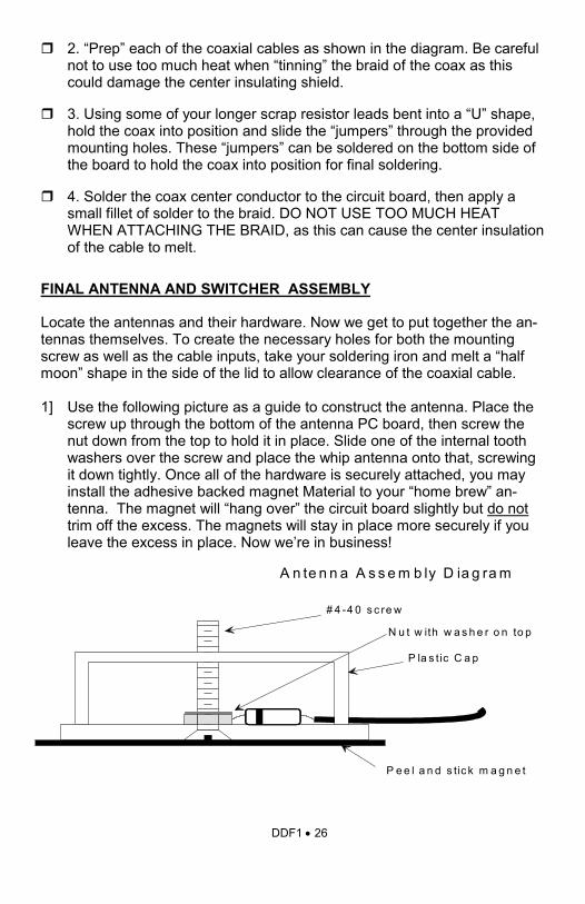
FINAL ANTENNA AND SWITCHER ASSEMBLY Locate the antennas and their hardware. Now we get to put together the an-tennas themselves. To create the necessary holes for both the mounting screw as well as the cable inputs, take your soldering iron and melt a “half moon” shape in the side of the lid to allow clearance of the coaxial cable. 1] Use the following picture as a guide to construct the antenna. Place the
screw up through the bottom of the antenna PC board, then screw the nut down from the top to hold it in place. Slide one of the internal tooth washers over the screw and place the whip antenna onto that, screwing it down tightly. Once all of the hardware is securely attached, you may install the adhesive backed magnet Material to your “home brew” an-tenna. The magnet will “hang over” the circuit board slightly but do not trim off the excess. The magnets will stay in place more securely if you leave the excess in place. Now we’re in business!
A n te n n a A s s e m b ly D ia g ra m
# 4 -4 0 s c re w
P la s t ic C a p
P e e l a n d s tic k m a g n e t
N u t w ith w a s h e r o n to p
DDF1 • 27
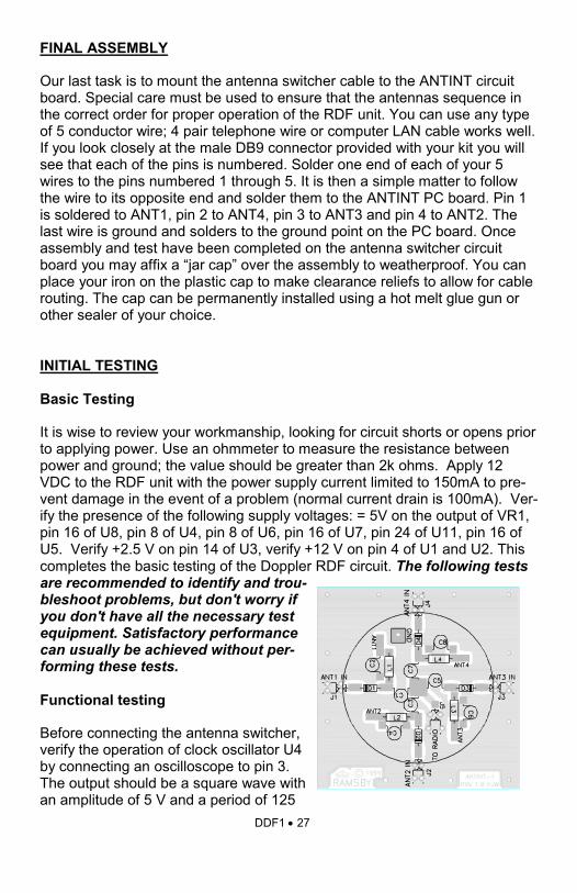
FINAL ASSEMBLY Our last task is to mount the antenna switcher cable to the ANTINT circuit board. Special care must be used to ensure that the antennas sequence in the correct order for proper operation of the RDF unit. You can use any type of 5 conductor wire; 4 pair telephone wire or computer LAN cable works well. If you look closely at the male DB9 connector provided with your kit you will see that each of the pins is numbered. Solder one end of each of your 5 wires to the pins numbered 1 through 5. It is then a simple matter to follow the wire to its opposite end and solder them to the ANTINT PC board. Pin 1 is soldered to ANT1, pin 2 to ANT4, pin 3 to ANT3 and pin 4 to ANT2. The last wire is ground and solders to the ground point on the PC board. Once assembly and test have been completed on the antenna switcher circuit board you may affix a “jar cap” over the assembly to weatherproof. You can place your iron on the plastic cap to make clearance reliefs to allow for cable routing. The cap can be permanently installed using a hot melt glue gun or other sealer of your choice. INITIAL TESTING Basic Testing It is wise to review your workmanship, looking for circuit shorts or opens prior to applying power. Use an ohmmeter to measure the resistance between power and ground; the value should be greater than 2k ohms. Apply 12 VDC to the RDF unit with the power supply current limited to 150mA to pre-vent damage in the event of a problem (normal current drain is 100mA). Ver-ify the presence of the following supply voltages: = 5V on the output of VR1, pin 16 of U8, pin 8 of U4, pin 8 of U6, pin 16 of U7, pin 24 of U11, pin 16 of U5. Verify +2.5 V on pin 14 of U3, verify +12 V on pin 4 of U1 and U2. This completes the basic testing of the Doppler RDF circuit. The following tests are recommended to identify and trou-bleshoot problems, but don't worry if you don't have all the necessary test equipment. Satisfactory performance can usually be achieved without per-forming these tests. Functional testing Before connecting the antenna switcher, verify the operation of clock oscillator U4 by connecting an oscilloscope to pin 3. The output should be a square wave with an amplitude of 5 V and a period of 125
DDF1 • 28
ms (8 kHz). Use a frequency counter to verify the clock frequency is 8 kHz +/- 250 Hz if you desire. Getting the clock frequency to exactly 8 kHz is not necessary for proper operation, however, the values of R27 and R28 can be changed to adjust the clock frequency. Verify that closing switch S2 disables the clock. Open S2 (scan stop) and verify the operation of BCD counter U7 by connecting the oscilloscope sequentially to pins 14,13,12, and 11. The signal frequency on these outputs should be approximately 4, 2, 1 and 0.5 kHz, respectively. Verify the presence of a square wave signal on pins 2,4,6 and 8 of buffer U12. Signal Level Indicators The following test uses an audio signal generator to simulate the presence of the Doppler tone. Disconnect the speaker from audio level control potenti-ometer R50 to prevent loading the signal generator. Connect an audio signal generator to the receiver audio input terminal. Set the generator to apply a 500 Hz sine wave with amplitude 1V P-P. Rotate R50 until the audio over-load LED D3 illuminates. Then, adjust R50 until low signal level LED D4 lights. Adjust R50 so that LEDs D3 and D4 are off, set calibrate control R36 to the center of its range and adjust damping control R19 for minimum damp-ing (fully CCW).
DDF1 • 29
Direction Indicator Adjust the frequency of the audio generator very slowly around 500 Hz while observing the LED display. You should see the direction indicating LEDs around the green center LED illuminating. The LED illumination should ro-tate clockwise when the frequency of the generator is set slightly lower than the antenna rotation frequency. (Only one LED will be on when the fre-quency of the generator equals the antenna rotation frequency.) The display should rotate counterclockwise. The audio generator must be capable of very fine frequency adjustment in order to observe the transition. All LED’s in the display may appear to be on if the signal generator frequency is just 10Hz different from that of the antenna rotation frequency determined by U4. It is interesting to observe the sharpness of the digital filter on pin 1 of U2 on the oscilloscope as the display makes the transition from counterclockwise. You can see the simulated Doppler tone of the generator come out of the noise, peak and return into the noise as the transition takes place. Calibration Control Verify the function of the calibrate control by adjusting the audio generator equal to the antenna rotation frequency. At this point, only a single LED will illuminate. Rotate the calibrate control through out its range and observe the direction indicating LED "move" around the display. The range of movement should be more than 360 degrees. The direction indicating LED may move slightly if the generator frequency drifts. It is very difficult to keep the gen-erator frequency synchronized exactly, but that's not necessary in this test. Disconnect the signal generator and reconnect the speaker to the receiver audio input terminal. Antenna Switcher Verifying proper operation of the antenna switcher sequencing circuit re-quires only a DC voltmeter. Connect the antenna switcher to the Doppler RDF unit and position the four mag-mount antennas on a table. Do not in-stall any of the whip antennas for this test. It is essential that the antenna be turned on in sequence to emulate an antenna spinning in a circular pattern for the Doppler RDF unit to operate correctly. A single antenna turned on out of sequence is enough to produce a bogus RDF reading. It does not matter if the antenna spins clockwise or counterclockwise.
DDF1 • 30
Scan/stop switch S2 stops the antenna from spinning. Close and open S2 until the voltage on terminal J2 pin 1 reads +5V. Pins 2, 3 and 4 should all read 0V. Pin 1 is the antenna enable signal for antenna 1. Label the corre-sponding mag mount antenna on the table as antenna 1. Close and open S2 until the voltage on terminal J2 pin 2 reads +5V. Pins 1,3, and 4 should all read 0V. Pin 2 is the antenna enable signal for antenna 4 and should be po-sitioned to the right of antenna 1 as viewed from the center of the antennas for a clockwise spin. Close and open S2 until the voltage on terminal J2 pin 3 reads +5V. Pins 1,2, and 4 should all read 0V. Pin 3 is the antenna enable signal for antenna 3 and should be positioned to the right of antenna 2 as viewed from the center of the antennas. Close and open S2 until the voltage on terminal J2 pin 4 reads +5V. Pins 1, 2, and 3 should all read 0V. Pin 4 is the antenna enable signal for antenna 2 and should be positioned to the right of antenna 3 as viewed from the center of the antennas. Testing the RF operation of the antenna is quite simple. Place all four mag mount antennas around the center of the car roof, placing each antenna at the corner of an 18.25 inch square pattern for operation on 146 MHz. Do not install any of the whip antennas yet. Connect the RF output of the antenna switcher to an FM receiver or transceiver tuned to a strong NOAA weather broadcast signal. Caution: Make sure you disable transmit mode if you are using a transceiver! Apply power to the RDF unit and open S2 to stop the spinning process. Take one whip antenna and touch it to the mounting screw on each of the mag mount antennas. Only one antenna should provide a signal strength reading similar to it being connected directly to the FM receiver. Remove the whip from the selected antenna and touch it to each of the other three anten-nas. The NOAA signal should be weak or nonexistent. Close and open S2 until another antenna is selected and repeat the same test. Continue the process until you have verified each antenna can be turned on while the other three remain off. Operation Checking performance of the RDF unit is best done in a large, empty area away from tall buildings: a parking lot will do. Use caution at all times during open road operation of the RDF unit. Use a minimum of two people for all testing and operation of the RDF unit: one to operate the vehicle and the other to operate the RDF unit. The magnets securing your antennas to the roof of the car were designed for use at reduced speeds. If you intend to use the DDF1 at highway speeds, you may want to get some stronger magnets.The powerful magnets contained in computer hard drives are excellent for this application and can often be found at flea markets or surplus store for as little as $1.00 or less. The typical magnet found in an audio speaker would
DDF1 • 31
also work well. As a safety measure, secure each PopTop Mag-Mount with 20 pound fishing line when operating the vehicle at highway speeds. Attach all four whip antennas to the mag-mount antenna bases placed about the center of the car top. Connect the RF output of the antenna switcher to a FM receiver transceiver tuned to a strong NOAA weather broadcast signal. Caution: Again, make sure you disable transmit mode if you are using a transceiver! It is best to use a smaller, handheld walkie talkie with your DDF1. The unit connects easily to the antenna on your handheld and be-cause they have less output power, there is less chance of doing damage by accidentally transmitting into your DDF1. Adjust the receiver's audio to a comfortable level in the external speaker. Apply 12 V to the RDF unit and “spin” the antenna by closing switch S2. As soon as S2 is closed, you should hear a 500 Hz tone imposed on the re-ceiver audio. Rotate audio level adjust control R50 so that low signal level LED D4 and audio overload LED D3 are extinguished. Never trust bearing indications if D3 and/or D4 are illuminated. The direction indicating display should be relatively constant with a single LED lit, or one or two adjacent LEDs alternately illuminating. Adjust calibrate control R36 so that the direc-tion indicating LED is consistent with the general direction of the NOAA transmission with respect to your location and the position of the car. Have the driver slowly circle while you observe the display. You should see the di-rection indicating LED move in the opposite direction as the car is turning in a circle. The position changes relative to the changing direction of the car, however, the direction indicated from the center of the circle the car is driving should remain fixed. If the display turns in the same direction as the car, flip phase invert switch S3 to the opposite position to correct the 180 degrees phasing offset. This completes the rough calibration procedure. Final Calibration A more accurate calibration can be achieved while the car is in motion. Posi-tion a volunteer with an HT in a safe spot on the side of a long, straight and vacant roadway about 1/4 to 1/2 mile away. Have them transmit on low power (up to 5W) while traveling towards them. The RDF operator should calibrate the RDF display to indicate 0 degrees as straight ahead. The dis-play should change to 180 degrees indicating the signal is coming from di-rectly behind the car as the vehicle passes the transmitter. The moving cali-bration producer functions to average out false reflected signals caused by multipath propagation. You may notice that the Doppler tone changes as the car moves about. The Doppler tone will sound like a pure, undistorted 500 Hz sine wave in the absence of reflected or multipath interference. Direction indications are most reliable under these conditions. When reflected or multi-path signals are present, the Doppler tone will sound raspy and distorted.
DDF1 • 32
Those signal components may arrive from different directions causing false bearing indications. The LED display tends to jump around randomly under these conditions. Avoid taking bearing information when the Doppler tone sounds raspy. You can minimize display jitter by slowing the response time of the digital filter. This is accomplished by increasing damping control R19. With a little time, you can master the art of Doppler RDFing. The wide bandwidth antenna switcher can be used for DFing on other bands, provided the proper antenna whip lengths and antenna spacing are used. Arrange the antennas in a square pattern. Typical antenna spacing for com-mon frequencies is shown in the table below. Whip lengths are measured from the top surface of the mag-mount PC board base to the tip of the anten-nas. You can determine the cor- rect an-tenna length for other frequencies by interpolation of values from the table above. The Doppler DF’er will work on virtually any VHF/UHF frequency! FINAL CASE UP When all your tests are complete, you will want to case up your main PC board. First, attach the overlay to the plastic case front. The best (only) way to do this is to spray the surface with a light coating of window cleaner. Next, peel the backing from the overlay and position it so that all the holes line up. At that point, smooth down the overlay with your fingers and leave the case top with the overlay properly positioned until the window cleaner evaporates. If you try to place the sticker on a dry surface and do not place it correctly the first time, you will be unable to remove the overlay without ruining it. Once the overlay is dry, you can attach the board to the case using the screws pro-vided. While you’re waiting you can attach the speaker to the case bottom using the screws included in your kit. The speaker fits over the holes drilled into the plastic case bottom. Insert the two screws into the holes in the case bottom and then place the speaker mounting holes through the screws. A nut on each screw will hold the speaker tight to the case bottom. Plug the
Frequency Antenna length in inches
146 MHz 18
223 MHz 13 1/2
446 MHz 7 7/8
DDF1 • 33
speaker into the 2 pin header and align the case top and bottom. Put a few more screws in place and you’re ready to roll. TROUBLESHOOTING INSTRUCTIONS While we had hoped that it wouldn’t come to this, if you are having trouble with your direction finder, here are a few suggestions. Use a methodical, logical troubleshooting technique. Most problems can be solved using common sense. A volt-ohm meter and a clear head are usually all that are needed to correct any problem. Most problems are due to mis-placed parts and/or bad solder connections. Working backwards through the assembly steps will often lead you to the problem. Please understand that it is nearly impossible to “troubleshoot” by phone, any specific questions should be documented and sent to us by mail. CONCLUSION We sincerely hope that you enjoy the use of this Ramsey product. As al-ways, we have tried to compose our manual in the easiest, most “user friendly” format that is possible. As our customers, we value your opinions, comments, and additions that you would like to see in future publications. Please submit comments or ideas to: Ramsey Electronics Inc. Attn. Hobby Kit Department 793 Canning Parkway Victor, NY 14564 And once again, thanks from the folks at Ramsey!
DDF1 • 34
DDF-1 ANTENNA SCHEMATIC DIAGRAM
DDF1 • 35
The Ramsey Kit Warranty Please read carefully BEFORE calling or writing in about your kit. Most problems can be solved without contacting the factory. Notice that this is not a "fine print" warranty. We want you to understand your rights and ours too! All Ramsey kits will work if assembled properly. The very fact that your kit includes this new manual is your assurance that a team of knowledgeable people have field-tested several "copies" of this kit straight from the Ramsey Inventory. If you need help, please read through your manual carefully, all information required to properly build and test your kit is contained within the pages! 1. DEFECTIVE PARTS: It's always easy to blame a part for a problem in your kit, Before you conclude that a part may be bad, thoroughly check your work. Today's semiconductors and passive components have reached incredibly high reliability levels, and its sad to say that our human construction skills have not! But on rare occasion a sour component can slip through. All our kit parts carry the Ramsey Electronics Warranty that they are free from defects for a full ninety (90) days from the date of purchase. Defective parts will be replaced promptly at our expense. If you suspect any part to be defective, please mail it to our factory for testing and replacement. Please send only the defective parts), not the entire kit. The parts) MUST be returned to us in suitable condition for testing. Please be aware that testing can usually determine if the part was truly defective or damaged by assembly or usage. Don't be afraid of telling us that you 'blew-it', we're all human and in most cases, replacement parts are very reasonably priced. 2. MISSING PARTS: Before assuming a part value is incorrect, check the parts listing carefully to see if it is a critical value such as a specific coil or IC, or whether a RANGE of values is suitable (such as "100 to 500 uF"). Often times, common sense will solve a mysterious missing part problem. If you're missing five 10K ohm resistors and received five extra 1K resistors, you can pretty much be assured that the '1K ohm' resistors are actually the 'missing' 10 K parts ("Hum-m-m, I guess the 'red' band really does look orange!") Ramsey Electronics project kits are packed with pride in the USA. If you believe we packed an incorrect part or omitted a part clearly indicated in your assembly manual as supplied with the basic kit by Ramsey, please write or call us with information on the part you need and proof of kit purchase. 3. FACTORY REPAIR OF ASSEMBLED KITS: To qualify for Ramsey Electronics factory repair, kits MUST: 1. NOT be assembled with acid core solder or flux. 2. NOT be modified in any manner. 3. BE returned in fully-assembled form, not partially assembled. 4. BE accompanied by the proper repair fee. No repair will be undertaken until we have received the MINIMUM repair fee (1/2 hour labor) of $25.00, or authorization to charge it to your credit card account. 5. INCLUDE a description of the problem and legible return address. DO NOT send a separate letter; include all correspondence with the unit. Please do not include your own hardware such as non-Ramsey cabinets, knobs, cables, external battery packs and the like. Ramsey Electronics, Inc., reserves the right to refuse repair on ANY item in which we find excessive problems or damage due to construction methods. To assist customers in such situations, Ramsey Electronics, Inc., reserves the right to solve their needs on a case-by-case basis. The repair is $50.00 per hour, regardless of the cost of the kit. Please understand that our technicians are not volunteers and that set-up, testing, diagnosis, repair and repacking and paperwork can take nearly an hour of paid employee time on even a simple kit. Of course, if we find that a part was defective in manufacture, there will be no charge to repair your kit (But please realize that our technicians know the difference between a defective part and parts burned out or damaged through improper use or assembly). 4. REFUNDS: You are given ten (10) days to examine our products. If you are not satisfied, you may return your unassembled kit with all the parts and instructions and proof of purchase to the factory for a full refund. The return package should be packed securely. Insurance is recommended. Please do not cause needless delays, read all information carefully.
DDF1 • 36
Doppler Radio Direction Finder Quick Reference Page Guide
Introduction to the DDF1 ................ 4 DDF1 Circuit Description ............... 4 Parts List .......................................11 DDF1 Assembly Steps ..................14 Component Layout .......................17 Schematic Diagram ......................18 Initial Testing .................................22 Ramsey Warranty .........................23
Price: $5.00 Ramsey Publication No. MDDF1 Instruction manual for: RAMSEY MODEL NO. DDF1 DOPPLER RADIO DIRECTION FINDER
RAMSEY ELECTRONICS, INC. 590 Fishers Station Drive Victor, New York 14564 Phone (585) 924-4560 Fax (585) 924-4555 www.ramseykits.com
REQUIRED TOOLS • Soldering Iron (WLC100) • Thin Rosin Core Solder (RTS12) • Needle Nose Pliers (MPP4 or RTS05) • Small Diagonal Cutters (RTS04) ADDITIONAL SUGGESTED ITEMS • Helping Hands Holder for PC Board/Parts (HH3) • Technician’s Tool Kit (TK405) • Desoldering Braid (RTS08)