Embed Size (px)
Citation preview
Radiation-Hard Detectors for Spectroscopy and Timing E. Berdermann*, D. Ackermann, M. Ciobanu, W. Hartmann, F. Heßberger, K. Hildenbrand,
S. Hofmann, M. Kiš , A. Martemiyanov, P. Moritz, M. Pomorski, M. Rebisz, B. Voss Gesellschaft für Schwerionenforschung (GSI) Darmstadt, Planckstr. 1, 64291 Darmstadt, Germany
A. G. Caragheorgheopol National Institute for Physics and Nuclear Engineering (NIPNE), POBox MG – 6,
76900 Bucharest- Magurele, Romania J. Morse, M. Salomé
European Synchrotron Radiation Facility (ESRF) Grenoble, 6 rue Jules Horowitz, BP220, 38043 Grenoble Cedex, France
B. Sulignano Institut für Kernchemie, Johannes Gutenberg University of Mainz, Postfach, D 55099 Mainz, Germany
A. Zhilin Institute for Theoretical and Experimental Physics (ITEP), Moscow,
B. Cheremushinskaja 25, Moscow 117259, Russia
for the NoRHDia* Collaboration
In the frame program of heavy-ion physics experiments electronic-grade PolyCrystalline diamond has been used for the development of large-area solid-state detectors able to work reliably in destructive heavy-ion beams. The success of all running diamond detectors at GSI is based upon the radiation hardness and response time of this type of material and on the huge ionisation signals produced by heavy ions. The intrinsic time resolution of 25 ps and the single-particle count-rate capability >5x10⁸ pps achieved are limited only by the bandwidth of available electronics. However, the inhibitive deep-trapping probability prevented the use of such devices for energy-loss spectroscopy, timing of minimum-ionizing particles, and any run with highly focused beams. Results of different SC CVD-diamond samples are discussed and compared with those of competitive detectors. The energy resolution is studied extensively, being a unique tool to assess the crucial material- and detector parameters simultaneously: the homogeneity and purity of the crystals and thus the uniformity of charge collection as well as of charge-carriers transport parameters, the existence or absence of traps and therefore the charge-collection efficiency including the risk of polarization effects and more. A relative resolution ∆E/Eα=0.003 is measured for 241Am-α-particles of Ea=5.486 MeV and ∆E/EC=0.01 for 12C ions of E1=43 MeV and E2=114 MeV, respectively. Both values are approaching silicon resolution (∆E/Eα=0.002, ∆E/EC=0.005). At operation bias, drift velocities vh ˜ 120 [µm/ns] respective ve ˜ 100 [µm/ns] are measured. Fitting the measured data range, common µ0
h ˜ 2330 [cm2/Vs] and vsat
h ˜ 1.4*107[cm/s] is obtained, where electron data show more spread and indicate different slopes for low- and high field values. A range 1400 < µ0
e [cm2/Vs] < 3100 but a single value for vsate ˜ 1.9*107
[cm/s] are computed. An intrinsic time resolution of 28 ps is obtained for both types of CVD-DDs in a beam test with relativistic 27Al ions of 54 GeV. New applications and perspectives for the implementation of both types of CVD diamond in upcoming low- and high-energy heavy-ion physics experiments are described.
1 Introduction This review is an assessment of CVD-Diamond (CVDD) for Heavy-Ion (HI) Physics detector applications requiring properties superior to those of PolyCrystalline CVDD Detectors (PC-DDs) [1-5]. Characteristic for Heavy-Ion (HI) collision physics are the wide range of colliding systems, kinetic energies and beam intensities covered, the latest varying from a few hundreds- up to 1013 particles/s (pps) focused down to 1mm diameter at target position. Transmission control by Beam- and Beam-Loss Monitors (BM) is essential, as beam losses state a serious radiation protection problem. Detectors, used as BM or Start (T0) detectors must be radiation hard, of fast response and of low material budget to maintain the brilliance of the beams and minimize background. Vertex detectors should have high spatial resolution and rate capability, as well as suitability to operate in magnetic fields. The projectile-target systems vary from p+p up to 238U+238U. Cryogenic energies of a few meV occur in ion traps, whereas particles from SPS at CERN, AGS and RHIC at BNL are of energies up to 40 TeV, corresponding to ion velocities of 98% the speed of light. The new
* Supported by the EU Integrated Infrastructure Initiative Hadron Physics, Project RII3-CT-2004-506078.
accelerator complex FAIR (Facility for Antiproton and Ion Research) to be built at GSI will deliver ions up to 30 GeV per atomic mass A, which is e.g. 7.14 TeV total kinetic energy for uranium ions of A=238 amu (atomic mass unit). The present machine complex operating at GSI in Darmstadt consists of a LINAC injector (UNILAC) up to Eprojectile = 11 A·MeV and a HI Synchrotron accelerator (SchwerIonenSynchrotron, SIS) up to Eproj = 2 A·GeV for light ions, Eproj = 1 A·GeV for the heaviest ions, and Eproj = 4 GeV for protons. Accelerated particles become relativistic at kinetic energies higher than their rest-mass equivalent A·Aproton (Aproton = 938 MeV), thus in case of Eproj = 1 A·GeV. Detectors for GSI experiments must be able to cope with low-energy elastic reactions, where the number of in- and outgoing particles is conserved and the heavy reaction products are stopped in the sensors, as well as with relativistic collisions, where the multiplicity per collision increases beyond 300 and the detectors become transparent for particles depositing only parts per billion of the ion's total kinetic energy. The event constituents are heavy fragments emitted from projectile- and target nuclei down to singly charged Minimum-Ionizing Particles (MIP) i.e. protons, electrons, pions and kaons as well as high-energy photons and neutrons. The dynamic range of energy-loss in the detectors is ~1:9000. Finally, rare processes are selected out of background reactions being 106-107 times more probable than the reaction of interest. It has been shown in the past [1][2][3] that PC CVD-diamond (PC-D) used 'As Grown' (AG) is excellent for a variety of HI applications, covering beam diagnostics, nuclear- and atomic physics experiments and radiotherapy with carbon ions as well. An overview of CVD-diamond applications developed at GSI up to the date of publication (2001) is given in Reference [4]. The versatility of PC-D, in conjunction with the high ionisation produced by HI balancing the reduced charge-collection probability, enables multi-task sensors operating simultaneously e.g. as beam-intensity, beam-profile and beam time-structure monitors as well as start detectors in experiments, or as online irradiation-profile monitors and ion-dosimeters in tumour therapy facilities. Since their rate capability ranges from single ions up to 109 pps in single-particle readout mode covering also higher beam intensities in integrating-current mode [5], beam diagnosis can be simplified and improved by replacing ensembles of beam-diagnostics detectors (ionisation chambers, plastic-scintillator detectors, wire chambers etc.), presently used to cover the full intensity range. Particular attention should be paid to the position-sensitive carbon-ion dosimeters [6] for the upgrade of the tumour-therapy facility at GSI [7]. Precise dose estimation is achieved by single-ion counting, reducing calibration uncertainties in integrated-current readout usually proposed for PC radiotherapy detectors [8]. However, the focus of this report is the characterisation of SC-CVD-Diamond (SC-D) for HI spectroscopy and MIP timing applications, where PC-DDs fail. The tested diamonds are exclusively supplied by Element Six, Ascot, UK. They are characterized in laboratories (offline) and in HI beams (online) and compared, if appropriate, to competitive state of the art detectors. New applications are introduced in sections 3.2.2 and 3.2.3 and a possible implementation of both types of DDs in the experiments projected for FAIR is described in sect. 5.
2 Sample and Contact Preparation Intense R&D on this issue is ongoing. Oxygen terminated samples are cleaned and metallized according to various protocols. The following preparation is currently applied:
o Cleaning of the samples with Aqua Regia (removing previous metallization, if any) o Boiling in H2SO4 + KNO3 for 30–60 min (oxidizing, removing graphite and carbides) o Rinsing in distilled-water ultrasonic bath o Drying with pure nitrogen gas o Storing in argon atmosphere until metallization o Application of sandwich-electrodes by evaporation or sputtering: Ti/Pt/Au (20nm/40nm/100nm), Cr/Au (50/100-200nm), Al(100nm) and Cr/Au-Ti/Pt/Au
on opposite surfaces. Standard for first tests is Cr/Au on both sides. o Annealing at 500oC; 10 min in argon atmosphere
As this is more adhesive, the metal layers on recent samples are sputtered. It is assumed that Schottky electrodes are formed by Al or Cr on CVD diamond [9], whereas carbide-forming Titanium forms 'Ohmic' electrodes. Aiming to separate bulk- from surface leakage current, an electrode configuration with a single-Guard Ring (GR) structure is tested in addition.
3 SC-D Material and Detector Performance The specifications of tested ?early’ (EBS) and ?recent’ (BDS) samples are listed in Table 1. Diamond IDs are repeated in case of multiple tests with different electrodes (see text).
Table 1. Specifications of Tested Samples EBS 1,2,3 BDS 5-14 BDS 9,10,13 BDS 10 Area [mm2] 12, 15, 9 25 17 - 21 25 Thickness [µm] 330, 300, 393 320-500 500 330 Contact ∅ [mm] 2.0, 2.5, 2.0 2.5 2.0 2.0 Metallisation Ti-Pt-Au
evaporated Cr/Au
sputtered Al
sputtered Al+GR
sputtered
3.1 Offline Characterisation
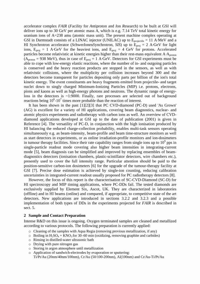
3.1.1 Dark-Current Characteristics Consecutive hysteretic measurements with Keithley electrometers are performed in a set up which consists of a Teflon barrel containing the polarized diamond sample to test, mounted inside an aluminium housing at ground potential. Due to three-pole measurements running in darkness and under nitrogen flow, parasitic currents caused by humidity or air ionization are minimized and distortion by pick-up is eliminated
Fig 1. Dark current behaviour of samples BDS 5-14 metallized with sputtered Cr-Au electrodes.
Fig. 1 shows the dark-current characteristics of the BDS samples in a glance, all obtained with sputtered Cr-Au electrodes. Low currents of absolute values < 10 picoamps are measured for samples 5, 6, 10, 12, 13 at E = +1 V/µm and for 5, 6, 7, 8, 10, 12, 13 at E = -1 V/µm. The measurements are performed in an electric-field range Emax = ± 3.0 V/µm by controlling dI/dV < 1nA/10V. These are currents, which are orders of magnitude lower than those obtained from PC-DD [10]. Nevertheless, the steep current increase in samples 7, 8, 11, 14 at
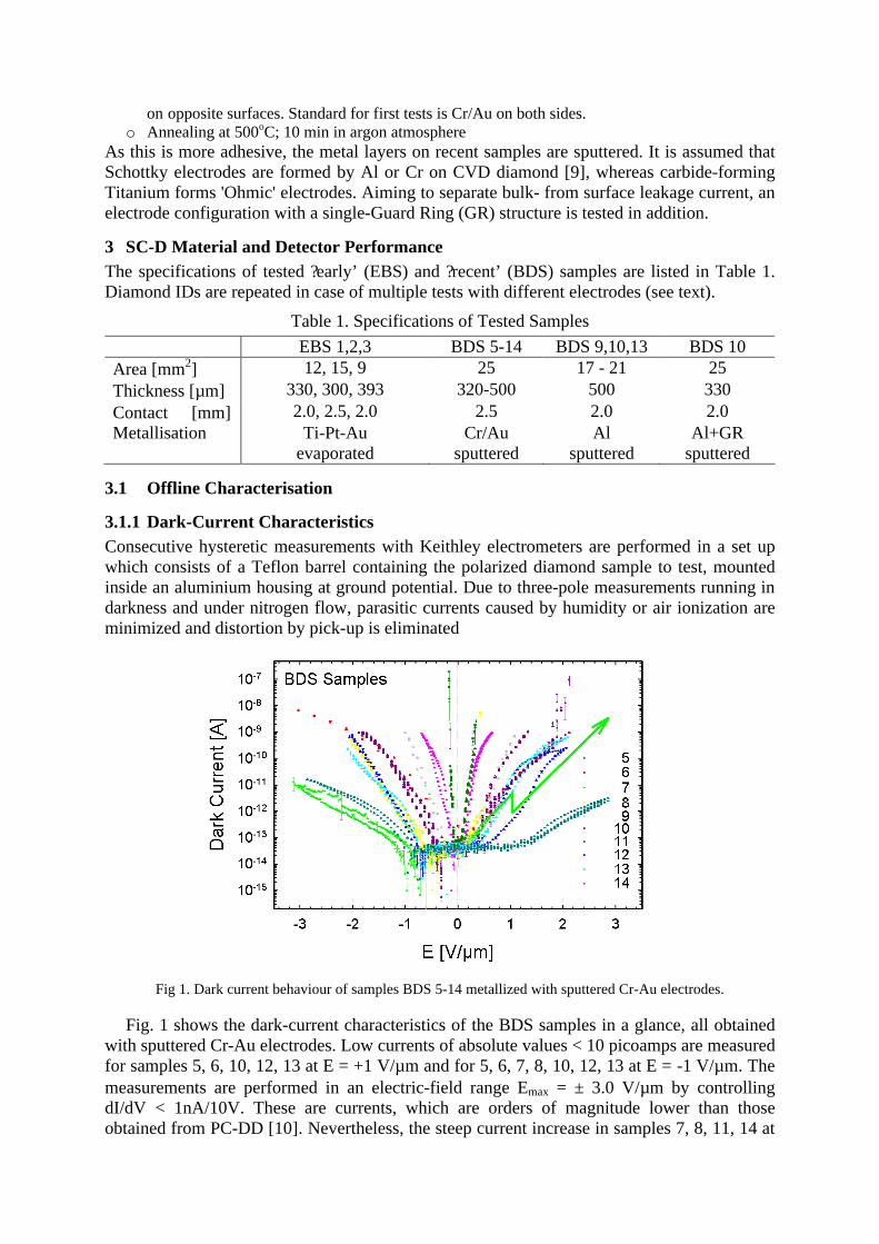
rather low positive bias is unexpected for material of resistivity > 1014 Ωcm. Moreover, real break down occurs occasionally (BDS 7 at +0.4 V/µm, BDS 8 at +0.5 V/µm, lightning bolts) followed by persistent hysteretic behaviour in some cases (Fig. 2, BDS 10 at positive bias).
Fig 2. Behaviour of different types of contacts (left graph) and of a GR structure (right graph). The dispersion of curve EBS 2 (left) may show a slightly different slope around zero potential. According to the
plot on the right, the measured currents are clearly not from surface leakage..
In the left plot of Fig. 2, X- and Y axis are zoomed in, to compare the dispersion of ?Ohmic’ (EBS 2,3) and ?Schottky’ (BDS 5,7,9,13) contacts. Precision measurements at such low current level are on the sensitivity limit of the electrometer. Positive offset and a weak linear slope of about 0.15pA/0.4V/µm, corresponding to 1015 Ω may be seen for sample EBS 2. Concerning the particle-detectors performance however, no difference was obtained neither in data of PC-DD equipped with either types of electrodes [4] nor for SC-DD as it will be demonstrated in the following. In the right plot, the effect of GR electrodes is tested on BDS 10. There is no influence obvious and thus, surface contributions may be excluded for this sample. However, bulk- and currents injected from the contacts are still ambiguous.
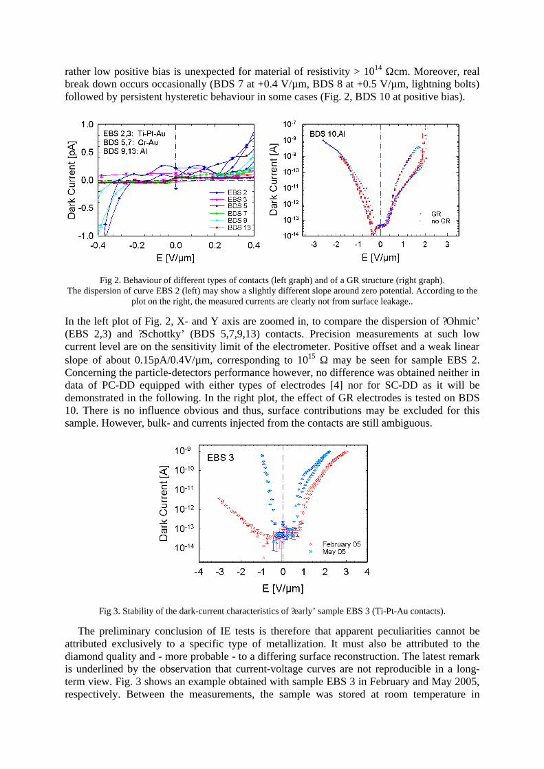
Fig 3. Stability of the dark-current characteristics of ?early’ sample EBS 3 (Ti-Pt-Au contacts).
The preliminary conclusion of IE tests is therefore that apparent peculiarities cannot be attributed exclusively to a specific type of metallization. It must also be attributed to the diamond quality and - more probable - to a differing surface reconstruction. The latest remark is underlined by the observation that current-voltage curves are not reproducible in a long-term view. Fig. 3 shows an example obtained with sample EBS 3 in February and May 2005, respectively. Between the measurements, the sample was stored at room temperature in
nitrogen gas and was not used for irradiation tests. The poor stability of the dark current is unlikely to be generated by bulk processes. Further work needs to be done in order to identify the interplay of different contributions.
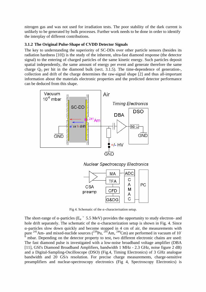
3.1.2 The Original Pulse-Shape of CVDD Detector Signals The key to understanding the superiority of SC-DDs over other particle sensors (besides its radiation hardness [10]) is the study of the inherent, ultra-fast diamond response (the detector signal) to the entering of charged particles of the same kinetic energy. Such particles deposit spatial independently, the same amount of energy per event and generate therefore the same charge QG per hit in the diamond bulk (sect. 3.1.5). The time-dependence of generation-, collection and drift of the charge determines the raw-signal shape [2] and thus all-important information about the materials electronic properties and the predicted detector performance can be deduced from this shape.
Fig 4. Schematic of the α-characterisation setup.
The short-range of α-particles (Eα ˜ 5.5 MeV) provides the opportunity to study electron- and hole drift separately. The schematic of the α-characterization setup is shown in Fig. 4. Since α-particles slow down quickly and become stopped in 4 cm of air, the measurements with pure 241Am- and mixed-nuclide sources (239Pu, 241Am, 244Cm) are performed in vacuum of 10-
6 mbar. Depending on the detector property to test, two different electronic chains are used: The fast diamond pulse is investigated with a low-noise broadband voltage amplifier (DBA [11], GSI's Diamond Broadband Amplifiers, bandwidth 1 MHz - 2.3 GHz, noise figure 2 dB) and a Digital-Sampling-Oscilloscope (DSO) (Fig.4, Timing Electronics) of 3 GHz analogue bandwidth and 20 GS/s resolution. For precise charge measurements, charge-sensitive preamplifiers and nuclear-spectroscopy electronics (Fig 4, Spectroscopy Electronics) is
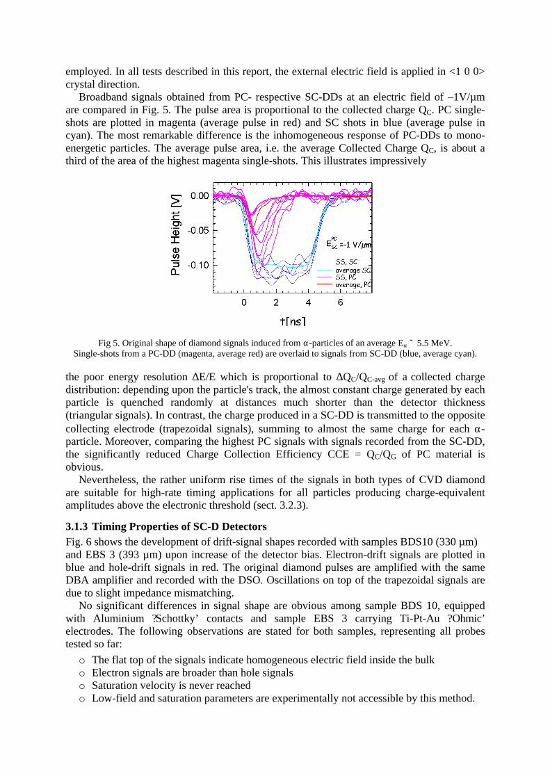
employed. In all tests described in this report, the external electric field is applied in <1 0 0> crystal direction. Broadband signals obtained from PC- respective SC-DDs at an electric field of –1V/µm are compared in Fig. 5. The pulse area is proportional to the collected charge QC. PC single-shots are plotted in magenta (average pulse in red) and SC shots in blue (average pulse in cyan). The most remarkable difference is the inhomogeneous response of PC-DDs to mono-energetic particles. The average pulse area, i.e. the average Collected Charge QC, is about a third of the area of the highest magenta single-shots. This illustrates impressively
Fig 5. Original shape of diamond signals induced from α-particles of an average Eα ˜ 5.5 MeV. Single-shots from a PC-DD (magenta, average red) are overlaid to signals from SC-DD (blue, average cyan).
the poor energy resolution ∆E/E which is proportional to ∆QC/QC-avg of a collected charge distribution: depending upon the particle's track, the almost constant charge generated by each particle is quenched randomly at distances much shorter than the detector thickness (triangular signals). In contrast, the charge produced in a SC-DD is transmitted to the opposite collecting electrode (trapezoidal signals), summing to almost the same charge for each α-particle. Moreover, comparing the highest PC signals with signals recorded from the SC-DD, the significantly reduced Charge Collection Efficiency CCE = QC/QG of PC material is obvious.
Nevertheless, the rather uniform rise times of the signals in both types of CVD diamond are suitable for high-rate timing applications for all particles producing charge-equivalent amplitudes above the electronic threshold (sect. 3.2.3).
3.1.3 Timing Properties of SC-D Detectors Fig. 6 shows the development of drift-signal shapes recorded with samples BDS10 (330 µm) and EBS 3 (393 µm) upon increase of the detector bias. Electron-drift signals are plotted in blue and hole-drift signals in red. The original diamond pulses are amplified with the same DBA amplifier and recorded with the DSO. Oscillations on top of the trapezoidal signals are due to slight impedance mismatching.
No significant differences in signal shape are obvious among sample BDS 10, equipped with Aluminium ?Schottky’ contacts and sample EBS 3 carrying Ti-Pt-Au ?Ohmic’ electrodes. The following observations are stated for both samples, representing all probes tested so far:
o The flat top of the signals indicate homogeneous electric field inside the bulk o Electron signals are broader than hole signals o Saturation velocity is never reached o Low-field and saturation parameters are experimentally not accessible by this method.
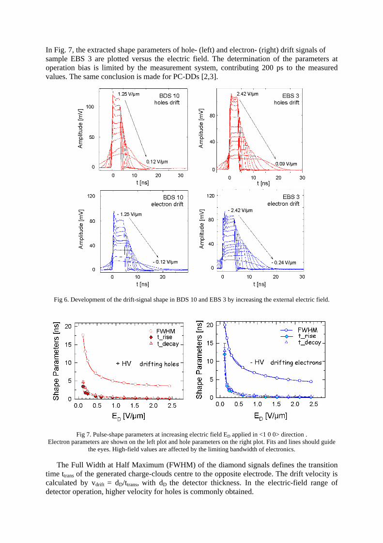
In Fig. 7, the extracted shape parameters of hole- (left) and electron- (right) drift signals of sample EBS 3 are plotted versus the electric field. The determination of the parameters at operation bias is limited by the measurement system, contributing 200 ps to the measured values. The same conclusion is made for PC-DDs [2,3].
Fig 6. Development of the drift-signal shape in BDS 10 and EBS 3 by increasing the external electric field.
Fig 7. Pulse-shape parameters at increasing electric field ED applied in <1 0 0> direction . Electron parameters are shown on the left plot and hole parameters on the right plot. Fits and lines should guide
the eyes. High-field values are affected by the limiting bandwidth of electronics.
The Full Width at Half Maximum (FWHM) of the diamond signals defines the transition time ttrans of the generated charge-clouds centre to the opposite electrode. The drift velocity is calculated by vdrift = dD/ttrans, with dD the detector thickness. In the electric-field range of detector operation, higher velocity for holes is commonly obtained.
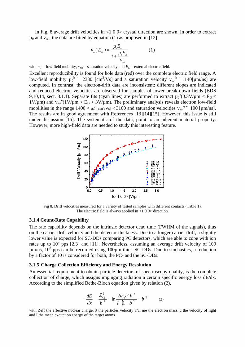
In Fig. 8 average drift velocities in <1 0 0> crystal direction are shown. In order to extract µ0 and vsat, the data are fitted by equation (1) as proposed in [12]
sat
D0
D0
Ddr
vEµ
1
Eµ)E(v
+= (1)
with µ0 = low-field mobility, vsat = saturation velocity and ED = external electric field.
Excellent reproducibility is found for hole data (red) over the complete electric field range. A low-field mobility µ0
h ˜ 2330 [cm2/Vs] and a saturation velocity vsath ˜ 140[µm/ns] are
computed. In contrast, the electron-drift data are inconsistent: different slopes are indicated and reduced electron velocities are observed for samples of lower break-down fields (BDS 9,10,14, sect. 3.1.1). Separate fits (cyan lines) are performed to extract µ0
e(0.3V/µm < ED < 1V/µm) and vsat
e(1V/µm < ED < 3V/µm). The preliminary analysis reveals electron low-field mobilities in the range 1400 < µ0
e [cm2/Vs] < 3100 and saturation velocities vsate ˜ 190 [µm/ns].
The results are in good agreement with References [13][14][15]. However, this issue is still under discussion [16]. The systematic of the data, point to an inherent material property. However, more high-field data are needed to study this interesting feature.
Fig 8. Drift velocities measured for a variety of tested samples with different contacts (Table 1). The electric field is always applied in <1 0 0> direction.
3.1.4 Count-Rate Capability The rate capability depends on the intrinsic detector dead time (FWHM of the signals), thus on the carrier drift velocity and the detector thickness. Due to a longer carrier drift, a slightly lower value is expected for SC-DDs comparing PC detectors, which are able to cope with ion rates up to 109 pps [2,3] and [11]. Nevertheless, assuming an average drift velocity of 100 µm/ns, 108 pps can be recorded using 100µm thick SC-DDs. Due to stochastics, a reduction by a factor of 10 is considered for both, the PC- and the SC-DDs.
3.1.5 Charge Collection Efficiency and Energy Resolution An essential requirement to obtain particle detectors of spectroscopy quality, is the complete collection of charge, which assigns impinging radiation a certain specific energy loss dE/dx. According to the simplified Bethe-Bloch equation given by relation (2),
( )
−
−⋅⋅∝− 2
2
22
2
2
12
ln βββ
β IcmZ
dxdE eeff
(2)
with Zeff the effective nuclear charge, β the particles velocity v/c, me the electron mass, c the velocity of light and I the mean excitation energy of the target atoms
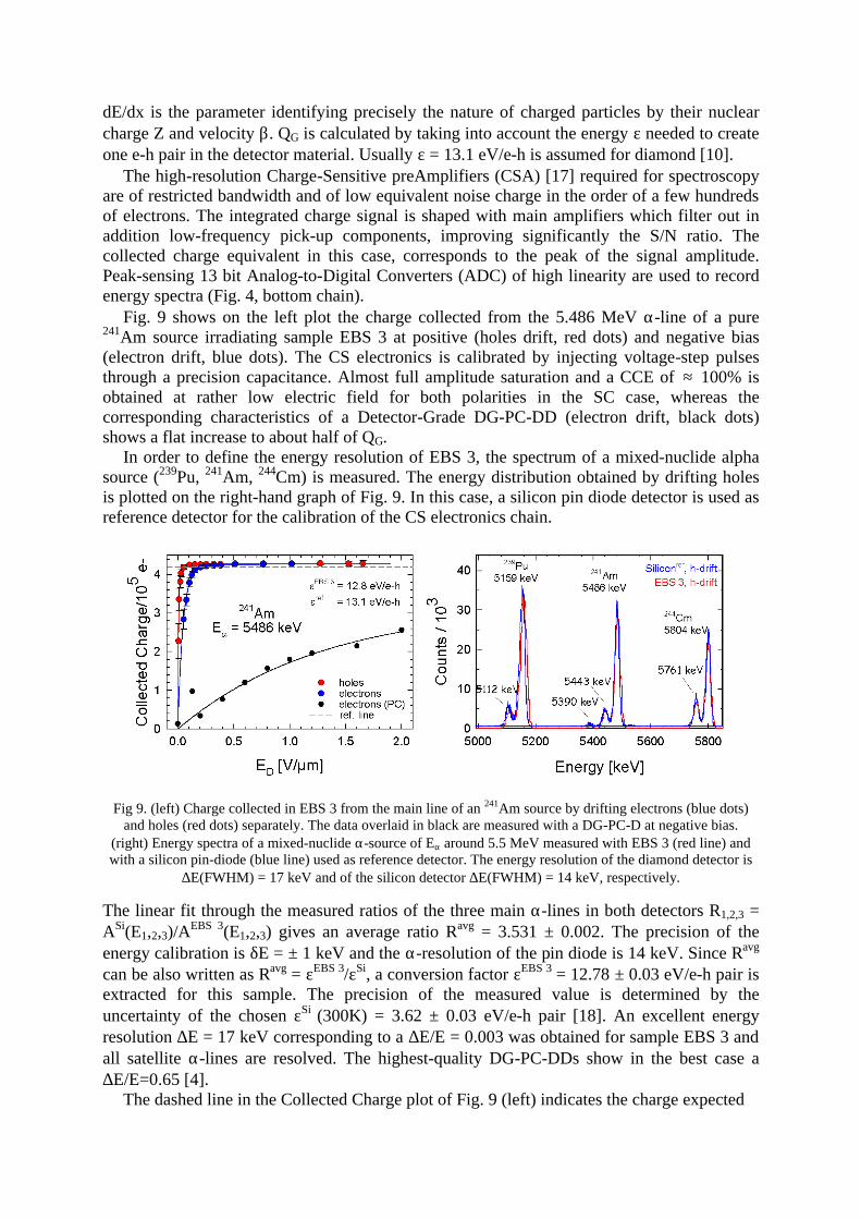
dE/dx is the parameter identifying precisely the nature of charged particles by their nuclear charge Z and velocity β. QG is calculated by taking into account the energy ε needed to create one e-h pair in the detector material. Usually ε = 13.1 eV/e-h is assumed for diamond [10]. The high-resolution Charge-Sensitive preAmplifiers (CSA) [17] required for spectroscopy are of restricted bandwidth and of low equivalent noise charge in the order of a few hundreds of electrons. The integrated charge signal is shaped with main amplifiers which filter out in addition low-frequency pick-up components, improving significantly the S/N ratio. The collected charge equivalent in this case, corresponds to the peak of the signal amplitude. Peak-sensing 13 bit Analog-to-Digital Converters (ADC) of high linearity are used to record energy spectra (Fig. 4, bottom chain). Fig. 9 shows on the left plot the charge collected from the 5.486 MeV α-line of a pure 241Am source irradiating sample EBS 3 at positive (holes drift, red dots) and negative bias (electron drift, blue dots). The CS electronics is calibrated by injecting voltage-step pulses through a precision capacitance. Almost full amplitude saturation and a CCE of ≈ 100% is obtained at rather low electric field for both polarities in the SC case, whereas the corresponding characteristics of a Detector-Grade DG-PC-DD (electron drift, black dots) shows a flat increase to about half of QG. In order to define the energy resolution of EBS 3, the spectrum of a mixed-nuclide alpha source (239Pu, 241Am, 244Cm) is measured. The energy distribution obtained by drifting holes is plotted on the right-hand graph of Fig. 9. In this case, a silicon pin diode detector is used as reference detector for the calibration of the CS electronics chain.
Fig 9. (left) Charge collected in EBS 3 from the main line of an 241Am source by drifting electrons (blue dots) and holes (red dots) separately. The data overlaid in black are measured with a DG-PC-D at negative bias.
(right) Energy spectra of a mixed-nuclide α-source of Eα around 5.5 MeV measured with EBS 3 (red line) and with a silicon pin-diode (blue line) used as reference detector. The energy resolution of the diamond detector is
∆E(FWHM) = 17 keV and of the silicon detector ∆E(FWHM) = 14 keV, respectively.
The linear fit through the measured ratios of the three main α-lines in both detectors R1,2,3 = ASi(E1,2,3)/AEBS 3(E1,2,3) gives an average ratio Ravg = 3.531 ± 0.002. The precision of the energy calibration is δE = ± 1 keV and the α-resolution of the pin diode is 14 keV. Since Ravg can be also written as Ravg = εEBS 3/εSi, a conversion factor εEBS 3 = 12.78 ± 0.03 eV/e-h pair is extracted for this sample. The precision of the measured value is determined by the uncertainty of the chosen εSi (300K) = 3.62 ± 0.03 eV/e-h pair [18]. An excellent energy resolution ∆E = 17 keV corresponding to a ∆E/E = 0.003 was obtained for sample EBS 3 and all satellite α-lines are resolved. The highest-quality DG-PC-DDs show in the best case a ∆E/E=0.65 [4]. The dashed line in the Collected Charge plot of Fig. 9 (left) indicates the charge expected
for εref = 13.1 eV/e-h. Obviously, this value is not valid for these data, which however are in perfect agreement with the conversion factor of εEBS 3 defined by the independent silicon calibration.
3.2 Online Characterisation
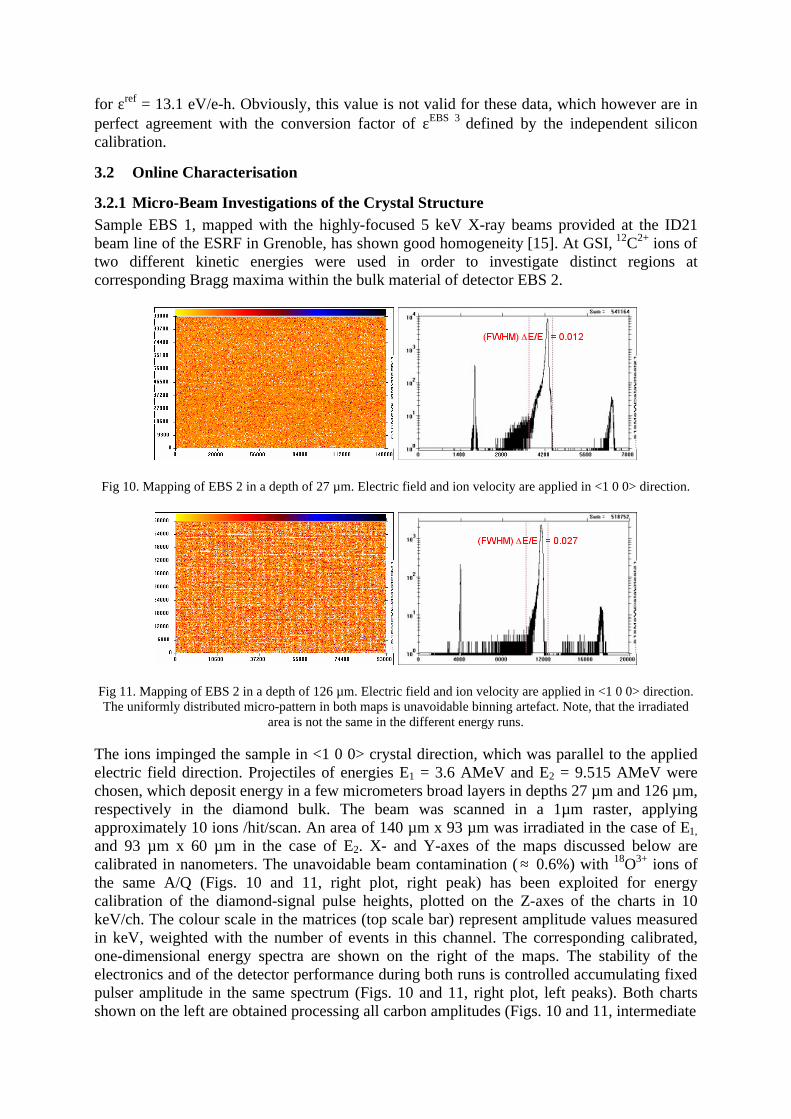
3.2.1 Micro-Beam Investigations of the Crystal Structure Sample EBS 1, mapped with the highly-focused 5 keV X-ray beams provided at the ID21 beam line of the ESRF in Grenoble, has shown good homogeneity [15]. At GSI, 12C2+ ions of two different kinetic energies were used in order to investigate distinct regions at corresponding Bragg maxima within the bulk material of detector EBS 2.
Fig 10. Mapping of EBS 2 in a depth of 27 µm. Electric field and ion velocity are applied in <1 0 0> direction.
Fig 11. Mapping of EBS 2 in a depth of 126 µm. Electric field and ion velocity are applied in <1 0 0> direction. The uniformly distributed micro-pattern in both maps is unavoidable binning artefact. Note, that the irradiated
area is not the same in the different energy runs.
The ions impinged the sample in <1 0 0> crystal direction, which was parallel to the applied electric field direction. Projectiles of energies E1 = 3.6 AMeV and E2 = 9.515 AMeV were chosen, which deposit energy in a few micrometers broad layers in depths 27 µm and 126 µm, respectively in the diamond bulk. The beam was scanned in a 1µm raster, applying approximately 10 ions /hit/scan. An area of 140 µm x 93 µm was irradiated in the case of E1, and 93 µm x 60 µm in the case of E2. X- and Y-axes of the maps discussed below are calibrated in nanometers. The unavoidable beam contamination ( ≈ 0.6%) with 18O3+ ions of the same A/Q (Figs. 10 and 11, right plot, right peak) has been exploited for energy calibration of the diamond-signal pulse heights, plotted on the Z-axes of the charts in 10 keV/ch. The colour scale in the matrices (top scale bar) represent amplitude values measured in keV, weighted with the number of events in this channel. The corresponding calibrated, one-dimensional energy spectra are shown on the right of the maps. The stability of the electronics and of the detector performance during both runs is controlled accumulating fixed pulser amplitude in the same spectrum (Figs. 10 and 11, right plot, left peaks). Both charts shown on the left are obtained processing all carbon amplitudes (Figs. 10 and 11, intermediate
peaks) as indicated in the corresponding spectra, shown for better clarity in logarithmic scale. The uniformly distributed micro-pattern is an unavoidable binning artefact. Apart from this, the pattern shows no features, i.e. evidence of the homogeneity of the bulk material. The energy loss of the ions in the metallization amounts to 290 keV for E1 and 167 keV for E2,
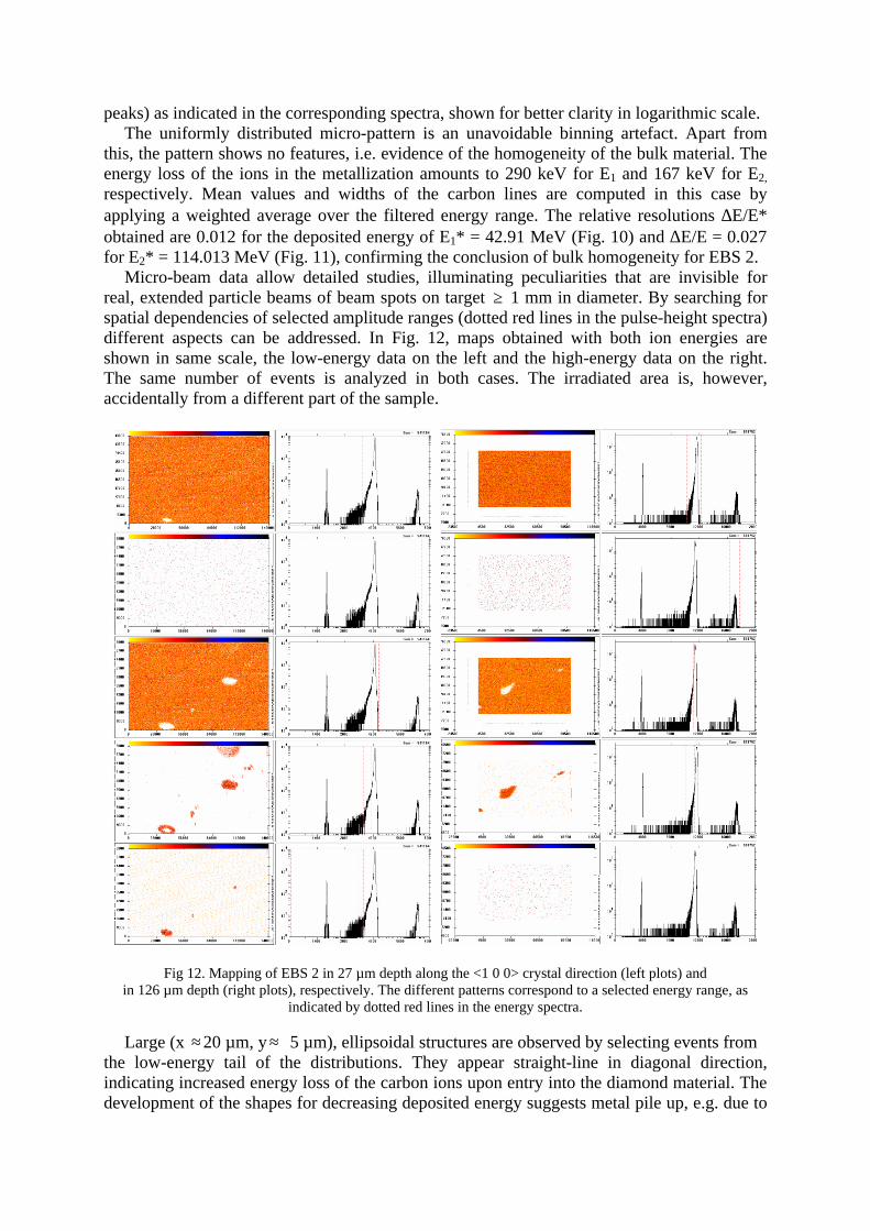
respectively. Mean values and widths of the carbon lines are computed in this case by applying a weighted average over the filtered energy range. The relative resolutions ∆E/E* obtained are 0.012 for the deposited energy of E1* = 42.91 MeV (Fig. 10) and ∆E/E = 0.027 for E2* = 114.013 MeV (Fig. 11), confirming the conclusion of bulk homogeneity for EBS 2. Micro-beam data allow detailed studies, illuminating peculiarities that are invisible for real, extended particle beams of beam spots on target ≥ 1 mm in diameter. By searching for spatial dependencies of selected amplitude ranges (dotted red lines in the pulse-height spectra) different aspects can be addressed. In Fig. 12, maps obtained with both ion energies are shown in same scale, the low-energy data on the left and the high-energy data on the right. The same number of events is analyzed in both cases. The irradiated area is, however, accidentally from a different part of the sample.
Fig 12. Mapping of EBS 2 in 27 µm depth along the <1 0 0> crystal direction (left plots) and in 126 µm depth (right plots), respectively. The different patterns correspond to a selected energy range, as
indicated by dotted red lines in the energy spectra.
Large (x ≈ 20 µm, y ≈ 5 µm), ellipsoidal structures are observed by selecting events from the low-energy tail of the distributions. They appear straight-line in diagonal direction, indicating increased energy loss of the carbon ions upon entry into the diamond material. The development of the shapes for decreasing deposited energy suggests metal pile up, e.g. due to
scratch marks. The circular structure observable at the top edge of the map in the low-energy run may be a liquid dropped on the surface during sample preparation. More interesting are two thin lines observed in 126 µm depth. Similar figures are obtained by X-ray white-beam topography in case of stress in the material.
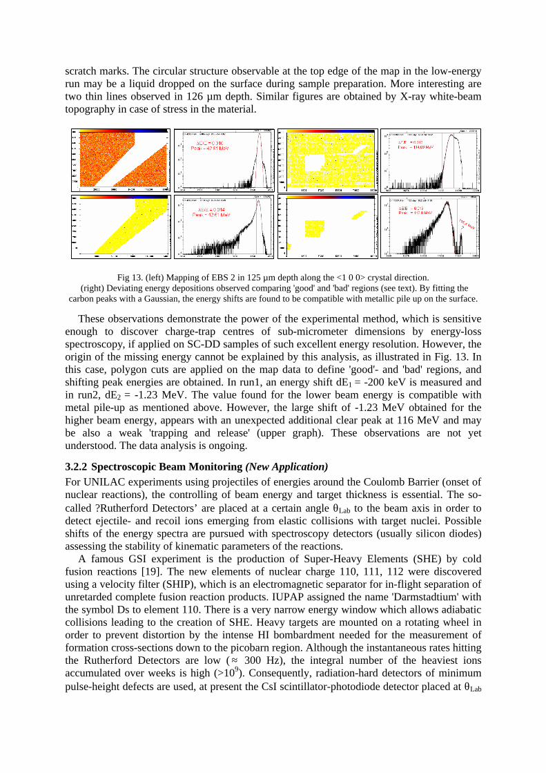
Fig 13. (left) Mapping of EBS 2 in 125 µm depth along the <1 0 0> crystal direction. (right) Deviating energy depositions observed comparing 'good' and 'bad' regions (see text). By fitting the
carbon peaks with a Gaussian, the energy shifts are found to be compatible with metallic pile up on the surface.
These observations demonstrate the power of the experimental method, which is sensitive enough to discover charge-trap centres of sub-micrometer dimensions by energy-loss spectroscopy, if applied on SC-DD samples of such excellent energy resolution. However, the origin of the missing energy cannot be explained by this analysis, as illustrated in Fig. 13. In this case, polygon cuts are applied on the map data to define 'good'- and 'bad' regions, and shifting peak energies are obtained. In run1, an energy shift dE1 = -200 keV is measured and in run2, dE2 = -1.23 MeV. The value found for the lower beam energy is compatible with metal pile-up as mentioned above. However, the large shift of -1.23 MeV obtained for the higher beam energy, appears with an unexpected additional clear peak at 116 MeV and may be also a weak 'trapping and release' (upper graph). These observations are not yet understood. The data analysis is ongoing.
3.2.2 Spectroscopic Beam Monitoring (New Application) For UNILAC experiments using projectiles of energies around the Coulomb Barrier (onset of nuclear reactions), the controlling of beam energy and target thickness is essential. The so-called ?Rutherford Detectors’ are placed at a certain angle θLab to the beam axis in order to detect ejectile- and recoil ions emerging from elastic collisions with target nuclei. Possible shifts of the energy spectra are pursued with spectroscopy detectors (usually silicon diodes) assessing the stability of kinematic parameters of the reactions. A famous GSI experiment is the production of Super-Heavy Elements (SHE) by cold fusion reactions [19]. The new elements of nuclear charge 110, 111, 112 were discovered using a velocity filter (SHIP), which is an electromagnetic separator for in-flight separation of unretarded complete fusion reaction products. IUPAP assigned the name 'Darmstadtium' with the symbol Ds to element 110. There is a very narrow energy window which allows adiabatic collisions leading to the creation of SHE. Heavy targets are mounted on a rotating wheel in order to prevent distortion by the intense HI bombardment needed for the measurement of formation cross-sections down to the picobarn region. Although the instantaneous rates hitting the Rutherford Detectors are low ( ≈ 300 Hz), the integral number of the heaviest ions accumulated over weeks is high (>109). Consequently, radiation-hard detectors of minimum pulse-height defects are used, at present the CsI scintillator-photodiode detector placed at θLab
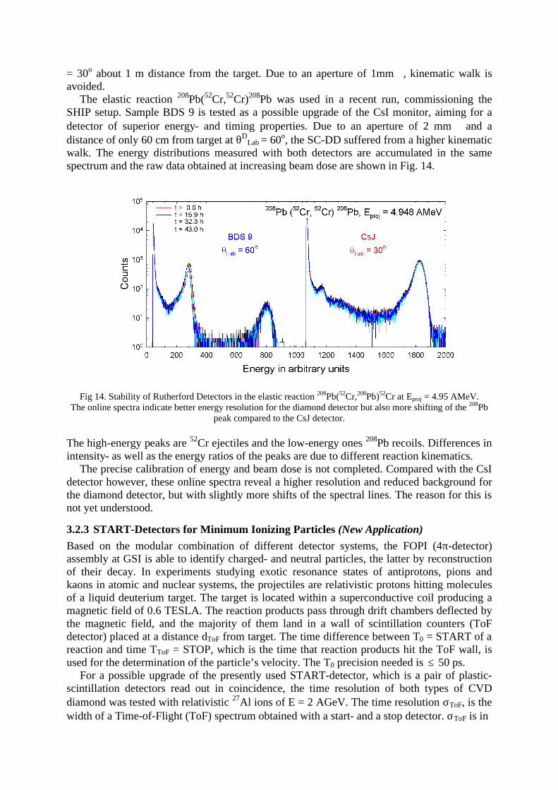
= 30o about 1 m distance from the target. Due to an aperture of 1mm∅, kinematic walk is avoided. The elastic reaction 208Pb(52Cr,52Cr)208Pb was used in a recent run, commissioning the SHIP setup. Sample BDS 9 is tested as a possible upgrade of the CsI monitor, aiming for a detector of superior energy- and timing properties. Due to an aperture of 2 mm∅ and a distance of only 60 cm from target at θD
Lab = 60o, the SC-DD suffered from a higher kinematic walk. The energy distributions measured with both detectors are accumulated in the same spectrum and the raw data obtained at increasing beam dose are shown in Fig. 14.
Fig 14. Stability of Rutherford Detectors in the elastic reaction 208Pb(52Cr,208Pb)52Cr at Eproj = 4.95 AMeV. The online spectra indicate better energy resolution for the diamond detector but also more shifting of the 208Pb
peak compared to the CsJ detector. The high-energy peaks are 52Cr ejectiles and the low-energy ones 208Pb recoils. Differences in intensity- as well as the energy ratios of the peaks are due to different reaction kinematics. The precise calibration of energy and beam dose is not completed. Compared with the CsI detector however, these online spectra reveal a higher resolution and reduced background for the diamond detector, but with slightly more shifts of the spectral lines. The reason for this is not yet understood.
3.2.3 START-Detectors for Minimum Ionizing Particles (New Application) Based on the modular combination of different detector systems, the FOPI (4π-detector) assembly at GSI is able to identify charged- and neutral particles, the latter by reconstruction of their decay. In experiments studying exotic resonance states of antiprotons, pions and kaons in atomic and nuclear systems, the projectiles are relativistic protons hitting molecules of a liquid deuterium target. The target is located within a superconductive coil producing a magnetic field of 0.6 TESLA. The reaction products pass through drift chambers deflected by the magnetic field, and the majority of them land in a wall of scintillation counters (ToF detector) placed at a distance dToF from target. The time difference between T0 = START of a reaction and time TToF = STOP, which is the time that reaction products hit the ToF wall, is used for the determination of the particle’s velocity. The T0 precision needed is ≤ 50 ps. For a possible upgrade of the presently used START-detector, which is a pair of plastic-scintillation detectors read out in coincidence, the time resolution of both types of CVD diamond was tested with relativistic 27Al ions of E = 2 AGeV. The time resolution σToF, is the width of a Time-of-Flight (ToF) spectrum obtained with a start- and a stop detector. σToF is in
an ideal case a δ-function convoluted with flight time tToF. In praxis however, it is affected by the intrinsic time resolution σintr of the detectors (determined with dToF = 0), by 'time-walk' σw due to error in the amplitude spread, as well as by 'time jitter' σt, which is the error due to electronic noise σN and the finite signal slope dV/dt at the discriminator threshold (|thr). σw can be compensated for knowledge of the amplitude distribution, and σt by minimizing σN at highest possible dV/dt|thr . σToF is described by relation (3)
thrdtdV
ss N
ToF= (3)
with σN depicting the electronic noise, and dV/dt|thr the signal slope at discriminator threshold.
Special ToF-FE electronics as developed for the FOPI upgrade was used to test the intrinsic resolution of 500µm thick DG-PC samples and of SC samples BDS 5 and BDS 7, each of 330µm thickness. The broadband-amplified pulses were discriminated by leading-edge triggers placed in the cave near the detectors, and the resulting digital pulses were transferred over 30 m long transmission lines to the electronic setup and to the data-acquisition system.
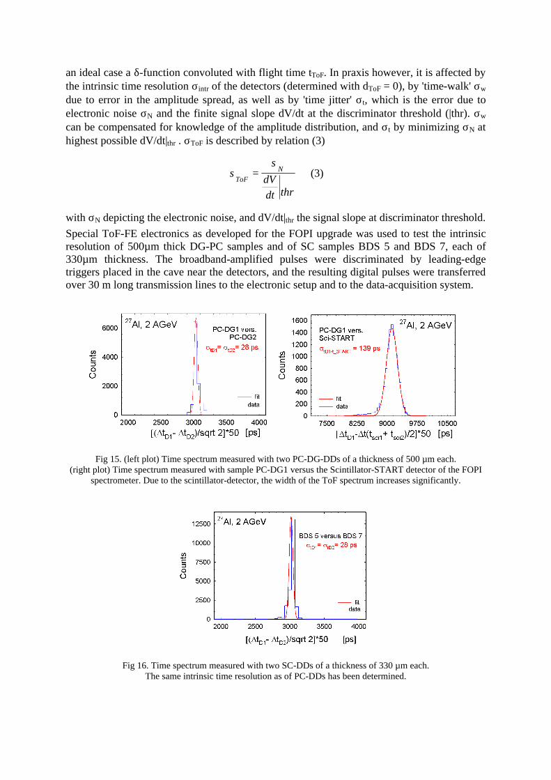
Fig 15. (left plot) Time spectrum measured with two PC-DG-DDs of a thickness of 500 µm each. (right plot) Time spectrum measured with sample PC-DG1 versus the Scintillator-START detector of the FOPI
spectrometer. Due to the scintillator-detector, the width of the ToF spectrum increases significantly.
Fig 16. Time spectrum measured with two SC-DDs of a thickness of 330 µm each. The same intrinsic time resolution as of PC-DDs has been determined.
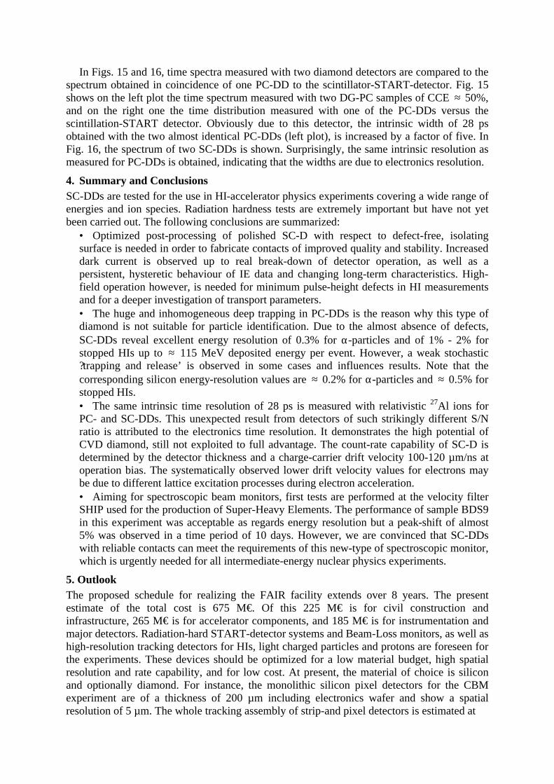
In Figs. 15 and 16, time spectra measured with two diamond detectors are compared to the spectrum obtained in coincidence of one PC-DD to the scintillator-START-detector. Fig. 15 shows on the left plot the time spectrum measured with two DG-PC samples of CCE ≈ 50%, and on the right one the time distribution measured with one of the PC-DDs versus the scintillation-START detector. Obviously due to this detector, the intrinsic width of 28 ps obtained with the two almost identical PC-DDs (left plot), is increased by a factor of five. In Fig. 16, the spectrum of two SC-DDs is shown. Surprisingly, the same intrinsic resolution as measured for PC-DDs is obtained, indicating that the widths are due to electronics resolution.
4. Summary and Conclusions SC-DDs are tested for the use in HI-accelerator physics experiments covering a wide range of energies and ion species. Radiation hardness tests are extremely important but have not yet been carried out. The following conclusions are summarized:
• Optimized post-processing of polished SC-D with respect to defect-free, isolating surface is needed in order to fabricate contacts of improved quality and stability. Increased dark current is observed up to real break-down of detector operation, as well as a persistent, hysteretic behaviour of IE data and changing long-term characteristics. High-field operation however, is needed for minimum pulse-height defects in HI measurements and for a deeper investigation of transport parameters. • The huge and inhomogeneous deep trapping in PC-DDs is the reason why this type of diamond is not suitable for particle identification. Due to the almost absence of defects, SC-DDs reveal excellent energy resolution of 0.3% for α-particles and of 1% - 2% for stopped HIs up to ≈ 115 MeV deposited energy per event. However, a weak stochastic ?trapping and release’ is observed in some cases and influences results. Note that the corresponding silicon energy-resolution values are ≈ 0.2% for α-particles and ≈ 0.5% for stopped HIs. • The same intrinsic time resolution of 28 ps is measured with relativistic 27Al ions for PC- and SC-DDs. This unexpected result from detectors of such strikingly different S/N ratio is attributed to the electronics time resolution. It demonstrates the high potential of CVD diamond, still not exploited to full advantage. The count-rate capability of SC-D is determined by the detector thickness and a charge-carrier drift velocity 100-120 µm/ns at operation bias. The systematically observed lower drift velocity values for electrons may be due to different lattice excitation processes during electron acceleration. • Aiming for spectroscopic beam monitors, first tests are performed at the velocity filter SHIP used for the production of Super-Heavy Elements. The performance of sample BDS9 in this experiment was acceptable as regards energy resolution but a peak-shift of almost 5% was observed in a time period of 10 days. However, we are convinced that SC-DDs with reliable contacts can meet the requirements of this new-type of spectroscopic monitor, which is urgently needed for all intermediate-energy nuclear physics experiments.
5. Outlook The proposed schedule for realizing the FAIR facility extends over 8 years. The present estimate of the total cost is 675 M€. Of this 225 M€ is for civil construction and infrastructure, 265 M€ is for accelerator components, and 185 M€ is for instrumentation and major detectors. Radiation-hard START-detector systems and Beam-Loss monitors, as well as high-resolution tracking detectors for HIs, light charged particles and protons are foreseen for the experiments. These devices should be optimized for a low material budget, high spatial resolution and rate capability, and for low cost. At present, the material of choice is silicon and optionally diamond. For instance, the monolithic silicon pixel detectors for the CBM experiment are of a thickness of 200 µm including electronics wafer and show a spatial resolution of 5 µm. The whole tracking assembly of strip-and pixel detectors is estimated at
10 M€ for a total area of 1.8 square meters. The convincing CVDD results obtained at GSI show that this material is competing more and more with silicon detectors, unsuitable as regards radiation hardness and rate capability. PC-D is expected to fit the needs of HI tracking devices in all cases where particle identification is not required, and SC-D those of vertex detectors for MIPs. However, in order to consider diamond, larger and thinner wafers of a thickness well below 300 µm must be available, and – last but not least - the material costs must decrease significantly.
Acknowledgment This work is supported by the EC, Project RII3-CT-2004-506078. We express our gratitude to Element Six, Ascot UK for the generous provision of early SC CVD-diamond samples. We acknowledge the ID21 and ID29 beamlines at the ESRF Grenoble for access to synchrotron radiation, the GSI's Target Laboratory crew for the samples metallization and all colleagues contributing steadily increasing interest and new ideas for the use of CVD-diamond detectors.
References [1] E. Berdermann, K. Blasche, P. Moritz, H.Stelzer, F. Zeytouni, Diamond Detectors for Heavy Ion Measurements, Proc. of the XXXVI International Winter Meeting on Nuclear Physics, p.589-603, Edt. by I. Iori, Bormio Italy, 1998 [2] E. Berdermann, K. Blasche, P. Moritz, H. Stelzer, B. Voss, F. Zeytouni, First Applications of CVD-Diamond Detectors in Heavy-Ion Experiments, 6th International Conference on Advanced Technology and Particle Physics (ICATPP-6), Como Italy, October 1998, Nuclear Physics B (Proc. Suppl.) 78 (1999) 533-539 [3] E. Berdermann, K. Blasche, P. Moritz, H. Stelzer, B. Voss, The Use of CVD-Diamond for Heavy-Ion
Detection, Proc. of the 7th International Conference on New Diamond Science&Technology (ICNDST-7), Hong-Kong 2000, Diamond and Related Materials 10 (2001) 1770-1777
[4] E. Berdermann, K. Blasche, H. W. Daues, P. Moritz, H. Stelzer, B. Voss, The Diamond Project at GSI – Perspectives, Proc. of the 7th International Conference on Advanced Technology and Particle Physics (ICATPP-7), Como Italy, October 2001, p. 246-251, World Scientific [5] J. Bol, E. Berdermann, W. deBoer, E. Grigoriev, F. Hauler, and L. Jungermann, Beam Monitors for TESLA based on Diamond Strip Detectors, IEEE Transactions on Nuclear Science, Vol. 51, No. 6, December 2004 [6] M. Rebisz, A. Martemiyanov, E. Berdermann, M. Pomorski, B. Marczewska, and B. Voss, Synthetic Diamonds for Heavy-Ion Therapy Dosimetry, Proc. of the Diamond 2005, Toulouse, to be published [7] G. Kraft, Nucl. Instr. and Meth. in Phys. Res. A 454 (2000) 1-10 [8] C.M. Buttar, R. Airey, J. Conway, G. Hill, S. Ramkumar, G.Scarsbrook, R.S. Sussmann, S. Walker, A. Whitehead, Diamond Relat. Mater. 9 (2000) 965-969 [9] C. Nebel, Optische und Elektronische Eigenschaften von CVD Diamant, Habilitationsschrift, Technical University of Munich, 1998 [10] Dirk Meier, CVD Diamond Sensors for Particle Detection and Tracking, PhD Thesis, University of Heidelberg, 1999 [11] P. Moritz, E. Berdermann, K. Blasche, H. Stelzer, B. Voss, Broadband electronics for Diamond Detectors,
Proc. of the 7th International Conference on New Diamond Science&Technology (ICNDST-7), Hong-Kong 2000, Diamond and Related Materials 10 (2001) 1770-1777 [12] C. Jacoboni et al., Solid State Electronics 20 (1977) 77 [13] H. Pernegger, S. Roe, P.Weilhammer, V. Eremin, H. Frais-Kölbl, E. Griesmayer, H. Kagan, S. Schnetzer, R. Stone, W. Trischuk, D. Twitchen, A. Whitehead, Journal of Applied Physics 97, 073704 (2005) [14] M. Pomorski, E. Berdermann, M. Ciobanu, A. Martemiyanov, P. Moritz, M. Rebisz, B. Marczewska, phys. stat. sol. (a) 202, No. 11 (2005) [15] E. Berdermann for the NoRHDia Collaboration, Proc. of the XLIII Intern. Winter Meetingon Nuclear Physics, p. 371-381, Edt. by I. Iori and A. Bortolotti, Bormio Italy, 2005 [16] J. Isberg et al., Science 297 (2002) [17] Fo et al., CSTA2 TU Darmstadt [18] EG&G Ortec, "Modular Pulse-Processing Electronics and Semiconductor Radiation Detectors", #95, (1994) [19] S. Hofmann and G. Münzenberg, The Discovery of the Heaviest Elements, Rev. Mod. Phys., 72, 733-767, 2000; more in http://www.gsi.de/forschung/kp/kp2/ship/education/edu.html