Embed Size (px)
Citation preview
IEEE TRANSACTIONS ON NUCLEAR SCIENCE, VOL. 60, NO. 4, AUGUST 2013 2623
Radiation Effects in CMOS Isolation Oxides:Differences and Similarities With Thermal Oxides
Marc Gaillardin, Member, IEEE, Vincent Goiffon, Member, IEEE, Claude Marcandella,Sylvain Girard, Senior Member, IEEE, Martial Martinez, Philippe Paillet, Senior Member, IEEE,
Pierre Magnan, Member, IEEE, and Magali Estribeau, Member, IEEE
Abstract—Radiation effects in thick isolation oxides of modernCMOS technologies are investigated using dedicated test struc-tures designed using two commercial foundries. Shallow TrenchIsolation and Pre-Metal Dielectric are studied using electricalmeasurements performed after X-ray irradiations and isochronalannealing cycles. This paper shows that trapping properties ofsuch isolation oxides can strongly differ from those of tradi-tional thermal oxides usually used to process the gate oxide ofMetal Oxide Semiconductor Field Effect Transistors. Buildupand annealing of both radiation-induced oxide-trap charge andradiation-induced interface traps are discussed as a function ofthe oxide type, foundry and bias condition during irradiation. Ra-diation-induced interface traps in such isolation oxides are shownto anneal below contrary to what is usually observed inthermal oxides. Implications for design hardening and radiationtests of CMOS Integrated Circuits are discussed.
Index Terms—CMOS, CMOS image sensors (CIS), pre-metal di-electric (PMD), shallow trench isolation (STI), total ionizing dose(TID), transistors.
I. INTRODUCTION
T HE generation of charges by ionizing radiations inCMOS materials may induce stable defects in dielectrics
[1] used in the fabrication process. This phenomenon results inmodifications of CMOS devices electrical characteristics, suchas threshold voltage shifts in MOSFETs, or intense leakagecurrents. Since the number of defects generated in gate-oxidereduces with its thickness, this effect becomes negligible inmodern Integrated Circuits (ICs). Total Ionizing Dose (TID)induced degradation of modern CMOS integrated circuits isthus now governed by field or isolation oxides such as ShallowTrench Isolation (STI) [2], [3] or Pre-Metal Dielectric (PMD).They are deposited oxides contrary to the widely studiedgate-oxide which is thermally grown. Unlike thermally grownoxides, few data are available on trapping properties andinterface trap buildup rate of these deposited oxides [4]–[9].
Manuscript received September 28, 2012; revised January 16, 2013; acceptedFebruary 20, 2013. Date of publication April 05, 2013; date of current versionAugust 14, 2013.M. Gaillardin, C. Marcandella, M. Martinez, and P. Paillet are with the CEA,
DAM, DIF, F-91297 Arpajon, France (e-mail: [email protected]; [email protected]; [email protected]; [email protected]).S. Girard is with the Laboratoire H. Curien, UMR CNRS 5516, Université
Jean Monnet, 42000, Saint-Etienne, France (e-mail: [email protected]).V. Goiffon, P. Magnan, and M. Estribeau are with the ISAE, Université
de Toulouse, BP 54032, 31055 Toulouse Cedex 4, France (e-mail: [email protected]; [email protected]; [email protected]).Color versions of one or more of the figures in this paper are available online
at http://ieeexplore.ieee.org.Digital Object Identifier 10.1109/TNS.2013.2249094
Most studies on deposited oxides focus on electrical effects inICs due to trapping in STIs [10]–[13]. A complete analysis ofphysical mechanisms occurring in deposited oxides—STI butalso PMD [14]—under ionizing radiation and after annealingremains needed. This will help foreseeing the behavior offuture technologies designed for specific applications whichare very sensitive to deposited oxide such as analog devices,bipolar technologies [15], [16], DRAMs, or CMOS image sen-sors [17]–[19]. In this paper, we investigate the defect densityevolution of two types of thick deposited oxides submitted toTotal Ionizing Dose (TID) using dedicated custom test struc-tures processed in two deep submicron commercially availabletechnologies. This paper is especially focused on the ionizingradiation behavior of grounded deposited oxides which play animportant role in the radiation response of several CMOS ICs.For instance, in CMOS Image Sensors (CIS) the most sensitivenode is the photodiode which is surrounded by a groundeddeposited oxide (STI or PMD). However, it may also be criticalin circuits where the leakage current of any PN junction ina CMOS ICs is an issue. So, knowing the behavior of thickisolation oxides grounded during irradiation will help one toimprove hardening level of CMOS ICs.
II. EXPERIMENTAL DETAILS
A. Test Structures
Specific devices were fabricated using two commercial bulkm processes. They consist in large nMOS transistors
which gate oxide is made of either a STI Fig. 1(a) or a PMDFig. 1(b), both being deposited oxides. In the following, theyare referred to as STIFET and PMDFET respectively. In bothdevices the Pwell-doped region is located under the thick “gateoxide” and between two Nwell-doped regions which act assource and drain. The gate is either made of standard polysiliconor of the first metal layer from the back end of line. The exactdetails of the process are not described in this paper. However,usual STI process flows involve a thin thermally grown linerfollowed by the STI deposition before planarization. Thethermal liner is about 30 nm thick and the total STI stack thick-ness is about 400 nm [20]. The PMD follows several processsteps after the STI creation: gate oxide growth, gate polysilicondeposition, gate lithography and Reactive Ion Etching (RIE)of the entire wafer before PMD deposition [20]. This way, thegate oxide is removed on the entire wafer, except under thegate electrode. There is no “high quality” oxide between thePMD, usually deposited in two steps, and the active silicon.The complete PMD-stack is about 550 nm-thick. Since we do
0018-9499 © 2013 IEEE
2624 IEEE TRANSACTIONS ON NUCLEAR SCIENCE, VOL. 60, NO. 4, AUGUST 2013
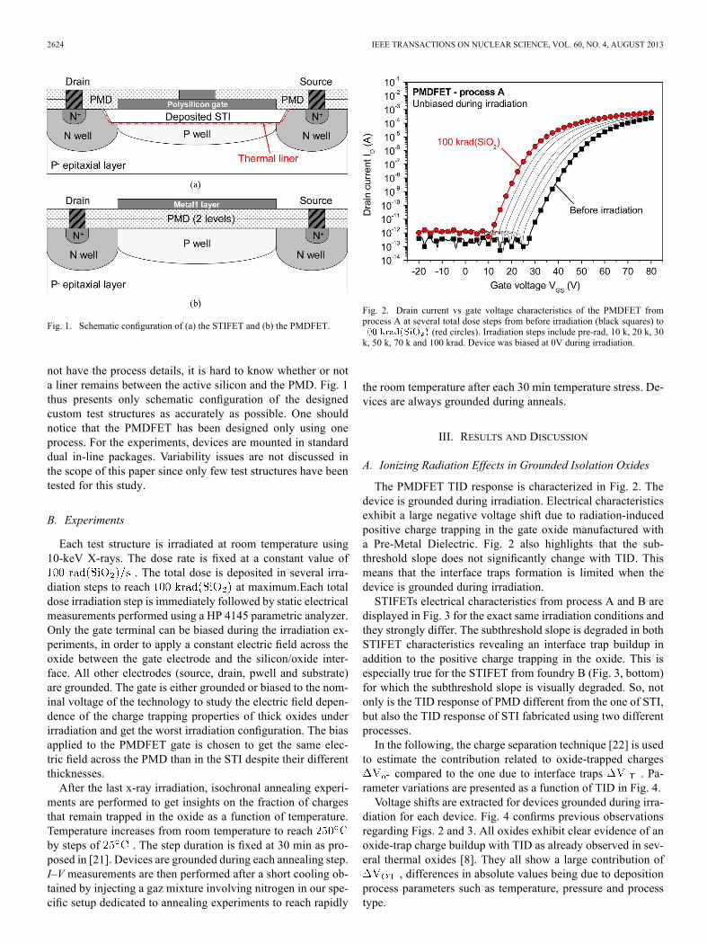
Fig. 1. Schematic configuration of (a) the STIFET and (b) the PMDFET.
not have the process details, it is hard to know whether or nota liner remains between the active silicon and the PMD. Fig. 1thus presents only schematic configuration of the designedcustom test structures as accurately as possible. One shouldnotice that the PMDFET has been designed only using oneprocess. For the experiments, devices are mounted in standarddual in-line packages. Variability issues are not discussed inthe scope of this paper since only few test structures have beentested for this study.
B. Experiments
Each test structure is irradiated at room temperature using10-keV X-rays. The dose rate is fixed at a constant value of
. The total dose is deposited in several irra-diation steps to reach at maximum.Each totaldose irradiation step is immediately followed by static electricalmeasurements performed using a HP 4145 parametric analyzer.Only the gate terminal can be biased during the irradiation ex-periments, in order to apply a constant electric field across theoxide between the gate electrode and the silicon/oxide inter-face. All other electrodes (source, drain, pwell and substrate)are grounded. The gate is either grounded or biased to the nom-inal voltage of the technology to study the electric field depen-dence of the charge trapping properties of thick oxides underirradiation and get the worst irradiation configuration. The biasapplied to the PMDFET gate is chosen to get the same elec-tric field across the PMD than in the STI despite their differentthicknesses.After the last x-ray irradiation, isochronal annealing experi-
ments are performed to get insights on the fraction of chargesthat remain trapped in the oxide as a function of temperature.Temperature increases from room temperature to reachby steps of . The step duration is fixed at 30 min as pro-posed in [21]. Devices are grounded during each annealing step.I–V measurements are then performed after a short cooling ob-tained by injecting a gaz mixture involving nitrogen in our spe-cific setup dedicated to annealing experiments to reach rapidly
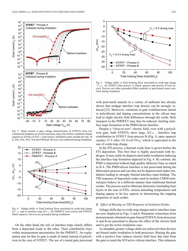
Fig. 2. Drain current vs gate voltage characteristics of the PMDFET fromprocess A at several total dose steps from before irradiation (black squares) to
(red circles). Irradiation steps include pre-rad, 10 k, 20 k, 30k, 50 k, 70 k and 100 krad. Device was biased at 0V during irradiation.
the room temperature after each 30 min temperature stress. De-vices are always grounded during anneals.
III. RESULTS AND DISCUSSION
A. Ionizing Radiation Effects in Grounded Isolation Oxides
The PMDFET TID response is characterized in Fig. 2. Thedevice is grounded during irradiation. Electrical characteristicsexhibit a large negative voltage shift due to radiation-inducedpositive charge trapping in the gate oxide manufactured witha Pre-Metal Dielectric. Fig. 2 also highlights that the sub-threshold slope does not significantly change with TID. Thismeans that the interface traps formation is limited when thedevice is grounded during irradiation.STIFETs electrical characteristics from process A and B are
displayed in Fig. 3 for the exact same irradiation conditions andthey strongly differ. The subthreshold slope is degraded in bothSTIFET characteristics revealing an interface trap buildup inaddition to the positive charge trapping in the oxide. This isespecially true for the STIFET from foundry B (Fig. 3, bottom)for which the subthreshold slope is visually degraded. So, notonly is the TID response of PMD different from the one of STI,but also the TID response of STI fabricated using two differentprocesses.In the following, the charge separation technique [22] is used
to estimate the contribution related to oxide-trapped chargescompared to the one due to interface traps . Pa-
rameter variations are presented as a function of TID in Fig. 4.Voltage shifts are extracted for devices grounded during irra-
diation for each device. Fig. 4 confirms previous observationsregarding Figs. 2 and 3. All oxides exhibit clear evidence of anoxide-trap charge buildup with TID as already observed in sev-eral thermal oxides [8]. They all show a large contribution of
, differences in absolute values being due to depositionprocess parameters such as temperature, pressure and processtype.
GAILLARDIN et al.: RADIATION EFFECTS IN CMOS ISOLATION OXIDES 2625
Fig. 3. Drain current vs gate voltage characteristics of STIFETs from twocommercial foundries at several total dose steps from before irradiation (blacksquares) to (red circles). Irradiation steps include pre-rad, 10k, 20 k, 30 k, 50 k, 70 k and 100 krad. Devices were unbiased during irradiation.
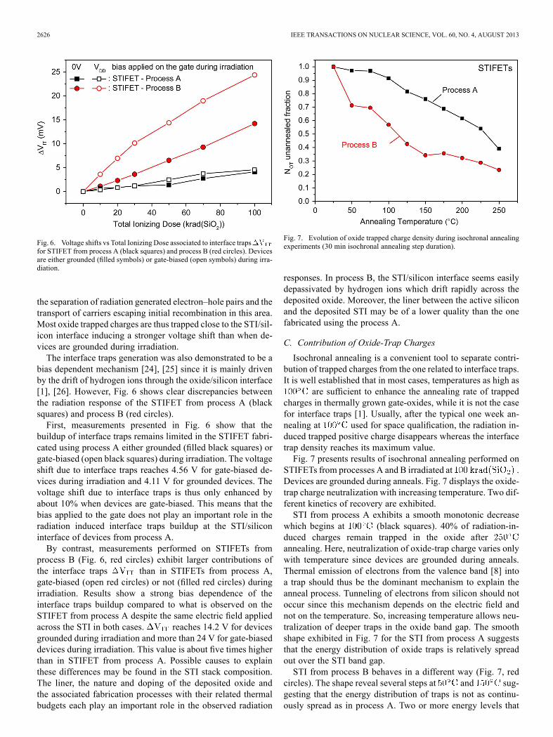
Fig. 4. Voltage shifts vs Total Ionizing Dose associated to oxide-trap chargeand to interface traps for PMDFET (red circles) and STIFETs
(black squares). Devices are grounded during irradiation.
On the other hand, the role of interface traps clearly differsfrom a deposited oxide to the other. Their contribution stayswithin measurement uncertainties for the PMDFET. An expla-nation may be that its gate is made of metal instead of polysil-icon in the case of STIFET. The use of a metal gate processed
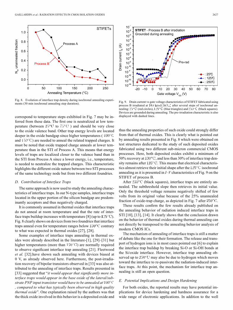
Fig. 5. Voltage shifts vs Total Ionizing Dose associated to oxide-trap chargefor STIFET from process A (black squares) and process B (red cir-
cles). Devices are either grounded (filled symbols) or gate-biased (open sym-bols) during irradiation.
with post-metal anneals in a variety of ambients has alreadyshown that midgap interface trap density can be strongly re-duced [23]. Moreover, variations in gate workfunctions (metalor polysilicon) and doping concentrations in the silicon maylead to slight electric field differences through the oxide. Holetransport in the PMDFET may thus be reduced, limiting inter-face traps formation at the PMD/silicon interface.Despite a “close-to-zero” electric field, even with a polysil-
icon gate, both STIFETs show large . Interface trapcontribution in STIFET from process B (Fig. 4, open squares)reaches 15 V after which is equivalent to theone of oxide-trap charge.In the STI process, a thermal oxide liner is grown before the
STI deposition. This first liner is highly passivated with hy-drogen. It may easily be depassivated under irradiation inducingthe interface trap formation depicted in Fig. 4. By contrast, thePMD is deposited without high quality dielectric liner as statedin II.A. The PMD/silicon interface is not passivated during thefabrication process and can thus not be depassivated under irra-diation leading to strongly limited interface traps buildup. TheTID response of deposited oxides used in modern CMOS tech-nologies behave in a different manner than traditional thermaloxides. The process used to fabricate dielectrics (including linerlayers in the case of STI), various annealing temperatures anddoping appear to be key aspects in determining the trappingproperties of such oxides.
B. Effect of Biasing on TID Response of Isolation Oxides
Voltage shifts due to oxide-trap charges and to interface trapsare now displayed in Figs. 5 and 6. Parameter extractions frommeasurements obtained on gate-biased STIFETs from processesA and B are presented to discuss the effect of the electric fieldand to get the worst irradiation case.As intended, greater voltage shifts are achieved when devices
are biased under irradiation in both processes. Biasing the gatewith a positive bias induces electric field lines that start fromthe gate to reach the STI/active silicon interface. This enhances
2626 IEEE TRANSACTIONS ON NUCLEAR SCIENCE, VOL. 60, NO. 4, AUGUST 2013
Fig. 6. Voltage shifts vs Total IonizingDose associated to interface trapsfor STIFET from process A (black squares) and process B (red circles). Devicesare either grounded (filled symbols) or gate-biased (open symbols) during irra-diation.
the separation of radiation generated electron–hole pairs and thetransport of carriers escaping initial recombination in this area.Most oxide trapped charges are thus trapped close to the STI/sil-icon interface inducing a stronger voltage shift than when de-vices are grounded during irradiation.The interface traps generation was also demonstrated to be a
bias dependent mechanism [24], [25] since it is mainly drivenby the drift of hydrogen ions through the oxide/silicon interface[1], [26]. However, Fig. 6 shows clear discrepancies betweenthe radiation response of the STIFET from process A (blacksquares) and process B (red circles).First, measurements presented in Fig. 6 show that the
buildup of interface traps remains limited in the STIFET fabri-cated using process A either grounded (filled black squares) orgate-biased (open black squares) during irradiation. The voltageshift due to interface traps reaches 4.56 V for gate-biased de-vices during irradiation and 4.11 V for grounded devices. Thevoltage shift due to interface traps is thus only enhanced byabout 10% when devices are gate-biased. This means that thebias applied to the gate does not play an important role in theradiation induced interface traps buildup at the STI/siliconinterface of devices from process A.By contrast, measurements performed on STIFETs from
process B (Fig. 6, red circles) exhibit larger contributions ofthe interface traps than in STIFETs from process A,gate-biased (open red circles) or not (filled red circles) duringirradiation. Results show a strong bias dependence of theinterface traps buildup compared to what is observed on theSTIFET from process A despite the same electric field appliedacross the STI in both cases. reaches 14.2 V for devicesgrounded during irradiation and more than 24 V for gate-biaseddevices during irradiation. This value is about five times higherthan in STIFET from process A. Possible causes to explainthese differences may be found in the STI stack composition.The liner, the nature and doping of the deposited oxide andthe associated fabrication processes with their related thermalbudgets each play an important role in the observed radiation
Fig. 7. Evolution of oxide trapped charge density during isochronal annealingexperiments (30 min isochronal annealing step duration).
responses. In process B, the STI/silicon interface seems easilydepassivated by hydrogen ions which drift rapidly across thedeposited oxide. Moreover, the liner between the active siliconand the deposited STI may be of a lower quality than the onefabricated using the process A.
C. Contribution of Oxide-Trap Charges
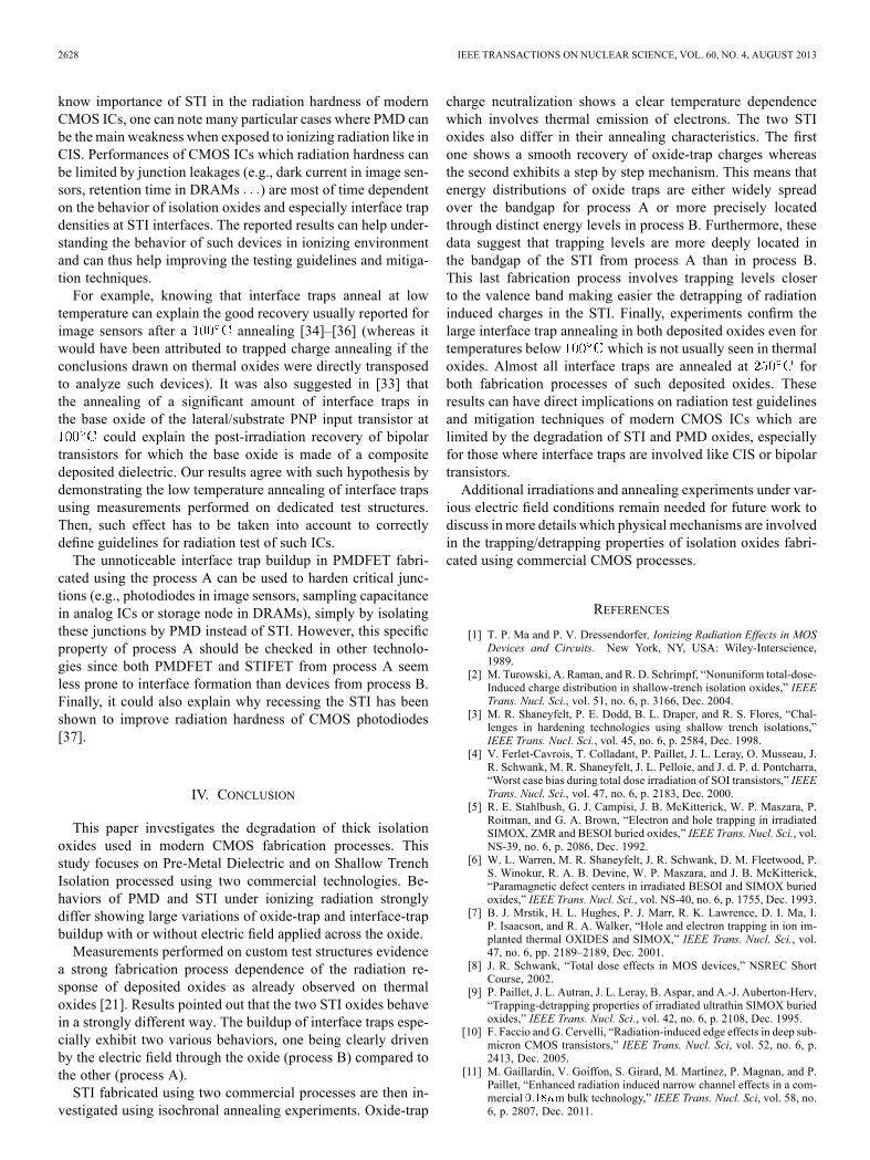
Isochronal annealing is a convenient tool to separate contri-bution of trapped charges from the one related to interface traps.It is well established that in most cases, temperatures as high as
are sufficient to enhance the annealing rate of trappedcharges in thermally grown gate-oxides, while it is not the casefor interface traps [1]. Usually, after the typical one week an-nealing at used for space qualification, the radiation in-duced trapped positive charge disappears whereas the interfacetrap density reaches its maximum value.Fig. 7 presents results of isochronal annealing performed on
STIFETs from processes A and B irradiated at .Devices are grounded during anneals. Fig. 7 displays the oxide-trap charge neutralization with increasing temperature. Two dif-ferent kinetics of recovery are exhibited.STI from process A exhibits a smooth monotonic decrease
which begins at (black squares). 40% of radiation-in-duced charges remain trapped in the oxide afterannealing. Here, neutralization of oxide-trap charge varies onlywith temperature since devices are grounded during anneals.Thermal emission of electrons from the valence band [8] intoa trap should thus be the dominant mechanism to explain theanneal process. Tunneling of electrons from silicon should notoccur since this mechanism depends on the electric field andnot on the temperature. So, increasing temperature allows neu-tralization of deeper traps in the oxide band gap. The smoothshape exhibited in Fig. 7 for the STI from process A suggeststhat the energy distribution of oxide traps is relatively spreadout over the STI band gap.STI from process B behaves in a different way (Fig. 7, red
circles). The shape reveal several steps at and sug-gesting that the energy distribution of traps is not as continu-ously spread as in process A. Two or more energy levels that
GAILLARDIN et al.: RADIATION EFFECTS IN CMOS ISOLATION OXIDES 2627
Fig. 8. Evolution of interface trap density during isochronal annealing experi-ments (30 min isochronal annealing step duration).
correspond to temperature steps exhibited in Fig. 7 may be in-ferred from these data. The first one is neutralized at low tem-perature (between to ) and should be very closeto the oxide valence band. Other trap energy levels are locateddeeper in the oxide bandgap since higher temperatures (and ) are needed to anneal the related trapped charges. Itmust be noted that oxide trapped charge anneals at lower tem-perature than in the STI of Process A. This means that energylevels of traps are localized closer to the valence band than inthe STI from Process A since a lower energy, i.e., temperature,is needed to neutralize the trapped charges. This characteristichighlights the different oxide nature between two STI processesof the same technology node but from two different foundries.
D. Contribution of Interface Traps
The same approach is now used to study the annealing charac-teristics of interface traps. In our N-type samples, interface trapslocated in the upper portion of the silicon bandgap are predom-inantly acceptors and thus negatively charged.It is commonly assumed in thermal oxides that interface traps
do not anneal at room temperature and that the rate of inter-face traps buildup increases with temperature [8] (up to ).Fig. 8 clearly shows on devices from two foundries that interfacetraps anneal even for temperature ranges below contraryto what was expected in thermal oxides [27], [28].Some examples of interface traps annealing in thermal ox-
ides were already described in the literature-[1], [29]–[31] buthigher temperatures (more than ) are normally requiredto observe significant interface trap annealing [21]. Fleetwoodet al. [32].have shown such annealing with devices biased at0 V, as already observed here. Furthermore, the post-irradia-tion recovery of bipolar transistors observed in [33] was also at-tributed to the annealing of interface traps. Results presented in[33] suggested that “it would appear that significantly more in-terface traps would appear in the base oxide of the lateral/sub-strate PNP input transistor would have to be annealed at, compared to what has typically been observed in high qualitythermal oxide”. One explanation raised by the authors was thatthe thick oxide involved in this behavior is a deposited oxide and
Fig. 9. Drain current vs gate voltage characteristics of STIFET fabricated usingprocess B irradiated at after several steps of isochronal an-nealing: (red circles), (blue triangles) and (black squares).Devices are grounded during annealing. The pre-irradiation characteristic is alsodisplayed with dashed lines.
thus the annealing properties of such oxide could strongly differfrom that of thermal oxides. This is clearly what is pointed outby annealing results presented in Fig. 8 which were obtained ontest structures dedicated to the study of such deposited oxidesfabricated using two different sub-micron commercial CMOSprocesses. Here, both deposited oxides exhibit a minimum of50% recovery at , and less than 30% of interface trap den-sity remains after . This means that electrical characteris-tics almost retrieve their initial shape after the isochronalannealing as it is presented in I–V characteristics of Fig. 9 on theSTIFET of process B.After (black squares), interface traps are entirely an-
nealed. The subthreshold slope then retrieves its initial value.Only the threshold voltage remains negatively shifted of fewvolts from its original value because of the 25% unannealedfraction of oxide-trap charge, as depicted in Fig. 7 after .These results confirm the few results already published on
the annealing behavior of radiation induced interface traps inSTI [10], [13], [14]. It clearly shows that the conclusion drawnon the behavior of thermal oxides during thermal annealing cannot directly be transposed to the annealing behavior analysis ofmodern CMOS ICs.The mechanism of annealing of interface traps is still a matter
of debate like the one for their formation. The release and trans-port of hydrogen ions is in most cases pointed out [6] to explainthe interface trap buildup by breaking Si-O or Si-OH bonds atthe Si/oxide interface. However, interface trap annealing ob-served up to may also be due to hydrogen which movestoward the interface to re-passivate the radiation-induced inter-face traps. At this point, the mechanism for interface trap an-nealing is still an open question.
E. Potential Implications and Design Hardening
For both oxides, the reported results may have potential im-plications for device hardening and hardness assurance for awide range of electronic applications. In addition to the well
2628 IEEE TRANSACTIONS ON NUCLEAR SCIENCE, VOL. 60, NO. 4, AUGUST 2013
know importance of STI in the radiation hardness of modernCMOS ICs, one can note many particular cases where PMD canbe the main weakness when exposed to ionizing radiation like inCIS. Performances of CMOS ICs which radiation hardness canbe limited by junction leakages (e.g., dark current in image sen-sors, retention time in DRAMs ) are most of time dependenton the behavior of isolation oxides and especially interface trapdensities at STI interfaces. The reported results can help under-standing the behavior of such devices in ionizing environmentand can thus help improving the testing guidelines and mitiga-tion techniques.For example, knowing that interface traps anneal at low
temperature can explain the good recovery usually reported forimage sensors after a annealing [34]–[36] (whereas itwould have been attributed to trapped charge annealing if theconclusions drawn on thermal oxides were directly transposedto analyze such devices). It was also suggested in [33] thatthe annealing of a significant amount of interface traps inthe base oxide of the lateral/substrate PNP input transistor at
could explain the post-irradiation recovery of bipolartransistors for which the base oxide is made of a compositedeposited dielectric. Our results agree with such hypothesis bydemonstrating the low temperature annealing of interface trapsusing measurements performed on dedicated test structures.Then, such effect has to be taken into account to correctlydefine guidelines for radiation test of such ICs.The unnoticeable interface trap buildup in PMDFET fabri-
cated using the process A can be used to harden critical junc-tions (e.g., photodiodes in image sensors, sampling capacitancein analog ICs or storage node in DRAMs), simply by isolatingthese junctions by PMD instead of STI. However, this specificproperty of process A should be checked in other technolo-gies since both PMDFET and STIFET from process A seemless prone to interface formation than devices from process B.Finally, it could also explain why recessing the STI has beenshown to improve radiation hardness of CMOS photodiodes[37].
IV. CONCLUSION
This paper investigates the degradation of thick isolationoxides used in modern CMOS fabrication processes. Thisstudy focuses on Pre-Metal Dielectric and on Shallow TrenchIsolation processed using two commercial technologies. Be-haviors of PMD and STI under ionizing radiation stronglydiffer showing large variations of oxide-trap and interface-trapbuildup with or without electric field applied across the oxide.Measurements performed on custom test structures evidence
a strong fabrication process dependence of the radiation re-sponse of deposited oxides as already observed on thermaloxides [21]. Results pointed out that the two STI oxides behavein a strongly different way. The buildup of interface traps espe-cially exhibit two various behaviors, one being clearly drivenby the electric field through the oxide (process B) compared tothe other (process A).STI fabricated using two commercial processes are then in-
vestigated using isochronal annealing experiments. Oxide-trap
charge neutralization shows a clear temperature dependencewhich involves thermal emission of electrons. The two STIoxides also differ in their annealing characteristics. The firstone shows a smooth recovery of oxide-trap charges whereasthe second exhibits a step by step mechanism. This means thatenergy distributions of oxide traps are either widely spreadover the bandgap for process A or more precisely locatedthrough distinct energy levels in process B. Furthermore, thesedata suggest that trapping levels are more deeply located inthe bandgap of the STI from process A than in process B.This last fabrication process involves trapping levels closerto the valence band making easier the detrapping of radiationinduced charges in the STI. Finally, experiments confirm thelarge interface trap annealing in both deposited oxides even fortemperatures below which is not usually seen in thermaloxides. Almost all interface traps are annealed at forboth fabrication processes of such deposited oxides. Theseresults can have direct implications on radiation test guidelinesand mitigation techniques of modern CMOS ICs which arelimited by the degradation of STI and PMD oxides, especiallyfor those where interface traps are involved like CIS or bipolartransistors.Additional irradiations and annealing experiments under var-
ious electric field conditions remain needed for future work todiscuss in more details which physical mechanisms are involvedin the trapping/detrapping properties of isolation oxides fabri-cated using commercial CMOS processes.
REFERENCES
[1] T. P. Ma and P. V. Dressendorfer, Ionizing Radiation Effects in MOSDevices and Circuits. New York, NY, USA: Wiley-Interscience,1989.
[2] M. Turowski, A. Raman, and R. D. Schrimpf, “Nonuniform total-dose-Induced charge distribution in shallow-trench isolation oxides,” IEEETrans. Nucl. Sci., vol. 51, no. 6, p. 3166, Dec. 2004.
[3] M. R. Shaneyfelt, P. E. Dodd, B. L. Draper, and R. S. Flores, “Chal-lenges in hardening technologies using shallow trench isolations,”IEEE Trans. Nucl. Sci., vol. 45, no. 6, p. 2584, Dec. 1998.
[4] V. Ferlet-Cavrois, T. Colladant, P. Paillet, J. L. Leray, O. Musseau, J.R. Schwank, M. R. Shaneyfelt, J. L. Pelloie, and J. d. P. d. Pontcharra,“Worst case bias during total dose irradiation of SOI transistors,” IEEETrans. Nucl. Sci., vol. 47, no. 6, p. 2183, Dec. 2000.
[5] R. E. Stahlbush, G. J. Campisi, J. B. McKitterick, W. P. Maszara, P.Roitman, and G. A. Brown, “Electron and hole trapping in irradiatedSIMOX, ZMR and BESOI buried oxides,” IEEE Trans. Nucl. Sci., vol.NS-39, no. 6, p. 2086, Dec. 1992.
[6] W. L. Warren, M. R. Shaneyfelt, J. R. Schwank, D. M. Fleetwood, P.S. Winokur, R. A. B. Devine, W. P. Maszara, and J. B. McKitterick,“Paramagnetic defect centers in irradiated BESOI and SIMOX buriedoxides,” IEEE Trans. Nucl. Sci., vol. NS-40, no. 6, p. 1755, Dec. 1993.
[7] B. J. Mrstik, H. L. Hughes, P. J. Marr, R. K. Lawrence, D. I. Ma, I.P. Isaacson, and R. A. Walker, “Hole and electron trapping in ion im-planted thermal OXIDES and SIMOX,” IEEE Trans. Nucl. Sci., vol.47, no. 6, pp. 2189–2189, Dec. 2001.
[8] J. R. Schwank, “Total dose effects in MOS devices,” NSREC ShortCourse, 2002.
[9] P. Paillet, J. L. Autran, J. L. Leray, B. Aspar, and A.-J. Auberton-Herv,“Trapping-detrapping properties of irradiated ultrathin SIMOX buriedoxides,” IEEE Trans. Nucl. Sci., vol. 42, no. 6, p. 2108, Dec. 1995.
[10] F. Faccio and G. Cervelli, “Radiation-induced edge effects in deep sub-micron CMOS transistors,” IEEE Trans. Nucl. Sci, vol. 52, no. 6, p.2413, Dec. 2005.
[11] M. Gaillardin, V. Goiffon, S. Girard, M. Martinez, P. Magnan, and P.Paillet, “Enhanced radiation induced narrow channel effects in a com-mercial m bulk technology,” IEEE Trans. Nucl. Sci, vol. 58, no.6, p. 2807, Dec. 2011.
GAILLARDIN et al.: RADIATION EFFECTS IN CMOS ISOLATION OXIDES 2629
[12] C. Brisset, V. Ferlet-Cavrois, O. Flament, O. Musseau, J. L. Leray, J.L. Pelloie, R. Escoffier, A. Michez, C. Cirba, and G. Bordure, “Two-dimensional simulation of total dose effects on NMOSFET with lateralparasitic transistor,” IEEE Trans. Nucl. Sci, vol. 43, no. 6, p. 2651, Dec.1996.
[13] F. Faccio, H. J. Barnaby, X. J. Chen, D. M. Fleetwood, L. Gonella,M. McLain, and R. D. Schrimpf, “Total ionizing dose effects inshallow trench isolation oxides,” Microelectron. Reliab., vol. 48, pp.1000–1007, 2008.
[14] V. Goiffon, C. Virmontois, P. Magnan, S. Girard, and P. Paillet, “Anal-ysis of total dose-induced dark current in CMOS image sensors frominterface state and trapped charge density measurements,” IEEE Trans.Nucl. Sci., vol. 57, no. 6, p. 3087, Dec. 2010.
[15] A. H. Johnston, G. M. Swift, and B. G. Rax, “Total dose effects inconventional bipolar transistors and linear integrated circuits,” IEEETrans. Nucl. Sci., vol. 41, no. 6, p. 2427, Dec. 1994.
[16] Z. Xiao, M. Qiao, B. Zhang, and J. Xu, “Total dose characteristicsof high voltage LDMOS on SIMOX substrate,” in Proc. Int. Conf.Commun. Circuits Syst., 2007, p. 1265.
[17] G. R. Hopkinson, “Radiation effects in a CMOS active pixel sensor,”IEEE Trans. Nucl. Sci, vol. 47, no. 6, p. 2480, Dec. 2000.
[18] V. Goiffon, M. Estribeau, and P. Magnan, “Overview of ionizing ra-diation effects in image sensors fabricated in a deep-submicrometerCMOS imaging technology,” IEEE Trans. Electron. Dev., vol. 56, no.11, p. 2594, Nov. 2009.
[19] C. Virmontois, V. Goiffon, P. Magnan, O. Saint-Pe, S. Girard, S. Petit,G. Rolland, and A. Bardoux, “Total ionizing dose versus displacementdamage dose induced dark current random telegraph signals in CMOSimage sensors,” IEEE Trans. Nucl. Sci, vol. 58, no. 6, p. 3085, Dec.2011.
[20] Y. Taur and T. H. Ning, Fundamentals of modern VLSI devices ap-pendix 1: CMOS Process Flow , 2nd ed. Cambridge, U.K.: Cam-bridge Univ. Press , 2010.
[21] A. J. Lelis, T. R. Oldham, andW.M. DeLancey, “Response of interfacetraps during high-temperature anneals,” IEEE Trans. Nucl. Sci., vol. 38,no. 6, pp. 1590–1597, Dec. 1991.
[22] P. J. McWhorter and P. S. Winokur, “Simple technique for separatingthe effects of interface traps and trapped-oxide charge in metal-oxide-semiconductor transistors,” Appl. Phys. Lett., vol. 48, no. 2, p. 133,1986.
[23] M. L. Reed and J. D. Plummer, “Chemistry of Si-Si02 interface trapannealing,” J. Appl. Phys., vol. 63, p. 5776, 1988.
[24] N. S. Saks, D. B. Brown, and R. W. Rendell, “Effects of switched biason radiation-induced interface trap formation,” IEEE Trans. Nucl. Sci.,vol. 38, no. 6, pp. 1130–1139, 1991.
[25] P. S. Winokur, H. E. Boesch, Jr, J. J. M. McGarrity, and F. B. McLean,“Field- and time-dependent radiation effects at the Si/Sio2 interface ofhardened MOS capacitors,” IEEE Trans. Nucl. Sci., vol. 24, no. 6, pp.2113–2118, Dec. 1977.
[26] J. M. McGarrity, P. S. Winokur, H. E. Boesch, Jr, and F. B. McLean,“Interface states resulting from a hole flux incident on the SiO2/Si in-terface,” Phys. SiO2 Interfaces, pp. 428–432, 1978.
[27] P. L. McWhorter and W. Miller, “Modeling the anneal of radiation-induced trapped holes in varying thermal environment,” IEEE Trans.Nucl. Sci., vol. 37, no. 6, p. 1682, Dec. 1990.
[28] D. M. Fleetwood, F. V. Thome, S. S. Tsao, P. V. Dressendorfer, V.J. Dandini, and J. R. Schwank, “High-temperature silicon-on-insulatorelectronics for space nuclear power systems: Requirements and fea-sibility,” IEEE Trans. Nucl. Sci., vol. 35, no. 5, pp. 1099–1112, Oct.1988.
[29] N. S. Saks, D. B. Brown, and R. W. Rendell, “Effects of switched biason radiation-induced interface trap formation,” IEEE Trans. Nucl. Sci.,vol. 38, no. 6, p. 1130, Dec. 1991.
[30] P. S. Winokur, H. E. Boesch, Jr, J. M. McGarrity, and F. B. McLean,“Two-stage process for buildup of radiation-induced interface states,”J. Appl. Phys., vol. 50, no. 5, p. 3492, 1979.
[31] D. M. Fleetwood, P. V. Dressendorfer, and D. C. Turpin, “A reevalua-tion of the worst-case postirradiation response for hardened mos tran-sistors,” IEEE Trans. Nucl. Sci., vol. 34, no. 6, p. 1178, Dec. 1987.
[32] D. M. Fleetwood, P. V. Dressendorfer, and D. C. Turpin, “A reevalua-tion of worst-case postirradiation response for hardened MOS transis-tors,” IEEE Trans. Nucl. Sci., vol. 34, no. 6, pp. 1178–1183, Dec. 1987.
[33] M. R. Shaneyfelt, J. R. Schwank, D. M. Fleetwood, R. L. Pease, J. A.Felix, P. E. Dodd, and M. C. Maher, “Annealing behaviour of linearbipolar devices with enhanced low-dose-rate sensitivity,” IEEE Trans.Nucl. Sci., vol. 51, no. 6, pp. 3172–3177, Dec. 2004.
[34] G. R. Hopkinson, “Radiation effects in a CMOS active pixel sensor,”IEEE; Trans. Nucl. Sci., vol. 47, no. 6, pp. 2480–2484, Dec. 2000.
[35] V. Goiffon, P. Magnan, O. Saint-Pe, F. Bernard, and G. Rolland,“Total dose evaluation of deep submicron CMOS imaging technologythrough elementary device and pixel array behavior analysis,” IEEETrans. Nucl. Sci., vol. 55, no. 6, pp. 3494–3501, Dec. 2008.
[36] M. Beaumel, D. Hervé, and D. V. Aken, “Cobalt-60, proton andelectron irradiation of a radiation-hardened active pixel sensor,” IEEETrans. Nucl. Sci., vol. 57, no. 4, pp. 2056–2065, Aug. 2010.
[37] B. Pain, B. Hancock, T. J. Cunningham, S. Seshadri, C. Sun, P. Ped-dada, C. Wrigley, and R. C. Stribl, “Hardening CMOS imagers: Rad-hard-by-design jor radhard-by-foundry,” Proc. SPIE, vol. 5167, p. 101,2004.