Embed Size (px)
Citation preview
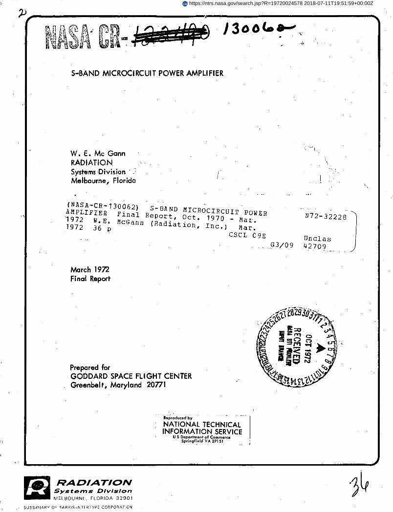
S-BAND MICROCIRCUIT POWER AMPLIFIER
W. E. Mc GannRADIAT-IONSystems Division -Melbourne, Florida
(NASA-CR- 13006 2 ) S-BIAMPLIFIER Final RepoI1972 w.E. McGann (Rad1972 36 p
AND MICROCIRCUIT PCrt, Oct. 1970 - Mardiation, Inc.) Mar
CSCL
.. I j
DWER N72-3222 8
C 9 E rUnclasG3/09 42709- .
March 1972Final Report
Prepared forGODDARD SPACE FLIGHT CENTERGreenbelt, Maryland 20771
Reproduced by
NATIONAL TECHNICALINFORMATION SERVICE
U S Department of CommerceSpringfield VA 22151
RA DI/ATIONSystems DivisionMELBOURNE, FLORIDA 32901
SUBSIDIARY OF HARRIS-INTERTYPE CORPORATION
wm-
N
:
-
https://ntrs.nasa.gov/search.jsp?R=19720024578 2018-07-11T19:51:59+00:00Z
N O T I C E
THIS DOCUMENT HAS BEEN REPRODUCED FROM THE
BEST COPY FURNISHED US BY THE SPONSORING
AGENCY. ALTHOUGH IT IS RECOGNIZED THAT CER-
TAIN PORTIONS ARE ILLEGIBLE, IT IS BEING RE-
LEASED IN THE INTEREST OF MAKING AVAILABLE
AS MUCH INFORMATION AS POSSIBLE.
S-BAND MICROCIRCUIT POWER AMPLIFIER
W. E. Mc GannRADIATIO NSystems DivisionMelbourne, Florida
March 1972Final Report
Prepared forGODDARD SPACE FLIGHT CENTERGreenbelt, Maryland 20771
Is Repors No. 2. Governmnt Accession No. 3. Recipient's CatQlog No.
4. Title and Subtitle 5. Report Date
S-BAND MICROCIRCUIT POWER AMPLIFIER March 19726. Performing Organization Code
7. Author) 8. Performing Organiztion Report No.W. E. Mc Gann
9. Performing Organilation Name and Address 10. Work Unit No.RADIATIONSystems Division 11. Contract or Grant No.
Melbourne, Florida 32901 NAS5-2019713. Type of Report and Period Covered12. SpoesorIng Agency Nae, and Address Final Report
GODDARD SPACE FLIGHT CENTER Oct. 70 - March 72Greenbelt, Maryland 20771Arthur F. Block, Code 715
1S. Suplemenory Notes
1a. AIItraLt
Final report summarizing research, design, development, and fabrication ofa two-stage, solid-state, microcircuit power amplifier operating in the2.25-GHz region of the S-Band.. Output is typically 7.0watts-for an inputof approximately 400 mw. Input stage -is an MSC 3001 transistor; output stageis an MSC 3005 transistor. Input VSWR is 1.4:1.0, or less. Efficiency of33.3 percent or more is achieved. Second and third harmonic suppression is30 db. Operating power is 28 VDC. The entire unit has a length of 3.80inches, a width of 2.08 inches, and a height of 1.00 inch.
17. Key Words (Selected by Auhor(s)) 18. Distribution Statement
Microirncuit Power AmplifierS-Band7-watt outputDesign, Development, Fabrication
9. ,wY Clessifl. ,(of this Aep,,0. surlit Clself. (.f this pe) 21. No. of Pages j22. Pri.ce
Unclassified Unclassified 35 a q_~ ~ J,
ii
I!
I
.j
PREFACE
This report summarizes the work performed by the Systems Division of
Radiation, Melbourne, Florida, under Contract NAS5-20197, in-
cluding production and delivery of one prototype S-Band Microcircuit Power
Amplifier (MPA) and twenty flight models. All MPA's were accomplished in
conformance with GSFC Specification S-562-P-23, dated 5 May 1969.
Included in the work performed under the subject contract were research
of the literature relative to the state of the art, a survey of available devices,
experimentation with a number of potential circuit configurations, selection
and construction of the final configuration, and tests appropriate to its de-
velopment and end use.
The S-Band Microcircuit Power Amplifier, as finalized and delivered,
fully met the requirements of GSFC Specification S-562-P-23. It is felt
that the design approach, technology, and the assembly techniques utilized
in the performance of the work, and discussed in Sections 1.0, 2.0, and 3.0.
of this report, will form a solid base for future development of similar S-Band
technology.
ii.iIIIl
I
CONTENTS
Title
DEVELOPMENT ............
FINAL DESIGN ..........
Device Characterization .......Output Circuit ...........Interstage Circuit ...........Input Circuit ..............
ASSEMBLY AND ALIGNMENT .
THERMAL ANALYSIS .........
iv
Paragraph
1.0
2.0
2.12.22.32.4
3.0
4.0
Page
1
6
6101618
21
23
* . . . .
.....
* . . . :
* . . .
. . . . .
* . . .
* . . .
* . . .
ILLUSTRATIONS
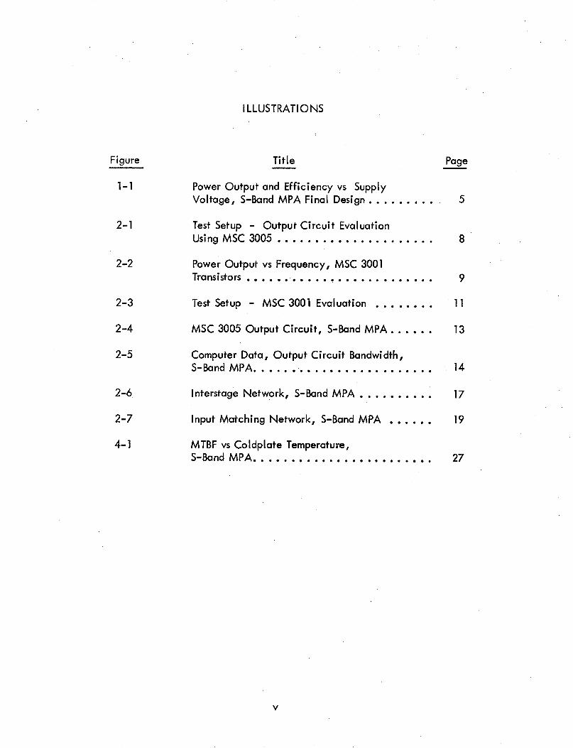
Figure Title Page
1-1 Power Output and Efficiency vs SupplyVoltage, S-Band MPA Final Design.......... 5
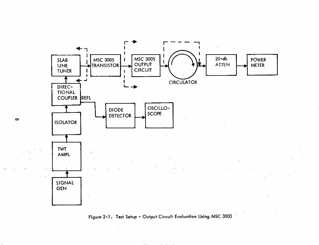
2-1 Test Setup - Output Circuit EvaluationUsing MSC 3005 .... ............. . 8
2-2 Power Output vs Frequency, MSC 3001Transistors ......................... 9
2-3 Test Setup - MSC 3001 Evaluation ........ 11
2-4 MSC 3005 Output Circuit, S-Band MPA ...... 13
2-5 Computer Data, Output Circuit Bandwidth,S-Band MPA . ............... 14
2-6 Interstage Network, S-Band MPA .......... 17
2-7 Input Matching Network, S-Band MPA ...... 19
4-1 MTBF vs Coldplate Temperature,S-Band MPA. . . . . . . . . . . . . . .... 27
v
TABLES
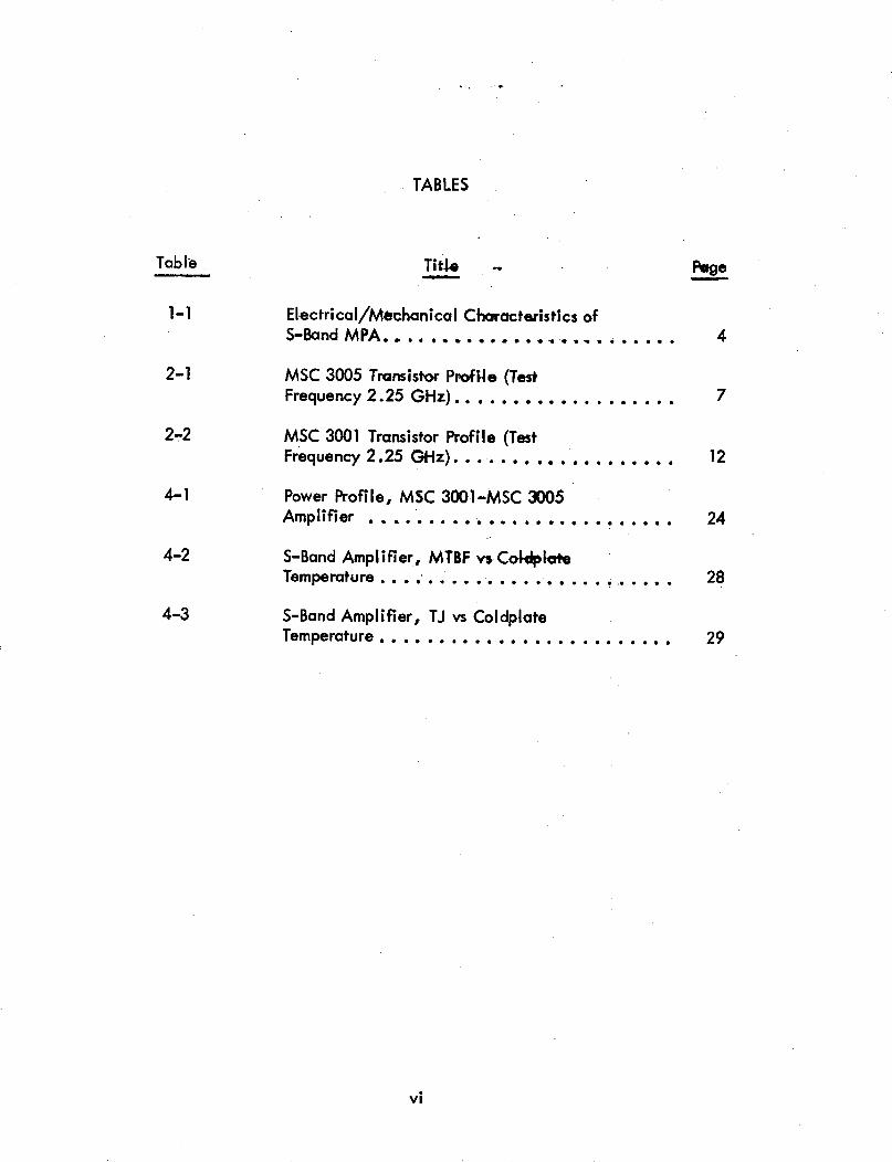
Table Title .a, Pege
1-1 Electrical/Mechanical Characteristics ofS-Band MPA. ........ . . . . 4
2-1 MSC 3005 Transistor Profile (TestFrequency 2.25 GHz).. 7
2-2 MSC 3001 Transistor Profile (TestFrequency 2.25 GHz) ........... ...... . 12
4-1 Power Profile, MSC 3001-MSC 3005Amplifier ..... ...... 24
4-2 S-Band Amplifier, MTBF vsCokidplteTemperature .. 28
4-3 S-Band Amplifier, TJ vs ColdplateTemperature ..................... ... 29
vi

2
1.0 DEVELOPMENT
The development effort associated with the S-Band Microcircuit
Power Amplifier took place over a period of approximately 12 months, com-
mencing in November 1970. A considerable portion of this effort, in its
initial stages, was expended in collecting information on available devices
which could be utilized in S-Band poweramplifier design. The criteria
used in this survey of the state of the art were power efficiency and gain
margins.
Following receipt of appropriate vendor information, a number
of circuit configurations were constructed and tested. However, because
of inadequate device characterizations, the results of these experiments did
not come up to expectations in spite of the fact. that test jigs had been
constructed to permit definitive tests and measurements of all pertinent
S-Band parameters.
Among the parameters checked, and which formed design criteria,
was transistor parameter spread, especially as it affected the amount of
available tuning adjustment. Among other considerations were mech-
anical packaging and thermal characteristics of the devices under test.
Various mechanical layouts were studied during the development
stages of the S-Band Microcircuit Amplifier, with emphasis primarily on three
styles of construction. The differences among the three revolved around the
number of circuit substrates to be used, the mounting of the device to its heat
sink, and the mounting of an output isolator.
The extensive te-t and selection program resulted in choice of the
MSC 3001 device for the input stage of the amplifier and the MSC 3005 for the
output stage.
1
Following preliminary development of the amplifier using the
MSC 3001 and MSC 3005, a Preliminary Design Review wasiheld (16 April
1971). In this review, all aspects of the proposed design were investigated
and suggestions were made for improvements in size and performance.
For the purpose of selecting the desired MSC 3005 devices, a
trip was made to the vendor (Microwave Semiconductor Corporation). The
criteria used in selection of the MSC 30 0 5 's were power output, efficiency,
and gain at 2.3 gigahertz. Thirty devices meeting these critieria were
selected. Ao -
The electrical design effort concentrated on the design of the /
output circuit to optimize power output from the MSC 3005 trn-iiisifter. With
this data available, the input and interstage circuits were then developed.
In-plant testing of the transistors showed a wider spread of
parameters than was anticipated, which caused some difficulty in deriving a
suitable circuit. The final design configuration proved to be very satis-
factory, however, since it included the ability to adjust circuit parameters
to compensate for variations in device parameters-..
Fabrication and testing of the prototype unit was completed and
the unit was subjected to the Qualification Acceptance Test as described in
the test procedure previously submitted to NASA/GSFC. The functional test
procedure was altered to allow computer analysis of the test measurements.
The test sequence and limits were not altered.
The prototype passed all qualification tests with only a minor
deviation, i.e., the input VSWR exceeded the limit of 1.4:1 by a small
amount, the amount depending upon temperature and drive conditions. The
efficiency degraded from a maximum of 40% (in the center of the band) to a
worst-case of 28% at maximum temperature (700 C), the degrading element
being the transistors.
2
An additional test was performed for information purposes only.
The unit was subjected to the same temperature extremes (-250 C to 70 C)
and a vacuum ranging from 1.5 X 10'3 Torr to 1 X 10-
7 Torr. This data showed
no corona problems over the pressure range.
The unit and Qualification Test Data were then forwarded
to NASA/GSFC.
The electrical and mechanical characteristics of the final design
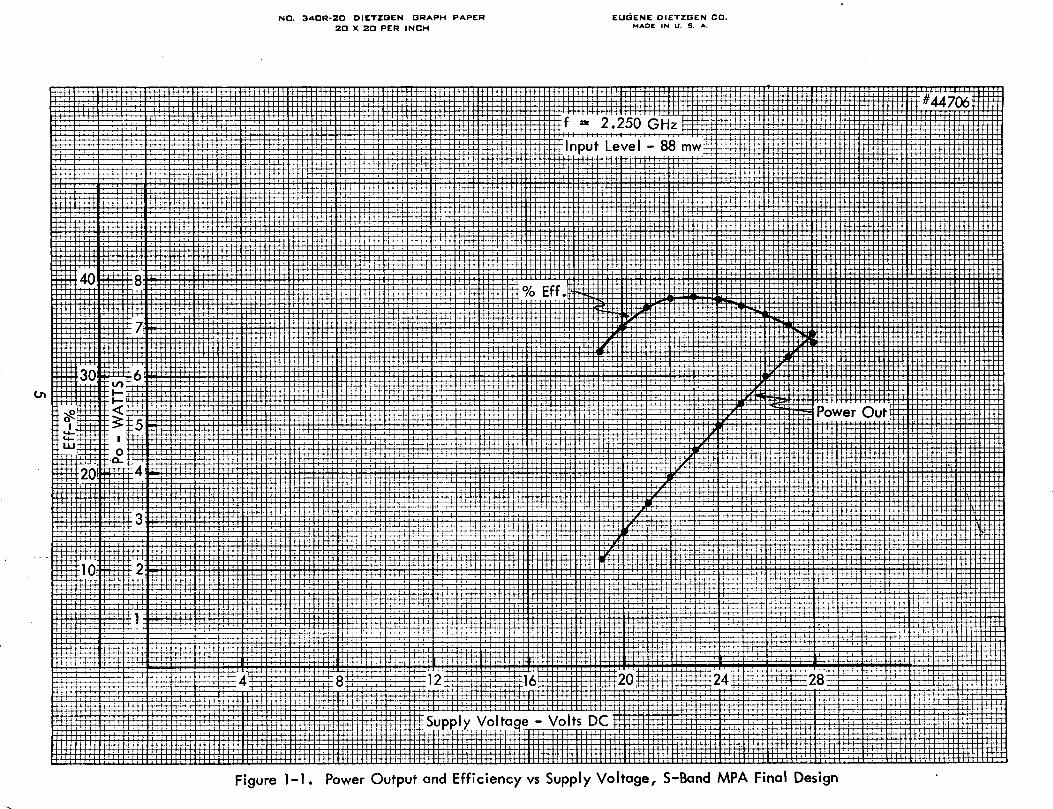
are presented in table 1-1. Performance is shown in figure 1-1.
3
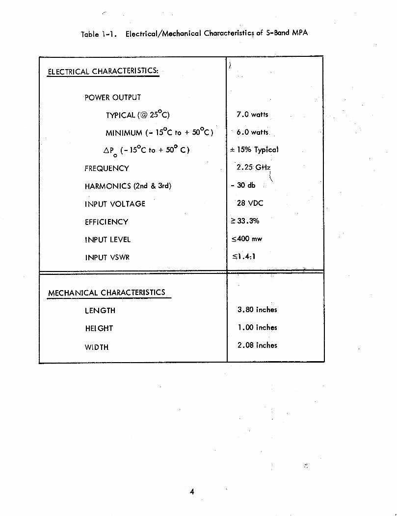
Table 1-1 . Electrical/Mechanical Characteristics of S-Band MPA
ELECTRICAL CHARACTERISTICS:
POWER OUTPUT
TYPICAL (@ 25°C)
MINIMUM (- 15°C to + 500 C)
AP (- 15C to + 500 C)0
FREQUENCY
HARMONICS (2nd & 3rd)
INPUT VOLTAGE
EFFICIENCY
INPUT LEVEL
INPUT VSWR
7.0 watts
6.0 watts
t 15% Typical
2.25:'GHz
- 30 db :
*28 VDC
> 33 .3%
_400 mw
-<1.4:1
MECHANICAL CHARACTERISTICS
LENGTH 3.80 inches
HEIGHT 1 .00 inches
WIDTH 2.08 inches
4
4l.
-0I 1ttt1t-tt
il I 1.11f2-0 -
1 - 1 1 . .
C li .I I II I IITTM
IIIII l 1 t IA
lIt:1 ft lt I Ht
i -i .' ,111:1 I'ttI
t.'
I ~ i +- t 4 H i U
l -h j lt H # 1
--t : f f 1 1 1 1 I f 1
Ifl+ L
-+HI-t -1-1H1 IH
I t
1-t-tTH
-H-H
t
t It t
I
ft tttf i: 4.
-41FFti t-:l
iti
IT-ill i i;i1
I H.
i: .11t-tt4- l B
lt l
I '1-4
FI
F
1 -F
I -F
--
14
RftH
4j-tMH
fff nufffilmThTh
l+
4 tl4i TR
h I
M4 M
It -Tttil-l 4flfl- ffIf iiii
4f-ji1f4=ff 1-14t1f4 jj 1ht>
Ml'U- N
O
-RI4lUH#S
I-in ~
tS -311M1t-1 -R
X at -4 11 :-:-
W
W~iftM-k0-0-tl-lDD-tti 7FIFT: l TFFT 9Fh4 r:-00T 4
:rr tt c l- t1 tt
cltF
: fe~
U
a- to
-- ~
~ ~
IIM
O
%- j ffiffi
1f -- ----
M~
i -:
..E
'-,StW-+ Mi __wtE
.X-k1X
11~ ~~
a
RM
!1-t 1 0 1
11
. U
Tlt~f flf if i 1
T
FF
tlir
5
FFlT4F
FTH-I-
20ttE
(N-- o
>
.0.6-.
II 0 4
.j
U-Co04-C"
O~faa
-DMMtMthS
1-t:
1LDO CI.
a,I0')L
L,
FM7
uP
rT7
7M
:=44
; rarP; I 1r-r1r
14,; .4 I itL
i ll I Il
..
-t ..1
1 _ ..la-lll
. W ~
-4 -t- --
tm-fill RUMT1I.. 1 11-11--11-m.''
''''' ' '{
~
' ''|~~' c'
| | .......4 +t .._.H
__.
P 4 I' 1 P ..
7 .
9 S
. L. ..:
'L'I'--i-'`--'---'``
'''-----'l-l'''ll n----'-
'li·--"'-----
_ ,,,,,
-,-i"l''l
..
..
.- ,,1
Ht
..7
11111
l 1 U +
..
J _I ..4
PW
T;4
.i
_ H I I I 4
H
I .;
_ .
i IT
illV
I !ll
I-t
W.-
.. .
I
':.
~i~iii~ilgim~w
i~~~M~
i~w~in~#tiitit,'i
W4
4.f 1.1W
ii~iii~ti~iiti~t I .. .g X g
~itff~··;i# ..
I
�4
.,
4lkI I "' I. .
, 1 tM
iT
3M-T T.-i
14i ' ]lt
ltlt ,_ :..t
i#XW+Ft~t
X~
iTW
i+t4
t-t'0e+3 FT'TSM
$'T O
t-tmX
Tlittti4O
it .
1t
1-!-11-tit~tt t 1 1:
1
1I
t~ttlt
.B
R.
' I I ti it
1ttl , I:t H
II
..
L .
..
I I I
I .
..
I I I
.i
.I I
..
..
I -I
--
-i
--
'U
I I-1 '
' I '
' I
'
R
-M
ll I 1 1- ~~~~~~~~~~~~~~~~ m I~~r1tit iiUt it~t~t:
'~- ~']~..].]] ~tit-[t ~~.:tL
I --I I
I EIf I
Hl+ H-H
--Ij 4 -. 1
-- 1t4ffitzt
-iF
Bi2
L
M1
-I--tiS
RI:t:fI
t iltltitttit-Hl:tlituil-
1 t
~ 1
4I 1
2.0 FINAL DESIGN
2.1 Device Characterization
The device parameters are of critical importance in the design
of the input, output, and interstage matching circuits for the MSC 3001 and
MSC 3005. The statistical spread of these parameters over a number of de-
vices required that each matching circuit be adjusted for the specific para-
meters involved. Device selection was used to minimize circuit adjustment
in the design of the S-Band Microcircuit Power Amplifier, but practical
considerations, such as device yield, limit the extent to which this method
can be employed to reduce the parameter spread. Therefore, it was necessary
to carefully characterize parameters of those devices which were used in the
prototype and flight units at the power level at which they operate. The
method of making these measurements was to mount the device on a test fixture,
optimize its performance with tuners on the input and output, and then look
into that part of the circuit of interest, using a Hewlett-Packard network
analyzer.
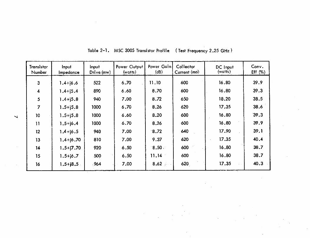
The MSC 3005 transistors were selected on the basis of their
output power, gain, and collector efficiency. For the vendor visit mentioned
in section 1.0, a test circuit was taken to Microwave Semiconductor Corpo-
ration in Somerset, N.J., and 30 devices were selected that would produce
a minimum of 6.5 watts with a maximum of 1 watt drive (matched with a
stub tuner) at a collector efficiency of greater than 35%. This eliminated
the need for adjustments on the output circuit, except for the tuning require-
ment. The devices were then further characterized in Radiation's laboratories
to determinine the spread of the input impedance. Typical results for 11 units
are given in table 2- 1, using the test setup shown in figure 2-1.
The characterization of the MSC 3001 transistors followed a
similar process. Since no selection was made on these devices, it was neces-
sary to first characterize their relative performance with respect to power
output and efficiency. An output test circuit was designed in which all
25 MSC transistors were operated with the input matched by means of a stub
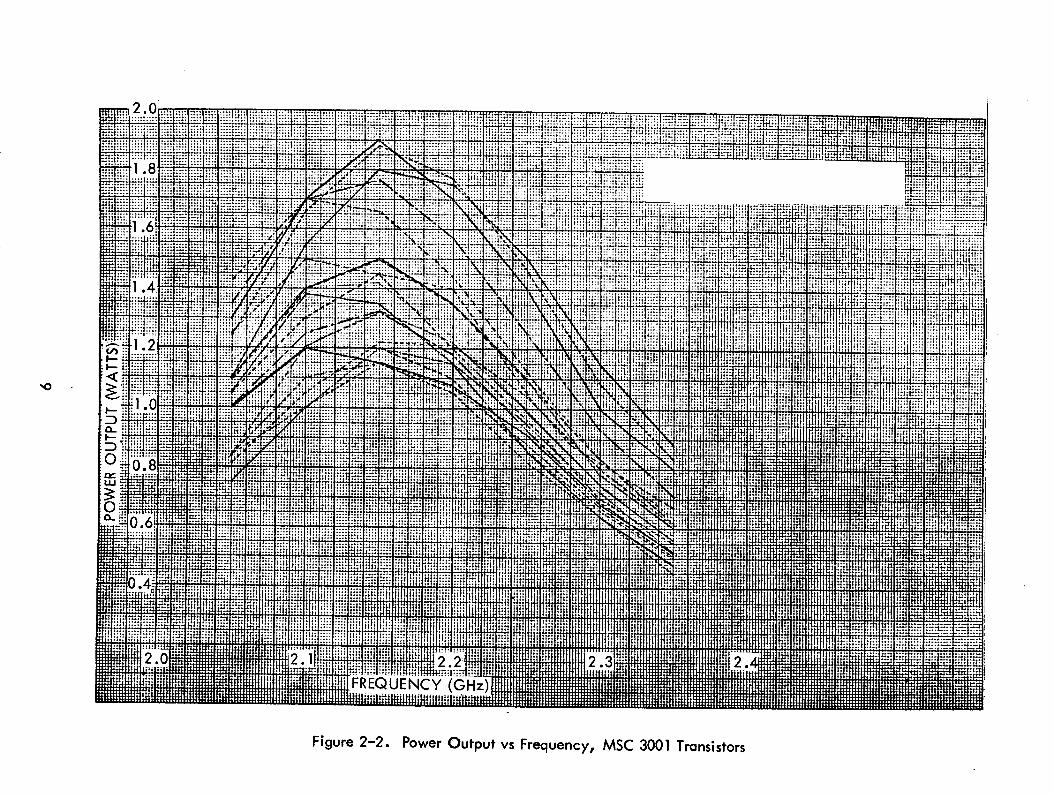
tuner. The resultant data, plotted in figure 2-2, shows the power output
capacity of the MSC 3001 devices, which permitted some matching of gain
6
U-
N
o',
0 0
It 0
0 I
o 0 0
C)
N
CQ
O
O
C
O
O
C
O
CO )
o 0
V
a L
oo vo
C
N
o vo
N
n Do
*o t
nC
4 0)
a U
U
4
C
.
._ C
>00
0 0
CO
N
0
3 C
4
0 O
O
O
O
%O O
CO
O
O
O
-C
O
C
'n
'0 '0
Q
o N .n
a
e E
@ )
>
)C
0%
0
oO
o o
%
CO
%
o
o
I-
* 00
o o a
CO CO
CN
N
N
I
I n
_ .)
.) .N
._
._
...._
._
2 _
_
7
r-,
ILI
L_=r-
0U
cL
1.000C
r,
U0) c0.0ILi
I-Ia-
0a-
InI-0)L
L
8
I
::: ?j: 'i
:i;:ii :
~"n~. :::*::-::: ::
:::: .*
:::~ ~ ~
~-] :'~
':: '~"' "'~
,: ,: :..... ; ,.I::::::: ,
.....
,.. ..
:I
!i !H!
(",
.,. ~
:::::1.
.......::::
MIt :
si i-
i::' .?
titm N
~~
~~
s! ;t'
: ^4= .t.o
j 1 -3 f i i3
m
w
i;, -
-W
i
i E
X
"'i :: E
. l
0 W
g
::~~
~~
~~
~~
~~
t
'.-.I~i~i! .... ... .... .o.
"'1 .. 1 t:_
,.,, .S,. ,., g . j.,-,g~g- i E W
IIW j: ji aH
JET
.1 ZG~lt
......... .T. T
=S-E,...
....~ .. , ..1 .... ......... ..iWW- «-
,,..}..ii..,i.,}f..,li.,,.j,.ixt. i''.n~ii~i it'..:.S
t W
%.Stii~f~ ~.s~iX.. .v ...
.. ,..
..}..
..
,...... t,
CV
): i -7
i i
.... ..-.. ... ... ... .... r
; ...*l ...? 1 --}-----N ff
CN
1:: :.:3,lX
_
: :: :4
*C t--j
,,, ., } C
X
t
C
i; F
;:': i j -le l r ;%itm
::L::::l::-~~~~r::: :::::::::
U~~C
iii ::,;::,::::.-:;:: :: ,Il~itiiiiiiiiiiliiiiii!~::iii ::
"C::::I::
;:tr::: ::1
~~
~~
~~
~~
~~
~~
~~
~~
~1
7::~::::L
;:::l::::t::::!::':1::::1::: ~i~fT.
1::::::1::::::: ::1:: .... ....
.. ... .I::r
·-·· ::r:::
4~~~~~~~~~~~~~~~~~~~~~~~~~~~~~~~~~L.... .....
..... ..
iIifi:: :;:,::::
:: i~~~~~~.fi ~ ~
:::::: O~~~
: ::I::.
C~~~~~~~~~~~~~~~~~~~~~4
fr:::r:: :
:~~~~~~~~~~~~~~ii II Q)~~~~~~0
"71 :: :.
.1.r. :: :l
::: L
L~~~~~~~~~~~~~~~~~~~~~~~~~~~~~~~~~~~~L
nt
I IT::;C:f-::n:
i .
.. ...
.. ..
.. .
.. ..
.7t:
:'. H
il
i: N::: ::t,.
... .. ......
::1::::1::::1::::1::::: :I:::~~~~~~iiifiiii~~ ~ ::::::
:::::::: ::::r.
... .... ..:::
~~
~~
~~
~~
~~
~~
~~
~~
~~
~~
~~
~~
~~
~~
~~
F:::::::I::::1::::
::: ::I: ::::·::: ::~ ~ ~ ~ ~ ~ ~
~~
~~
~~
~~
~~
...... ...... :::::::]::
::::: ::::I:;;:·.:
:::::I:; :
N:::
:: ::::::: :~ji~i
.. .... .... .. ...... ... I '::: -
-ii W
13111 :::
:::I::::if MC
Im MTONT::::::. ::il
IcC
: :: :I cb
N
04
I:
::· ::
: ...
_::::::: o
Ii ::::~
:: ::::
::::iiiC
,4; ~ ~
:::: 'ilii~
ifr~ii
.....
::::::::::i::~:::::::::.
1. :::,::: :: !i~tl
sivv/4
indin
o 4 3m
:::
9
characteristics between MSC 3005's and MSC 3001 's to achieve more uni-
form overall gain in the final two-stage amplifier. The curves shown in
figure 2-2 show that the devices peak out at about 2.15 GHz instead of at
band center. This was because the test circuit used was optimum at 100 MHz
below band center. However, this data correctly displays relative perfor-
mance of the devices.
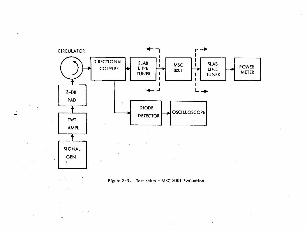
The next step was to perform complete characterization of the
MSC 3001 devices. The test setup for this series of tests in shown in figure 2-3.
A sample of three transistors was chosen from the spread in figure 2-2. These
transistors were then completely characterized for the parameters of interest.
This data is shown in table 2-2. The remaining 25 MSC 3001's were similarly
characterized at the same time.
2.2 Output Circuit
The finalized output circuit is shown in figure 2-4. This circuit
consists of a series of stepped transmission line sections on a 0.5 inch by 1.0
inch substrate, and is the circuit employed in collecting thedata shown in
table 2-1 using the test setup shown in figure 2-1 . The bandwidth of this circuit
was evaluated on the computer when driven from the MSC 3005 nominal out-
put impedance and loaded into 50 ohms. The results of this analysis, pre-
sented in figure 2-5, show the circuit to have an average 0.2-db bandwidth in
excess of 300 MHz. The computer data, as computed, is centered slightly
on the low side of band center, 2.25 MHz.
The final design configuration utilizes a variable at the inter-
face of the MSC 3005 collector circuit and the output substrate, in order to
accommodate the statistical distribution in the output impedance of the MSC
3005. It was determined that a single-element impedance inverter con-
structed in microstrip would allow the entire device spread to be matched.
The required variable is shown in figure 2-4 as element "A",
where 6.4 Q < Zo <15 Q and the available length from the edge of the
substrate to the edge of the case diameter is used as required. A fixed posi-
tion of the output device is used, which accommodates an input match more
easily and imposes no restriction on the output matching'circuit.
10
c0IM 0U.
u. U,nI-
C,
11
LI L
0 04
I)0
Xo
o E
U
at
.o
0 0 L
_
_
U~
C
3- u
II-O
>
0.A
.4-
-C
4
E 0
4) 4)
--
0 .
12
~. ~ 6.8 pfd Chip Cap0.10" Sq
.. .I
... _ .0 ..... !:ri A.
.050" Sq., ...... 0 /t---.o .
...~.~.j.................................
: --.'':.:.:.:.:.:. ',..:.~.i.~..:. :~.,.L.:,,:., ,.:.:.,.:.:.:.:.........
.0815 A
Figure 2-4. MSC 3005 Output Circuit, S-Band MPA13
)�· ··�·�·�·�·�·�·�·�·�·�· ·········-··I
: , : .......... .....
i
"""
50Q0
ENTER YJIN,'Y XX? ? . , *I'
PXIs: FROiM .
P .000
p 4,
P. 1 69
2 .2602.2R~
2@ 300P.322.3m0
COMP ND
1O 1 20 MAJOR INC = 0.20
I* ...... ,,. ......... *I ...**@*.I@O ...... ........ lOI S*@** .1....4
+4-
a
+.
+
+
4.
+
+
4.
OUTPUT NETWORK
3.5n 50n
* +
* +
* +
* +
* +
* +
* +
: +
.
Slop
FROGRPF' SlTOP PAl '
UNI I S
~0000 · 40 1CH
Figure 2-5. Computer Data, Output Circuit Bandwidth, S-Band MPA (Sheet 1 of 2)
14
0.3nh 0.3nh
4
4-
4
4-
00 IO .0A KC
li SED 1 '· -16F1'FP y 'F
(A ]7 7 rt R I -i1
::' JER ZG,/L,F1,FP2,NF?3.5, 502.Pe0,2.5,25
F c* i7.) i
2.0 602 .(?0
P.1 60? * 1 80
.2009 * ??02C>.2R
2 *-2"
? . .rn
¢. * '8
? * 50 0C. 5Li
(7OMiv~MND ?
VSWR '1L(.DB)1 .4z 67 0.15921- 397 V.121"1 .331 .$9?AzE-011 .271 .629/E-011 .17.`4263E-011 * 17 74-846E-011.1 45.2Q05/E-01I .39.1895E-011 .157.2373E-011 19-.349 E'01!1 .244.5244E-011.303.7631 I-011 .3671 .4371 512I .5911.6751.76A1 .8571 .g95,2.0562. 1 632.2 7 42 . 3909.5112 - 636
0. 10640.14260.* B490. 2 3290.28660 3k570. 4099(A. 1792
!. 55310.6314
. 1 39
0.89010 .9833
PhASE9 653
100.3
10632
110-.2112.2
1 16.2118. 1120.1
121.0125.9127-9129.8131.6133- 513 5 3137 *
1 38 * 9
I P4.1
I~.~·r
164.I
FR IN3.3223.2833.2Z63.2103.1 7 3.1403. 1073.0 75.3.0 453.0152.9862.9582.9302.9042.R792.8542. 8302 .8072 - 78 59.7642- 7432. 7232 70 32 68 52.667
649
X IN-1 -303-1 11 7
-0.9336-0 .751 3-0 . 570 4-0 * 3909-0.2128
3606E-0 I10.139/40.31 360.48650 65820.82870.9981
1 *1661 .333I .4991.6641 .8281 9912. 1 532.3142 ·-4742.6332.7912.948
R UT X OUl51 78 19.5*51 72. 16.9951 33 14.4850.6/ 12.0849.67 9-81 5A8 .46 7. 73647.05 5.86745. 47 4.22643.78 2.82242.02 1 · 65240.21 0 .71 1I 38 39 129 7E-O 136. 58 -0 . 537z3 -8 1 -0 8 79 433- 10 -1-05831.1 45 -!. 09129.86 -0.997728 .36 -!0 794126.93 -0 · ̀49 6025-59 -0 11722 . 32 0.329723i13 e*833922.01 1 38620.96 1 .97719.98 2.60119.06 3-251
Figure 2-5. Computer Data, Output Circuit Bandwidth, S-Band MPA (Sheet 2 of 2)
15
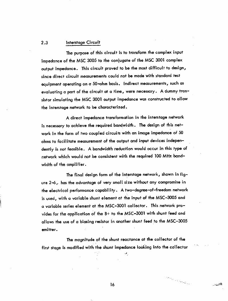
2.3 Interstage Circuit
The purpose of this circuit is to transform the complex input
impedance of the MSC 3005 to the conjugate of the MSC 3001 complex
output impedance. This circuit proved to be the most difficult to design,
since direct circuit measurements could not be made with standard test
equipment operating on a 50-ohm basis. Indirect measurements, such as
evaluating a part of the circuit at a time, were necessary. A dummy tran-
sistor simulating the MSC 3001 output impedance was constructed to allow
the interstage network to be characterized.
A direct impedance transformation in the interstage network
is necessary to achieve the required bandwidth. The design of this net-
work in the form of two coupled circuits with an image impedance of 50
ohms to facilitate measurement of the output and input devices indepen-
dently is not feasible. A bandwidth reduction would occur in this type of
network which would not be consistent with the required 100 MHz band-
width of the amplifier.
The final design form of the interstage network, shown in fig-
ure 2-6,. has the advantage of very small size without any compromise in
the electrical performance capability. A two-degree-of-freedom network
is used, with a variable shunt element at the input of the MSC-3005 and
a variable series element at the MSC-3001 collector. This network pro-
vides for the application of the B+ to the MSC-3001 with shunt feed and
allows the use of a biasing resistor in another shunt feed to the MSC-3005
emitter.
The magnitude of the shunt reactance at the collector of the
first stage is modified with the shunt impedance looking into the collector
16
6.8 pfd Chip Cap
6.8 pfd Chip Cap
Shunt Feed B+Bias Provision
ADJUSTABLE SERIESELEMENT
MSC 3001 Collector
ADJUSTABLE SHUNT ELEMENT
MSC 3005
EMITTER
Figure 2-6. Interstage Network, S-Band MPA
17
feed circuit, and thereby establishes the unique driving point impedance
locus desired as an input to the interstage matching network.
2.4 Input Circuit
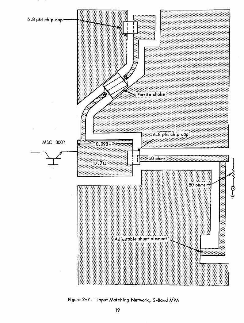
The purpose of this circuit is to match the MSC 3001 input
impedance to 50 ohms. Since the magnitudes of the impedances involved
are only slightly greater than 2 to 1, adequate bandwidth can be achieved
with a relatively simple network. However, the circuit must be capable
of adjustment, since the input VSWR must be held to a value of 1.4 to 1 or
less across the band of 2.2 to 2.3 GHz.
The final circuit configuration of the input matching network
for the amplifier is shown in figure 2-7.
A three-element network is used to attain the required matching.
A two-step inverter is placed in series with the MSC-3001 emitter, followed
with a variable element shunt transmission line. The shunt line length is
adjusted to obtain the desired value of the reflection coefficient at the in-
put port to the amplifier.
The desired operating point in the circuit is obtained with a
shunt feed to the emitter on the substrate. A ferrite type of choke is used
in the feed to control the Rp placed in the emitter at the out-of-band fre-
quencies.
Until the MSC 3001 or MSC 3005 is driven to the point where
no further power output is obtained with increased drive, the input imped-
ance varies widely with increasing drive (with its accompanying increase in
collector current). Increasing the drive beyone this point of power output
saturation drives the DC current up and increases the power the device must
dissipate. Ideally, therefore, it is desirable to operate both the MSC 3005
18
6.8 pfd chip cap-
MSC 3001
I
...... .,...................................................... ..................................: :~~~~~~~~~~~~~~.:.:.:.:..... .:.:...s. ........... .,.,.:..:.:::::.:.:
:::::::, ~~~~~~~~~~. ,............... ,Zo. ............ . . . . . . . . . . . . . . . . . . . . ... :...::..::::......::
:::::::: :.::: :::::X~~~~~~~~x a. ... .... :--. ::... ....... : .. . . .::::::::::::::::::::::~~~~~~~~~~~~~~~~~~~~.. .X . .. . . ., . -.: . .....--.-. :-.::.......
::::::::::: :XS 5 ~~~~~~~~... ............................-. ::-:.:.-.-.-.-.-..-. -:.-
::: :':·:I::::::: :::: ::: -:-:-:.................:.:..:.:.:.:.:. .:..:.:.
:-::::::::~~~~~~~~~~~~~~~~~~~~~~~~~~~~~~~~ . . . . . . . :.: . .. :: .::::::::::::: :y , / , o ~~~~~~~~........ ....................... :.: :.:.::.-.
:::::: :s / - ~~~~~~~~~~. ............................ .-: ... ---.
:::: / w ~~~~~~~~~~~~~~.......... sy-.........,,-.- .. ::.-.-.-.-.-.-.-........ ....... :..::/ s- Z A ~~~~~~~~~~~~~~~~~~~~..................... %........... ....... ,- .. :.:.-.:.-.--.......
r /s /-~~~~~~~~~~~~~~~~~~~~~~~~........ ...........~~~~~~~~~~. .. . .......................... .:.. :.... . .. . ...
iii . . .. . . ....
I ' .. ·. ·.' "'''''''':"-....... . .................
~~~~~~~~~~~~~.............. ....... *****...-.-.-.-*.......... ... ----*****... ..~~~~~~~~~~~~~~~~.-..... ..----------...-............. ,......... .......-.-.-.-.-.-.-.-.-.-........... -: [::: . .:.6. ..pfd.........:..:::.::...:.:.::::::::::. ............. .............C::::i Ferrite choke ........................
...............::.~................... .... ......... ..""" "" "............................ . .....' ,'.. -........ . ......
'.''' ··········.... ,. ..... ..... .............. ......... ........ ......... ......... .................................... % ............. ................................ ...............................................
................ ···''''i··· ''''··· ''''····'·' ··· ·· · · ·· · · ·· . .. . .
·'·'·'·'·'·'·'·'·'·'.'.:........ :Ole ................ .... .................................... ·...... ... . .. . ..... ......... ... . ..... ..... .....'·'·'·'·'·'·'·'·'·'·'·' ··'·'·'·'·'·'·'· ''.............................................. ...'.
~~0 .0 9 8 X ........... ....''·'' ··:::: ::·:. ................ . ....... ...:'·'·........... .''.'.'..`.`.- .a .........................·.·.
-1
............ ... . ............ ...........50 ohms :: :-: ·::.:::::.:1.7Q : :: ......... : @; ............................... .. ................. wi ::::::::.::.:.:.::::::::::::::::::::::::::::::::::::: ..."::. o . .......... :.. .. I.
............. :... .. '''.''::. : .. . . ................ohms. .... ... ......~~~~.. .. ...... .. ... .,,.. '^
....v. .................................::::: ... v...
·~j~iiiiii~iiiiiiii~iriiii oohms iiiiiiitiijiiiiiiiiiiiiiiijiiii..........
'jjjj jiiiiiiiiiiiiiiiiiiiii iiiii'iiii irijijiiiii
.......... iiiiiiiijiii~ii-,-.'.:-.'-.--.jidjustab~e shunt element.
~ii j~~~iii~~~iiii~~iiii~i .iiiii iiiriiiiiiiiii.. .iiiiiiii............. ................jiiij
i~iiiiliiiiiiliiiriii. . .................ji~i~ii~i~ii~i~jj~i~~i ... ......ii
Figure 2-7. Input Matching Network, S-Band MPA
19
........................................ v.v.v.v.v.v.v.v.v.-.:.... : .:.;?................................ v... ::::::: ···.· :.:.:.:.:.:.:. :~: ::::::::::: : .

and the MSC 3001 at the drive level at which both are just into saturation.
This assures maximum collector efficiency in the MSC 3005 stage and mini-
mizes the input VSWR to the MSC 3001 stage. In order to accomplish this,
the devices were selected on a basis of device saturated gain. If the spread
of transistor gain was too great to allow both transistors to be operated op-
timally in saturation, the MSC 3001 was operated at a drive level just suf-
ficient to drive the MSC 3005 into saturation and the resulting MSC 3001
input mismatch was corrected.
20
ASSEMBLY AND ALIGNMENT
Reference to the assembly drawing (RAD 417775G-2) will disclose
that the chassis assembly is completed with the input, interstage, and output
substrates soldered directly onto the chassis. This is the final step in the
integrated procedure of assembly and alignment. All connections are made
except those to the transistors.
The transistors are then bolted into position with the MSC 3001
device physically located as near to the input substrate as possible, for mini-
mum emitter lead length. The MSC 3005 device is located as near to the
output substrate as possible, for minimum collector lead length. All connec-
tions are then made to the device collector and emitter leads'uti-lizing a silver
base epoxy without hardener.
A general measure of performance is obtained with this test
configuration as follows:
a) The output tuning is achieved by adjusting the collector
lead inductance. This is done utilizing a narrow piece
of copper foil overlaying the collector lead. If the out-
put circuit tunes high, the MSC 3005 device is moved
away from the output substrate, and the test 'is-repeated.
b) Interstage tuning is achieved by adjusting the stub length
at the MSC 3005 input. The stub length is varied by
pressing a shorting bar of copper foi l across the stub at
the desired location. At this point no tuning is required
at the input of the MSC 3001 device.
In general, power output increases about 20% to 30% when
final solder connections are made. Most critical of these is the soldering of
the transistor base to the chassis.
21
3.0
If the results of this preliminary test are favorable (i.e., both
the interstage and output stages can be tuned), the device is then soldered
into position utilizing reflow solder techniques.
Once the devices are properly soldered into position, the output
and interstage tuning is adjusted with copper foil, as previously described.
When optimum tuning is established, the foil is permanently soldered into
position. Final adjustments are made by cutting away small increments of
the foil after it is soldered into position.
The following considerations apply throughout the assembly
and alignment:
a) A noncorrosive, nonactivated flux is utilized when
making solder connections, especially those which
will react with the chassis material (in this case,
aluminum).
b) All surfaces are kept clean during the preliminary
testing, when there are no solder connections to the
devices. (Fingerprints and other foreign material
between the base of the device and the chassis will
drastically reduce power output).
c) When the MSC 3005 device is located away from the
output substrate for purposes of tuning, power output
is lowered considerably. If at all possible, the output
is tuned with the MSC 3005 contacting the chassis at
the output substrate.
d) The current drain of each stage is monitored separately
to avoid exceeding the power rating of the devices.
22
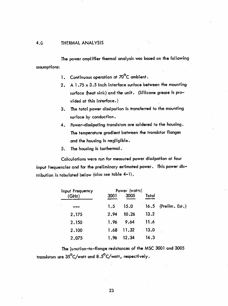
THERMAL ANALYSIS
The power amplifier thermal analysis was based on the following
assumptions:
1. Continuous operation at 70°C ambient.
2. A 1.75 x 3.5 inch interface surface between the mounting
surface (heat sink) and the unit. (Silicone grease is pro-
vided at this interface.)
3. The total power dissipation is transferred to the mounting
surface by conduction.
4. Power-dissipating transistors are soldered to the housing.
The temperature gradient between the transistor flanges
and the housing is negligible.
5. The housing is isothermal.
Calculations were run for measured power dissipation at four
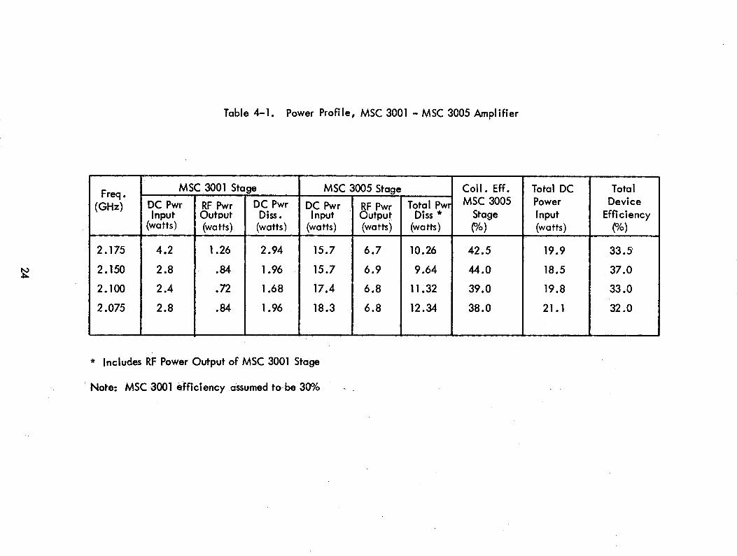
input frequencies and for the preliminary estimated power. This power dis-
tribution is tabulated below (also see table 4-1).
Input Frequency Power (watts)(GHz) 3001 3005 Total
1.5 15.0 16.5 (Prelim. Est.)
2.175 2.94 10.26 13.2
2.150 1.96 9.64 11.6
2.100 1.68 11.32 13.0
2.075 1.96 12.34 14.3
The junction-to-flange resistances of the MSC 3001 and 3005
transistors are 350C/watt and 8.50 C/watt, respectively.
23
4.0
.'o
o o
oo
2
.O
.a
a
UJ.
in U
O
O
O
/~
,.,_
O
C)
=N
.U
)c&) O
C
) 0 0
02U
. .
_.
, ao
8o-C
S
C0i CVZ
10 C
C·I ~
~ ~
~/r)
yo ~
-'
C
, n
'.. co
o 00
0~pe
O1
00
ao
0)
"oL *
* .
-. '-
ji~~~~~~~~~~~~ u
Z
24
L-
0ItUr, 0O0 ULnI
0 0U:2oIV0,0I0 I- 0)0-
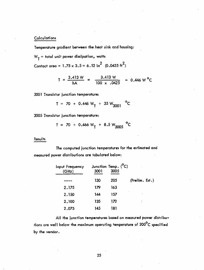
Calculations
Temperature gradient between the heat sink and housing:
WT = total unit power dissipation, watts
Contact area = 1.75 x 3.5 = 6.12 in2 (0.0425 ft2)
3.413 WT =-=hA
hA3.413 W
100 x .0425 0.446WC
3001 Transistor junction temperature:
T = 70 + 0.446 WT + 35W3 0 1WC
3005 Transistor junction temperature:
T = 70 + 0.466 WT + 8.5 W3 0 0 5 C
Results
The computed junction temperatures for the estimated and
measured power distributions are tabulated below:
Input Frequency(GHz)
2.175
2.150
2.100
2.075
Junction3001
130
179
144
135
145
Temp. (C)3005
205
163
157
172
181
(Prelim'. Est.)
All the junction temperatures based on measured power distribu-
tions are well below the maximum operating temperature of 2000 C specified
by the vendor.
25

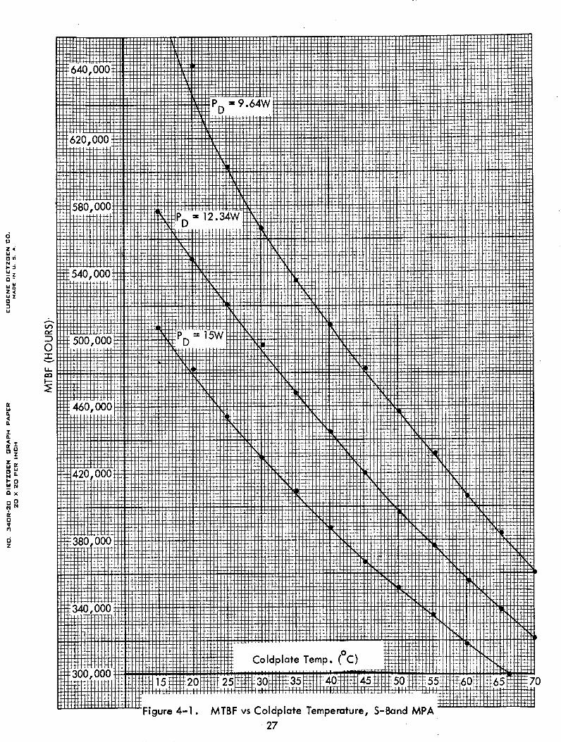
Figure 4-1 and table 4-2 depict MTBF vs coldplate tempera-
ture for three different power distributions, while TJ vs coldplate tempera-
ture will be found in table 4-3.
26
640,0
PD 9
620,
Fl4 H t--- H- - + t t -HL4-444444 44
.... G ...... 1 W4-4
580, 0004fl t P .12.34WD
III4-f
Wtit 0t~t~t~ 4flfttf4t~0 t4t~f Ht- iI-it f lfi:4 f ttt I M 1 l l -tl
· 'f ' ' E ' T ] ' . 'I2 . . . . . . . . . . . . ..
= 15W
W~~~~~ It I- -T r:ltI 7I ~ ~ T1-
f l t! i ft-bWI444 -4-1H { iF 1-W 1-F- -1 I i-i T 14 T-i-.- 4-4- .4-44T-14:1: I:TI Itfftf4114fifti fttt-I t I t Ii L ++ ttN+ It-t t It 1-I ititf+t t~ft 'TTI 14 -tFIttI ti -th-tPII UIE.Itt.t -tqt 4l'I t 1-i 4't4- ? J-]-
PltI I IfP-Htitfttflfit
f MtItIt _.:H tTtt-ti i ttlt4
t t TT #fff-bht * - tI Itt ' i-4'Tt t .
t1lt:i
44 f-4
F 4T Ii0
tH-4t-1--
RWtR4R
0l--Otf'H - IThiLliif I
K I-1Wtf- fTT1tUTmfi444-1WI0
:ttt- l Ptn n. # 4K 300,000Coldplate Temp. (0C) it'Htfitit4$-lltH X
15 20~. 25 _: 30i:k5 !40,-1145A :~. 5 I5~~t0t[: 't1111111 1111 1 .11 1111H111111;:1,11,*.T1T1111Z1 .ZTT11111111IIIIIII ll.II 1,1111.1111..111.1.,11' lLItIJ:, l I..I..L 4
[Hth-I4':Figure 4-1. MTBF vs Coldplate Temperature, S-Band MPA
27
i-flfi,_ 4-.- 44-,L
d024LiOwN
r zz r-
w '
'I
w:tLi
:H-H
,40,000 .:tm-:H:H.i
O C0ILL
' 460, 000)Wn.
4.
I0.<
z
I-0,a
ox
0
¢1
d
0ItM
z C38000
340 01
7
_- .M- JXlIMt0f,
Hii ttf-f Rff
1-1-v j.1 ................ . I ~t!t 101 . .
t'l 1 1tj t-tl t III M It[TTXTT-rl IITTI T-FTT T-T-I III III II Ft I - i 44-44-4444-444 1 1 1 1 1 1 i i i 1 i 1 i 1 1 1 1 1 1 1 1 1 1 1 1 =T I Tttt- f rr rIII
..W . . Wm1. +t#+44} I 11 I IH++ttHH+ Hifi ftf-tt-tf+
tll lill r tflxtrrtlll
1rt I 1 14 1 11+N 1- Ftfi
... 1 i. i L a i ..I i I I I .. . .. . ......., ,_-_.- L~ . P1-f'1tt1 I tt t t lt tt'tt TLL tI4
-RME.7
U.
-
R
i II -I -I
H-t+
4-1-4tI
4
i
tt-mltl
WA-tl~~~~~~~~~~~~~~~~~~~~~~~l~~: I X Xj4
H H4l: t'tH' f i-;
io
.l--Pt-tf�tff-Kttt:M-tttf I
1t~~i~ MNM-9tt-]t
,,
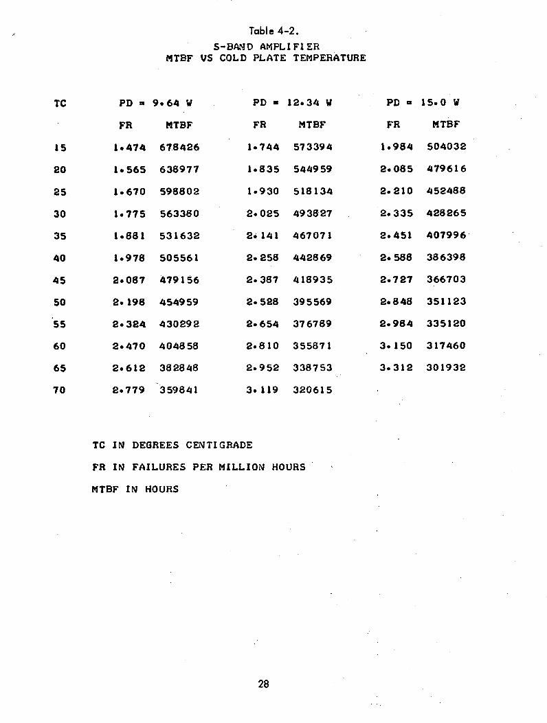
Table 4-2.S-BAND AMPLIFIER
MTBF VS COLD PLATE TEMPERATURE
PD =
FR
1.474
1.565
1.670
1.775
1.881
1.978
2.087
2. 198
2.324
2.470
2.612
2.779
9.64 W
MTBF
678426
638977
598802
563380
531632
505561
479156
454959
430292
404858
382848
359841
PD -
FR
1.744
1.835
1.930
2.025
2. 141
2. 258
2. 387
2. 528
2.654
2.810
2.952
3. 119
12.34 W
MTBF
573394
544959
518134
493827
467071
442869
418935
395569
376789
355871
338753
320615
TC IN DEGREES CENTIGRADE
FR IN FAILURES PER MILLION HOURS
MTBF IN HOURS
28
TC
15
20
25
30
35
40
45
50
55
60
65
70
PD a
FR
1*984
2.085
2.210
2.335
2.451
2. 588
2.727
2. 848
2.984
3.150
3.312
15.0 W
MTBF
504032
479616
452488
428265
407996
386398
366703
351123
335120
317460
301932
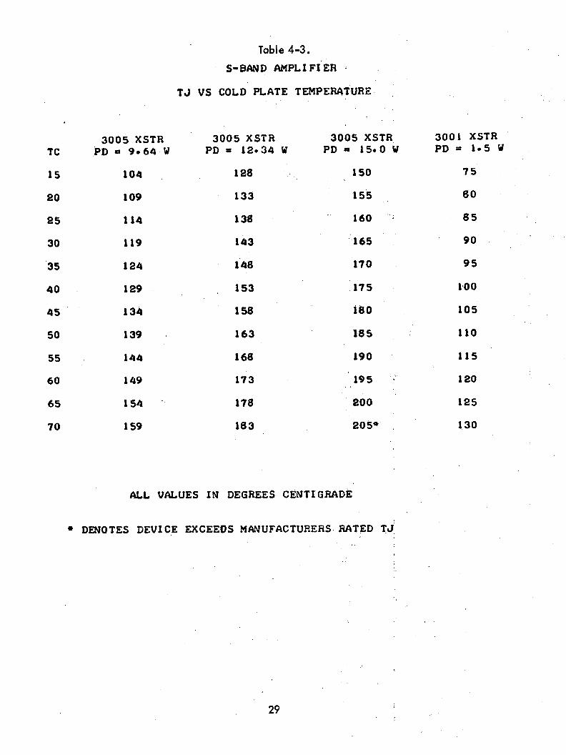
Table 4-3.
S-BAND AMPLIFI'ER
TJ VS COLD PLATE TEMPERATURE
3005 XSTRPD = 9.64 W
104
109
114
119
124
129
134
139
144
149
154
159
3005 XSTRPD = 12.34
128
133
138
143
148
153
158
163
168
173
178
183
3005 XSTRw PD - 15.0 W
150
155
160
165
170
175
180
185
190
195
200
205*
3001 XSTRPD = 1.5 W
75
80
85
90
95
1'00
105
110
115
120
125
130
ALL VALUES IN DEGREES CENTIGRADE
e DENOTES DEVICE EXCEEDS MANUFACTURERS RATED TJ
.I
29
TC
15
20
25
30
35
40
45
50
55
60
65
70