Embed Size (px)
Citation preview
Applied Materials Confidential| External Use
R2R Vacuum Tool Architecture
and Processes for Next
Generation Display Devices
Dr. Fabio Pieralisi
Applied Materials WEB Coating GmbH
2016FLEX Europe, Grenoble, France
26th October, 2016
| External Use
Safe Harbor Statement
This presentation may contain forward-looking statements, including those regarding Applied's products, industry
outlooks, strategies, opportunities, and opportunities. These statements are subject to known and unknown risks and
uncertainties that could cause actual results to differ materially from those expressed or implied by such statements,
including the level of demand for Applied's products, which is subject to many factors, including uncertain global
economic and industry conditions, demand for electronic products and semiconductors, government renewable
energy policies and incentives, and customers’ utilization rates and new technology and capacity requirements; the
concentrated nature of Applied’s customer base; Applied's ability to (i) develop, deliver and support a broad range of
products and expand its markets, (ii) execute its acquisition strategy and realize expected synergies, and (iii) attract,
motivate and retain key employees; and other risks described in Applied Materials’ SEC filings. All forward-looking
statements are based on management’s estimates, projections and assumptions as of February 16, 2012 and Applied
undertakes no obligation to update any forward-looking statements.
This presentation also contains non-GAAP financial measures, along with reconciliations to GAAP.
| External Use3
Outline
Short introduction to Applied Materials
► Enabling & accelerating innovation
► R2R business unit
Applications & megatrends
► Internet of things
► Wearable devices
► Wide Colour Gamut Displays
Key R2R processing technologies
► R2R CVD, PVD & etch
► Patterning technologies
R2R barrier & thin film transistor processing
► Barrier layers & stacks for integration in mobile, wearable and large-area displays
► Flexible TFT backplanes processing for sensors & low pixel density reflective displays
Hybrid approaches to IoT & wearable device manufacturing
Summary
| External Use
Introduction to Applied Materials
| External Use
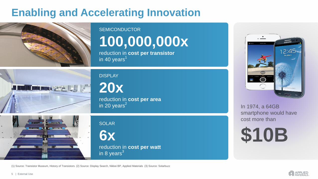
Enabling and Accelerating Innovation
In 1974, a 64GB
smartphone would have
cost more than
$10B
SEMICONDUCTOR
100,000,000xreduction in cost per transistor
in 40 years1
DISPLAY
20xreduction in cost per area
in 20 years2
SOLAR
6xreduction in cost per watt
in 8 years3
(1) Source: Transistor Museum, History of Transistors (2) Source: Display Search, Nikkei BP, Applied Materials (3) Source: Solarbuzz
5
| External Use
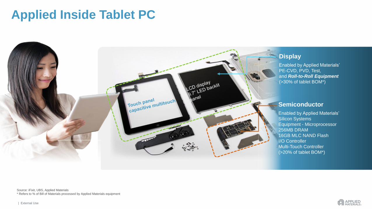
Applied Inside Tablet PC
Display
Enabled by Applied Materials’
PE-CVD, PVD, Test,
and Roll-to-Roll Equipment
(>30% of tablet BOM*)
Semiconductor
Enabled by Applied Materials’
Silicon Systems
Equipment - Microprocessor
256MB DRAM
16GB MLC NAND Flash
I/O Controller
Multi-Touch Controller
(>20% of tablet BOM*)
Source: iFixit, UBS, Applied Materials
* Refers to % of Bill of Materials processed by Applied Materials equipment
| External Use
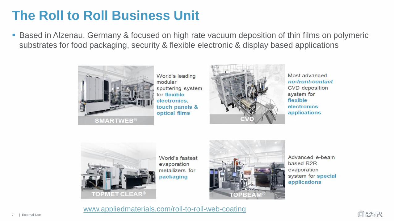
The Roll to Roll Business Unit
Based in Alzenau, Germany & focused on high rate vacuum deposition of thin films on polymeric
substrates for food packaging, security & flexible electronic & display based applications
7
www.appliedmaterials.com/roll-to-roll-web-coating
| External Use
Applications & Megatrends
| External Use
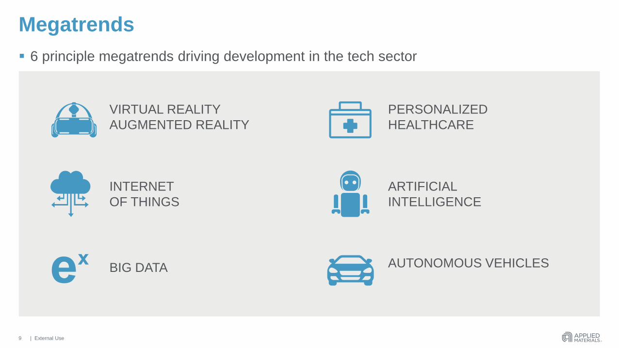
Megatrends
6 principle megatrends driving development in the tech sector
9
VIRTUAL REALITY
AUGMENTED REALITY
INTERNET
OF THINGS
BIG DATA
PERSONALIZED
HEALTHCARE
ARTIFICIAL
INTELLIGENCE
AUTONOMOUS VEHICLES
| External Use
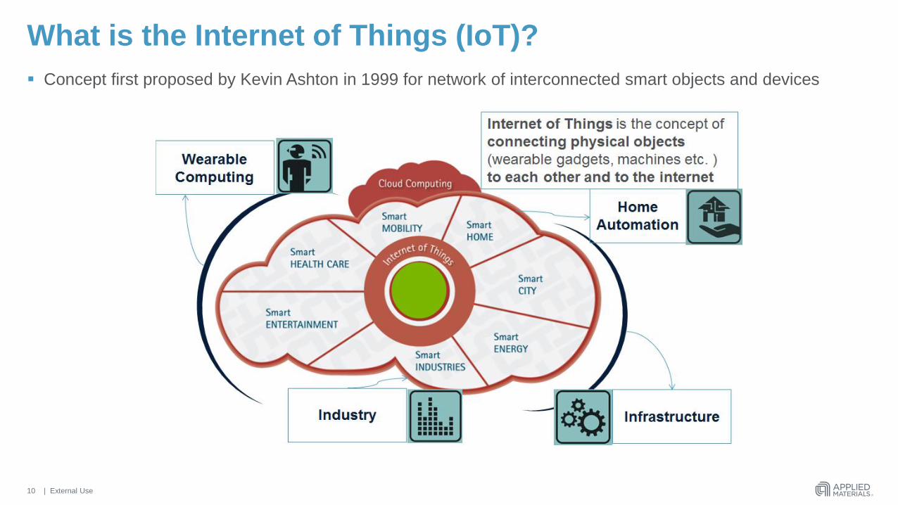
What is the Internet of Things (IoT)?
Concept first proposed by Kevin Ashton in 1999 for network of interconnected smart objects and devices
10
| External Use
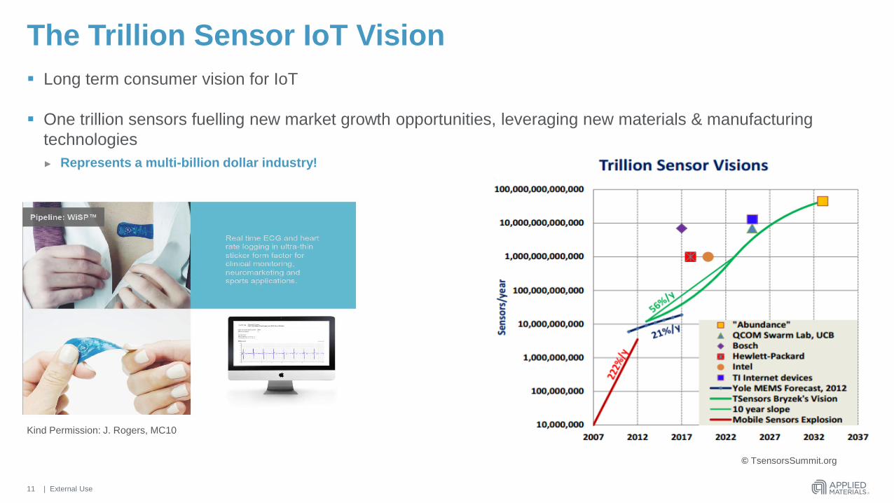
The Trillion Sensor IoT Vision
Long term consumer vision for IoT
One trillion sensors fuelling new market growth opportunities, leveraging new materials & manufacturing
technologies
► Represents a multi-billion dollar industry!
11
© TsensorsSummit.org
Kind Permission: J. Rogers, MC10
| External Use
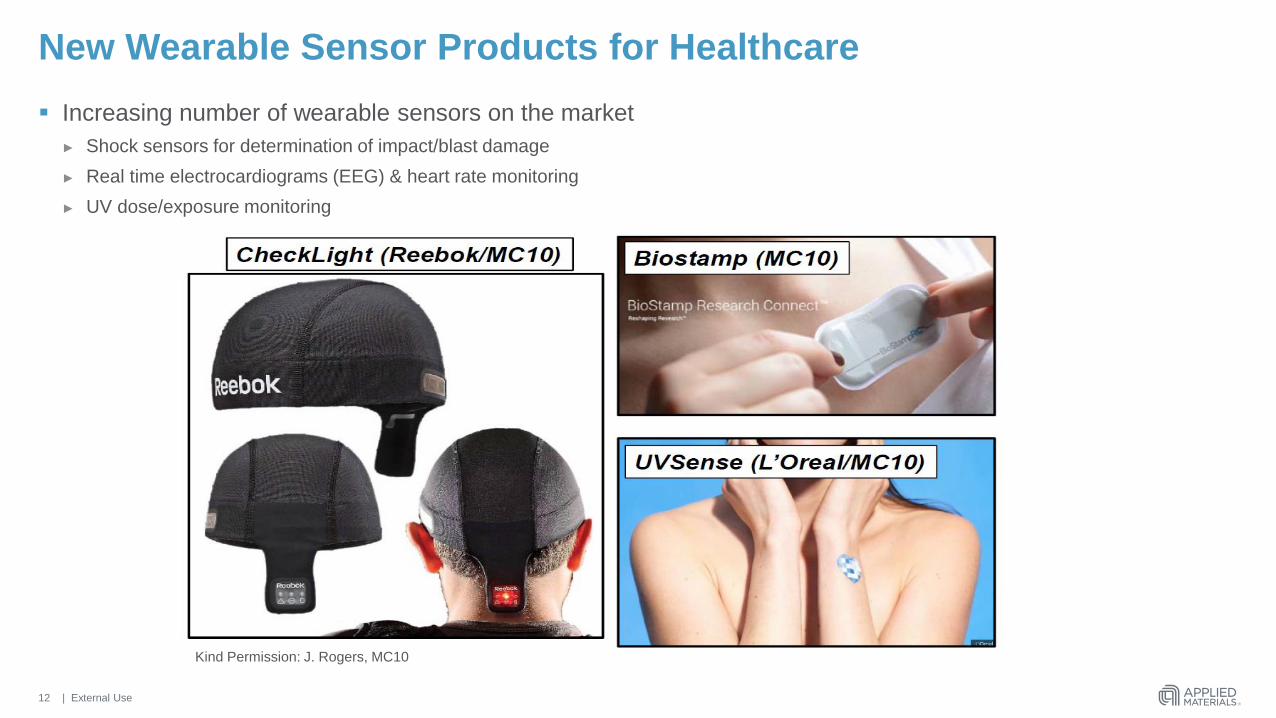
New Wearable Sensor Products for Healthcare
Increasing number of wearable sensors on the market
► Shock sensors for determination of impact/blast damage
► Real time electrocardiograms (EEG) & heart rate monitoring
► UV dose/exposure monitoring
12
Kind Permission: J. Rogers, MC10
| External Use
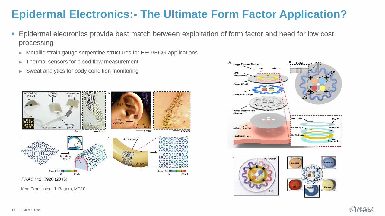
Epidermal Electronics:- The Ultimate Form Factor Application?
Epidermal electronics provide best match between exploitation of form factor and need for low cost
processing
► Metallic strain gauge serpentine structures for EEG/ECG applications
► Thermal sensors for blood flow measurement
► Sweat analytics for body condition monitoring
13
Kind Permission: J. Rogers, MC10
| External Use
Key R2R Processing Technology for the IoT,
Wearables & Wide Colour Gamut Displays
| External Use
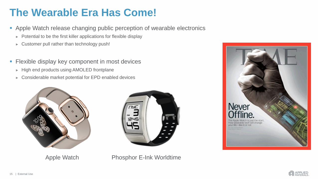
The Wearable Era Has Come!
Apple Watch release changing public perception of wearable electronics
► Potential to be the first killer applications for flexible display
► Customer pull rather than technology push!
Flexible display key component in most devices
► High end products using AMOLED frontplane
► Considerable market potential for EPD enabled devices
15
Apple Watch Phosphor E-Ink Worldtime
| External Use
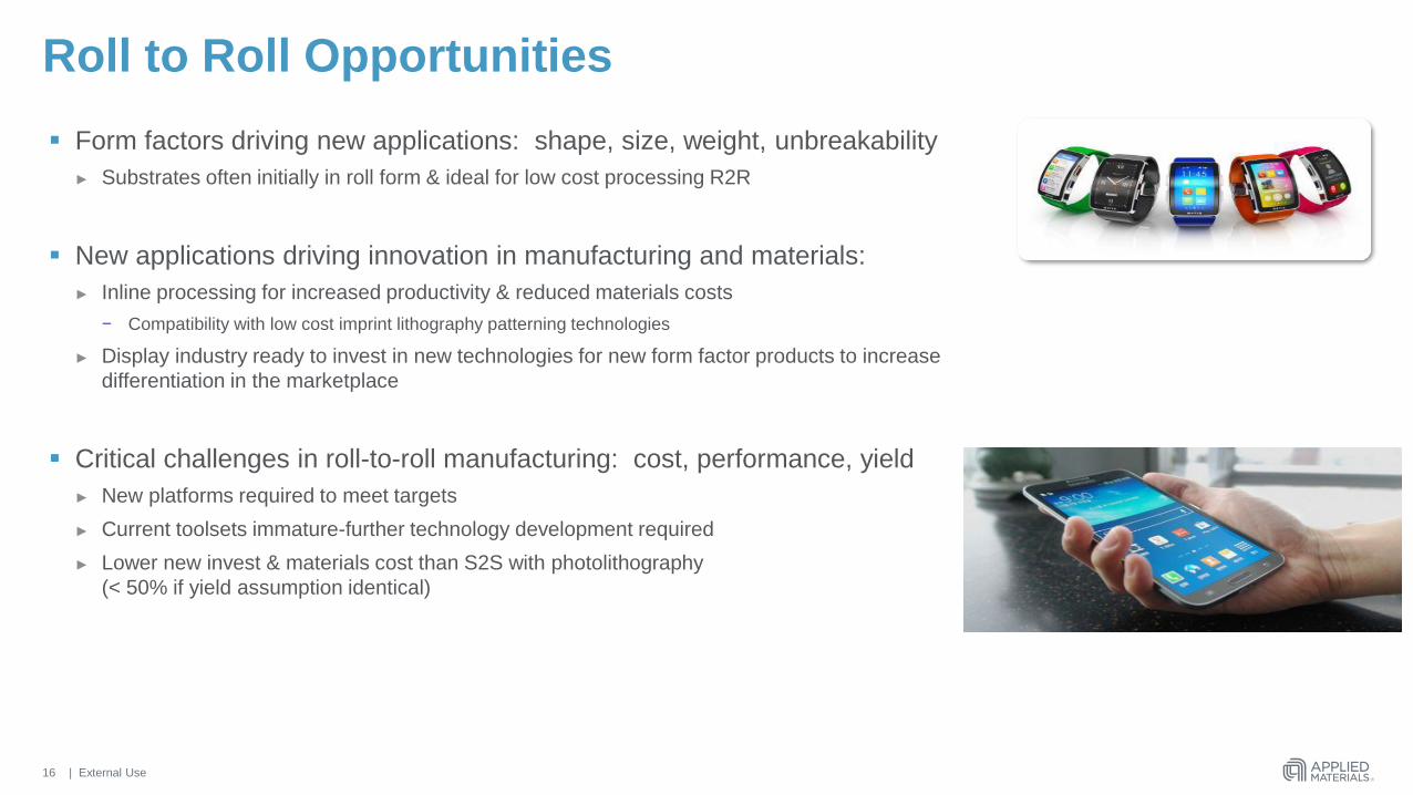
Roll to Roll Opportunities
Form factors driving new applications: shape, size, weight, unbreakability
► Substrates often initially in roll form & ideal for low cost processing R2R
New applications driving innovation in manufacturing and materials:
► Inline processing for increased productivity & reduced materials costs
− Compatibility with low cost imprint lithography patterning technologies
► Display industry ready to invest in new technologies for new form factor products to increase
differentiation in the marketplace
Critical challenges in roll-to-roll manufacturing: cost, performance, yield
► New platforms required to meet targets
► Current toolsets immature-further technology development required
► Lower new invest & materials cost than S2S with photolithography
(< 50% if yield assumption identical)
16
| External Use
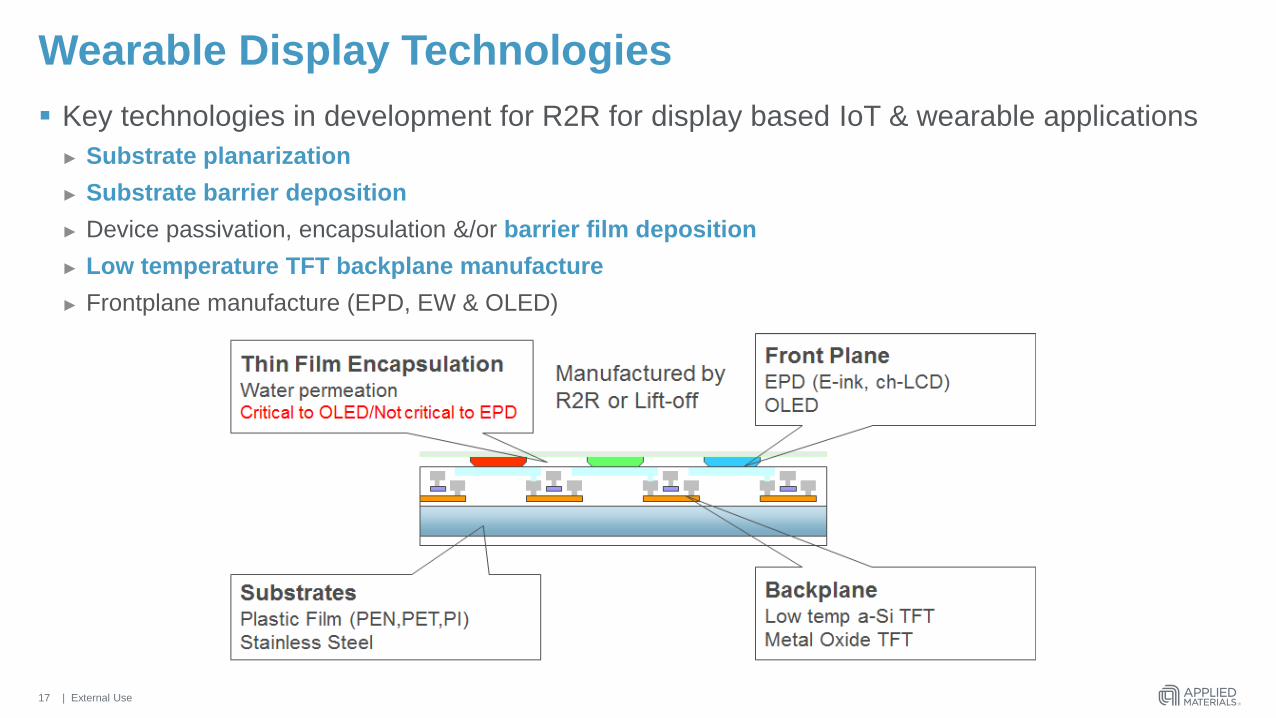
Wearable Display Technologies
Key technologies in development for R2R for display based IoT & wearable applications
► Substrate planarization
► Substrate barrier deposition
► Device passivation, encapsulation &/or barrier film deposition
► Low temperature TFT backplane manufacture
► Frontplane manufacture (EPD, EW & OLED)
17
| External Use
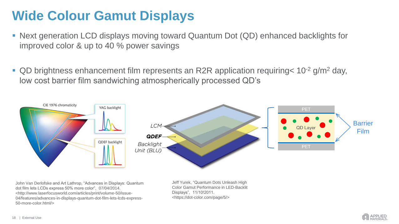
Wide Colour Gamut Displays
Next generation LCD displays moving toward Quantum Dot (QD) enhanced backlights for
improved color & up to 40 % power savings
QD brightness enhancement film represents an R2R application requiring< 10-2 g/m2 day,
low cost barrier film sandwiching atmospherically processed QD’s
Barrier
Film
18
Jeff Yurek, “Quantum Dots Unleash High
Color Gamut Performance in LED-Backlit
Displays”, 11/10!2011.
<https://dot-color.com/page/5/>
John Van Derlofske and Art Lathrop, “Advances in Displays: Quantum
dot film lets LCDs express 50% more color”, 07/04/2014.
<http://www.laserfocusworld.com/articles/print/volume-50/issue-
04/features/advances-in-displays-quantum-dot-film-lets-lcds-express-
50-more-color.html/>
| External Use
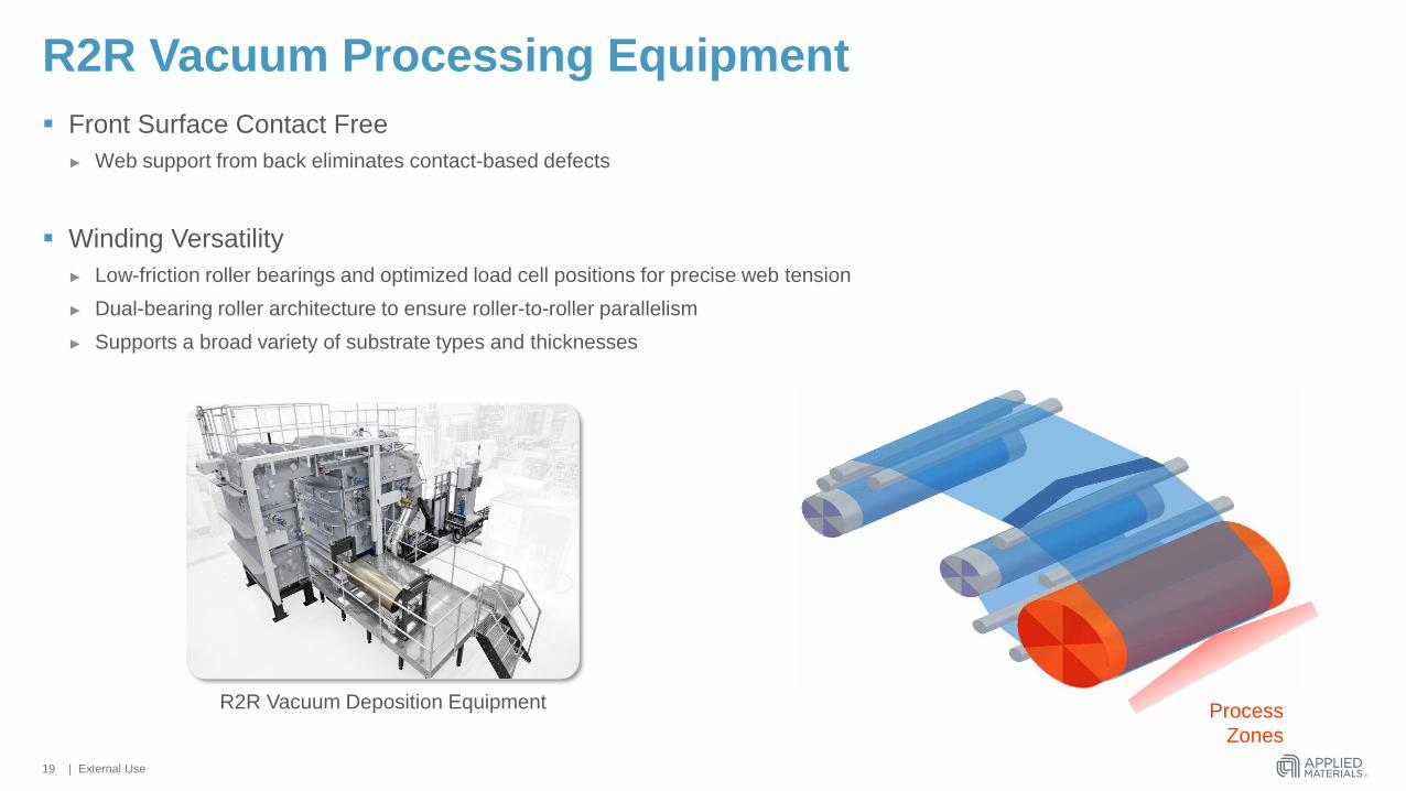
R2R Vacuum Processing Equipment
Front Surface Contact Free
► Web support from back eliminates contact-based defects
Winding Versatility
► Low-friction roller bearings and optimized load cell positions for precise web tension
► Dual-bearing roller architecture to ensure roller-to-roller parallelism
► Supports a broad variety of substrate types and thicknesses
19
Process
Zones
R2R Vacuum Deposition Equipment
| External Use
0
0,2
0,4
0,6
0,8
1
1,2
1,4
0 400 800 1200 1600
Web Width (mm)
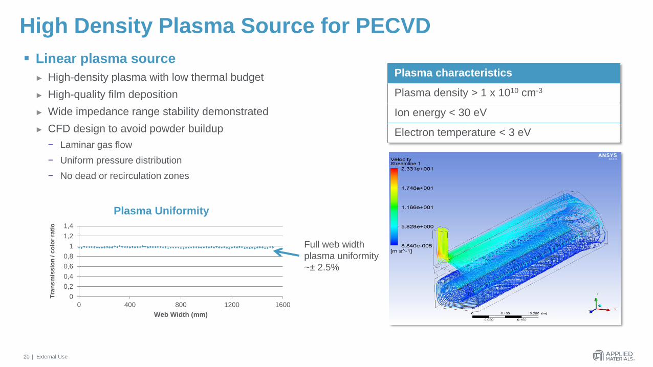
High Density Plasma Source for PECVD
Linear plasma source
► High-density plasma with low thermal budget
► High-quality film deposition
► Wide impedance range stability demonstrated
► CFD design to avoid powder buildup
− Laminar gas flow
− Uniform pressure distribution
− No dead or recirculation zones
Plasma characteristics
Plasma density > 1 x 1010 cm-3
Ion energy < 30 eV
Electron temperature < 3 eV
Plasma Uniformity
Full web width
plasma uniformity
~± 2.5%
Tra
ns
mis
sio
n / c
olo
r ra
tio
20
| External Use
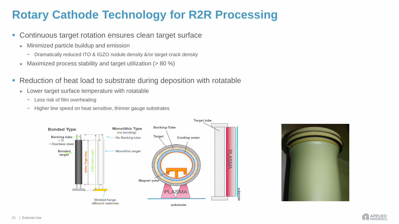
Rotary Cathode Technology for R2R Processing
Continuous target rotation ensures clean target surface
► Minimized particle buildup and emission
− Dramatically reduced ITO & IGZO nodule density &/or target crack density
► Maximized process stability and target utilization (> 80 %)
Reduction of heat load to substrate during deposition with rotatable
► Lower target surface temperature with rotatable
− Less risk of film overheating
− Higher line speed on heat sensitive, thinner gauge substrates
21
| External Use
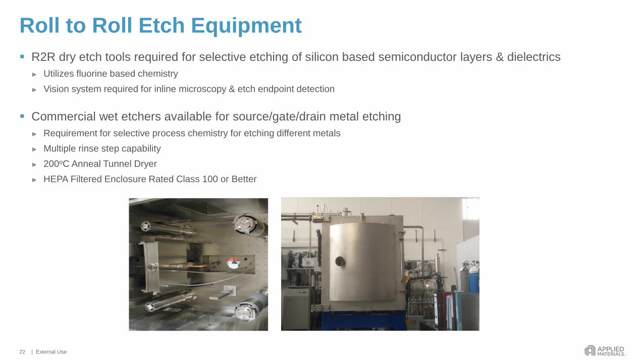
Roll to Roll Etch Equipment
R2R dry etch tools required for selective etching of silicon based semiconductor layers & dielectrics
► Utilizes fluorine based chemistry
► Vision system required for inline microscopy & etch endpoint detection
Commercial wet etchers available for source/gate/drain metal etching
► Requirement for selective process chemistry for etching different metals
► Multiple rinse step capability
► 200oC Anneal Tunnel Dryer
► HEPA Filtered Enclosure Rated Class 100 or Better
22
| External Use
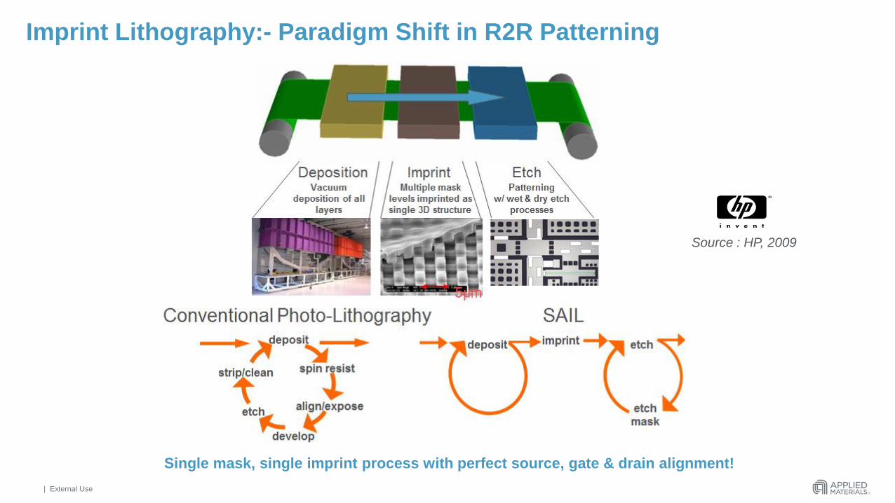
Imprint Lithography:- Paradigm Shift in R2R Patterning
Source : HP, 2009
Single mask, single imprint process with perfect source, gate & drain alignment!
| External Use
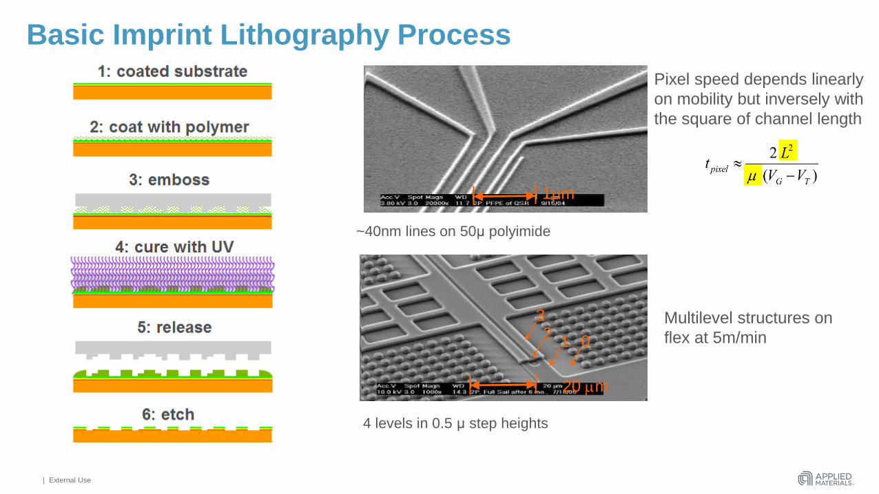
Basic Imprint Lithography Process
~40nm lines on 50μ polyimide
Multilevel structures on
flex at 5m/min
1μm
4 levels in 0.5 μ step heights
20 m
012
3
Pixel speed depends linearly
on mobility but inversely with
the square of channel length
| External Use
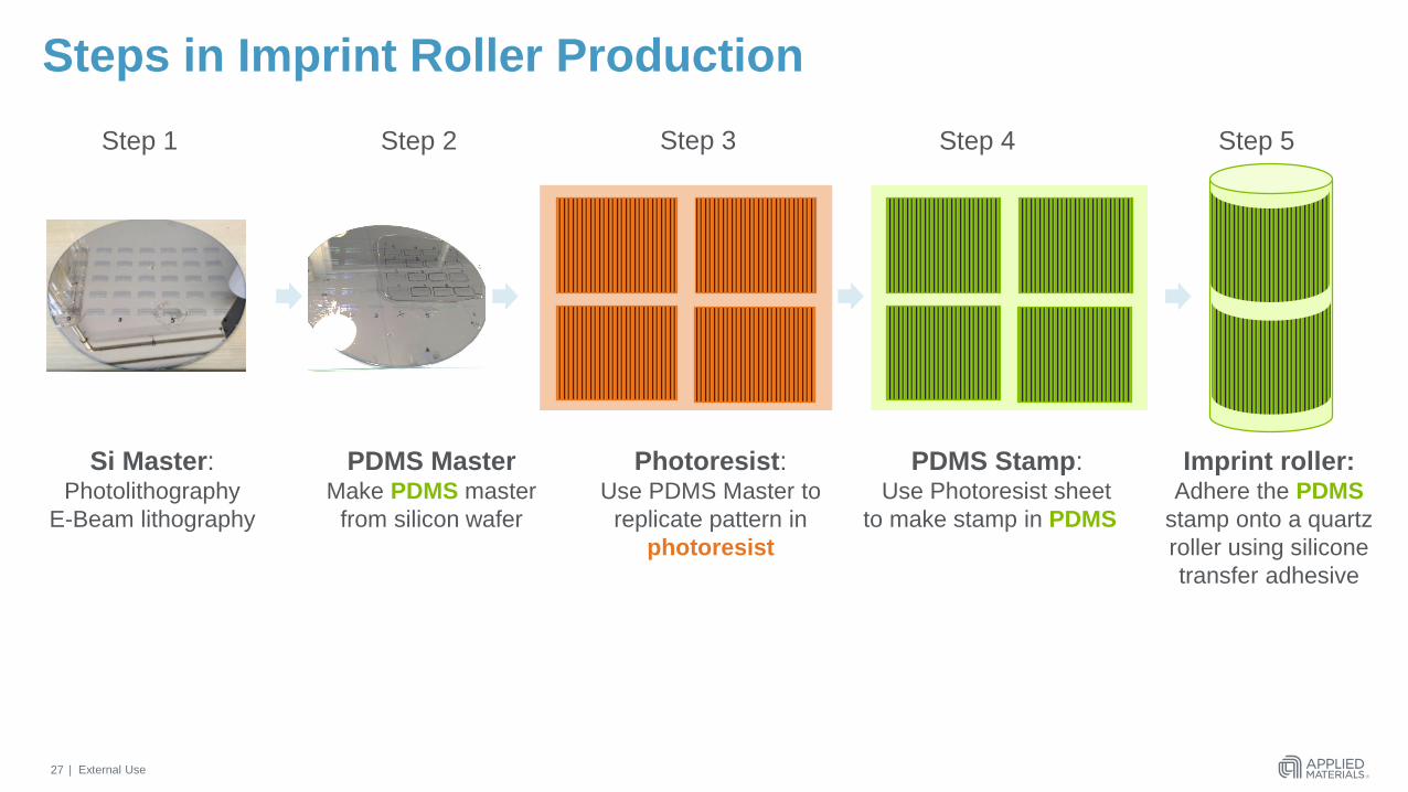
Steps in Imprint Roller Production
25
Step 1 Step 2 Step 3 Step 4 Step 5
Si Master:Photolithography
E-Beam lithography
PDMS MasterMake PDMS master
from silicon wafer
Photoresist:Use PDMS Master to
replicate pattern in
photoresist
PDMS Stamp:Use Photoresist sheet
to make stamp in PDMS
Imprint roller: Adhere the PDMS
stamp onto a quartz
roller using silicone
transfer adhesive
| External Use
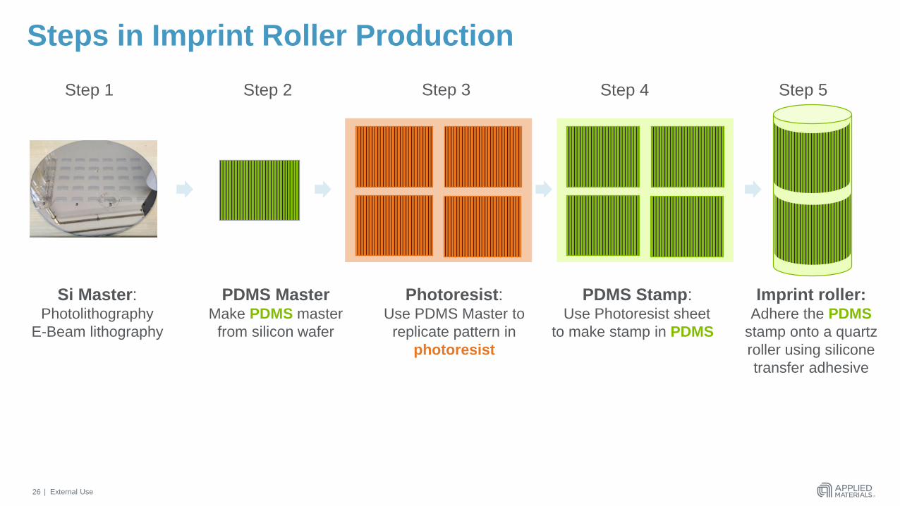
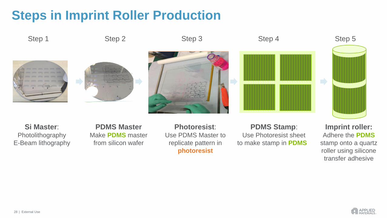
Steps in Imprint Roller Production
26
Step 1 Step 2 Step 3 Step 4 Step 5
Si Master:Photolithography
E-Beam lithography
PDMS MasterMake PDMS master
from silicon wafer
Photoresist:Use PDMS Master to
replicate pattern in
photoresist
PDMS Stamp:Use Photoresist sheet
to make stamp in PDMS
Imprint roller: Adhere the PDMS
stamp onto a quartz
roller using silicone
transfer adhesive
| External Use
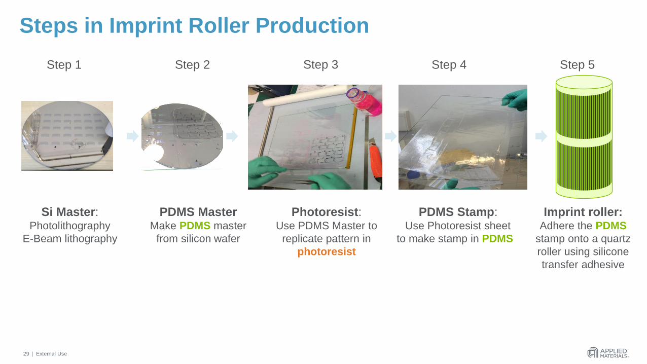
Steps in Imprint Roller Production
27
Step 1 Step 2 Step 3 Step 4 Step 5
Si Master:Photolithography
E-Beam lithography
PDMS MasterMake PDMS master
from silicon wafer
Photoresist:Use PDMS Master to
replicate pattern in
photoresist
PDMS Stamp:Use Photoresist sheet
to make stamp in PDMS
Imprint roller: Adhere the PDMS
stamp onto a quartz
roller using silicone
transfer adhesive
| External Use
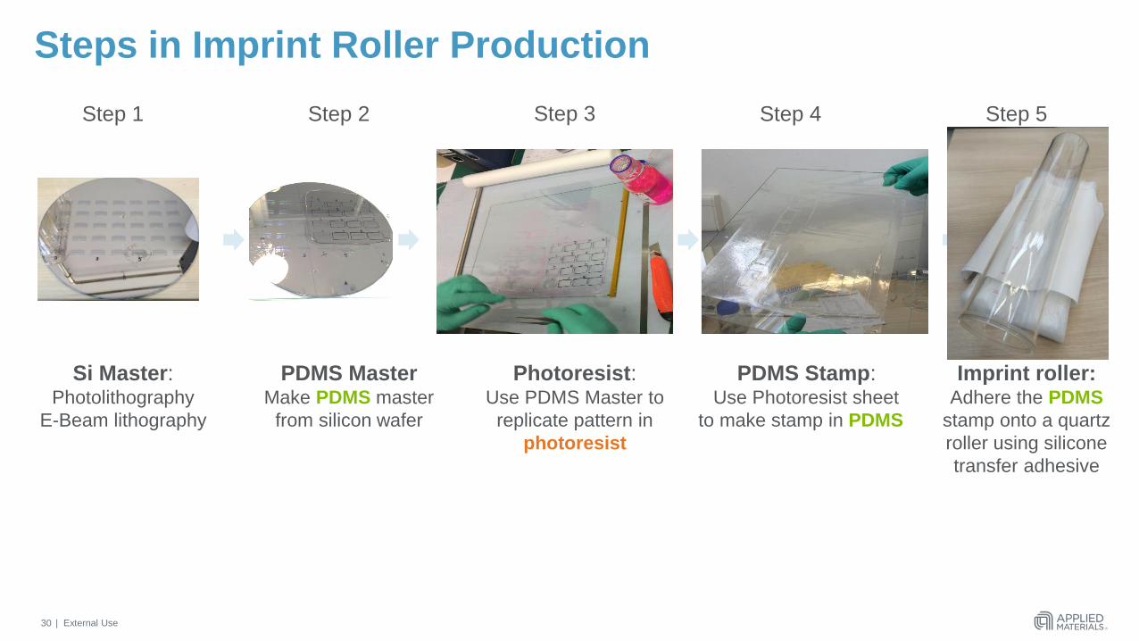
Steps in Imprint Roller Production
28
Step 1 Step 2 Step 3 Step 4 Step 5
Si Master:Photolithography
E-Beam lithography
PDMS MasterMake PDMS master
from silicon wafer
Photoresist:Use PDMS Master to
replicate pattern in
photoresist
PDMS Stamp:Use Photoresist sheet
to make stamp in PDMS
Imprint roller: Adhere the PDMS
stamp onto a quartz
roller using silicone
transfer adhesive
| External Use
Steps in Imprint Roller Production
29
Step 1 Step 2 Step 3 Step 4 Step 5
Si Master:Photolithography
E-Beam lithography
PDMS MasterMake PDMS master
from silicon wafer
Photoresist:Use PDMS Master to
replicate pattern in
photoresist
PDMS Stamp:Use Photoresist sheet
to make stamp in PDMS
Imprint roller: Adhere the PDMS
stamp onto a quartz
roller using silicone
transfer adhesive
| External Use
Steps in Imprint Roller Production
30
Step 1 Step 2 Step 3 Step 4 Step 5
Si Master:Photolithography
E-Beam lithography
PDMS MasterMake PDMS master
from silicon wafer
Photoresist:Use PDMS Master to
replicate pattern in
photoresist
PDMS Stamp:Use Photoresist sheet
to make stamp in PDMS
Imprint roller: Adhere the PDMS
stamp onto a quartz
roller using silicone
transfer adhesive
| External Use
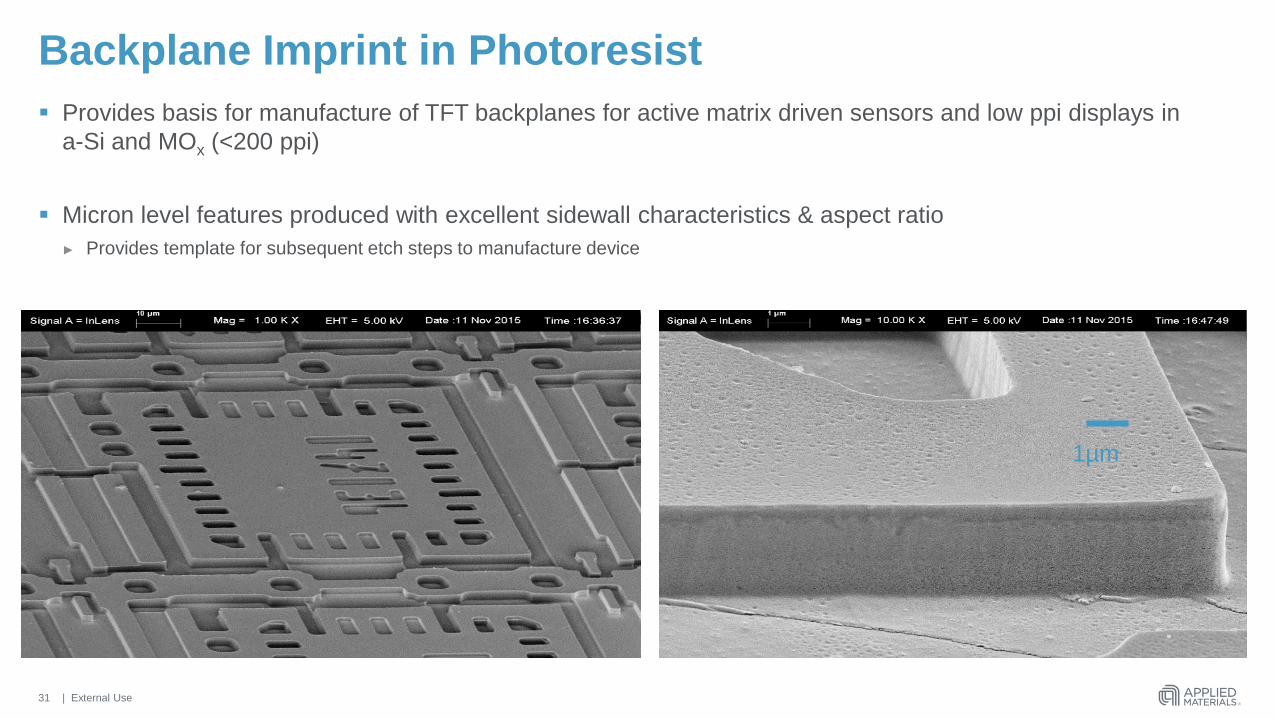
Backplane Imprint in Photoresist
Provides basis for manufacture of TFT backplanes for active matrix driven sensors and low ppi displays in
a-Si and MOx (<200 ppi)
Micron level features produced with excellent sidewall characteristics & aspect ratio
► Provides template for subsequent etch steps to manufacture device
31
1µm
| External Use
R2R Barrier & Thin Film Transistor
Processing
| External Use
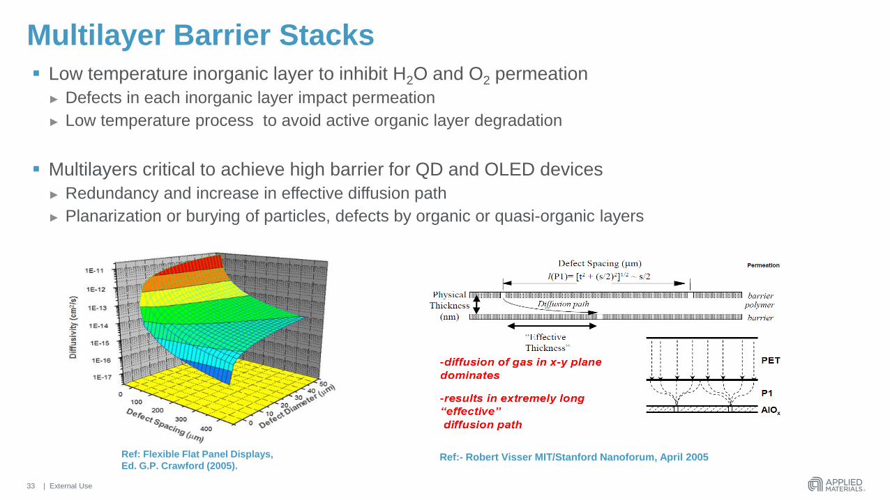
Multilayer Barrier Stacks
Low temperature inorganic layer to inhibit H2O and O2 permeation
► Defects in each inorganic layer impact permeation
► Low temperature process to avoid active organic layer degradation
Multilayers critical to achieve high barrier for QD and OLED devices
► Redundancy and increase in effective diffusion path
► Planarization or burying of particles, defects by organic or quasi-organic layers
33
Ref:- Robert Visser MIT/Stanford Nanoforum, April 2005Ref: Flexible Flat Panel Displays,
Ed. G.P. Crawford (2005).
| External Use
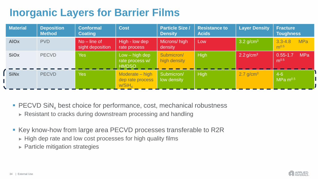
Inorganic Layers for Barrier Films
PECVD SiNx best choice for performance, cost, mechanical robustness
► Resistant to cracks during downstream processing and handling
Key know-how from large area PECVD processes transferable to R2R
► High dep rate and low cost processes for high quality films
► Particle mitigation strategies
34
Material Deposition
Method
Conformal
Coating
Cost Particle Size /
Density
Resistance to
Acids
Layer Density Fracture
Toughness
AlOx PVD No – line of
sight deposition
High - low dep
rate process
Microns/ high
density
Low 3.2 g/cm3 3.3-4.8 MPa
m0.5
SiOx PECVD Yes Low – high dep
rate process w/
HMDSO
Submicron/
high density
High 2.2 g/cm3 0.55-1.7 MPa
m0.5
SiNx PECVD Yes Moderate – high
dep rate process
w/SiH4
Submicron/
low density
High 2.7 g/cm3 4-6
MPa m0.5
| External Use
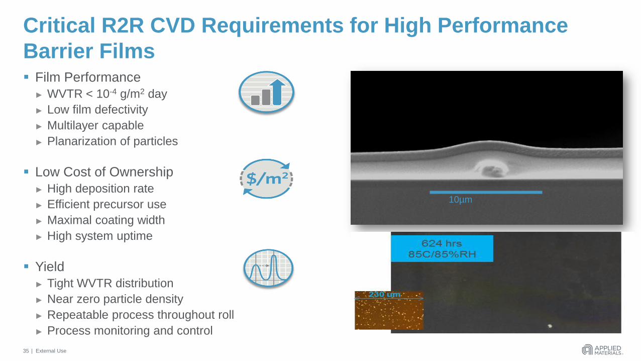
Film Performance
► WVTR < 10-4 g/m2 day
► Low film defectivity
► Multilayer capable
► Planarization of particles
Low Cost of Ownership
► High deposition rate
► Efficient precursor use
► Maximal coating width
► High system uptime
Yield
► Tight WVTR distribution
► Near zero particle density
► Repeatable process throughout roll
► Process monitoring and control
Critical R2R CVD Requirements for High Performance
Barrier Films
10µm
35
| External Use
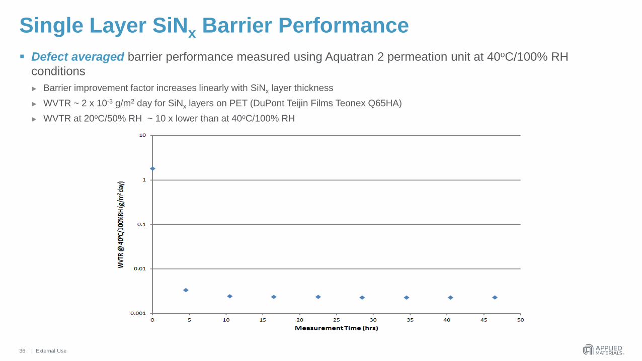
Single Layer SiNx Barrier Performance
Defect averaged barrier performance measured using Aquatran 2 permeation unit at 40oC/100% RH
conditions
► Barrier improvement factor increases linearly with SiNx layer thickness
► WVTR ~ 2 x 10⁻³ g/m2 day for SiNx layers on PET (DuPont Teijin Films Teonex Q65HA)
► WVTR at 20oC/50% RH ~ 10 x lower than at 40oC/100% RH
36
| External Use
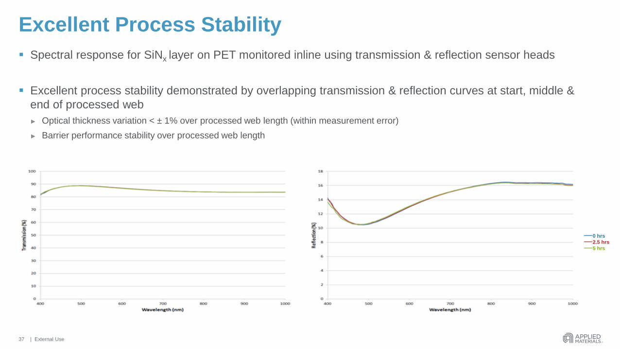
Excellent Process Stability
Spectral response for SiNx layer on PET monitored inline using transmission & reflection sensor heads
Excellent process stability demonstrated by overlapping transmission & reflection curves at start, middle &
end of processed web
► Optical thickness variation < ± 1% over processed web length (within measurement error)
► Barrier performance stability over processed web length
37
0 hrs
2.5 hrs
5 hrs
| External Use
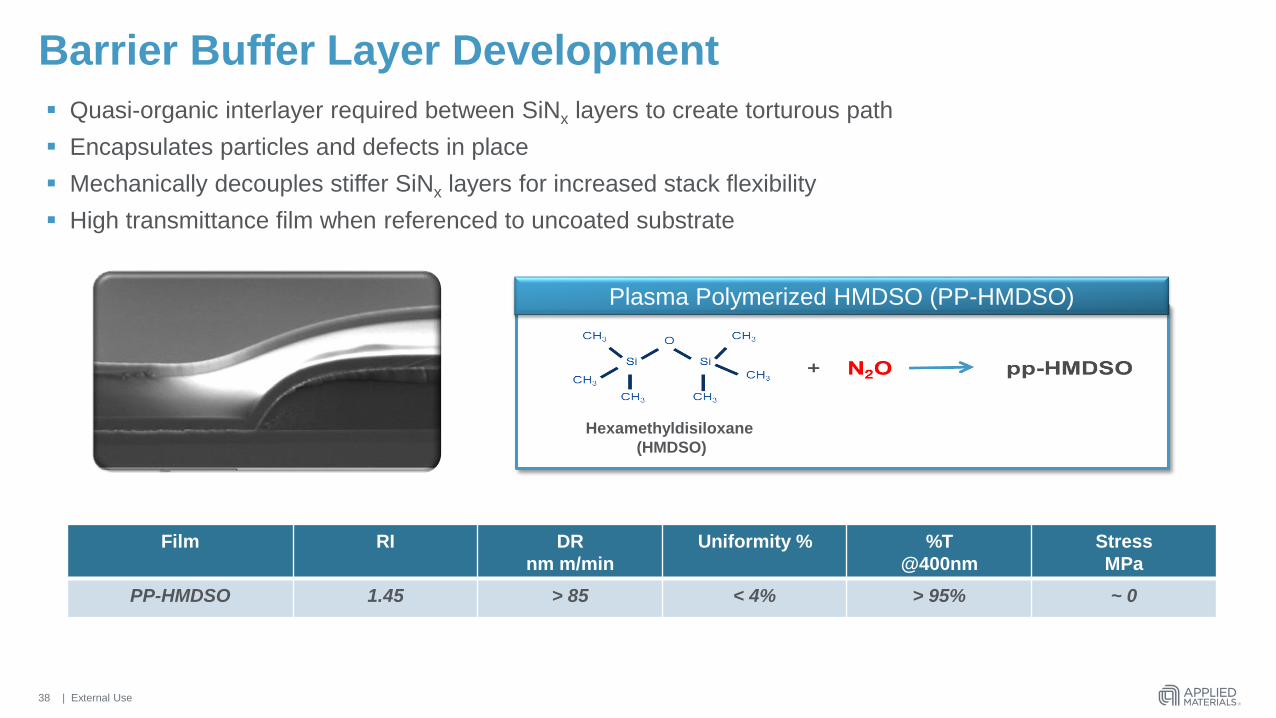
Barrier Buffer Layer Development
Quasi-organic interlayer required between SiNx layers to create torturous path
Encapsulates particles and defects in place
Mechanically decouples stiffer SiNx layers for increased stack flexibility
High transmittance film when referenced to uncoated substrate
38
Film RI DR
nm m/min
Uniformity % %T
@400nm
Stress
MPa
PP-HMDSO 1.45 > 85 < 4% > 95% ~ 0
Plasma Polymerized HMDSO (PP-HMDSO)
Hexamethyldisiloxane
(HMDSO)
| External Use
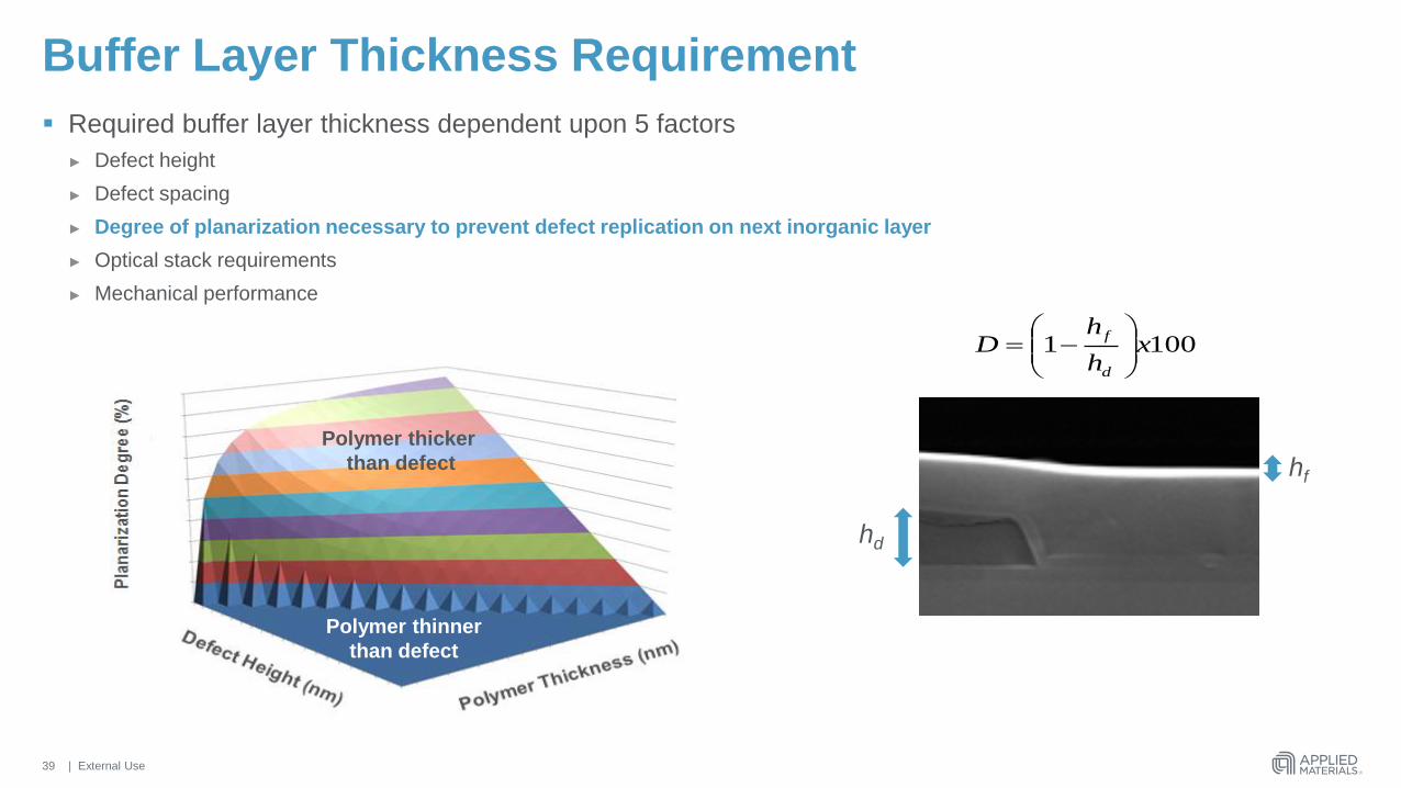
Buffer Layer Thickness Requirement
Required buffer layer thickness dependent upon 5 factors
► Defect height
► Defect spacing
► Degree of planarization necessary to prevent defect replication on next inorganic layer
► Optical stack requirements
► Mechanical performance
39
1001 xh
hD
d
f
hf
hd
Polymer thicker
than defect
Polymer thinner
than defect
| External Use
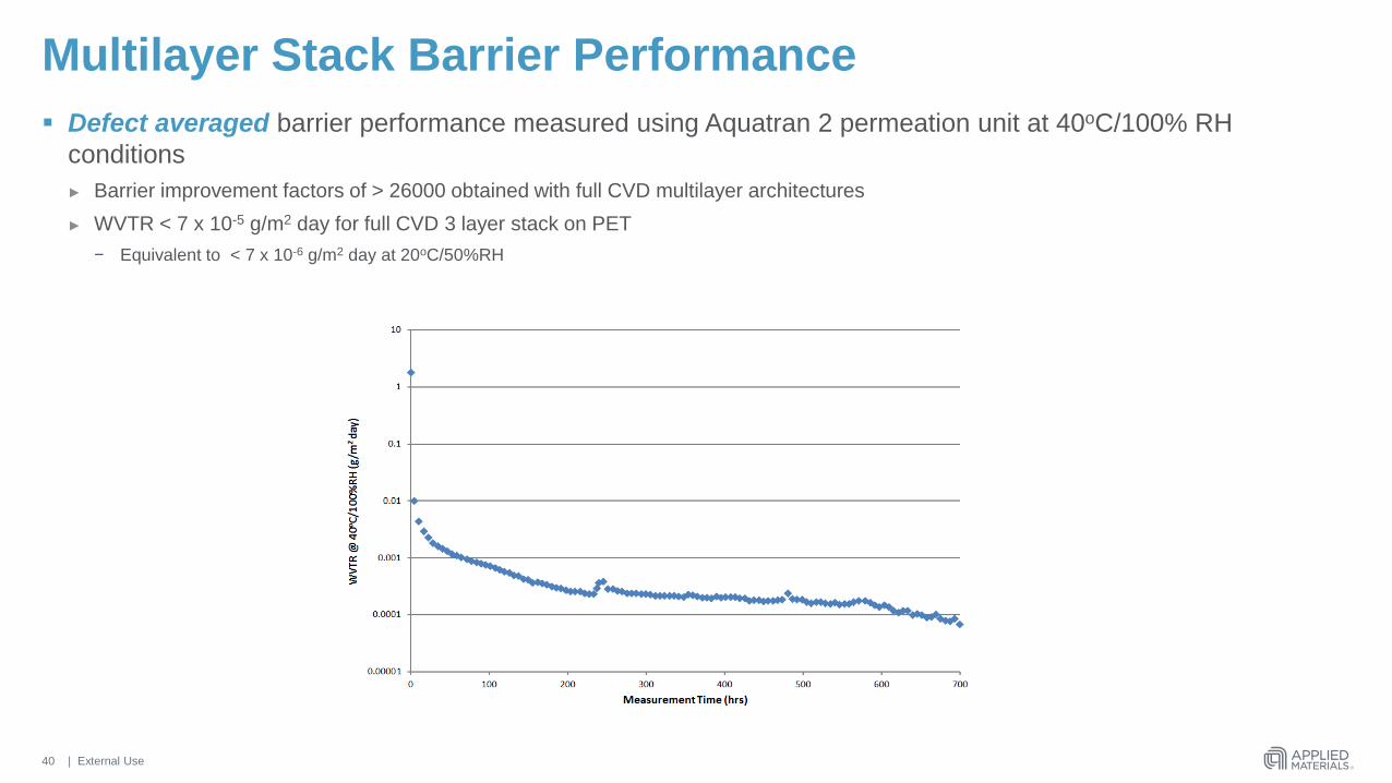
Multilayer Stack Barrier Performance
Defect averaged barrier performance measured using Aquatran 2 permeation unit at 40oC/100% RH
conditions
► Barrier improvement factors of > 26000 obtained with full CVD multilayer architectures
► WVTR < 7 x 10⁻⁵ g/m2 day for full CVD 3 layer stack on PET
− Equivalent to < 7 x 10⁻⁶ g/m2 day at 20oC/50%RH
40
| External Use
R2R Process Flow: a-Si:H Devices
High grade, low surface roughness 50 m PI foil used
► Bakeout required for mechanical stabilization & outgassing
► Foil plasma pretreated to enhance layer stack adhesion
► Deposition of barrier layer stack in CVD lab tool
TFT layer stack deposition
► Al Gate metal layer deposited in PVD tool
► SiO2 etch stop layer, SiNx gate dielectric, aSi channel layer & n+ contact layer deposited in CVD tool
► Cr source/drain metal layer deposited in PVD tool
Device patterning
► Imprint lithography used to pattern stack in single step
− Coplanar device architecture
► Dry/wet etch steps used to provide final device structure
41
| External Use
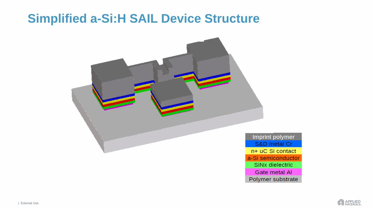
Simplified a-Si:H SAIL Device Structure
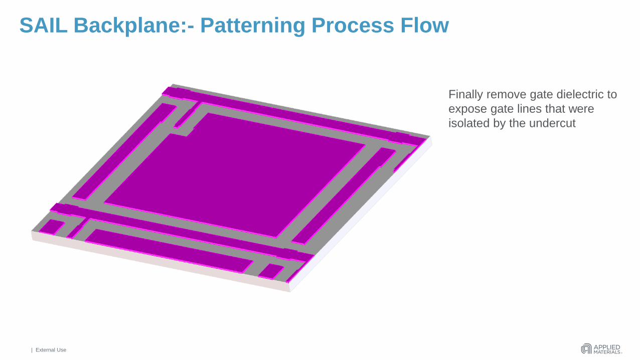
| External Use
Imprint mask on TFT stack
consisting of
•Top metal
•Contact layer (optional)
•Semiconductor
•Dielectric
•Bottom metal
Process produces complete
backplane:
TFT
Pixel electrode
Data line
Crossover
Gate line
Etch exposed stack all the way
to the substrate undercutting the
bottom metal in the thin regions
to isolate the gate lines and the
TFTs
Etch the polymer down to
expose the layers covering
the gate lines
Etch through top metal and
(optionally) other layers to
form crossovers
Etch polymer a second time to
expose area covering TFT
channel
Etch top metal and contact layer to
define TFT channel
Remove remaining polymer to
expose completed backplane
Disassemble array one layer at a
time to expose structure. Begin by
removing top metal
Next remove contact layer to
expose channel semiconductor
Then remove semiconductor to
expose gate dielectricFinally remove gate dielectric to
expose gate lines that were
isolated by the undercut
SAIL Backplane:- Patterning Process Flow
| External Use
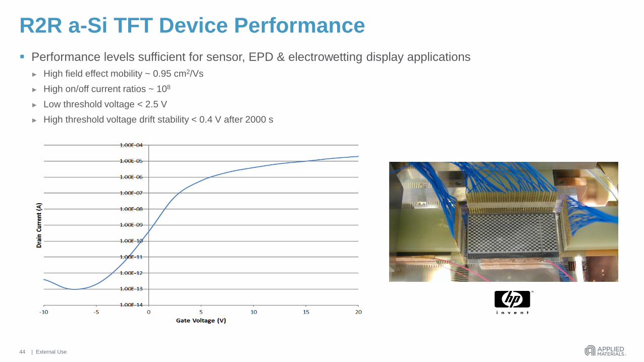
R2R a-Si TFT Device Performance
Performance levels sufficient for sensor, EPD & electrowetting display applications
► High field effect mobility ~ 0.95 cm2/Vs
► High on/off current ratios ~ 108
► Low threshold voltage < 2.5 V
► High threshold voltage drift stability < 0.4 V after 2000 s
44
| External Use
Hybrid Approaches to Manufacturing
| External Use
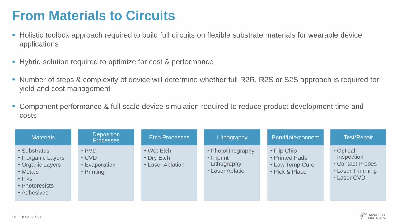
From Materials to Circuits
Holistic toolbox approach required to build full circuits on flexible substrate materials for wearable device
applications
Hybrid solution required to optimize for cost & performance
Number of steps & complexity of device will determine whether full R2R, R2S or S2S approach is required for
yield and cost management
Component performance & full scale device simulation required to reduce product development time and
costs
46
Materials
• Substrates
• Inorganic Layers
• Organic Layers
• Metals
• Inks
• Photoresists
• Adhesives
Deposition Processes
• PVD
• CVD
• Evaporation
• Printing
Etch Processes
• Wet Etch
• Dry Etch
• Laser Ablation
Lithography
• Photolithography
• Imprint Lithography
• Laser Ablation
Bond/Interconnect
• Flip Chip
• Printed Pads
• Low Temp Cure
• Pick & Place
Test/Repair
• Optical Inspection
• Contact Probes
• Laser Trimming
• Laser CVD
| External Use
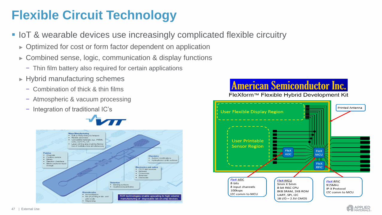
Flexible Circuit Technology
IoT & wearable devices use increasingly complicated flexible circuitry
► Optimized for cost or form factor dependent on application
► Combined sense, logic, communication & display functions
− Thin film battery also required for certain applications
► Hybrid manufacturing schemes
− Combination of thick & thin films
− Atmospheric & vacuum processing
− Integration of traditional IC’s
47
| External Use
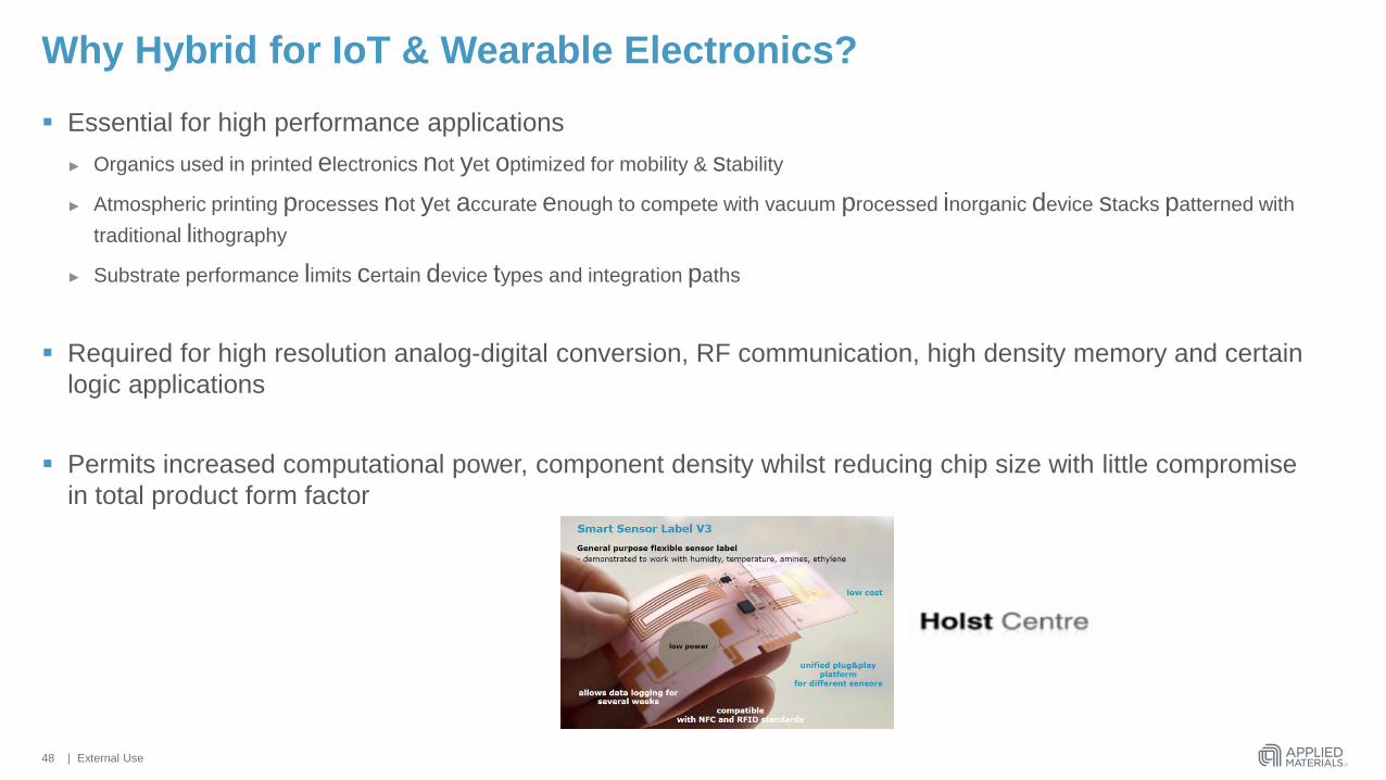
Why Hybrid for IoT & Wearable Electronics?
Essential for high performance applications
► Organics used in printed electronics not yet optimized for mobility & stability
► Atmospheric printing processes not yet accurate enough to compete with vacuum processed inorganic device stacks patterned with
traditional lithography
► Substrate performance limits certain device types and integration paths
Required for high resolution analog-digital conversion, RF communication, high density memory and certain
logic applications
Permits increased computational power, component density whilst reducing chip size with little compromise
in total product form factor
48
| External Use
Summary
| External Use50
| External Use51
Summary
The IoT & wearable era has arrived!
► Explosion in products announced on the market in 2014/2015
► Products incorporating display, communication and sense capabilities leading “consumer” adoption
− Pebble & Apple Watch paving the way for broader range of wearable fashion lead devices
Display based applications show largest growth potential for vacuum processing of inorganic layers on
flexible substrates for electronics
► R2R already in high volume manufacturing for transparent materials in Touch Panel
► Pilot line demonstration of R2R manufacture of complex device architectures including flexible TFT backplanes
Hybrid integration schemes required to combine the advantages of traditional silicon IC logic & memory
capability with large scale integrated sensor and display devices
Applied Materials driving to lowest cost/m2 at highest performance
through equipment design, scaling, metrology and yield strategies