Embed Size (px)
Citation preview
VP = 0— VP = VDD
L — C
Vout
VN I G 4FET VPNDR
VDD
0 0.5 1.0 1.5 2.0 2.5 3.0 3.5
Vin, Volts
formance — specifically, gain and phase(see figure). The automated test systemuses the LabVIEW software to controlthe test equipment, collect the data, andwrite it to a file. The input to the Lab -VIEW program is either user-input forsystematic variation, or is provided in afile containing specific test values thatshould be fed to the VMLTT. The outputfile contains both the control signals andthe measured data.
The second step is to post-process thefile to determine the correction functionsas needed. The result of the entireprocess is a tabular representation, whichallows translation of a desired I/Q valueto the required analog control signals toproduce a particular RF behavior. Insome applications, “corrected” perform-
ance is needed only for a limited range. Ifthe vector modulator is being used as aphase shifter, there is only a need to cor-rect I and Q values that represent pointson a circle, not the entire plane.
This innovation has been used to cali-brate 2-GHz MMIC (monolithic micro -wave integrated circuit) vector modula-tors in the High EIRP Cluster Arrayproject (EIRP is high effective isotropicradiated power). These calibrationswere then used to create correction ta-bles to allow the commanding of thephase shift in each of four channels usedas a phased array for beam steering of aKa-band (32-GHz) signal.
The system also was the basis of abreadboard electronic beam steeringsystem. In this breadboard, the goal was
not to make systematic measurements ofthe properties of a vector modulator, butto drive the breadboard with a series oftest patterns varying in phase and ampli-tude. This is essentially the same calibra-tion process, but with the difference thatthe data collection process is orientedtoward collecting breadboard perform-ance, rather than the measurement ofoutput from a network analyzer.
This work was done by James Lux, AmyBoas, and Samuel Li of Caltech for NASA’s , jetPropulsion Laboratory. Further information iscontained in a TSP (see page 1).
The software used in this innovation isavailable for commercial licensing. Pleasecontact Karina Edmonds of the California In-stitute of Technology at (626) 395-2322.Refer to NPO-44518.
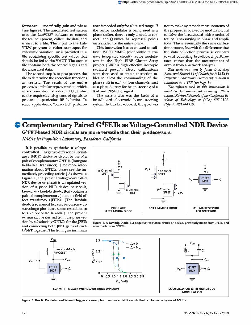
r Complementary Paired G4FETs as Voltage-Controlled NDR DeviceG4FET-based NDR circuits are more versatile than their predecessors.NASA’s , jet Propulsion Laboratory, Pasadena, California
It is possible to synthesize a voltage-controlled negative-differential-resist-ance (NDR) device or circuit by use of apair of complementary G 4FETs (four-gatefield-effect transistors). [For more infor-mation about G4FETs, please see the im-mediately preceding article.] As shown inFigure 1, the present voltage-controlledNDR device or circuit is an updated ver-sion of a prior NDR device or circuit,known as a lambda diode, that contains apair of complementary junction field-ef-fect transistors (JFETs). (The lambdadiode is so named because its current-ver-sus-voltage plot bears some resemblanceto an upper-case lambda.) The presentversion can be derived from the prior ver-sion by substituting G4FETs for the JFETsand connecting both JFET gates of eachG4FET together. The front gate terminals
V
IV
IV
n-ChannelVNed n-Channel I
JFET G4FET
VN —1G 4FET VP
NDR
p-Channel p-Channel —JFET G4FET VP
PRIOR ART: G4FET LAMBDA DIODE SCHEMATIC SYMBOLJFET LAMBDA DIODE FOR G4FET NDR
Figure 1. A Lambda Diode is a negative-resistance circuit or device, previously made from JFETs, andnow made from G4FETs.
VDD 3.3
Inversion-ModePMOSFET o 2.2
VoutV'n
o'1.1
G 4FET VNDR P
0
SCHMITT TRIGGER WITH ADJUSTABLE WINDOW
LC OSCILLATOR WITH AMPLITUDEMODULATION
Figure 2. This LC Oscillator and Schmitt Trigger are examples of enhanced NDR circuits that can be made by use of G 4FETs.
12 NASA Tech Briefs, October 2009
https://ntrs.nasa.gov/search.jsp?R=20090035906 2018-02-16T17:28:24+00:00Z

of the G4FETs constitute additional termi-nals (that is, terminals not available in theolder JFET version) to which one canapply control voltages VN and VP .
Circuits in which NDR devices havebeen used include (1) Schmitt triggersand (2) oscillators containing induc-tance/capacitance (LC) resonant cir-cuits. Figure 2 depicts such circuits con-taining G4FET NDR devices like that ofFigure 1. In the Schmitt trigger shownhere, the G4FET NDR is loaded with anordinary inversion-mode, p-channel,metal oxide/semiconductor field-effecttransistor (inversion-mode PMOSFET),the VN terminal of the G4FET NDR de-vice is used as an input terminal, and theinput terminals of the PMOSFET andthe G4FET NDR device are connected.VP can be used as an extra control volt-
age (that is, a control voltage not avail-able in a typical prior Schmitt trigger)for adjusting the pinch-off voltage of thep-channel G4FET and thereby adjustingthe trigger-voltage window.
In the oscillator, a G4FET NDR deviceis loaded with a conventional LC tank cir-cuit. As in other LC NDR oscillators, oscil-lation occurs because the NDR counter-acts the resistance in the tank circuit. Theadvantage of this G4FET-NDR LC oscilla-tor over a conventional LC NDR oscilla-tor is that one can apply a time-varyingsignal to one of the extra control inputterminals ( VN or VP) to modulate the con-ductance of the NDR device and therebyamplitude-modulate the output signal.
This work was done by Mohammad Mojar-radi of Caltech; Suheng Chen, Ben Blalock,Chuck Britton, Ben Prothro, and , james Vander-
sand of the University of Tennessee; RonSchrimph of Vanderbilt University; and SorinCristoloveanu, Kerem Akarvardar, and P. Gen-til of Grenoble University for NASA’s , jet Propul-sion Laboratory. Further information is con-tained in a TSP (see page 1).
In accordance with Public Law 96-517,the contractor has elected to retain title to thisinvention. Inquiries concerning rights for itscommercial use should be addressed to:
Innovative Technology Assets ManagementJPLMail Stop 202-2334800 Oak Grove DrivePasadena, CA 91109-8099(818) 354-2240E-mail: [email protected] to NPO-43929, volume and number
of this NASA Tech Briefs issue, and thepage number.
Three MMIC Amplifiers for the 120-to-200 GHz Frequency BandThese would complement previously reported MMIC amplifiers designed for overlappingfrequency bands.NASA’s , jet Propulsion Laboratory, Pasadena, California
Closely following the developmentreported in the immediately preced-ing article, three new monolithic mi-crowave integrated circuit (MMIC)amplifiers that would operate in the120-to-200-GHz frequency band havebeen designed and are under con-struction at this writing. The active de-vices in these amplifiers are InP high-electron-mobility transistors (HEMTs).These amplifiers (see figure) are de-noted the LSLNA150, the LSA200,and the LSA185, respectively.
Like the amplifiers reported in theimmediately preceding article, theLSLNA150 (1) is intended to be aprototype of low-noise amplifiers(LNAs) to be incorporated intospaceborne instruments for sensingcosmic microwave background radia-tion and (2) has potential for terres-trial use in electronic test equipment,passive millimeter-wave imaging sys-tems, radar receivers, communica-tion receivers, and systems for detect-ing hidden weapons. The HEMTs inthis amplifier were fabricated accord-ing to 0.08-µm design rules of a com-mercial product line of InP HEMTMMICs at HRL Laboratories, LLC,with a gate geometry of 2 fingers,each 15 µm wide. On the basis ofcomputational simulations, this am-plifier is designed to afford at least 15
20 r r r r r15
10 /7-150
5 r r r*tttt^0
–5 t t t t t 1–10
7
^1y''
+ Ti
y
' ^Ty+
+ 1–15
–20 llTll ' iiT llTll 1
–25 T T T T T 1–30
80 100 120 140 160 180 200Frequency, GHz
10 f TTTYTTTTTT'0 fffff t rt t r 1
–10LSA200
13
–20
1 1 1 1 1.
–30
100 120 140 160 180 200 220Frequency, GHz
10 ]F TTTFFFFFFF
0 +tfftft^^, 4^_LSA185
^o Litt;–30
100 120 140 160 180 200 220Frequency, GHz
These Three MMIC Amplifiers have been designed to be suitable for a variety of applications at frequen-cies up to about 200 GHz.
NASA Tech Briefs, October 2009 13