Embed Size (px)
Citation preview

QuickLogic’sThe Basics of PCIQuickPCI - The PCI Solution for System Needs
Introducing… Introducing…

PCI 2
TypicalTypical SystemSystem ImplementationImplementation
CPU Cache MemorySubsystem
DRAM SubsystemPCI Bridge/Memory Controller
Host Bus
PCI Local Bus
PCI Add-in Slots
ISA BusBridge ISA Add-in Slots
ISA Bus

PCI 3
DesktopDesktop PlatformsPlatforms
Exp BusXface
Exp BusXface
IDEIDE
ProcessorProcessor
Bridge/Memory
Controller
Bridge/Memory
Controller DRAMDRAM
LAN, SCSI,Video, etc
GraphicsGraphics
PCI Local Bus
ISA/EISA - MicroChannel
CacheCache
Add-in
FaxModem
R
PCI 4
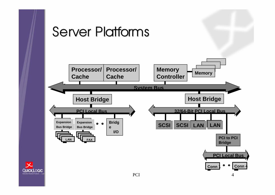
ServerServer PlatformsPlatforms
Expansion
Bus Bridge
Host Bridge
System Bus
Processor/Cache
Processor/Cache
MemoryController
Memory
Host Bridge
PCI to PCIBridge
LAN LANSCSI
Conn 1 Conn 4
PCI Local Bus 32/64-Bit PCI Local Bus
Expansion
Bus Bridge
LAN FAX
PCI Local Bus
Bridge
I/O
SCSI
PCI 5
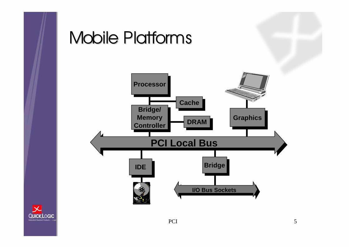
MobileMobile PlatformsPlatforms
IDEIDE
ProcessorProcessor
Bridge/Memory
Controller
Bridge/Memory
Controller DRAMDRAM GraphicsGraphics
PCI Local Bus
CacheCache
BridgeBridge
I/O Bus Sockets

PCI 6
PCI AutoPCI Auto--ConfigurationConfiguration
+PCIPCI AddAdd--in Cardin Card
PCIPCI Based MotherBased MotherBoardBoard AutoAuto ConfigurationConfiguration
SystemSystem

PCI 7
PCIPCI OverviewOverview

PCI 8
PCI FeaturesPCI Features
z 32-Bit or 64-Bit address and dataz 66 or 33 down to 0 MHz synchronous
operationz Single or multiple bus mastersz Reflected bus signaling z Stepped signalingz Bus parity error reportingz 5 or 3.3 volt operationz Cache supportz JTAG testing

PCI 9
PCI BusPCI Bus
z Bus Signalsz Bus Commandsz Bus Transactionsz Arbitration

PCI 10
RST
CLK
GNT#REQ#
IDSELDEVSEL#
STOP#IRDY#TRDY#
FRAME#
PAR
C/BE#[3::0]
AD[31::00]
TMSTCK
SDONE
SBO#
LOCK#
REQ64#ACK64#
PAR64
C/BE#[7::4]
AD[63::32]
TDO
TDI
TRST#
PCI Pin List
Required Pins Optional Pins
PCICOMPLIANT
DEVICE
64-BitExtension
InterfaceControl
CacheSupport
JTAG(IEEE 1149.1)
Address& Data
InterfaceControl
Arbitration(masters only)
System
SERR#PERR#Error
Reporting
Interrupt A-D#
Present 1-2
Clkrun#
M66EN
PCI Bus SignalsPCI Bus Signals
PCI 11
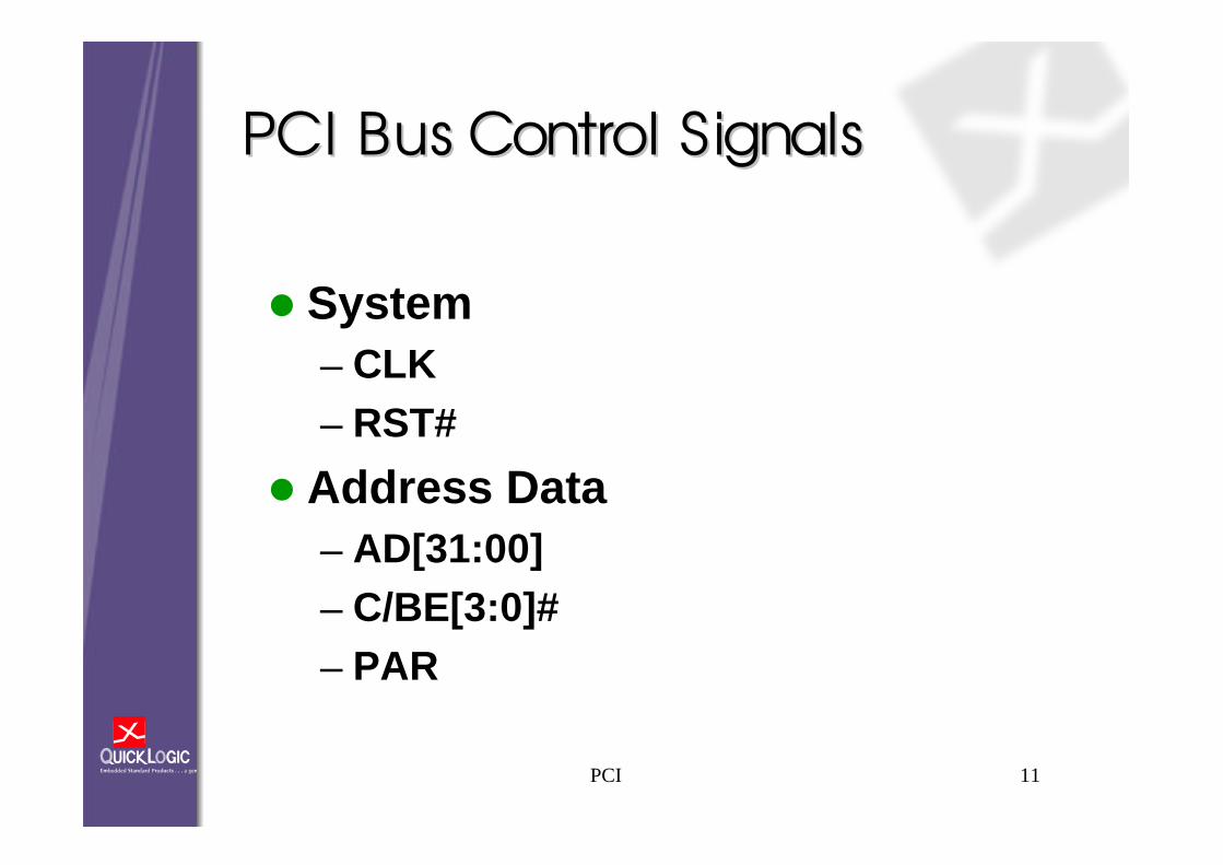
PCI BusPCI Bus ControlControl SignalsSignals
z System– CLK– RST#
z Address Data– AD[31:00]– C/BE[3:0]#– PAR

PCI 12
PCI BusPCI Bus ControlControl SignalsSignals
z Interface Control– FRAME# - LOCK#– IRDY# - IDSEL#– TRDY# - DEVSEL#– STOP#
z Arbitration– REQ#– GNT#

PCI 13
PCIPCI bus accessbus access
z PCI is a Multimaster Busz All transactions initiated by a
masterz All transactions to/from a target
PCI 14
PCI BusPCI Bus ControlControl SignalsSignals
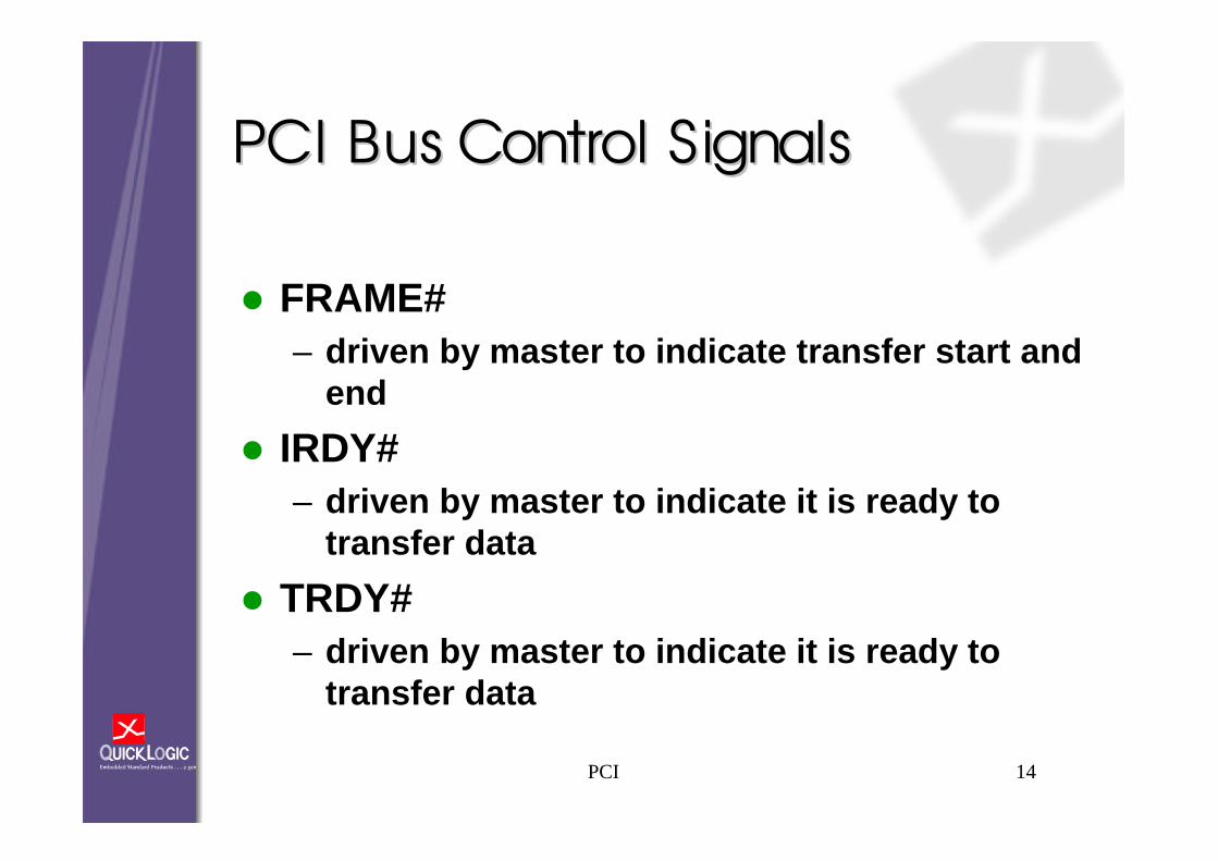
z FRAME#– driven by master to indicate transfer start and
end
z IRDY#– driven by master to indicate it is ready to
transfer data
z TRDY#– driven by master to indicate it is ready to
transfer data

PCI 15
Address
42 31 5 6 7 8CLK
9
FRAME#
AD
C/BE# Command
IRDY#
GNT#
Bus Idle
Bus transaction start

PCI 16
PCIPCI CommandCommand DefinitionDefinition
C/BE [3::0]# Command Type
0000 Interrupt acknowledge
0001 Special Cycle
0010 I/O Read
0011 I/O Write
0110 Memory Read
0111 Memory Write
1010 Configuration Read
1011 Configuration Write
1100 Memory Read Multiple
1101 Dual Address Cycle
1110 Memory Read Line
1111 Memory Write and Invalidate

PCI 17
PCIPCI CommandsCommands
The PCI bus commands, encoded on the C/BE[3::0]# lines, are summarized below:– Interrupt Acknowledge (0000)
• Performs a read implicitly addressed to the system interrupt controller
• Address bits are logical don’t cares during the address phase
• Byte enables indicate the size of the vector to be returned
– Special Cycle (0001)• Provides a simple message broadcast mechanism on the
PCI bus• Logical equivalent of a wire to all agents
• Alternative to physical signals during sideband communications

PCI 18
PCIPCI CommandsCommands ((ContCont.).)• I/O Read (0010)
– Reads data from an agent mapped in I/O address space
– Byte enables indicate the size of the transfer and must be consistent with the byte address
• I/O Write (0011)
– Writes data to an agent mapped in I/O address space
– Byte enables indicate the size of the transfer and must be consistent with the byte address
• Reserved (0100, 0101, 1000, 1001)– Reserved for future use
• Memory Read (0110)
– Reads data from an agent mapped in memory address space– Target can do anticipatory read if no side effects can be
guaranteed (Prefetchable Memory)
– Target must ensure coherency of data in temporary buffers after this transaction

PCI 19
PCIPCI CommandsCommands ((ContCont.).)
z Memory Write (0111)• Writes data to an agent mapped in memory address
space• Target assumes responsibility for coherency of data
z Configuration Read (1010)• Reads the configuration space of each agent
z Configuration Write (1011)• Transfers data to the configuration space of each agent
z Memory Read Multiple (1100)• Fetches a full cache line and starts fetching the next• Differs from Memory Read by the intent to fetch more
than one cache line before disconnecting

PCI 20
PCIPCI CommandsCommands ((ContCont.).)
z Dual Address Cycle (1101)• Generates two 32-bit address cycles to produce one 64-
bit addressz Memory Read Line (1110)
• Reads up to the cacheline boundary• Differs from Memory Read by the intent to complete a full
cacheline readz Memory Write and Invalidate (1111)
• Transfers a complete cacheline to memory, then invalidates the line in cache (Writeback & HITM#)
• Differs from Memory Write by its guarantee of a minimum transfer of one complete cacheline

PCI 21
MemoryMemory AccessAccess
z Reads– Memory Read 0110
• burst of less than a cache line
– Memory Read Line 1110• burst of cache line
– Memory Read Multiple 1100
z Writes– Memory Write 0111– Memory Write & Invalidate 1111

PCI 22
BusCmd
FRAME#
AD
C/BE#
IRDY#
TRDY#
DEVSEL#
Data2 Data3
wai
t
wai
t
Dat
a tr
ansf
er
Dat
a tr
ansf
er
Address
wai
t
42 31 5 6 7 8CLK
9
Data1
BE#’s
Dat
a tr
ansf
er
Bus Read

PCI 23
PCI BusPCI Bus ReadRead
CLK
FRAME#
AD
C/BE#
IRDY#
TRDY#
DEVSEL#
ADDRESS DATA-1 DATA-2 DATA-3
BE#’SBUS CMD
PCI 24
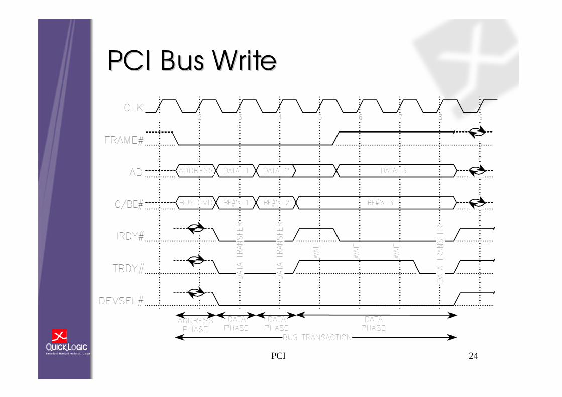
PCI BusPCI Bus WriteWrite

PCI 25
Premature TerminationPremature Termination
z Master Abort– No DEVSEL from any target
z Disconnect– Target can’t continue burst, stop after current
transfer
z Retry– Target can’t complete current cycle, retry later
z Abort– Target has fatal error, don’t retry

PCI 26
Address
42 31 5 6 7 8CLK 9
Bus Cmd
FRAME#
AD
C/BE#
IRDY#
TRDY#
DEVSEL#
Fast
Medium
Slow
Bridge
Master Abort

PCI 27
Disconnect
Data
wai
t
42 31 5 6 7CLK
FRAME#
AD
IRDY#
TRDY#
DEVSEL#
Data
Dat
a tr
ansf
erSTOP#
Dat
a tr
ansf
er
TRDY - True, Stop - True, Devsel - True
PCI 28
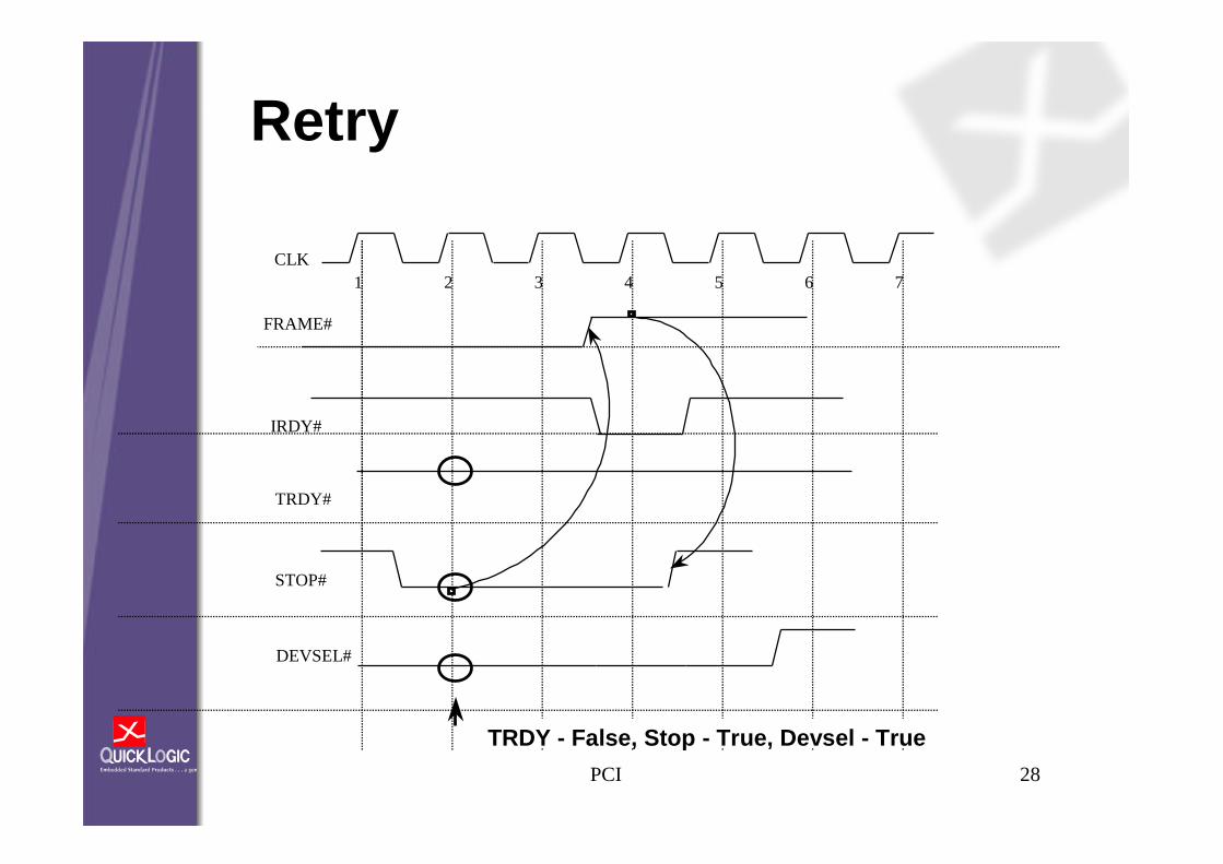
Retry
42 31 5 6 7CLK
FRAME#
IRDY#
TRDY#
DEVSEL#
STOP#
TRDY - False, Stop - True, Devsel - True

PCI 29
Target Abort
42 31 5 6 7CLK
FRAME#
IRDY#
TRDY#
DEVSEL#
STOP#
TRDY - False, Stop - True, Devsel - False

PCIPCI ArbitrationArbitration
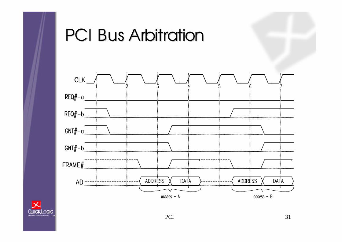
PCI 31
PCI BusPCI Bus ArbitrationArbitration

PCI 32
ArbitrationArbitration
z Arbitration is access based– Master must arbitrate for each bus
access
z Central arbitration scheme– Each master has a unique request
and grant signal
z Arbitration is hidden– Occurs during previous bus cycle

PCI 33
Arbitration SchemeArbitration Scheme
z An arbiter may implement any scheme which is fair– Fairness means that, in general, the
the arbiter must advance to a new agent when the current master releases the bus
– Each potential master must be granted access to the bus independently of other requests
PCI 34
Bus ParkingBus Parking
z Parking permits the arbiter to selectan agent, by asserting its GNT#,when no other agent is using or requesting the bus
z The arbiter determines how this selection is made
• Fixed, Last Used, …, or None

Delayed TransactionsDelayed Transactions
PCI 36
Delayed TransactionsDelayed Transactions
z Used by two types of devices:– I/O Controllers
• Single delayed transaction in general
– Bridges• Particularly PCI-to-PCI bridges• Multiple delayed transactions in
general

PCI 37
ATU
CPU MEM
Local Bus
PCI Bus

PCI 38
Delayed TransactionsDelayed Transactions
z Master issues read
z Slave latches datez Slave terminates with retry
z Slave transfers data from memoryto buffer
z Master issues repeat read
z Slave terminates with TRDY

LatencyLatency
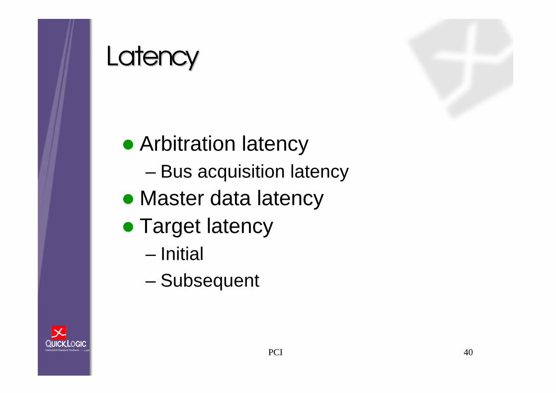
PCI 40
LatencyLatency
z Arbitration latency– Bus acquisition latency
z Master data latencyz Target latency
– Initial– Subsequent

PCI 41
Bus AccessBus Access LatencyLatency
z Number of clocks from the assertionof REQ# to the completion of the first data transaction– Sum of:
• Arbitration Latency• Bus Acquisition Latency• Master Latency• Target Latency

PCI 42
LatencyLatency
Master assertsREQ#
Master receivesGNT#
Master assertsFRAME#
Target assertsTRDY#
ArbitrationLatency
AcquisitionLatency
TargetLatency

PCI 43
LatencyLatency TimerTimer
z Latency Timer (LT) controls trade-offbetween high throughput and low latency
z Latency Timer counter sets minimum number of clocks before the master must surrender GNT#

ExclusiveExclusive AccessAccess
Lock

PCI 45
ExclusiveExclusive AccessAccess
z Lock is an exclusive access mechanism whichalso permits non-exclusive accesses to proceed
z This is referred to as Resource Lock. Ahardware lock can be held across several accesses without interfering with other, non-exclusive, real-time transfers
z This mechanism locks only the target of theoriginal locked access. Other transfers, toagents other than the locked device, may share the bus
z Exclusive access is provided through the use ofthe LOCK# signal

PCI HardwarePCI Hardware

PCI 47
PCI CardPCI Card ConnectorsConnectors
5V 32-Bit Connector
5V 64-Bit Connector
3.3V 32-Bit Connector
3.3V 64-Bit Connector
Keyway
33 MHz
33/66 MHz
Rear Front

PCI 48
5 V To 3.3 V Migration5 V To 3.3 V Migration PathPath
• 5 Volt Card • 3 Volt Card• Dual-Voltage Card
• Key near backpanel• Key away from• 3 Volt
• System• 5 Volt
• System• backpanel

PCI 49
PCIPCI ComponentComponent Pin OutPin Out

PCI 50
Trace LengthTrace Length
Less than 1.5" Trace Length
PCI 51
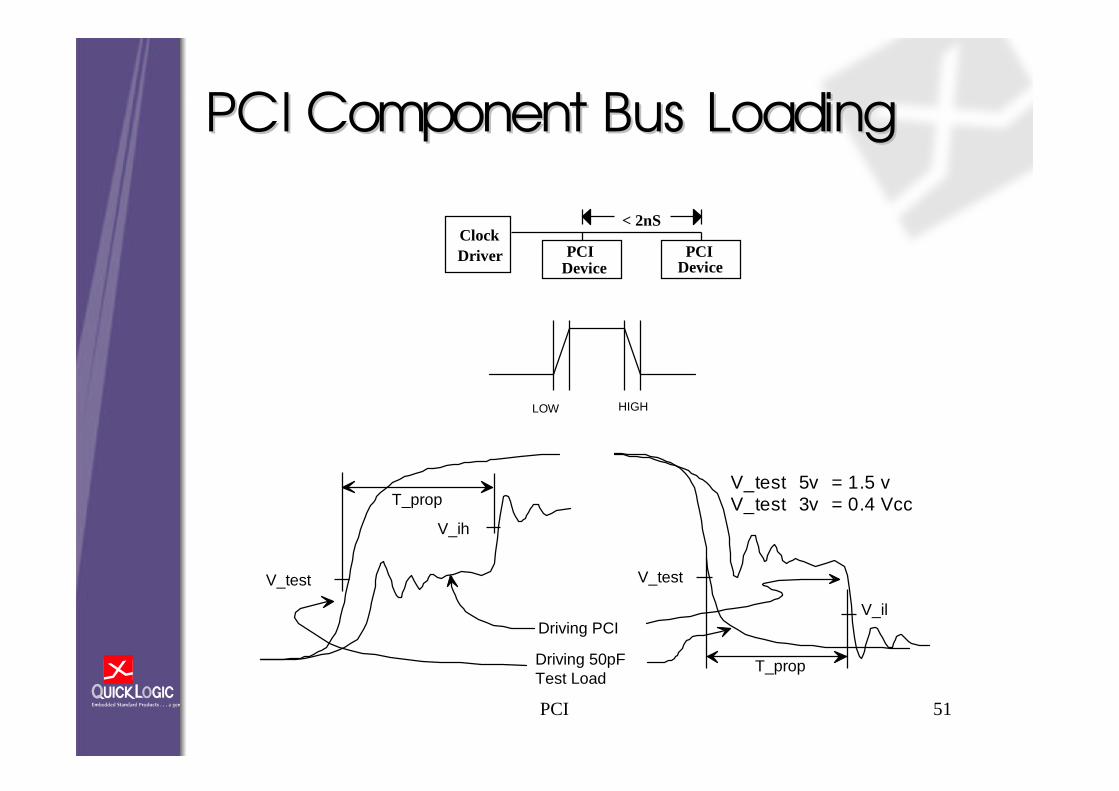
PCIPCI ComponentComponent BusBus LoadingLoading
HIGHLOW
V_ih
V_test
Driving PCI
T_prop
V_il
T_prop
V_test
V_test 5v = 1.5 vV_test 3v = 0.4 Vcc
Driving 50pFTest Load
PCI
< 2nS
DevicePCIDriver
Clock
Device

PCI 52
PCIPCI LoadLoad DefinitionDefinition
z Tprop = 10ns @33MHz, 5ns @ 66MHzz <10 PF per PCI linez <20 NH per PCI linez 60 - 100 Ohms Zz 150 to 190 ps/inch signal velocity (50%C ± 5%)z Shared signals are limited to 1.5 inchesz Unshared signals are limited to 2 inchesz Clock must be 2.5 ± .1 inch, only one loadz Max Clock skew 2ns @ 33MHz, 1ns @ 66 MHzz No maximum number of loads is given in the
specification. Pullup resistor calculations assume10 to be typical, and 16 to be worst case loading

PCI 53
PCIPCI Load RestrictionsLoad Restrictions
It is specifically a violation of the PCI specification to:z Attach an expansion ROM directly, or via bus transceivers, on
any PCI pins– ROM code may not execute in-place
z Attach two or more PCI devices on an expansion board except behind a PCI component
z Attach any logic, other than a single PCI device, which snoopsPCI pins
z Use PCI component sets which place more than one load onany PCI pin,
– Separate address and data path componentsz Use a PCI component which has more than 10pF per pinz Attach any pull-up resistors, or other discrete devices, to PCI
signals except behind PCI component

PCI 54
66MHz Operation66MHz Operation
z PCI operates at 66 MHz only in the 3.3Venvironment
z Agents indicate 66MHz capability both electrically and programmatically– M66EN pin– 66M bit in status register
z Any 33MHz board on the bus grounds the M66EN pin and disables 66 MHzoperation– Pin B49 grounded indicates 33MHz

PCI BIOSPCI BIOS
32-Bit Operating Systems

PCI 56
PCI BIOSPCI BIOS
z Only BIOS is permitted to accessPCI:– Configuration Registers– Interrupt Routing Logic
– Special Cycle generation logic

PCI 57
PCI BIOSPCI BIOS FunctionsFunctions
z Determine configuration mechanismz Detect all PCI buses in the systemz Search for PCI devicesz Read/Write configuration registersz Assign Interrupts to PCI devicesz Determine Special Cycle abilitiesz Permit Special Cycle generation

PCIPCI ConfigurationConfiguration

PCI 59
SystemSystem InitializationInitialization
z Configuration allows software (BIOS) toinitialize the system
z Each device has configuration registers
z At power up software scans bus(es) z Software analyses system
requirements
z Configuration registers are set toconfigure individual devices

PCI 60
Configuration TypesConfiguration Types
z Specific bus commands– configuration read (C/BE# = 1010)– configuration write (C/BE# = 1011)
z Type 0– local PCI bus
• IDSEL line indicates device
• address field indicates register
z Type 1– remote PCI bus (through bridge)
• address field indicates bus, device and register

PCI 61
Configuration Space HeaderConfiguration Space Header
Device ID Vendor ID
CommandStatus
Class Code Rev
Cache Line SizeLatency TimerHeader TypeBIST
Base Address 0
Base Address 1
Base Address 2
Base Address 3
Base Address 4
Base Address 5
Cardbus CIS Pointer
Subsystem Vendor IDSubsystem ID
Expansion ROM Base Address
Reserved
Reserved
Interrupt LineInterrupt PinMin_GntMax_Lat
0004080C1014181C2024282C3034383C

PCI 62
CommandCommand RegisterRegister
Bit Meaning0 I/O Space Enable1 Memory Space Enable2 Bus Master Enable3 Special Cycle Enable4 Memory Write and Invalidate Enable5 VGA Palette Snoop Enable6 Parity Error Enable7 Wait Cycle Control8 SERR# Enable9 Fast Back to Back Enable10:15 Reserved

PCI 63
IDSEL LineIDSEL Line AddressingAddressing
z Addressing the Configuration Space of a device is done using the IDSEL signal as a chip select, and setting AD[1::0] to 00 to indicate a Type 0configuration transaction
z The method used to generate IDSEL is systemspecific, however, if no other mapping is required the following may be used
z The IDSEL of Device 0 is connected to AD[16],Device 1 is connected to AD[17], etc. through Device 16 connected to AD[31]

PCI 64
InterruptInterrupt LineLine
z 8-Bit register which contains interrupt linerouting
z Value in this register is the interrupt number(IRQ) to which the device’s interrupt pin is connected
z If, during initialization, the device requestsan IRQ, one is assigned.
– The IRQ number is placed in this register by configuration software at initialization time

PCI 65
InterruptInterrupt PinPin
z The interrupt pin register indicates which of the four interrupts, INTA#-INTD#, the device or function uses
z A value of 1 corresponds to INTA#, 2 to INTB# etcz Devices which do not use interrupts place 0 in this
registerz This register is read onlyz Each function within a device may use one
interrupt– A single function device must use INTA#– If a multifunction device requires two interrupts
they must be INTA# and INTB# etc.z Interrupts may be shared (chained)
PCI 66
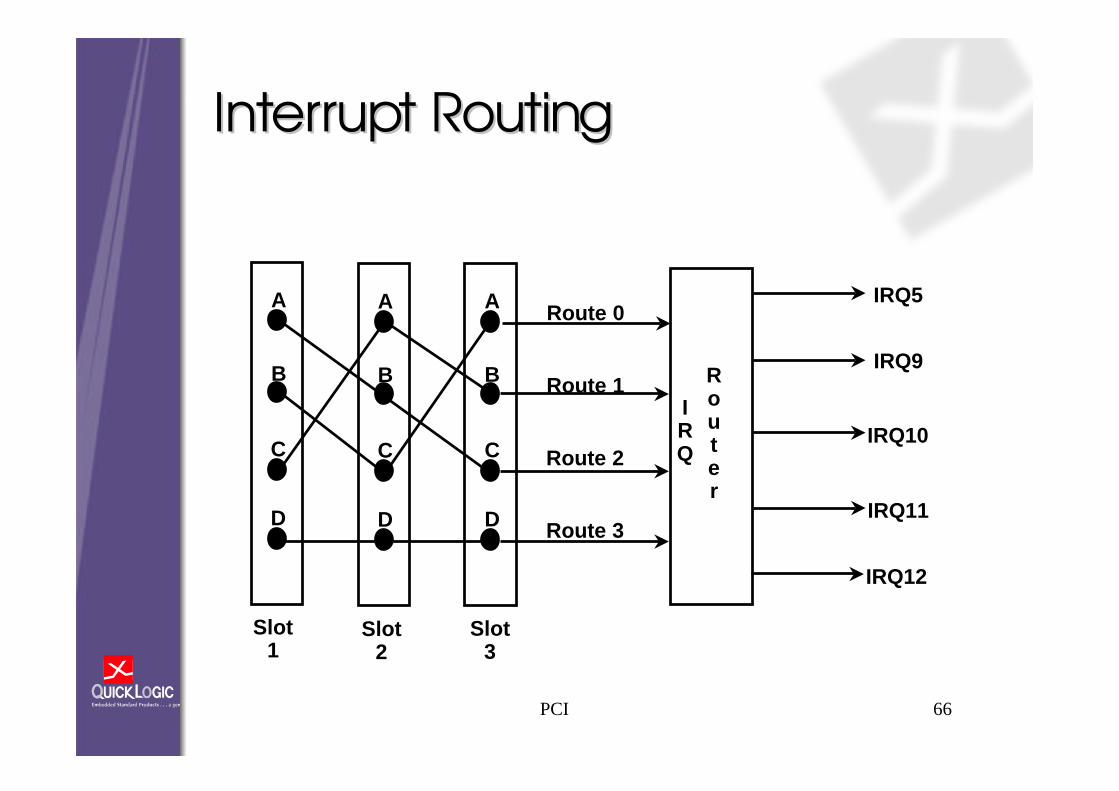
Interrupt RoutingInterrupt Routing
A
B
C
D
A
B
C
D
A
B
C
D
Route 0
Route 1
Route 2
Route 3
IRQ5
IRQ9
IRQ10
IRQ11
IRQ12
IRQ
Router
Slot1
Slot2
Slot3

PCI 67
PCI BusPCI Bus InterruptsInterrupts
Router

PCI 68
MIN_GNT and MAX_LATMIN_GNT and MAX_LAT
z Minimum Grant and Maximum Latencyz MIN_GNT defines the burst-period length
required by the devicez MAX_LAT specifies how often the device must
gain access to the PCI bus– Maximum time between accesses
z Both registers are read only and have agranularity of 250 nanoseconds
z Values of 0 in these registers indicates no majorlatency requirements for the device

PCI 69
DocumentationDocumentation
z PCI Local bus Specification Rev 2.1– PCI Special Interest Group– http://www.pcisig.com/
z PCI System Architecture, 3rd Edition– Mindshare– ISBN# 0-201-40993-3
z PCI Hardware & Software Architecture and Design– Edward Solari & George Willse