Embed Size (px)
Citation preview

ECE Branch GATE Paper 2007
Page : 1
Q.1 to Q.20 carry one mark each
1. If E denotes expectation, the variance of a random variable X is given by (A) E[ ] [X] (B) E[ ] + [X]
(C) E[ ] (D) E2[X]
2. The following plot shows a function which varies linearly with . The value of the integral
2
1
I ydx= ∫ is
(A) 1.0 (B) 2.5
(C) 4.0 (D) 5.0
3. For |x| << 1, coth (x) can be approximated as
(A) x (B) (C)
(D)
4. is (A) 0.5 (B) 1
(C) 2 (D) not defined
5. Which one of the following function is strictly bounded?
(A) (B) (C) (D)
1 2 3 1
1
2
3
y
t

ECE Branch GATE Paper 2007
Page : 2
6. For the function e-x , the linear approximation around is (A) (3 x)e-2 (B) 1 x
(C) ( ) 23 2 2 1 2 x e−+ − +
(D) e-2
7. An independent voltage source in series with an impedance ZS = RS + jXS delivers a maximum
average power to a load impedance ZL when (A) ZL = RS + jXS
(B) ZL = RS
(C) ZL= jXS
(D) ZL = RS jXS
8. The RC circuit shown in the figure is
(A) a low-pass filter (B) a high-pass filter
(C) a band-pass filter (D) a band-reject filter
9. The electron and hole concentration in an intrinsic semiconductor are ni per cm3 at 300 K. Now, if
acceptor impurities are introduced with a concentration of NA per cm3 (where NA ni), the electron concentration per cm3 at 300 K will be (A) ni (B) ni + NA (C) NA ni
(D)
10. In a p+ n junction diode under reverse bias, the magnitude of electric field is maximum at (A) the edge of the depletion region on the p side (B) the edge of the depletion region on the n side (C) the p+ n junction (D) The centre of the depletion region on the n side
11. The correct full wave rectifier circuit is
C R
C
R
ECE Branch GATE Paper 2007
Page : 3
(A)
(B)
(C) (D)
Input
Output
Input
Output
Input
Output
Input
Output

ECE Branch GATE Paper 2007
Page : 4
12. In a transconductance, amplifier, it is desirable to have (A) a large input resistance and a large output resistance (B) a large input resistance and a small output resistance (C) a small input resistance and a large output resistance (D) a small input resistance and a small output resistance
13. X = 01110 and Y = 11001 are two 5-bit binary numbers represented in two’s complement format.
The sum of X and Y represented in two’s complement format using 6 bits is (A) 100111 (B) 001000
(C) 000111 (D) 101001
14. The Boolean function Y = AB + CD is to be realized using only 2-input NAND gates. The
minimum number of gates required is (A) 2 (B) 3
(C) 4 (D) 5
15. If the closed-loop transfer function of a control system is given as T(s) = , then it is
(A) an unstable system (B) an uncontrollable system
(C) a minimum phase system (D) an non-minimum phase system
16. If the Laplace transform of a signal y(t) is Y(s) = ’ then its final value is
(A) 1 (B) 0
(C) 1 (D) Unbounded
17. If R( ) is the autocorrelation function of a real, wide-sense stationary random process, then which
of the following is NOT true? (A) R( ) = R( ) (B) |R( )| R(0) (C) R( ) = R( ) (D) The mean square value of the process is R(0)
18. If S(f) is the power spectral density of a real, wide-sense stationary random process, then which
of the following is ALWAYS true? (A) S(0) S( ) (B) S( ) 0 (C) S ) = S( ) (D)

ECE Branch GATE Paper 2007
Page : 5
19. A plane wave of wavelength λ is travelling in a direction making an angle 30° with positive x-axis and 90° with positive y-axis. The field of the plane wave can be represented as (Ε0 is a constant)
(A)
(B)
(C)
(D)
20. If C is a closed curve enclosing a surface S, then the magnetic field intensity , the current
destiny and the electric flux destiny are related by
(A)
(B)
(C)
(D) Question 21 to Question 75 carry two marks each.
21. It is given that X1, X2 ,…….. XM are M non-zero, orthogonal vectors. The dimension of the vector space spanned by the 2M vector X1, X2, …….. XM, - X1, -X2, …….. XM is (A) 2 M (B) M + 1 (C) M (D) dependent on the choice of X1, X2, …….. XM
22. Consider the function. (x) = - x – 2 .The maximum value of (x) in the closed interval [-4,4] is (A) 18 (B) 10
(C) 2.25 (D) Indeterminate
23. An examination consists of two papers, Paper 1 and Paper 2. The probability of failing in Paper 1
is 0.3 and that in Paper 2 is 0.2. Given that a student has failed in Paper 2, the probability of failing in paper 1 is 0.6. The probability of a student failing in both the papers is (A) 0.5 (B) 0.18
(C) 0.12 (D) 0.06
24. The solution of the differential equation 2
222
d yk y ydx
= − under the boundary conditions (i) y =
y1 at x = 0 and (ii) y2 at x=∞, where k, y1 and y2 are constants, is (A) y = ( ) exp ( x/ ) + (B) y = ( ) exp ( x/ ) +
(C) y = ( ) sin h(x/ ) + (D) y =( ) exp ( x/ ) +

ECE Branch GATE Paper 2007
Page : 6
25. The equation x3 x2 is to be solved using the Newton-Raphson method. If x=2 is taken as the initial approximation of the solution, then the next approximation using this method will be (A)
(B) (C) 1 (D)
26. Three functions , and , which are zero outside the interval [O,T] are shown in the figure. Which of the following statements is correct?
(A) and are orthogonal (B) and are orthogonal
(C) and are orthogonal (D) and are orthonormal
27. If the semi-circular contour D of radius 2 is as shown in the figure, then the value of the integral
is
2 σ 0
D
jω
0
2
2 2 1
1
1
3
T/3
2T/3
t
t
t
T

ECE Branch GATE Paper 2007
Page : 7
(A) j (B) –j
(C) – (D)
28. Two series resonant filters are as shown in the figure. Let the 3-dB bandwidth of Filter 1 to and that of Filter 2 be . The Value of is
(A) 4 (B) 1 (C)
(D)
29. For the circuit shown in the figure, the Thevenin voltage and resistance looking into X –Y are
(A) 4/3 V, 2Ω (B) 4V, 2/3 Ω
(C) 4/3 V, 2/3Ω (D) 4V, 2Ω
30. In the circuit shown, is 0 volts at t = 0, sec. For t > 0, the capacitor current iC (t), where t is in seconds, is given by
2Ω
2A
i
2i
1Ω
1Ω
X
Y
+
R
+
+
-
R
= /4
=4
+
-
+
Filter 1 Filter 2
10V +
-
4 F
20kΩ
20kΩ + -

ECE Branch GATE Paper 2007
Page : 8
(A) 0.50 exp ( 25t)mA (B) 0.25 exp ( 25t)mA
(C) 0.50 exp ( 12.5 t)mA (D) 0.25 exp ( 6.25 t)mA
31. In the AC network shown in the figure, the phasor voltage VAB (in Volts) is
(A) 0 (B) 5∠
(C) 12.5∠ (D) 17∠
32. A p+ n junction has built-in potential of 0.8 V. The depletion layer width at a reverse bias of 1.2 V
is 2 µm. For a reverse bias of 7.2 V, the depletion layer width will be (A) 4 µm (B) 4.9 µm
(C) 8 µm (D) 12 µm
33. Group I lists four types of p-n junction diodes. Match each device in Group I with one of the
Options in Group II to indicate the bias condition of that device in its normal mode of operation Group I Group II P. Zener Diode 1. Forward Bias Q. Solar Cell 2. Reverse Bias R. Laser Diode S. Avalanche Photodiode
(A) P-1, Q-2, R-1, S-2 (B) P-2, Q-1, R-1, S-2
(C) P-2, Q-2, R-1, S-1 (D) P-2, Q-1, R-2, S-2
34. The DC current gain ( ) of a BJT is 50. Assuming that the emitter injection efficiency is 0.995,
the base transport factor is (A) 0.980 (B) 0.985
(C) 0.990 (D) 0.995
-j3Ω
5Ω
5∠30°A
5Ω
j3Ω
A
B
ECE Branch GATE Paper 2007
Page : 9
35. Group I lists four different semiconductor device. Match each device in Group I with its characteristic property in Group II.
Group I Group II P. BJT 1.Population inversion Q. MOS Capacitor 2. Pinch-off Voltage R. Laser Capacitor 3. Early effect S. JFET 4. Flat-band voltage
(A) P-3, Q-1, R-4, S-2 (B) P-2, Q-4, R-3, S-2
(C) P-3, Q-4, R-1, S-2 (D) P-3, Q-2, R-1, S-4
36. For the Op-Amp circuit shown in the figure, is
(A) 2 V (B) 1 V
(C) 0.5 V (D) 0.5 V
37. For the BJT circuit shown, assume that the of the transistor is very large and = 0.7 V. The
mode of operation of the BJT is
10 KΩ
1 KΩ
2 V
1 V
1 KΩ
1 KΩ
2 KΩ
1 KΩ

ECE Branch GATE Paper 2007
Page : 10
(A) cut-off (B) saturation
(C) normal active (D) reverse active
38. In the Op-Amp circuit shown, assume that the diode current follows the equation I = exp
(V/ ). For = 2 V, = , and for = 4 V, = . The relationship between and is
(A) = (B) =
(C) = In 2 (D) = = In 2
39. In the CMOS inverter circuit shown, if the transconductance parameters of the NMOS and PMOS
transistor are = = = = 40 and their threshold voltages are
= = 1 V, the current I is
(A) 0 A (B) 25 (C) 45 (D) 90
2.5 V
NM
PM
5V
I
2 KΩ

ECE Branch GATE Paper 2007
Page : 11
40. For the Zener diode shown in the figure, the Zener voltage at knee is 7 V, the knee current is negligible and the Zener dynamic resistance is 10 . If the input voltage ( ) range is from 10 to 16 V, the output voltage ( ) range from
(A) 7.00 to 7.29 V (B) 7.14 to 7.29 V
(C) 7.14 to 7.43 V (D) 7.29 to 7.43 V
41. The Boolean expression Y = D + + A D + A B can be minimized to
(A) Y = D + + A (B) Y = D + B C + A
(C) Y = + D + A (D) Y = D + A B
42. The circuit diagram of a standard TTL NOT gate is shown in the figure. When = 2.5 V, the
modes of operation of the transistor will be
1.4 k Ω
1 k Ω
= 5 V
4 k Ω 100 k Ω
D
200 Ω
7 V

ECE Branch GATE Paper 2007
Page : 12
(A) : reverse active; : normal active; : saturation; : cut-off (B) : reverse active; : saturation; : saturation; : cut-off (C) : normal active; : cut-off; :cut-off; : saturation (D) : saturation; : saturation; : saturation; : normal active
43. In the following circuit, X is given by
(A) X= A + + + A B C (B) X = B C + A C + A B + (C) X = A B + B C + A C (D) X = +
44. The following binary values were applied to the X and Y inputs of the NAND latch shown in the figure in the sequence indicated below : X = 0, Y = 1, X = 0; Y = 0; X = 1, Y = 1 The corresponding stable P, Q outputs will be
(A) P = 1, Q = 0; P = 1 , Q = 0
P = 1, Q = 0 or P = 0, Q = 1 (B) P = 1, Q = 0; P = 0, Q = 1 or P = 0, Q = 1;
P = 0, Q = 1
(C) P = 1, Q = 0; P = 1, Q = 1; P = 1, Q = 0 or P = 0, Q = 1
(D) P = 1, Q = 0; P = 1, Q = 1; P = 1, Q = 1
45. For the circuit shown, the counter state ( ) follows the sequence
P
Q
X
Y
0 1 1 0
4-to-1 MUX Y
0 1 1 0
4-to-1 MUX Y
A B C
X

ECE Branch GATE Paper 2007
Page : 13
(A) 00, 01, 10, 11, 00….. (B) 00, 01, 10, 00, 01….
(C) 00, 01, 11, 00, 01…. (D) 00, 10, 11, 00, 10…..
46. An 8255 chip is interfaced to an 8085 microprocessor system as an I/O mapped I/O as shown in
the figure. The address lines and of the 8085 are used by the 8255 chip to decode internally its three ports and the Control register. The address lines to as well as the IO signal are used for address decoding. The range of addresses for which the 8255 chip would get selected is
(A) F8H – FBH (B) F8H – FCH
(C) F8H – FFH (D) F0H – F7H
47. The 3-dB bandwidth of the low-pass signal u(t), where u(t) is the unit step function, is given
by (A) Hz
(B)
(C) (D) 1Hz
48. A Hilbert transformer is a
(A) non-linear system (B) non-causal system
(C) time-varying system (D) low-pass system
IO/
8255
Clock

ECE Branch GATE Paper 2007
Page : 14
49. The frequency response of a linear, time-invariant system is given by H( ) = . The step response of the system is (A) 5 (1 )u(t) (B) 5 (1 )u(t) (C) (1 )u(t)
(D) (1 )u(t)
50. A 5 point sequence x[n] is given as x[ 3] = 1, x[ 2] = 1, x[ 1] = 0, x[0] = 5, x[1] = 1. Let X( ) denote the discrete-time Fourier transform of . The value of is (A) 5 (B) 10 (C) 16 (D) 5 + j10
51. The z-transform X[z] of a sequence x[n] is given by X[z] = . It is given that the region of convergence of X[z] includes the unit circle. The value of x[0] is (A) 0.5 (B) 0
(C) 0.25 (D) 0.5
52. A control system with a PD controller is shown in the figure. If the velocity error constant =
1000 and the damping ratio = 0.5, then the values of and are
(A) = 100, = 0.09 (B) = 100, = 0.9
(C) = 10, = 0.09 (D) = 10, = 0.9
53. The transfer function of a plant is T(s) = . The second-order approximation of T(s) using dominant pole concept is (A)
(B)
(C)
(D)
+
y r

ECE Branch GATE Paper 2007
Page : 15
54. The open-loop transfer function of a plant is given as G(s) = . If the plant is operated in a unity feedback configuration, then the lead compensator that can stabilize this control system is (A)
(B)
(C)
(D)
55. A unity feedback control system has an open-loop transfer function G(s) = . The gain K for which s = 1 + j1 will lie on the root locus of this system is (A) 4 (B) 5.5
(C) 6.5 (D) 10
56. The asymptotic Bode plot of a transfer function is as shown in the figure. The transfer function
G(s) corresponding to this Bode plot is
(A)
(B)
(C)
(D)
|G( |(dB)
60
40
20
0
0.1 1 10 100
60 dB/decade
40 dB/decade
20 dB/decade
20

ECE Branch GATE Paper 2007
Page : 16
57. The state space representation of a separately excited DC servo motor dynamics is given as
where is the speed of the motor, is the armature current
and u is the armature voltage. The transfer function of the motor is
(A)
(B)
(C)
(D)
58. In delta modulation, the slope overload distortion can be reduced by (A) decreasing the step size (B) decreasing the granular noise
(C) decreasing the sampling rate (D) increasing the step size
59. The raised cosine pulse p(t) is used for zero ISI in digital communications. The expression for
p(t) with unity roll – off factor is given by p(t) = . The value of p(t) at t = is (A) – 0.5 (B) 0 (C) 0.5 (D)
60. In the following scheme, if the spectrum M( ) of m(t) is as shown, then the spectrum Y( ) of y(t) will be
f 0 + B B
M(f)
cos (2 Bt)
sin (2 Bt)
Hilbert transformer
y(t) +
+
m(t)

ECE Branch GATE Paper 2007
Page : 17
(A)
(B)
(C)
(D)
61. During transmission over a certain binary communication channel, bit errors occur independently with probability p. The probability of AT MOST one bit in error in a block of n bits is given by (A) (B) 1 - (C) np – + – (D) 1 –
f 0 + B B
Y(f)
2B +2B
f 0 + B B
Y(f)
B
Y(f)
+B +2B 2B
0 f
Y(f)
B +B 0 f

ECE Branch GATE Paper 2007
Page : 18
62. In a GSM system, 8 channels can co- exist in 200 kHz bandwidth using TDMA. A GSM based cellular operator is allocated 5 MHz bandwidth. Assuming a frequency reuse factor of , i.e. a five-cell repeat pattern, the maximum number of simultaneous channels that can exist in one cell is (A) 200 (B) 40
(C) 25 (D) 5
63. In a Direct sequence CDMA system the chip rate is chips per second. If the
processing gain is desired to be AT LEAST 100, the data rate (A) must be less than or equal to bits per sec (B) must be greater than bits per sec (C) must be exactly equal to bits per sec (D) can take any value less than bits per sec
64. An air filled rectangular waveguide has inner dimensions of 3cm 2cm. The wave impedance of the mode of propagation in the waveguide at a frequency of 30 GHz is (free space impedance
) (A) 308 (B)
(C) (D)
65. The field (in A/m) of a plane wave propagating in free space is given by
The time average power flow density in watts is (A)
(B)
(C) (D)
66. The field in a rectangular waveguide of inner dimensions is given by
where H0 is a constant, and a and b are the dimensions along the x-axis and the y-axis respectively. The mode of propagation in the waveguide is (A) TE20 (B) TM11
(C) TM20 (D) TE10
67. A load of 50Ω is connected in shunt in a 2-wire transmission line of Z0 =50Ω as shown in the
figure. The 2-port scattering parameter matrix (S-matrix) of the shunt element is

ECE Branch GATE Paper 2007
Page : 19
(A)
(B)
(C)
(D)
68. The parallel branches of a 2-wire transmission line are terminated in 100Ω and 200Ω resistors as
shown in the figure. The characteristic impedance of the line is Z0=50Ω and each section has a length of . The voltage reflection coefficient at the input is
(A)
(B)
(C)
(D)
69. A dipole is kept horizontally at a height of above a perfectly conducting infinite ground plane. The radiation pattern in the plane of the dipole ( plane) looks approximately as
50Ω Z0= 50Ω Z0= 50Ω
Z0 = 50Ω
200Ω
100Ω
=50 Ω
=50 Ω

ECE Branch GATE Paper 2007
Page : 20
70. A right circularly polarized (RCP) plane wave is incident at an angle of 600 to the normal. On an air-dielectric interface. If the reflected wave is linearly polarized, the relative dielectric constant εr2 is
(A) (B)
(C) 2 (D) 3
COMMON DATA QUESTIONS Common Data for Questions 71, 72, 73: The figure shows the high-frequency capacitance- voltage (C-V) characteristics of a Metal/Si /silicon (MOS) capacitor having an area of 1 . Assume that the permittivities ( ) of silicon and Si are 1 F/cm and 3.5 F/cm respectively.
dielectric
600 600
RCP linearly polarized
air
y
y
z
z
z
z
y
y (C)
(A) (B)
(D)

ECE Branch GATE Paper 2007
Page : 21
71. The gate oxide thickness in the MOS capacitor is
(A) 50 nm (B) 143 nm (C) 350 nm (D) 1
72. The maximum depletion layer width in silicon is (A) 0.143 (B) 0.857
(C) 1 (D) 1.143
73. Consider the following statements about the C-V characteristics plot:
S1: The MOS capacitor has an n-type substrate. S2: If positive charge are introduced in the oxide, the C-V plot will shift to the left. Then which of the following is true?
(A) Both S1 and S2 are true (B) S1 is true and S2 is false
(C) S1 is false and S2 is true (D) Both S1 and S2 are false
Common Data for Questions 74, 75: Two 4-ary signal constellations are shown. It is given that constitute an orthonormal basis for the two constellations. Assume that the four symbols in both the constellations are equiprobable. Let denote the power spectral density of white Gaussian noise.
C
V
7 pF
1 pF
0

ECE Branch GATE Paper 2007
Page : 22
74. The ratio of the average energy of constellation 1 to the average of constellation 2 is
(A) 4a2 (B) 4
(C) 2 (D) 8
75. If these constellations are used for digital communications over an AWGN channel, then which
of the following statements is true? (A) Probability of symbol error for Constellation 1 is lower (B) Probability of symbol error for Constellation 1 is higher (C) Probability of symbol error is equal for both the constellations (D) The value of N0 will determine which of the two constellations has a lower probability of
symbol error
Statement for Linked Answer Questions 76 and 77 Consider the Op-Amp circuit shown in the figure.
76. The transfer function (s) (s) is
(A)
(B)
(C)
(D)
R1
C
R
R1
a
a
a
constellation 1
a
a
constellation 2
0 0
a
a 2 a

ECE Branch GATE Paper 2007
Page : 23
77. If and , then the minimum and maximum values of (in radians) are respectively (A) –π/2 and π/2 (B) 0 and π/2
(C) -π and 0 (D) -π/2 and 0
Statement for Linked Answer Questions 78 and 79 An 8085 assembly language program is given below Line 1: MVIA, B5H 2: MVI B, OEH 3: XRI 69H 4: ADD B 5: ANI 9BH 6: CPI 9FH 7: STA 3010H 8: HLT
78. The contents of the accumulator just after execution of the ADD instruction in line 4 will be (A) C3H (B) EAH
(C) DCH (D) 69H
79. After execution of line 7 of the program, the status of the CY and Z flags will be
(A) CY = 0, Z = 0 (B) CY = 0, Z = 1
(C) CY = 1, Z = 0 (D) CY = 1, Z = 1
Statement for Linked Answer Questions 80 and 81 Consider a linear system whose state space representation is (t) = Ax (t). If the initial state
vector of the system is x(0) = , then the system response is x(t) = . If the initial state
vector of the system changes to x (0) = , then the system response becomes x (t) = .
80. The eigenvalue and eigenvector pairs ( for the system are (A) and
(B) and
(C) and
(D) and
81. The system matrix A is
(A)
(B)
(C)
(D)
ECE Branch GATE Paper 2007
Page : 24
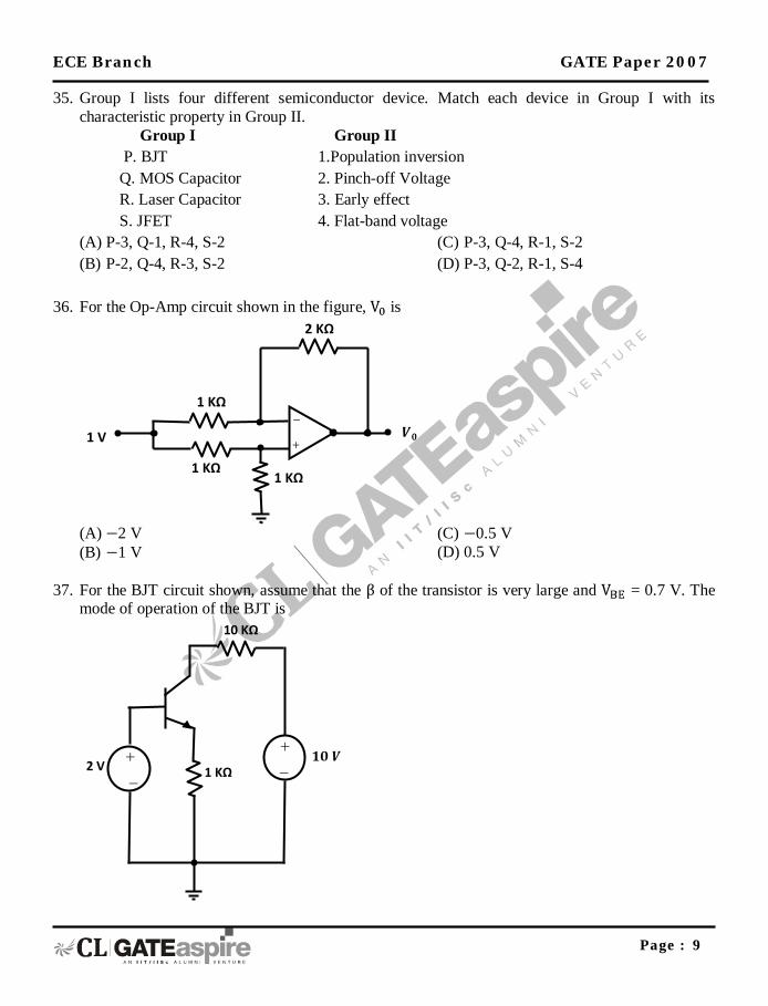
Statement for Linked Answer Questions 82 & 83: An input to a 6-level quantizer has the probability density function f(x) as shown in the figure. Decision boundaries of the quantizer are chosen so as to maximize the entropy of the quantizer output. It is given that 3 consecutive decision boundaries are ‘-1’, ’0’ and ‘1’.
82. The values of a and b are
(A) a = 1/6 and b = 1/12 (B) a = 1/5 and b = 3/40
(C) a = 1/4 and b = 1/16 (D) a = 1/3 and b = 1/24
83. Assuming that the reconstruction levels of the quantizer are the mid-points of the decision
boundaries, the ratio of signal power to quantization noise power is (A)
(B)
(C) (D) 28
Statement for Linked Answer Questions 84 and 85 In the Digital-to-Analog converter circuit shown in the figure below, = 10 V and R = 10 kΩ
84. The current is
(A) 31.25 (B) 62.5
(C) 125 (D) 250
2R
2R 2R 2R
-
R
R R R 2R i
+ 10
f(x)
5 1 0 1 5 x
b
a

ECE Branch GATE Paper 2007
Page : 25
85. The voltage is (A) -0.781 V (B) -1.562 V
(C) -3.125 V (D) -6.250 V


![2’s Complement and Floating-Point - University of …...Two’s Complement •An n-bit, two’s complement number can represent the range [−2!−1, 2 !−1− 1]. • Note the](https://img.pdfslide.us/doc/110x75/5e6c27f608fa3e72a23f5faa/2as-complement-and-floating-point-university-of-twoas-complement-aan.jpg)