Embed Size (px)
Citation preview

Quasi-Resonant Controllers with Integrated Power MOSFET STR-Y6700 Series
STR-Y6700 - DS Rev.4.1 SANKEN ELECTRIC CO.,LTD. 1 Jun. 09, 2016
General Descriptions The STR-Y6700 series are power ICs for switching
power supplies, incorporating a MOSFET and a quasi-resonant controller IC.
Including an auto standby function in the controller, the product achieves the low standby power by the automatic switching between the PWM operation in normal operation, one bottom-skip operation under medium to light load conditions and the burst-oscillation under light load conditions.
The product achieves high cost-performance power supply systems with few external components.
Features • Multi-mode Control
The optimum operation depending on load conditions is changed automatically and is achieved high efficiency operation across the full range of loads. Operation Mode Normal load ------------------------- Quasi-resonant mode Medium to light load ------------- One bottom-skip mode Light load -------------------------- Burst oscillation mode
(Auto standby function) • No load power consumption
PIN < 30 mW (100VAC) PIN < 50 mW (230VAC)
• Leading Edge Blanking Function • Bias Assist Function • Built-in startup circuit reduces • Protections
Overcurrent Protection 1 (OCP1): Pulse-by-Pulse, with Input Compensation Function Overcurrent Protection 2 (OCP2)(1): Latched shutdown Overload Protection (OLP): Latched shutdown Overvoltage Protection (OVP): Latched shutdown Thermal Shutdown Protection (TSD): Latched shutdown (1) Products with the last letter "A" don’t have the OCP2 function.
Typical Application
NF
GN
DFB
/OLP
S/O
CP
VC
C
D/S
T2
1 7542 3
STR-Y6700
6
BD
VAC
C1
D2 R2
C3
T1 D51
C51
R51
R52
U51
R54
R56
C52
D
P
S
PC1
PC1C4ROCP
CY
BR1
R53
R55
L51
C53
C5
RBD2
RBD1
DZBD
CBD
R3
U1
VOUT(+)
VOUT(-)
Package TO220F-7L
Not to Scale Lineup • Electrical Characteristics
Products VDSS(min.) RDS(ON)(max.) STR–Y6735 STR–Y6735A 500 V 0.8 Ω
STR–Y6753 650 V
1.9 Ω STR–Y6754 1.4 Ω STR–Y6766 STR–Y6766A
800 V
1.7 Ω
STR–Y6765 2.2 Ω STR–Y6763 STR–Y6763A 3.5 Ω
• Output Power, POUT
(2)
Products POUT (Open frame)
380VDC 85~265VAC STR–Y6735 STR–Y6735A 120 W(100VAC) –
STR–Y6753 100 W 60 W STR–Y6754 120 W 67 W STR–Y6766 STR–Y6766A 140 W 80 W
STR–Y6765 120 W 70 W STR–Y6763 STR–Y6763A 80 W 50 W
(2) The output power is actual continues power that is measured at 50 °C ambient. The peak output power can be 120 to 140 % of the value stated here. Core size, ON Duty, and thermal design affect the output power. It may be less than the value stated here.
Applications • White goods • Office automation equipment • Industrial equipment
http://www.sanken-ele.co.jp/en/

STR-Y6700 Series
STR-Y6700 - DS Rev.4.1 SANKEN ELECTRIC CO.,LTD. 2 Jun. 09, 2016
CONTENTS General Descriptions ------------------------------------------------------------------------------------------ 1 1. Absolute Maximum Ratings ----------------------------------------------------------------------------- 3 2. Electrical Characteristics -------------------------------------------------------------------------------- 4 3. Performance Curves -------------------------------------------------------------------------------------- 6
3.1 Derating Curves ------------------------------------------------------------------------------------ 6 3.2 Ambient Temperature versus Power Dissipation Curves ---------------------------------- 6 3.3 MOSFET Safe Operating Area Curves ------------------------------------------------------- 8 3.4 Transient Thermal Resistance Curves --------------------------------------------------------- 9
4. Block Diagram ------------------------------------------------------------------------------------------- 10 5. Pin Configuration Definitions ------------------------------------------------------------------------- 10 6. Typical Application ------------------------------------------------------------------------------------- 11 7. Physical Dimensions ------------------------------------------------------------------------------------ 12 8. Marking Diagram --------------------------------------------------------------------------------------- 12 9. Operational Description ------------------------------------------------------------------------------- 13
9.1 Startup Operation ------------------------------------------------------------------------------- 13 9.2 Undervoltage Lockout (UVLO) --------------------------------------------------------------- 13 9.3 Bias Assist Function ----------------------------------------------------------------------------- 13 9.4 Soft Start Function ------------------------------------------------------------------------------ 14 9.5 Constant Output Voltage Control ------------------------------------------------------------ 15 9.6 Leading Edge Blanking Function ------------------------------------------------------------- 15 9.7 Quasi-Resonant Operation and Bottom-On Timing Setup ------------------------------ 15
9.7.1 Quasi-Resonant Operation ------------------------------------------------------------ 15 9.7.2 Bottom-On Timing Setup ------------------------------------------------------------- 16
9.8 BD Pin Blanking Time -------------------------------------------------------------------------- 17 9.9 Multi-mode Control ----------------------------------------------------------------------------- 18
9.9.1 One Bottom-Skip Quasi-Resonant Operation ------------------------------------- 18 9.9.2 Automatic Standby Mode Function ------------------------------------------------- 19
9.10 Maximum On-Time Limitation Function --------------------------------------------------- 19 9.11 Overcurrent Protection (OCP) ---------------------------------------------------------------- 20
9.11.1 Overcurrent Protection 1 (OCP1) --------------------------------------------------- 20 9.11.2 Overcurrent Protection 2 (OCP2) --------------------------------------------------- 20 9.11.3 OCP1 Input Compensation Function ----------------------------------------------- 20 9.11.4 When Overcurrent Input Compensation is Not Required ---------------------- 23
9.12 Overload Protection (OLP) -------------------------------------------------------------------- 23 9.13 Overvoltage Protection (OVP) ---------------------------------------------------------------- 24 9.14 Thermal Shutdown (TSD) ---------------------------------------------------------------------- 24
10. Design Notes ---------------------------------------------------------------------------------------------- 25 10.1 External Components --------------------------------------------------------------------------- 25 10.2 Transformer Design ----------------------------------------------------------------------------- 27 10.3 PCB Trace Layout and Component Placement -------------------------------------------- 28
11. Pattern Layout Example ------------------------------------------------------------------------------- 30 12. Reference Design of Power Supply ------------------------------------------------------------------ 31 IMPORTANT NOTES ------------------------------------------------------------------------------------- 33

STR-Y6700 Series
STR-Y6700 - DS Rev.4.1 SANKEN ELECTRIC CO.,LTD. 3 Jun. 09, 2016
1. Absolute Maximum Ratings • Current polarities are defined as follows: a current flow going into the IC (sinking) is positive current (+); and a
current flow coming out of the IC (sourcing) is negative current (−). • Unless otherwise specified TA = 25 °C
Parameter Symbol Test Conditions Pins Rating Units Notes
Drain Peak Current(1) IDPEAK Single pulse 1 – 2
6.7
A
STR–Y6763 / 63A
8.9 STR–Y6765
9.2 STR–Y6753
10.5 STR–Y6766 / 66A
11.0 STR–Y6754
14.6 STR–Y6735 / 35A
Maximum Switching Current(2) IDMAX Single pulse Ta= −20 to 125°C 1 – 2
6.7
A
STR–Y6763 / 63A
8.9 STR–Y6765
9.2 STR–Y6753
10.5 STR–Y6766 / 66A
11.0 STR–Y6754
14.6 STR–Y6735 / 35A
Avalanche Energy(3)(4) EAS
ILPEAK=2.3A
1 – 2
60
mJ
STR–Y6763 / 63A ILPEAK=2.6A 77 STR–Y6765 ILPEAK=2.9A 99 STR–Y6753 ILPEAK=3.2A 116 STR–Y6766 / 66A ILPEAK=4.1A 198 STR–Y6754 ILPEAK=3.5A 152 STR–Y6735 / 35A
D/ST Pin Voltage VSTARTUP 1 − 4 − 1.0 to VDSS V
S/OCP Pin Voltage VOCP 2 – 4 − 2.0 to 6.0 V
VCC Pin Voltage VCC 3 – 4 35 V
FB/OLP Pin Voltage VFB 5 – 4 − 0.3 to 7.0 V
FB/OLP Pin Sink Current IFB 5 – 4 10.0 mA
BD Pin Voltage VBD 6 – 4 − 6.0 to 6.0 V
Power Dissipation(5) PD1 With infinite heatsink 1 – 2
19.9
W
STR–Y6763 / 63A
21.8 STR–Y6765
20.2 STR–Y6753
23.6 STR–Y6766 / 66A
21.5 STR–Y6735 / 35A STR–Y6754
Without heatsink 1 – 2 1.8 W
Control Part Power Dissipation PD2 VCC×ICC 3 – 4 0.8 W Internal Frame Temperature in Operation TF − − 20 to 115 °C
Operating Ambient Temperature TOP − − 20 to 115 °C Storage Temperature Tstg − − 40 to 125 °C Junction Temperature Tch − 150 °C
(1) Refer to 3.3 MOSFET Safe Operating Area Curves (2) The maximum switching current is the drain current determined by the drive voltage of the IC and threshold voltage
(Vth) of the MOSFET. (3) Refer to Figure 3-2 Avalanche Energy Derating Coefficient Curve (4) Single pulse, VDD = 99 V, L = 20 mH (5) Refer to 3.2 TA-PD1curves.

STR-Y6700 Series
STR-Y6700 - DS Rev.4.1 SANKEN ELECTRIC CO.,LTD. 4 Jun. 09, 2016
2. Electrical Characteristics • The polarity value for current specifies a sink as "+," and a source as "−," referencing the IC. • Unless otherwise specified, TA = 25 °C, VCC = 20 V
Parameter Symbol Test Conditions Pins Min. Typ. Max. Units Notes
Power Supply Startup Operation
Operation Start Voltage VCC(ON) 3 − 4 13.8 15.1 17.3 V
Operation Stop Voltage(1) VCC(OFF) 3 − 4 8.4 9.4 10.7 V
Circuit Current in Operation ICC(ON) 3 − 4 − 1.3 3.7 mA Circuit Current in Non-Operation ICC(OFF) VCC = 13 V 3 − 4 − 4.5 50 µA
Startup Circuit Operation Voltage VSTART(ON) 1 − 4 42 57 72 V
Startup Current ICC(STARTUP) VCC = 13 V 3 − 4 − 4.5 − 3.1 − 1.0 mA Startup Current Biasing Threshold Voltage VCC(BIAS) 3 − 4 9.5 11.0 12.5 V
PWM Switching Frequency fOSC 1 − 4 18.4 21.0 24.4 kHz
Soft Start Operation Duration tSS 1 − 4 − 6.05 − ms
Normal Operation Bottom-Skip Operation Threshold Voltage 1 VOCP(BS1) 2 − 4 0.487 0.572 0.665 V
Bottom-Skip Operation Threshold Voltage 2 VOCP(BS2) 2 − 4 0.200 0.289 0.380 V
Quasi-Resonant Operation Threshold Voltage 1 VBD(TH1) 6 − 4 0.14 0.24 0.34 V
Quasi-Resonant Operation Threshold Voltage 2(2) VBD(TH2) 6 − 4 0.07 0.17 0.27 V
Maximum Feedback Current IFB(MAX) 5 − 4 −320 −205 −120 µA
Standby Operation Standby Operation Threshold Voltage VFB(STBOP) 5 − 4 0.45 0.80 1.15 V
Protected Operation
Maximum On-Time tON(MAX) 1 − 4 30.0 40.0 50.0 µs
Leading Edge Blanking Time tON(LEB) 1 − 4 − 455 −
ns
STR–Y6735 / 35A/ 65/ 66/ 54
− 470 − STR–Y6763 / 63A/ 53
Overcurrent Detection 1 Threshold Voltage in Input Compensation Operation
VOCP(L) VBD = –3V 2 − 4 0.560 0.660 0.760 V
Overcurrent Detection 1 Threshold Voltage in Normal Operation
VOCP(H) VBD = 0V 2 − 4 0.820 0.910 1.000 V
Overcurrent Detection 2 Threshold Voltage VOCP(La.OFF) 2 − 4 1.65 1.83 2.01 V
Products without the last letter "A"
(1) VCC(OFF) < VCC(BIAS) always. (2) VBD(TH2) < VBD(TH1) always.

STR-Y6700 Series
STR-Y6700 - DS Rev.4.1 SANKEN ELECTRIC CO.,LTD. 5 Jun. 09, 2016
Parameter Symbol Test Conditions Pins Min. Typ. Max. Units Notes
BD Pin Source Current IBD(O) 6 − 4 − 250 − 83 − 30 µA
OLP Bias Current IFB(OLP) 5 − 4 − 15 − 10 − 5 µA
OLP Threshold Voltage VFB(OLP) 5 − 4 5.50 5.96 6.40 V
FB Pin Maximum Voltage in Feedback Operation VFB(MAX) 5 − 4 3.70 4.05 4.40 V
OVP Threshold Voltage VCC(OVP) 3− 4 28.5 31.5 34.0 V
Thermal Shutdown Operating Temperature Tj(TSD) − 135 − − °C
MOSFET
Drain-to-Source Breakdown Voltage VDSS IDS=300μA 1 – 2
500 − −
V
STR-Y6735 / 35A
650 − − STR-Y6753 / 54
800 − − STR-Y6763 / 63A / 65 /66 /66A
Drain Leakage Current IDSS VDS=VDSS 1 – 2 − − 300 μA
On Resistance RDS(ON) 1 – 2
− − 0.8
Ω
STR-Y6735 / 35A
− − 1.4 STR–Y6754
1.7 STR–Y6766 / 66A
1.9 STR–Y6753
2.2 STR–Y6765
− − 3.5 STR–Y6763 / 63A
Switching Time tf 1 – 2 − − 250 ns STR–Y6753
/ 63 / 63A
− − 300 ns STR-Y6735 / 35A / 54 / 66 / 66A / 65
Thermal Resistance
Channel to Frame Thermal Resistance(3) θch-F
−
− 2.4 2.7
°C/W
STR-Y6735 / 35A / 54
− 1.9 2.2 STR–Y6766 / 66A
− 2.7 3.1 STR–Y6753
− 2.3 2.6 STR–Y6765
− 2.8 3.2 STR–Y6763 / 63A
Channel to Case Thermal Resistance(4) θch-C
−
− 5.1 5.9
°C/W
STR-Y6735 / 35A / 54
− 4.6 5.3 STR–Y6766 / 66A
− 5.4 6.2 STR–Y6753
− 5.0 5.8 STR–Y6765
− 5.5 6.3 STR–Y6763 / 63A
(3) θch-F is thermal resistance between channel and internal frame. (4) θch-C is thermal resistance between channel and case. Case temperature is measured at the backside surface.

STR-Y6700 Series
STR-Y6700 - DS Rev.4.1 SANKEN ELECTRIC CO.,LTD. 6 Jun. 09, 2016
3. Performance Curves
3.1 Derating Curves
Figure 3-1 SOA Temperature Derating Coefficient Curve Figure 3-2 Avalanche Energy Derating Coefficient Curve
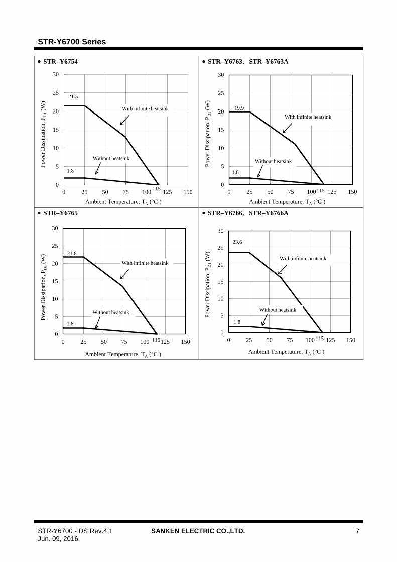
3.2 Ambient Temperature versus Power Dissipation Curves
• STR–Y6735、STR–Y6735A • STR–Y6753
0
20
40
60
80
100
0 25 50 75 100 125
Safe
Ope
ratin
g A
rea
Tem
pera
ture
Der
atin
g C
oeffi
cien
t (%
)
Internal frame temperature, TF (°C)
0
20
40
60
80
100
25 50 75 100 125 150E AS
Tem
pera
ture
Der
atin
g C
oeffi
cien
t (%
)
Channel Temperature, Tch (°C)
0
5
10
15
20
25
30
0 25 50 75 100 125 150
Pow
er D
issi
patio
n, P
D1
(W)
Ambient Temperature, TA (°C )
1.8
21.5
115
With infinite heatsink
Without heatsink
0
5
10
15
20
25
30
0 25 50 75 100 125 150
Pow
er D
issi
patio
n, P
D1
(W)
Ambient Temperature, TA (°C )
1.8
20.2
115
With infinite heatsink
Without heatsink
115
STR-Y6700 Series
STR-Y6700 - DS Rev.4.1 SANKEN ELECTRIC CO.,LTD. 7 Jun. 09, 2016
• STR–Y6754 • STR–Y6763、STR–Y6763A
• STR–Y6765 • STR–Y6766、STR–Y6766A
0
5
10
15
20
25
30
0 25 50 75 100 125 150
Pow
er D
issi
patio
n, P
D1
(W)
Ambient Temperature, TA (°C )
With infinite heatsink
Without heatsink
1.8
21.5
1150
5
10
15
20
25
30
0 25 50 75 100 125 150
Pow
er D
issi
patio
n, P
D1
(W)
Ambient Temperature, TA (°C )
1.8
19.9
115
With infinite heatsink
Without heatsink
0
5
10
15
20
25
30
0 25 50 75 100 125 150
Pow
er D
issi
patio
n, P
D1
(W)
Ambient Temperature, TA (°C )
1.8
21.8
115
With infinite heatsink
Without heatsink
0
5
10
15
20
25
30
0 25 50 75 100 125 150
Pow
er D
issi
patio
n, P
D1
(W)
Ambient Temperature, TA (°C )
1.8
23.6
115
With infinite heatsink
Without heatsink

STR-Y6700 Series
STR-Y6700 - DS Rev.4.1 SANKEN ELECTRIC CO.,LTD. 8 Jun. 09, 2016
3.3 MOSFET Safe Operating Area Curves • When the IC is used, the safe operating area curve should be multiplied by the temperature derating coefficient
derived from Figure 3-1. • The broken line in the safe operating area curve is the drain current curve limited by on-resistance. • Unless otherwise specified, TA = 25 °C, Single pulse
• STR–Y6735, STR–Y6735A • STR–Y6753
• STR–Y6754 • STR–Y6763, STR–Y6763A
• STR–Y6765 • STR–Y6766, STR–Y6766A
0.1
1
10
100
10 100 1000
Dra
in C
urre
nt, I
D(A
)
Drain-to-Source Voltage (V)
0.01
0.1
1
10
100
10 100 1000
Dra
in C
urre
nt, I
D(A
)
Drain-to-Source Voltage (V)
0.1
1
10
100
10 100 1000
Dra
in C
urre
nt, I
D(A
)
Drain-to-Source Voltage (V)
0.01
0.1
1
10
10 100 1000
Dra
in C
urre
nt, I
D(A
)
Drain-to-Source Voltage (V)
0.01
0.1
1
10
10 100 1000
Dra
in C
urre
nt, I
D(A
)
Drain-to-Source Voltage (V)
0.1
1
10
100
10 100 1000
Dra
in C
urre
nt, I
D(A
)
Drain-to-Source Voltage (V)
0.1ms
1ms
0.1ms
1ms
0.1ms
1ms
0.1ms
1ms
0.1ms
1ms
0.1ms
1ms

STR-Y6700 Series
STR-Y6700 - DS Rev.4.1 SANKEN ELECTRIC CO.,LTD. 9 Jun. 09, 2016
3.4 Transient Thermal Resistance Curves
• STR–Y6735, STR–Y6735A, STR–Y6754, STR–Y6765
• STR–Y6753, STR–Y6763, STR–Y6763A
• STR–Y6766, STR–Y6766A
0.001
0.01
0.1
1
10
Tran
sien
t The
rmal
Res
ista
nce
θch-
c (°
C/W
)
Time (s)
0.001
0.01
0.1
1
10
Tran
sien
t The
rmal
Res
ista
nce
θch-
c (°
C/W
)
Time (s)
0.001
0.01
0.1
1
10
Tran
sien
t The
rmal
Res
ista
nce
θch-
c (°
C/W
)
Time (s)
1µ 10µ 100µ 1m 10m 100m
1µ 10µ 100µ 1m 10m 100m
1µ 10µ 100µ 1m 10m 100m

STR-Y6700 Series
STR-Y6700 - DS Rev.4.1 SANKEN ELECTRIC CO.,LTD. 10 Jun. 09, 2016
4. Block Diagram
UVLOReg / ICONST
STARTUPVCC
GND
D/ST
S/OCP
BD
1
2
64
3
BD_STR-Y6700_R1
FB/OLP5
NF7
LATCHLOGIC
OSC
BD
FB/STBOLP
OCP/BS
DRV
5. Pin Configuration Definitions
1
5
D/ST
S/OCPVCCGNDFB/OLPBD
(LF3051)
2
4
6
7 NF
3
Pin Name Descriptions
1 D/ST MOSFET drain and startup current input
2 S/OCP MOSFET source and overcurrent protection (OCP) signal input
3 VCC Power supply voltage input for control part and overvoltage protection (OVP) signal input
4 GND Ground
5 FB/OLP Constant voltage control signal input and over load protection (OLP) signal input
6 BD Bottom Detection signal input, Input Compensation detection signal input
7 NF* (Non-function)
*For stable operation, NF pin should be connected to GND pin, using the shortest possible path.

STR-Y6700 Series
STR-Y6700 - DS Rev.4.1 SANKEN ELECTRIC CO.,LTD. 11 Jun. 09, 2016
6. Typical Application • The PCB traces D/ST pins should be as wide as possible, in order to enhance thermal dissipation. • In applications having a power supply specified such that D/ST pin has large transient surge voltages, a clamp
snubber circuit of a capacitor-resistor-diode (CRD) combination should be added on the primary winding P, or a damper snubber circuit of a capacitor (C) or a resistor-capacitor (RC) combination should be added between the D/ST pin and the S/OCP pin.
• For stable operation, NF pin should be connected to GND pin, using the shortest possible path.
NF
GN
DFB
/OLP
S/O
CP
VC
C
D/S
T2
1 7542 3
STR-Y6700
6
BD
VAC
C1
D2 R2
C3
T1 D51
C51
R51
R52
U51
R54
R56
C52
D
P
S
PC1
PC1C4ROCP
CY
BR1
R53
R55
L51
C53
CV
C5
RBD2
RBD1
DZBD
CBD
R3
U1
VOUT(+)
VOUT(-)
C2 R1
D1
CRD clamp snubber
C(RC)Damper snubber
Figure 6-1 Typical application

STR-Y6700 Series
STR-Y6700 - DS Rev.4.1 SANKEN ELECTRIC CO.,LTD. 12 Jun. 09, 2016
7. Physical Dimensions • TO220F-7L
0.5 0.50.5 0.5
0.45+0.2-0.1
R-endR-end
2.6±0.1
2.6
4.2
3.2
+0.2
2.8
±0.152
10.4±
0.5
15
10
1 2 3 4 5 6 7
±0.2
(1.1)
±0.2
±0.2
5×P1.17±0.15=5.85±0.15
±0.3
±0.2
(5.6)
Gate burr
(Measured at pin base)(Measured at pin base) (Measured at pin tip)
2.54±0.6
(Measured at pin tip)5.08±0.6
5±0.5
5±0.5
±0.157-0.62
-0.1+0.27-0.55
(Measured at pin base)
Front view Side view
NOTES : 1) Dimension is in millimeters. 2) Leadform: LF No.3051 3) Gate burr indicates protrusion of 0.3 mm (max.). 4) Pin treatment Pb-free. Device composition compliant with the RoHS directive.
8. Marking Diagram
2
1 7
Part Number
STRY 6 7 × × ×
Y M D D XLot Number: Y is the last digit of the year of manufacture (0 to 9) M is the month of the year (1 to 9, O, N or D) DD is the day of the month (01 to 31) X is the control number
2

STR-Y6700 Series
STR-Y6700 - DS Rev.4.1 SANKEN ELECTRIC CO.,LTD. 13 Jun. 09, 2016
9. Operational Description • All of the parameter values used in these descriptions
are typical values, unless they are specified as minimum or maximum.
• With regard to current direction, "+" indicates sink current (toward the IC) and "–" indicates source current (from the IC).
9.1 Startup Operation Figure 9-1 shows the circuit around IC. Figure 9-2
shows the start up operation.
VACC1
D2 R2
C3
T1
D
P
BR1
VCC
GND
D/ST1
4
3U1
VD
Figure 9-1 VCC pin peripheral circuit
VCC(ON)
VCC pin voltage
Drain current, ID
tSTART
Figure 9-2 Startup operation
The IC incorporates the startup circuit. The circuit is connected to D/ST pin. When D/ST pin voltage reaches to Startup Circuit Operation Voltage VSTART(ON) = 57 V, the startup circuit starts operation.
During the startup process, the constant current, ICC(STARTUP) = − 3.1 mA, charges C3 at VCC pin. When VCC pin voltage increases to VCC(ON) = 15.1 V, the control circuit starts operation. During the IC operation, the voltage rectified the auxiliary winding voltage, VD, of Figure 9-1 becomes a power source to the VCC pin. After switching operation begins, the startup circuit turns off automatically so that its current consumption becomes zero.
The approximate value of auxiliary winding voltage is about 20 V, taking account of the winding turns of D
winding so that VCC pin voltage becomes Equation (1) within the specification of input and output voltage variation of power supply.
.)(minVV.)(maxV )OVP(CCCC)BIAS(CC <<
⇒12.5 (V) << CCV 28.5 (V) (1)
The startup time of IC is determined by C3 capacitor value. The approximate startup time tSTART (shown in Figure 9-2) is calculated as follows:
)STRATUP(CC
)INT(CC)ON(CCSTART I
VV×C3t
-= (2)
where, tSTART : Startup time of IC (s) VCC(INT) : Initial voltage on VCC pin (V)
9.2 Undervoltage Lockout (UVLO) Figure 9-3 shows the relationship of VCC pin voltage
and circuit current ICC. When VCC pin voltage decreases to VCC(OFF) = 9.4 V, the control circuit stops operation by Undervoltage Lockout (UVLO) circuit, and reverts to the state before startup.
Circuit current, ICC
VCC(OFF) VCC(ON)VCC pin voltage
StartStop
Figure 9-3 Relationship between VCC pin voltage and ICC
9.3 Bias Assist Function By the Bias Assist Function, the startup failure is
prevented and the latched state is kept. The Bias Assist function is activated, when the VCC
voltage decreases to the Startup Current Biasing Threshold Voltage, VCC(BIAS) = 11.0 V, in either of following condition: the FB pin voltage is the Standby Operation Threshold Voltage, VFB(STBOP) = 0.80 V or less or the IC is in the latched state due to activating the protection function.

STR-Y6700 Series
STR-Y6700 - DS Rev.4.1 SANKEN ELECTRIC CO.,LTD. 14 Jun. 09, 2016
When the Bias Assist Function is activated, the VCC pin voltage is kept almost constant voltage, VCC(BIAS) by providing the startup current, ISTARTUP, from the startup circuit. Thus, the VCC pin voltage is kept more than VCC(OFF).
Since the startup failure is prevented by the Bias Assist Function, the value of C3 connected to VCC pin can be small. Thus, the startup time and the response time of the OVP become shorter.
The operation of the Bias Assist Function in startup is
as follows. It is necessary to check and adjust the startup process based on actual operation in the application, so that poor starting conditions may be avoided.
Figure 9-4 shows VCC pin voltage behavior during
the startup period. After VCC pin voltage increases to VCC(ON) = 15.1 V
at startup, the IC starts the operation. Then circuit current increases and VCC pin voltage decreases. At the same time, the auxiliary winding voltage VD increases in proportion to output voltage. These are all balanced to produce VCC pin voltage.
When VCC pin voltage is decrease to VCC(OFF) = 9.4 V in startup operation, the IC stops switching operation and a startup failure occurs.
When the output load is light at startup, the output voltage may become more than the target voltage due to the delay of feedback circuit. In this case, the FB pin voltage is decreased by the feedback control. When the FB pin voltage decreases to the Standby Operation Threshold Voltage, VFB(STBOP) = 0.80 V, or less, the IC stops switching operation and VCC pin voltage decreases. When VCC pin voltage decreases to VCC(BIAS), the Bias Assist function is activated and the startup failure is prevented.
IC starts operation VCC pin voltage
VCC(ON)
VCC(BIAS)
VCC(OFF)
Startup failure
Startup success
Target operating voltage
Time
Bias assist period
Increase with rising of output voltage
Figure 9-4 VCC pin voltage during startup period
9.4 Soft Start Function Figure 9-5 shows the behavior of VCC pin voltage,
drain current and BD pin voltage during the startup period.
The IC activates the soft start circuitry during the startup period. Soft start is fixed to tSS = 6.05 ms. During the soft start period, over current threshold is increased
step-wisely (4 steps). This function reduces the voltage and the current stress of MOSFET and secondary side rectifier diode.
During the soft start operation period, the operation is in PWM operation, at an internally set operation frequency, fOSC = 21.0 kHz.
Until BD pin voltage becomes the following condition after the soft start time, the switching operation is PWM control of fOSC = 21.0 kHz.
When BD pin voltage, VBD, becomes the following condition, the IC starts quasi-resonant operation.
Quasi-resonant operation starting condition VBD ≥ VBD(TH1) = 0.24 V The effective pulse width of quasi-resonant signal
is 1.0 μs or more (refer to Figure 9-12) After the soft start period, D/ST pin current, ID, is
limited by the overcurrent protection (OCP), until the output voltage increases to the target operating voltage. This period is given as tLIM.
When tLIM is longer than the OLP Delay Time, tOLP, the output power is limited by the OLP operation (OLP).
Thus, the tOLP must be set longer than tLIM (refer to Section 9.13).
VCC(ON)
VCC(OFF)
Time
VCC pin voltage Normal operation
D/ST pin current, ID
tSS
Time
VBD(TH1)
Time
BD pin voltagePWM operation Quasi-resonant operation
Startup of SMPSStartup of IC
tSTART
tLIM
The effective pulse width is 1.0µs or more
PWM operation Quasi-resonant operation
Enlarged Waveform
Figure 9-5 VCC and ID and VBD behavior during startup

STR-Y6700 Series
STR-Y6700 - DS Rev.4.1 SANKEN ELECTRIC CO.,LTD. 15 Jun. 09, 2016
9.5 Constant Output Voltage Control The IC achieves the constant voltage control of the
power supply output by using the current-mode control method, which enhances the response speed and provides the stable operation.
The IC compares the voltage, VROCP, of a current detection resistor with the target voltage, VSC, by the internal FB comparator, and controls the peak value of VROCP so that it gets close to VSC, as shown in Figure 9-6 and Figure 9-7. VSC is generated by the FB/OLP pin voltage.
• Light load conditions When load conditions become lighter, the output voltage, VOUT, increases. Thus, the feedback current from the error amplifier on the secondary-side also increases. The feedback current is sunk at the FB/OLP pin, transferred through a photo-coupler, PC1, and the FB/OLP pin voltage decreases. Thus, VSC decreases, and the peak value of VROCP is controlled to be low, and the peak drain current of ID decreases. This control prevents the output voltage from increasing.
• Heavy load conditions When load conditions become greater, the IC performs the inverse operation to that described above. Thus, VSC increases and the peak drain current of ID increases. This control prevents the output voltage from decreasing.
PC1C5ROCP
2 4 5
S/OCP FB/OLPGND
U1
IFBVROCP C4
R3
Figure 9-6 FB/OLP pin peripheral circuit
VSC
FB Comparator
Drain current,ID
+
-
Voltage on both sides of ROCP
VROCP
Target voltage
Figure 9-7 Drain current, ID, and FB comparator operation in steady operation
9.6 Leading Edge Blanking Function The IC uses the peak-current-mode control method
for the constant voltage control of output. In peak-current-mode control method, there is a case
that the power MOSFET turns off due to unexpected response of FB comparator or overcurrent protection circuit (OCP) to the steep surge current in turning on a power MOSFET.
In order to prevent this response to the surge voltage in turning-on the power MOSFET, the Leading Edge Blanking, tON(LEB) is built-in. During tON(LEB), the OCP threshold voltage becomes VOCP(La.OFF) = 1.83 V in order not to respond to the turn-on drain current surge (refer to Section 9.12).
9.7 Quasi-Resonant Operation and Bottom-On Timing Setup
9.7.1 Quasi-Resonant Operation Using quasi-resonant operation, switching loss and
switching noise are reduced and it is possible to obtain converters with high efficiency and low noise. This IC performs quasi-resonant operation during one bottom-skip operation.
Figure 9-8 shows the circuit of a flyback converter. The meaning of symbols in Figure 9-8 is shown in Table 9-1. A flyback converter is a system that transfers the energy stored in the transformer to the secondary side when the primary side power MOSFET is turned off. After the energy is completely transferred to the secondary, when the power MOSFET keeps turning off, the VDS begins free oscillation based on the LP and CV.
The quasi-resonant operation is the bottom-on operation that the power MOSFET turns-on at the bottom point of free oscillation of VDS.
Figure 9-9 shows an ideal VDS waveform during bottom-on operation.
The delay time, tONDLY, is the time from starting free oscillation of VDS to power MOSFET turn-on. The tONDLY of an ideal bottom-on operation is half cycle of the free oscillation, and is calculated using Equation (3).
VPONDLY CLt ×π≒ (3)
T1
S
VINNP NS
LP
CV
VFLY
IDIOFF
VO
C51
VF
C1
D51
P
U1
Figure 9-8 Basic flyback converter circuit

STR-Y6700 Series
STR-Y6700 - DS Rev.4.1 SANKEN ELECTRIC CO.,LTD. 16 Jun. 09, 2016
Table 9-1 The meaning of symbols in Figure 9-8
Symbol Descriptions VIN Input voltage VFLY Flyback voltage
( )FOS
PFLY VV
NNV +×=
VDS The voltage between Drain and Source of power MOSFET
NP Primary side number of turns NS Secondary side number of turns VO Output voltage VF Forward voltage drop of the secondary
side rectifier ID Drain current of power MOSFET IOFF Current which flows through the
secondary side rectifier when power MOSFET is off
CV Voltage resonant capacitor LP Primary side inductance
VDS 0
IOFF 0
ID 0
tON
VIN
VFLY
tONDLY
Bottom point
Figure 9-9 Ideal bottom-on operation waveform
9.7.2 Bottom-On Timing Setup BD pin detects the signal of bottom-on timing and
input compensation of OCP1 (refer to Section 9.12.3). Figure 9-10 shows the BD pin peripheral circuit, Figure 9-11 shows the waveform of auxiliary winding voltage.
The quasi-resonant signal, VREV2, is proportional to auxiliary winding voltage, VD and is calculated as follows:
( )F1REV2BD1BD
2BD2REV VV
RRRV −×+
=
(4)
where, VREV1: Flyback voltage of auxiliary winding D VF : Forward voltage drop of ZBD The BD pin detects the bottom point using the VREV2.
The threshold voltage of quasi-resonant operation has a hysteresis. VBD(TH1) is Quasi-Resonant Operation Threshold Voltage 1, VBD(TH2) is Quasi-Resonant Operation Threshold Voltage 2.
When the BD pin voltage, VREV2, increases to VBD(TH1) = 0.24 V or more at the power MOSFET turns-off, the power MOSFET keeps the off-state. After that, the VDS decreases by the free oscillation. When the VDS decreases to VBD(TH2) = 0.17 V, the power MOSFET turns-on and the threshold voltage goes up to VBD(TH1) automatically to prevent malfunction of the BD pin from noise interference.
1
S/OCP
VCCD/ST
BD 6
3
C1
D2 R2
C3
T1
D
P
ROCP
CV
RBD1
DZBD
VIN VFLYVIN
Flyback voltageForward voltage
2
CBD RBD2
U1
VREV2
VREV1
GND4
VFW1
Figure 9-10 BD pin peripheral circuit
0
VFW1
VREV1
tON
Auxiliary winding
voltage, VD
VBD(TH1) VBD(TH2)0
Quasi-resonantSignal, VREV2
3.0 V recommended,but less than 6.0 V acceptable
Figure 9-11 The waveform of auxiliary winding voltage
RBD1 and RBD2 Setup RBD1 and RBD2 should be set so that VREV2 becomes the following range: Under the lowest condition of VCC pin voltage in power supply specification, VREV2 ≥ VBD(TH1)= 0.34 V(max.). Under the highest condition of VCC pin voltage in
STR-Y6700 Series
STR-Y6700 - DS Rev.4.1 SANKEN ELECTRIC CO.,LTD. 17 Jun. 09, 2016
power supply specification, VREV2 < 6.0 V (Absolute maximum rating of the BD pin) and the effective pulse width of quasi-resonant signal is 1.0 μs or more (refer to Figure 9-12). The value of VREV2 is recommended about 3.0 V.
Quasi-resonant signal, VREV2
0.34V
Effective pulse width (1.0μs or more)
3.0 V recommended,but less than 6.0 V acceptable
0.27V
Figure 9-12 The effective pulse width of quasi-resonant signal
CBD Setup The delay time, tONDLY, until which the power MOSFET turns on, is adjusted by the value of CBD, so that the power MOSFET turns on at the bottom-on of VDS (refer to Figure 9-9). The initial value of CBD is set about 1000 pF. CBD is adjusted while observing the actual operation waveforms of VDS and ID under the maximum input voltage and the maximum output power (If a voltage probe is connected to BD pin, the bottom point may misalign). If the turn-on point precedes the bottom of the VDS signal (see Figure 9-13), after confirming the initial turn-on point, delay the turn-on point by increasing the CBD value gradually, so that the turn-on will match the bottom point of VDS.
VDS 0
IOFF 0
Auxiliary winding voltage
Bottom point
Early turn-on point
tON
ID 0
VBD 0
VD 0
VBD(TH1)VBD(TH2)
Figure 9-13 When the turn-on of a VDS waveform occurs before a bottom point
In the converse situation, if the turn-on point lags behind the VDS bottom point (Figure 9-14), after confirming the initial turn-on point, advance the turn-on point by decreasing the CBD value gradually, so that the turn-on will match the bottom point of VDS.
tON
VDS 0
IOFF 0
ID 0
VBD 0
VD 0
VBD(TH2)VBD(TH1)
Delayed turn-on point
Bottom point
Auxiliary winding voltage
Figure 9-14 When the turn-on of a VDS waveform occurs after a bottom point
9.8 BD Pin Blanking Time Since the auxiliary winding voltage is input to the BD
pin, BD pin voltage may be affected from the surge voltage ringing when the power MOSFET turns off. If the IC detects the surge voltage as quasi-resonant signal, the IC may repeatedly turn the power MOSFET on and off at high frequency. This result in an increase of the MOSFET power dissipation and temperature, and it can be damaged.
The BD pin has a blanking period of 250 ns (max.) to avoid detecting voltage during this period.
The poor coupling (the high leakage inductance) tends to happen in a low output voltage transformer design with high NP/ NS turns ratio (NP and NS indicate the number of turns of the primary winding and secondary winding, respectively), and the surge voltage ringing of BD pin occurs easily (see Figure 9-15).
If the surge voltage continues longer than BD pin blanking period and the high frequency operation of power MOSFET occurs, the following adjustments are required so that the surge period of BD pin is less than 250 ns.
In addition, the BD pin waveform during operation should be measured by connecting test probes as short to the BD pin and the GND pin as possible, in order to measure any surge voltage correctly.
STR-Y6700 Series
STR-Y6700 - DS Rev.4.1 SANKEN ELECTRIC CO.,LTD. 18 Jun. 09, 2016
CBD must be connected near the BD pin and the GND pin.
The circuit trace loop between the BD pin and the GND pin must be separated from any traces carrying high current
The coupling of the primary winding and the auxiliary winding must be good
The clamping snubber circuit (refer to Figure 6-1) must be adjusted properly.
VREV2
VREV2
(a)Normal BD pin waveform (good coupling)
VBD(TH1)
VBD(TH2)
BD pin blanking time 250ns(max.)
VBD(TH1)
VBD(TH2)
(b)Inappropriate BD pin waveform (poor coupling)
Figure 9-15 The difference of BD pin voltage, VREV2, waveform by the coupling condition of the transformer
9.9 Multi-mode Control When the output power decreases, the usual
quasi-resonant control increases the switching frequency and the switching loss.
Thus, The IC has the multi-mode control to achieve high efficiency operation across the full range of loads.
The automatic multi-mode control changes among the following three operational modes according to the output loading state: normal quasi-resonant operation in heavy load, one bottom-skip quasi-resonant operation in medium to light load, and burst oscillation operation (auto standby function) in light load.
9.9.1 One Bottom-Skip Quasi-Resonant Operation
The one bottom-skip function limits the rise of the power MOSFET operation frequency in medium to light load in order to reduce the switching loss.
Figure 9-17 shows the operation state transition diagram of the output load from light load to heavy load. Figure 9-18 shows the state transition diagram from heavy load to light load.
As shown in Figure 9-16, in the process of the increase and decrease of load current, hysteresis is imposed at the time of each operational mode change. For this reason, the switching waveform does not become unstable near the threshold voltage of a change,
and this enables the IC to switch in a stable operation. Before the one bottom-skip point changed from heavy
to light load, or after that done from light to heavy load, the switching frequency of the normal quasi-resonant operation becomes higher and the switching loss of power MOSFET increases. Thus, the temperature of the power MOSFET should be checked at higher switching frequency of the operation changing point in maximum AC input voltage.
One bottom-skip quasi-resonant
Normal quasi-resonantVOCP(BS2)
VOCP(BS1)
VOCP(H)
Load current
Figure 9-16 Hysteresis at the operational mode change
The mode is changed from one bottom-skip quasi-resonant operation to normal quasi-resonant operation (light load to heavy load). When load is increased from one bottom-skip operation, the MOSFET peak drain current value will increase, and the positive pulse width will widen. Also, the peak value of the S/OCP pin voltage increases. When the load is increased further and the S/OCP pin voltage rises to VOCP(BS1), the mode is changed to normal quasi-resonant operation (see Figure 9-17).
VOCP(BS1)
One bottom-skip quasi-resonant
Normal quasi-resonant
Light load Heavy load
VOCP(H)
VDS
S/OCPpin voltage
Figure 9-17 Operation state transition diagram from light load to heavy load conditions
The mode is changed from normal quasi-resonant operation to one bottom-skip quasi-resonant operation (heavy load to light load). When load is decreased from normal quasi-resonant operation, the MOSFET peak drain current value will decrease, and the positive pulse width will narrow. Also, the peak value of the S/OCP pin voltage decreases. When load is reduced further and the S/OCP pin voltage falls to VOCP(BS2), the mode is
STR-Y6700 Series
STR-Y6700 - DS Rev.4.1 SANKEN ELECTRIC CO.,LTD. 19 Jun. 09, 2016
changed to one bottom-skip quasi-resonant operation (see Figure 9-18).
VOCP(BS2)
One bottom-skip quasi-resonant
Normal quasi-resonant
Light loadHeavy load
VOCP(H)
VDS
S/OCPpin
voltage
Figure 9-18 Operation state transition diagram from heavy load to light load conditions
Figure 9-19 shows the effective pulse width of normal quasi-resonant signal, and Figure 9-20 shows the effective pulse width of one bottom-skip quasi-resonant signal. In order to perform stable normal quasi-resonant operation and one bottom-skip operation, it is necessary to ensure that the pulse width of the quasi-resonant signal is 1 μs or more under the conditions of minimum input voltage and minimum output power.
The pulse width of the quasi-resonant signal, VREV2, is defined as the period from the maximum specification of VBD(TH1), 0.34 V, on the rising edge, to the maximum specification of VBD(TH2), 0.27 V on the falling edge of the pulse.
Quasi-resonant signal, VREV2
0.34V
0.27V
S/OCP pin voltage
Effective pulse width1.0µs or more
Figure 9-19 The effective pulse width of normal
quasi-resonant signal
S/OCP pin voltage
0.34V
0.27V
Effective pulse width1.0µs or more
Quasi-resonant signal, VREV2
Figure 9-20 The effective pulse width of one
bottom-skip quasi-resonant signal
9.9.2 Automatic Standby Mode Function The S/OCP pin circuit monitors ID. Automatic
standby mode is activated automatically when ID reduces under light load conditions at which the S/OCP pin voltage falls to the standby state threshold voltage (about 9% compared to VOCP(H) = 0.910 V).
During standby mode, when the FB/OLP pin voltage falls below VFB(STBOP), the IC stops switching operation, and the burst oscillation mode will begin, as shown in Figure 9-21.
Burst oscillation mode reduces switching losses and improves power supply efficiency because of periodic non-switching intervals.
Generally, to improve efficiency under light load conditions, the frequency of the burst oscillation mode becomes just a few kilohertz. Because the IC suppresses the peak drain current well during burst oscillation mode, audible noises can be reduced.
If the VCC pin voltage decreases to VCC(BIAS) = 11.0 V during the transition to the burst oscillation mode, the Bias Assist function is activated and stabilizes the Standby mode operation, because ICC(STARTUP) is provided to the VCC pin so that the VCC pin voltage does not decrease to VCC(OFF).
However, if the Bias Assist function is always activated during steady-state operation including standby mode, the power loss increases. Therefore, the VCC pin voltage should be more than VCC(BIAS), for example, by adjusting the turns ratio of the auxiliary winding and secondary winding and/or reducing the value of R2 in Figure 10-2 (refer to Section 10.1 Peripheral Components for a detail of R2).
Normal operation
Standby operation
Normal operation
Burst oscillationOutput current, IOUT
Drain current, ID
Below several kHz
Figure 9-21 Auto Standby mode timing
9.10 Maximum On-Time Limitation Function
When the input voltage is low or in a transient state such that the input voltage turns on or off, the on-time of the incorporated power MOSFET is limited to the maximum on-time, tON(MAX) = 40.0 μs in order to prevent the decreasing of switching frequency. Thus, the peak drain current is limited, and the audible noise of the transformer is suppressed.
In designing a power supply, the on-time must be less

STR-Y6700 Series
STR-Y6700 - DS Rev.4.1 SANKEN ELECTRIC CO.,LTD. 20 Jun. 09, 2016
than tON(MAX) (see Figure 9-22). If such a transformer is used that the on-time is
tON(MAX) or more, under the condition with the minimum input voltage and the maximum output power, the output power would become low. In that case, the transformer should be redesigned taking into consideration the following:
Inductance, LP, of the transformer should be lowered in order to raise the operation frequency.
Lower the primary and the secondary turns ratio, NP / NS, to lower the duty cycle.
VDS
ID On-time
time
time
Figure 9-22 Confirmation of maximum on-time
9.11 Overcurrent Protection (OCP) The IC has an Overcurrent Protection 1 (OCP1) and
an Overcurrent Protection 2 (OCP2). OCP1 function: pulse-by-pulse, with Input Compen-
sation Function. The OCP2 function: In case output winding is shorted etc., the IC stops switching operation at the latched state. The products with the last letter "A" don’t have the OCP2 function.
9.11.1 Overcurrent Protection 1 (OCP1) OCP1 detects each drain peak current level of a power
MOSFET on pulse-by-pulse basis, and limits the output power when the current level reaches to OCP threshold voltage. During Leading Edge Blanking Time (tBW), OCP1 is disabled. When power MOSFET turns on, the surge voltage width of S/OCP pin should be less than tON(LEB), as shown in Figure 9-23. In order to prevent surge voltage, pay extra attention to ROCP trace layout (refer to Section 10.3).
Surge at MOSFET turn on
tON(LEB)
VOCP(H)’
Figure 9-23 S/OCP pin voltage
In addition, if a C (RC) damper snubber of Figure 9-24 is used, reduce the capacitor value of damper snubber. If the turn-on timing isn’t fitted to a VDS bottom point, adjustments are required (refer to Section 9.7.2).
C1
T1
D51
ROCP
C(CR)damper snubber
U1
C51
C(CR)damper snubber
1D/ST
S/OCP2
Figure 9-24 Damper snubber circuit
9.11.2 Overcurrent Protection 2 (OCP2) The products with the last letter "A" don’t have the
OCP2 function. As the protection for an abnormal state, such as an
output winding being shorted or the withstand voltage of secondary rectifier being out of specification, when the S/OCP pin voltage reaches VOCP(La.OFF) = 1.83 V, the IC stops switching operation immediately, in latch mode.
This overcurrent protection also operates during the leading edge blanking.
Releasing the latched state is done by turning off the input voltage and by dropping the VCC pin voltage below VCC(OFF).
9.11.3 OCP1 Input Compensation Function The usual control ICs have some propagation delay
time. The steeper the slope of the actual drain current at a high AC input voltage is, the larger the detection voltage of actual drain peak current is, compared to overcurrent detection threshold voltage. Thus, the peak current has some variation depending on the AC input voltage in OCP1 state.
When using a quasi-resonant converter with universal input (85 to 265 VAC), if the output power is set constant, then because higher input voltages have higher frequency, the on-time is reduced. Thus, the peak current in OCP1 state tends to be affected by propagation delay in the higher input voltage.
If the IC does not have Input Compensation Function, the output current at OCP1 point in the maximum input voltage, IOUT(OCP), becomes about double of IOUT (Figure 9-25 “without input compensation”). IOUT is the target output current considered with maximum output power in the minimum input voltage.

STR-Y6700 Series
STR-Y6700 - DS Rev.4.1 SANKEN ELECTRIC CO.,LTD. 21 Jun. 09, 2016
In order to suppress this variability, this IC has the overcurrent input compensation function.
Without input compensation
With optimal input compensation
With excessiveinput compensation
IOUT
Out
put C
urre
nt a
t OC
P1I O
UT(
OC
P) (
A)
85V 265VAC input voltage (V)
Target output current
Figure 9-25 OCP1 input compensation
Figure 9-26 shows the OCP1 input compensation circuit. The value of input compensation is set by BD pin peripheral circuit.
By OCP1 Input Compensation Function, Overcurrent Detection 1 Threshold Voltage in Normal Operation, VOCP(H) = 0.910 V, is compensated depending on an AC input voltage.
The forward voltage of auxiliary winding D, VFW1, is proportional to AC input voltage. As shown in Figure 9-26, the voltage obtained by subtracting zener voltage, VZ, of DZBD from VFW1 is biased by either end of RBD1 and RBD2, and thus the BD pin voltage is provided the voltage on RDB2 divided by the divider of RBD1 and RBD2.
6
GND
VCC
BDS/OCP
4
3
2
D2 R2
C3
T1
D
ROCP
RBD2
RBD1
DZBD
CBDVFW2
Flyback voltage, VREV1
Forward voltageVFW1
VDZBD
Figure 9-26 OCP input compensation circuit
Figure 9-27 shows the each voltage waveform for the input voltage in normal quasi-resonant operation.
When VDZBD ≥ VFW1 (Point A), No input compensation required, VFW2 remains zero, and the detection voltage for an overcurrent event is the Overcurrent 1 Detection Threshold Voltage in Normal Operation, VOCP(H).
When VDZBD < VFW1 (Point B through Point D), the input voltage is increased and VFW1 exceeds the Zener voltage, VZ, of DZBD. VFW2 will be produced as a negative voltage to compensate VOCP(H).
The value of VFW2 should be adjusted so that the difference between IOUT and IOUT(OCP) is minimized as shown in Figure 9-25 “With optimal input compen-sation”. If the excessive input compensation, IOUT(OCP) may become less than IOUT (Figure 9-25 “With excessive input compensation”). Thus, value of VFW2 must be adjusted so that IOUT(OCP) remains more than IOUT, across the input voltage range.
VREV1
VFW1
VDZBD
VFW2
At the input voltage where VFW1 reaches VZ or more, VFW2 goes negative.
A B
D
Auxiliary winding voltage
0
VAC
100
230
0
0
C
VZ
0
Figure 9-27 Each voltage waveform for the input voltage in normal quasi-resonant operation
Setup of BD pin peripheral components (DZBD, RBD1 and RBD2) is as follows:
1) VIN(AC)C Setup VIN(AC)C is the AC input voltage that starts input compensation. In general specification, VIN(AC)C is set 120 VAC to 170 VAC.
2) VZ Setup VIN(AC)C is adjusted by the zener voltage, VZ, of DZBD. The VFW1 at VIN(AC)C is calculated by using Equation (5). VZ is set from the result.
ZC)AC(INP
D1FW V2V
NNV =××=
(5)
where, NP: Primary side number of turns ND: Secondary side number of turns

STR-Y6700 Series
STR-Y6700 - DS Rev.4.1 SANKEN ELECTRIC CO.,LTD. 22 Jun. 09, 2016
3) RBD1 and RBD2 Setup. The recommended value of RBD2 is 1.0 kΩ. In general specification, RBD1 is set by using result of Equation (6) so that VFW2 = −3.0 V at maximum AC input voltage.
2FW
2BD1BD V
RR =
−−××× 2FWZMAX)AC(IN
P
D VV2VNN
(6)
where, VFW2: BD pin voltage (−3.0 V) NP: Primary side winding number of turns ND: Auxiliary winding number of turns VIN(AC)MAX: Maximum AC input voltage VZ: Zener voltage of DZBD
4) VOCP(H)' is the overcurrent threshold voltage after input compensation. Figure 9-28 shows a relationship of VOCP(H)' and BD pin voltage,VFW2. VFW2 at maximum AC input voltage is calculated by using Equation (7). VOCP(H)' and this variation are gotten by using the result from Figure 9-28. When VOCP(H)' including variation becomes the Bottom-Skip Operation Threshold Voltage 1, VOCP(BS1) = 0.572 V, or less, the operation of IC is one bottom-skip only and the output current may be less than target output current, IOUT.
( )Z1FW2BD1BD
2BD2FW VV
RRRV −×+
=
−×××
+= ZMAX)AC(IN
P
D
2BD1BD
2BD V2VNN
RRR
(7)
Figure 9-28 Overcurrent threshold voltage after input compensation, VOCP(H)'
(reference for design target values)
5) VREV2 is calculated by using Equation (8) and is checked to be the Quasi-Resonant Operation Threshold Voltage 1, VBD(TH1) = 0.34 V (max.), or more (refer to Figure 9-11).
( )F1REV2BD1BD
2BD2REV VV
RRRV −×+
= ≥ 0.34 V
(8)
where, VREV1: Flyback voltage of auxiliary wining VF: Forward voltage drop of DZBD
6) The BD pin voltage, which includes surge voltage, must be observed within the absolute maximum rating of the BD pin voltage (–6.0 to 6.0 V) in the actual operation at the maximum input voltage.
< BD Pin Peripheral Components Value Selection Reference Example > Setting value:
Input voltage: VIN(AC) = 85VAC to 265VAC, AC input voltage that starts input compensation: VIN(AC)C = 120 VAC, Primary side winding number of turns: NP = 40 T, Auxiliary winding number of turns: ND = 5 T Forward voltage of auxiliary winding: VFW1 = 20 V VFW1 is calculated by using Equation (5) as follows:
2VNNV C)AC(IN
P
D1FW ××=
V2.122201405
=×=
Thus, zener voltage of DZBD is chosen to be 22 V of the E series.
When VFW2 = −3.0 V at maximum input voltage, 265VAC, RBD1 is calculated by using Equation (6) as follows:
−×××= 2FWZMAX)AC(IN
P
D
2FW
2BD1BD VV2V
NN
VRR -
Ωk28.73222265405
3k1
=
−−−××
−=
Thus, RBD1 is chosen to be 7.5 kΩ of the E series.
0
0.2
0.4
0.6
0.8
1
-6-5-4-3-2-10
BD pin voltage VFW2 (V)
0 −1 −2 −3 −4 −5 −6
VO
CP(
H)'
(V)
Max. Typ. Min.
VOCP(H)

STR-Y6700 Series
STR-Y6700 - DS Rev.4.1 SANKEN ELECTRIC CO.,LTD. 23 Jun. 09, 2016
When RBD2 = 1.0 kΩ, |VFW2| value at 265 VAC is calculated by using Equation (7) as follows:
( )Z1FW2BD1BD
2BD2FW VV
RRRV −×+
=
V92.2222265405
1k7.5k1k
=
−××
+=
Referring to Figure 9-28, when VFW2 is compensated to –2.92 V, the overcurrent threshold voltage after input compensation, VOCP(H)', is set to about 0.66 V (typ).
When setting RBD2 = 1.0 kΩ, RBD1 = 7.5 kΩ, VF = 0.7 V, and VREV1 = 20 V, VREV2 is calculated by using Equation (8) as follows:
( )F1REV2BD1BD
2BD2REV VV
RRRV −×+
=
( ) V27.27.020k5.7k1
k1=−×
+=
VREV2 is VBD(TH1) = 0.34 V (max.) or more.
9.11.4 When Overcurrent Input Compensation is Not Required
When the input voltage is narrow range, or provided from PFC circuit, the variation of the input voltage is small. Thus, the variation of OCP point may become less than that of the universal input voltage specification.
When overcurrent input compensation is not required, the input compensation function can be disabled by substituting a high-speed diode for the zener diode, DZBD, and by keeping BD pin voltage from being minus voltage. In addition, Equation (9) shows the reverse voltage of a high-speed diode. The peak reverse voltage of high-speed diode selection should take account of its derating.
2VNNV MAX)AC(IN
P
DFW1 ××=
(9)
where, VFW1: Forward voltage of auxiliary wining NP: Primary side number of turns ND: Secondary side number of turns VIN(AC)MAX: Maximum AC input voltage
9.12 Overload Protection (OLP) Figure 9-29 shows the FB/OLP pin peripheral circuit,
Figure 9-29 shows each waveform for Overload Protection (OLP) operation.
When the peak drain current of ID is limited by Overcurrent Protection 1 operation, the output voltage, VOUT, decreases and the feedback current from the secondary photo-coupler becomes zero. Thus, the feedback current, IFB, charges C4 connected to the FB/OLP pin and the FB/OLP pin voltage, VFB/OLP, increases.
When VFB/OLP increases to the FB Pin Maximum Voltage in Feedback Operation, VFB(MAX) = 4.05 V, or more, C4 is charged by IFB(OLP) = − 10 µA. When VFB/OLP increases to the OLP Threshold Voltage, VFB(OLP) = 5.96 V, the OLP function is activated, the IC stops switching operation in the latched state. In order to keep the latched state, when VCC pin voltage decreases to VCC(BIAS), the bias assist function is activated and VCC pin voltage is kept to over the VCC(OFF).
Releasing the latched state is done by turning off the input voltage and by dropping the VCC pin voltage below VCC(OFF).
4 5
FB/OLPGND
C4C5
R3
PC1
IFB
Figure 9-29 FB/OLP pin peripheral circuit
VCC pin voltage
FB/OLP pin voltage, VFB/OLP
VFB(OLP)
VFB(MAX)
Charged by IFB(OLP)
VCC(BIAS)
Drain current, IDtDLY
AC input voltage offLatch release
VCC(OFF)
Figure 9-30 OLP operation waveforms
The time of the FB/OLP pin voltage from VFB(MAX) to VFB(OLP) is defined as the OLP delay time, tDLY. Because the capacitor C5 for phase compensation is small compared to C4, the approximate value of tDLY is calculated by Equation (10). When C4 = 4.7 μF, the value of tDLY would be approximately 0.9 s. The recommended value of R3 is 47 kΩ.

STR-Y6700 Series
STR-Y6700 - DS Rev.4.1 SANKEN ELECTRIC CO.,LTD. 24 Jun. 09, 2016
( )
)OLP(FB
)MAX(FB)OLP(FBDLY I
4CVVt
×−≒
( )Αµ−
×−10
4CV05.4V96.5t DLY ≒ (10)
To enable the overload protection function to initiate an automatic restart, 220 kΩ is connected between the FB/OLP pin and ground, as a bypass path for IFB(OLP), as shown in Figure 9-31. Thus, the FB/OLP pin is kept under VFB(OLP) in OLP state.
In OLP state as an output shorted, the output voltage and VCC pin voltage decrease. During the operation, Bias Assist Function is disabled. Thus, VCC pin voltage decreases to VCC(OFF), the control circuit stops operation. After that, the IC reverts to the initial state by UVLO circuit, and the IC starts operation when VCC pin voltage increases to VCC(ON) by startup current. Thus the intermittent operation by UVLO is repeated in OLP state without latched operation as shown in Figure 9-32.
The intermittent oscillation is determined by the cycle of the charge and discharge of the capacitor C3 connected to the VCC pin. In this case, the charge time is determined by the startup current from the startup circuit, while the discharge time is determined by the current supply to the internal circuits of the IC.
4 5
FB/OLPGND
C5220kΩPC1IFB
Figure 9-31 FB/OLP pin peripheral circuit
(without latched operation)
VCC pin voltage
FB/OLP pin voltageVFB(OLP)
VCC(OFF)
VCC(ON)
Drain current, ID
Figure 9-32 OLP operation waveform at output shorted (without latched operation)
9.13 Overvoltage Protection (OVP) When a voltage between VCC pin and GND pin
increases to VCC(OVP) = 31.5 V or more, Overvoltage Protection (OVP) is activated, the IC stops switching operation at the latched state. In order to keep the latched state, when VCC pin voltage decreases to VCC(BIAS), the bias assist function is activated and VCC pin voltage is kept to over the VCC(OFF).
Releasing the latched state is done by turning off the input voltage and by dropping the VCC pin voltage below VCC(OFF).
When the VCC pin voltage is provided by using auxiliary winding of transformer, the overvoltage conditions such as output voltage detection circuit open can be detected because the VCC pin voltage is proportional to output voltage. The approximate value of output voltage VOUT(OVP) in OVP condition is calculated by using Equation (11).
×=)NORMAL(CC
)NORMAL(OUTOUT(OVP) V
VV 31.5 (V) (11)
where, VOUT(NORMAL): Output voltage in normal operation VCC(NORMAL): VCC pin voltage in normal operation
9.14 Thermal Shutdown (TSD) When the temperature of control circuit increases to
Tj(TSD) = 135 °C (min.) or more, Thermal Shutdown (TSD) is activated, the IC stops switching operation at the latched state. In order to keep the latched state, when VCC pin voltage decreases to VCC(BIAS), the bias assist function is activated and VCC pin voltage is kept to over the VCC(OFF).
STR-Y6700 Series
STR-Y6700 - DS Rev.4.1 SANKEN ELECTRIC CO.,LTD. 25 Jun. 09, 2016
10. Design Notes
10.1 External Components Take care to use properly rated, including derating as
necessary and proper type of components. N
F
GN
DFB
/OLP
S/O
CP
VC
C
D/S
T2
1 7542 3 6
BD
VAC
C1
D2 R2
C3
T1
D
P
PC1C4ROCP
BR1
CV
C5
RBD2
RBD1
DZBD
CBD
R3
U1
C2 R1
D1
CRD clamp snubber
C(RC) damper snubber
Figure 10-1 The IC peripheral circuit
• Input and Output Electrolytic Capacitor Apply proper derating to ripple current, voltage, and temperature rise. Use of high ripple current and low impedance types, designed for switch mode power supplies, is recommended.
• S/OCP Pin Peripheral Circuit In Figure 10-1, ROCP is the resistor for the current detection. A high frequency switching current flows to ROCP, and may cause poor operation if a high inductance resistor is used. Choose a low inductance and high surge-tolerant type.
• VCC Pin Peripheral Circuit The value of C3 in Figure 10-1 is generally recommended to be 10µ to 47μF (refer to Section 9.1 Startup Operation”, because the startup time is determined by the value of C3). In actual power supply circuits, there are cases in which the VCC pin voltage fluctuates in proportion to the output current, IOUT (see Figure 10-2), and the Overvoltage Protection function (OVP) on the VCC pin may be activated. This happens because C3 is charged to a peak voltage on the auxiliary winding D, which is caused by the transient surge voltage coupled from the primary winding when the power MOSFET turns off. For alleviating C3 peak charging, it is effective to add some value R2, of several tenths of ohms to several ohms, in series with D2 (see Figure 10-1). The optimal value of R2 should be determined using a
transformer matching what will be used in the actual application, because the variation of the auxiliary winding voltage is affected by the transformer structural design.
Without R2
With R2
VCC pin voltage
Output current, IOUT
Figure 10-2 Variation of VCC pin voltage and power
• FB/OLP Pin Peripheral Circuit C5 is for high frequency noise reduction and phase compensation, and should be connected close to these pins. The value of C5 is recommended to be about 470 pF to 0.01µF, and should be selected based on actual operation in the application. C4 is for the OLP delay time, tDLY, setting (refer to Section 9.13). The recommended value of R3 is 47 kΩ.
• BD Pin Peripheral Circuit Since BD pin detects the signal of bottom-on timing and input compensation of OCP1, the values of BD pin peripheral components (DZBD, RBD1, RBD2 and CBD) are considered about both functions and should be adjusted. Refer to Section 9.7.2 and Section 9.12.3.
• NF Pin For stable operation, NF pin should be connected to GND pin, using the shortest possible path.
• Snubber Circuit When the surge voltage of VDS is large, the circuit should be added as follows (see Figure 10-1);
・ A clamp snubber circuit of a capacitor-resistor- diode (CRD) combination should be added on the primary winding P.
・ A damper snubber circuit of a capacitor (C) or a resistor-capacitor (RC) combination should be added between the D/ST pin and the S/OCP pin. When the damper snubber circuit is added, this components should be connected near D/ST pin and S/OCP pin.
• Peripheral Circuit of Secondary Side Shunt Regulator Figure 10-3 shows the secondary side detection circuit with the standard shunt regulator IC (U51).
STR-Y6700 Series
STR-Y6700 - DS Rev.4.1 SANKEN ELECTRIC CO.,LTD. 26 Jun. 09, 2016
C52 and R53 are for phase compensation. The value of C52 and R53 are recommended to be around 0.047 μF to 0.47 μF and 4.7 kΩ to 470 kΩ, respectively. They should be selected based on actual operation in the application.
D51
C51
R51
R52
U51
R54
R56
C52
S
PC1
R53
R55
L51
C53
VOUT
(-)
T1(+)
Figure 10-3 Peripheral circuit of secondary side shunt regulator (U51)
• Transformer Apply proper design margin to core temperature rise by core loss and copper loss. Because the switching currents contain high frequency currents, the skin effect may become a consideration. Choose a suitable wire gauge in consideration of the RMS current and a current density of 4 to 6 A/mm2. If measures to further reduce temperature are still necessary, the following should be considered to increase the total surface area of the wiring: ▫ Increase the number of wires in parallel. ▫ Use litz wires. ▫ Thicken the wire gauge.
In the following cases, the surge of VCC pin voltage becomes high. ▫ The surge voltage of primary main winding, P, is
high (low output voltage and high output current power supply designs)
▫ The winding structure of auxiliary winding, D, is susceptible to the noise of winding P.
When the surge voltage of winding D is high, the VCC pin voltage increases and the Overvoltage Protection function (OVP) may be activated. In transformer design, the following should be considered; ▫ The coupling of the winding P and the secondary
output winding S should be maximized to reduce the leakage inductance.
▫ The coupling of the winding D and the winding S
should be maximized. ▫ The coupling of the winding D and the winding P
should be minimized.
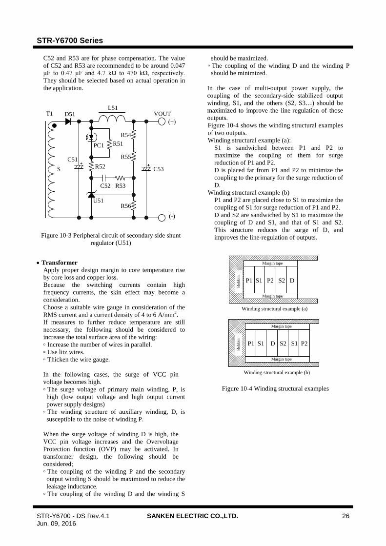
In the case of multi-output power supply, the coupling of the secondary-side stabilized output winding, S1, and the others (S2, S3…) should be maximized to improve the line-regulation of those outputs. Figure 10-4 shows the winding structural examples of two outputs. Winding structural example (a):
S1 is sandwiched between P1 and P2 to maximize the coupling of them for surge reduction of P1 and P2. D is placed far from P1 and P2 to minimize the coupling to the primary for the surge reduction of D.
Winding structural example (b) P1 and P2 are placed close to S1 to maximize the coupling of S1 for surge reduction of P1 and P2. D and S2 are sandwiched by S1 to maximize the coupling of D and S1, and that of S1 and S2. This structure reduces the surge of D, and improves the line-regulation of outputs.
Margin tape
Margin tape
Margin tape
Margin tape
P1 S1 P2 S2 D
P1 S1 D S2 S1 P2
Winding structural example (a)
Winding structural example (b)
Bob
bin
Bob
bin
Figure 10-4 Winding structural examples

STR-Y6700 Series
STR-Y6700 - DS Rev.4.1 SANKEN ELECTRIC CO.,LTD. 27 Jun. 09, 2016
10.2 Transformer Design The design of the transformer is fundamentally the
same as the power transformer of a Ringing Choke Converter (RCC) system: a self-excitation type flyback converter. However, because the duty cycle will change due to the quasi-resonant operations delaying the turn-on, the duty cycle needs to be compensated.
Figure 10-5 shows the quasi-resonant circuit.
T1
S
VINNP NS
LP
CV
VFLY
IDIOFF
VO
C51
VF
C1
D51
P
U1
Figure 10-5 Quasi-resonant circuit
The flyback voltage, VFLY is calculated as follows:
( )FOS
PFLY VV
NNV +×= (12)
where, NP: Primary side number of turns NS: Secondary side number of turns VO: Output voltage VF: Forward voltage drop of D51 The on duty, DON, at the minimum AC input voltage
is calculated as follows:
FLY)MIN(IN
FLYON VV
VD+
= (13)
where, VIN(MIN): C1 voltage at the minimum AC input voltage VFLY: Flyback voltage. The inductance, LP' on the primary side, taking into
consideration the delay time, is calculated using Equation (14).
( )2
VMINON)MIN(IN1
MINO
2
ON)MIN(INP
CπfDVη
f2P
DV'L
×××+
×
×=
(14)
where, VIN(MIN) : C1 voltage at the minimum AC input voltage DON: On-duty at the minimum input voltage PO: maximum output power fMIN: minimum operation frequency η1: transformer efficiency CV: the voltage resonance capacitor connected between the drain and source of the power MOSFET Each parameter, such as the peak drain current, IDP, is
calculated by the following formulas:
VPONDLY C'Lπt ×= (15)
( )ONDLYMINONON tf1D'D ×−= (16)
IN(MIN)2
OIN V
1PI ×=
η (17)
'DI2
ION
INDP
×=
(18)
valueAl'LN P
P‐
=
(19)
( )FLY
FOPS V
VVNN
+×=
(20)
where, tONDLY: Delay time of quasi-resonant operation IIN: Average input current η2: conversion efficiency of the power supply IDP: peak drain current DON’: On-duty after compensation VO: Secondary side output voltage The minimum operation frequency, fMIN, can be
calculated by the Equation (22):
( )2
ON)MIN(INV
P
V2
ON)MIN(IN
1
O
1
O
MINDVC2π
'L
CDV4πη
2Pη
2P
f
××
××++−
=
(21)
Figure 10-6 shows the Example of NI-Limit versus
AL-Value characteristics. Choose the ferrite core that does not saturate and
provides a design margin in consideration of temperature effects and other variations to NI-Limit versus AL-Value characteristics.

STR-Y6700 Series
STR-Y6700 - DS Rev.4.1 SANKEN ELECTRIC CO.,LTD. 28 Jun. 09, 2016
Al-value is calculated by using LP’ and NP. NI is calculated by using Equation (22).
It is recommended that Al-value and NI provide the design margin of 30 % or more for saturation curve of core.
DPP INNI ×= (AT) (22)
where, NP: Primary side number of turns IDP: Peak switching current
NI-
limit
(AT)
Al-value (nH/T2)
Margin : about 30%
Saturation curve
NI
LP’/NP2
Figure 10-6 Example of NI-Limit versus AL-Value characteristics
10.3 PCB Trace Layout and Component Placement
Since the PCB circuit trace design and the component layout significantly affects operation, EMI noise, and power dissipation, the high frequency PCB trace should be low impedance with small loop and wide trace.
In addition, the ground traces affect radiated EMI noise, and wide, short traces should be taken into account.
Figure 10-7 shows the circuit design example.
(1) Main Circuit Trace Layout This is the main trace containing switching currents, and thus it should be as wide trace and small loop as possible. If C1 and the IC are distant from each other, placing a capacitor such as film capacitor (about 0.1 μF and with proper voltage rating) close to the transformer or the IC is recommended to reduce impedance of the high frequency current loop.
(2) Control Ground Trace Layout Since the operation of IC may be affected from the large current of the main trace that flows in control ground trace, the control ground trace should be separated from main trace and connected at a single point grounding of point A in Figure 10-7 as close to the ROCP pin as possible.
(3) VCC Trace Layout This is the trace for supplying power to the IC, and thus it should be as small loop as possible. If C3 and the IC are distant from each other, placing a capacitor such as film capacitor Cf (about 0.1 μF to 1.0 μF) close to the VCC pin and the GND pin is recommended.
(4) ROCP Trace Layout ROCP should be placed as close as possible to the S/OCP pin. The connection between the power ground of the main trace and the IC ground should be at a single point ground (point A in Figure 10-7) which is close to the base of ROCP.
(5) Peripheral components of the IC The components for control connected to the IC should be placed as close as possible to the IC, and should be connected as short as possible to the each pin.
(6) Secondary Rectifier Smoothing Circuit Trace Layout: This is the trace of the rectifier smoothing loop, carrying the switching current, and thus it should be as wide trace and small loop as possible. If this trace is thin and long, inductance resulting from the loop may increase surge voltage at turning off the power MOSFET. Proper rectifier smoothing trace layout helps to increase margin against the power MOSFET breakdown voltage, and reduces stress on the clamp snubber circuit and losses in it.
(7) Thermal Considerations Because the power MOSFET has a positive thermal coefficient of RDS(ON), consider it in thermal design. Since the copper area under the IC and the D/ST pin trace act as a heatsink, its traces should be as wide as possible.

STR-Y6700 Series
STR-Y6700 - DS Rev.4.1 SANKEN ELECTRIC CO.,LTD. 29 Jun. 09, 2016
NF
GN
DFB
/OLP
S/O
CP
VC
C
D/S
T2
1 7542 3 6
BD
C1
D2 R2
C3
T1
D51
C51
D
P
S
PC1
C4
ROCP
CY
CV
A
R3
DZBD
RBD1C5
RBD2
CBD
U1
C2 R1
D1
(1) Main trace should be wide trace and small loop
(6) Main trace of secondary side should be wide trace and small loop
(7)Trace of D/ST pin should be wide for heat release
(2) Control GND trace should be connected at a single point as close to the ROCP as possible
(5)The components connected to the IC should be as close to the IC as possible, and should be connected as short as possible
(3) Loop of the power supply should be small
(4)ROCP should be as close to S/OCP pin as possible.
Figure 10-7 Peripheral circuit example around the IC
STR-Y6700 Series
STR-Y6700 - DS Rev.4.1 SANKEN ELECTRIC CO.,LTD. 30 Jun. 09, 2016
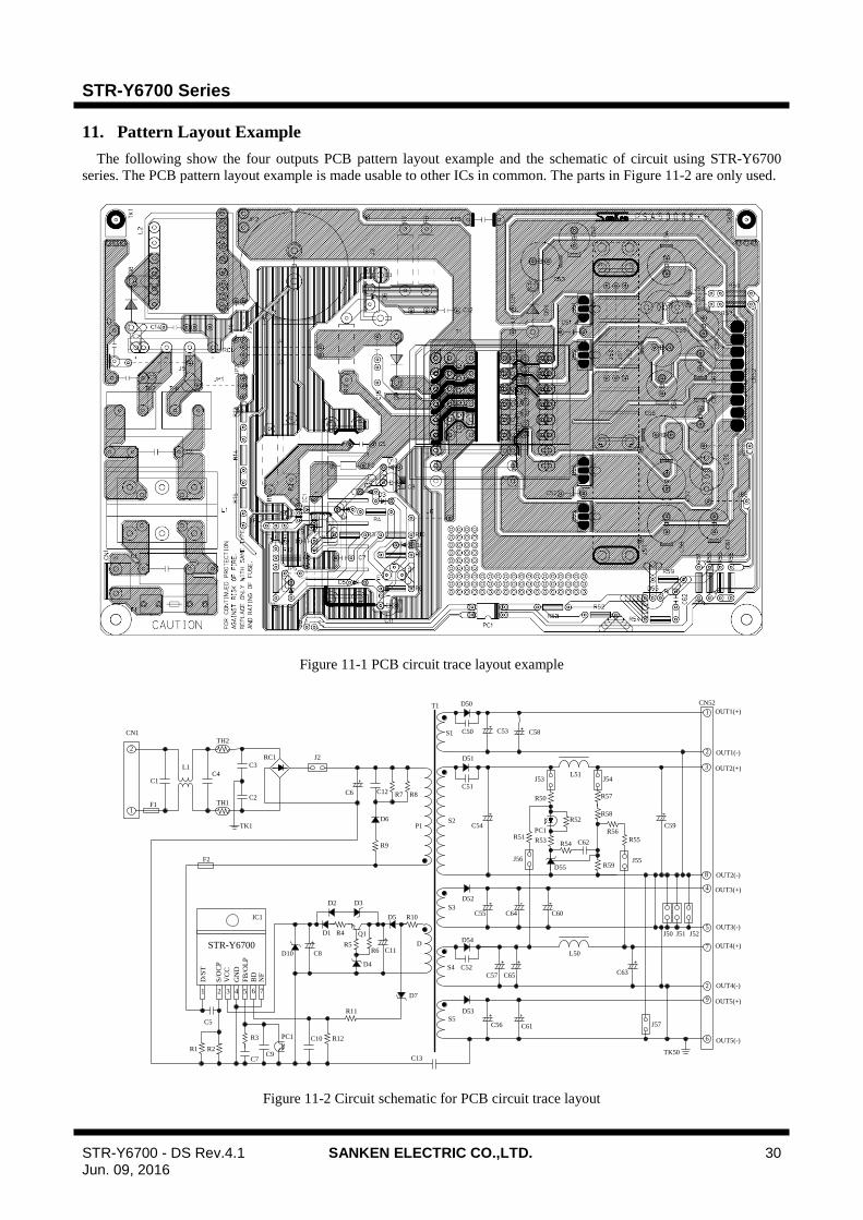
11. Pattern Layout Example The following show the four outputs PCB pattern layout example and the schematic of circuit using STR-Y6700
series. The PCB pattern layout example is made usable to other ICs in common. The parts in Figure 11-2 are only used.
Figure 11-1 PCB circuit trace layout example
3
CN1
C6
T1
D51
R52
D55
D
P1S2
PC1
8
L51
C62R54
F1
2
1
C1
TH2
L1
7
2
C12
C9C7
C11
C5
C13
RC1
D6
D5 R10
R2
R7
D54
C54
C57
R50 R57
R59
R51 R55R56
PC1
C51
C52
C4OUT2(+)
OUT3(-)
C3
C2
TK1
C8
D3
S4
1
2
D50
C53 C58C50
CN52
S5
C59
6
D53
C56
S1
OUT4(+)
OUT5(+)
OUT1(+)
OUT4(-)
OUT5(-)
OUT1(-)
TK50
TH1
J2
R8
R9
BD
GN
DFB
/OLP
S/O
CP
VC
C
D/S
T2
1 6542 3
STR-Y6700
IC1
7
NF
F2
R1R3 C10
D7
R12
R11
D2
Q1R5
D4
D1
D10 R6
R4
R53
R58
J54J53
J56
L50
J55
C65 C63
C61
9
S3
5
D52
C55
OUT3(+)
C64
4
C60
OUT2(-)
J52J50 J51
J57
Figure 11-2 Circuit schematic for PCB circuit trace layout

STR-Y6700 Series
STR-Y6700 - DS Rev.4.1 SANKEN ELECTRIC CO.,LTD. 31 Jun. 09, 2016
12. Reference Design of Power Supply Power supply specification
IC STR-Y6754 Input voltage 85 VAC to 265 VAC Maximum output power 40.4 W Output 1 14 V / 2.6A Output 2 8 V / 0.5 A
Circuit schematic
C2
T1
D52
R52
U51D
P1
S1
PC1
C55R53
F1
C1
L1
C3
C7C6
C5
C4
C9
D1
D5
D6 R3
R2
C54
R51 R54
R56
PC1
C52
OUT2(+)
D51
C53C51
S2 OUT1(+)
R1
BD
GN
DFB
/OLP
S/O
CP
VC
C
D/S
T2
1 6542 3
STR-Y6700
U1
7
NF
R4 C8
DZ1
R6
R5
R55
OUT(-)S3
S4
P2
14V/2.6A
8V/0.5A
D2
D4 D3
Bill of materials
Symbol Part type Ratings(1) Recommended Sanken Parts Symbol Part type Ratings(1) Recommended
Sanken Parts C1 (2) Film, X2 0.1 μF, 275 V D52 Schottky 90 V, 1.5 A EK 19 C2 Electrolytic 220 μF, 400 V DZ1 Zener 22V C3 Ceramic 2200 pF, 630 V F1 Fuse 250 VAC, 3 A C4 Ceramic 100 pF, 2 kV L1 (2) CM inductor 3.3 mH C5 Electrolytic 22 μF, 50V PC1 Photo-coupler PC123or equiv C6 Ceramic 4.7 μF, 16 V R1 (3) Metal oxide 150 kΩ, 1 W C7 (2) Ceramic 4700 pF, 50V R2 (2) General 0.56 Ω, 1 W C8 (2) Ceramic 470 pF, 50V R3 (2) General 15 Ω C9 Ceramic, Y1 2200 pF, 250 V R4 General 47 kΩ
C51 Ceramic 2200 pF, 1 kV R5 (2) General 6.8 kΩ C52 Ceramic Open R6 General 1 kΩ C53 Electrolytic 1000 μF, 50 V R51 General 820 Ω C54 Electrolytic 470 µF, 16 V R52 General 1.5 kΩ C55 Ceramic 0.1 µF R53 (2) General 22 kΩ D1 General 600V, 1A EM01A R54 (2) General 6.8 kΩ D2 General 600V, 1A EM01A R55 General, 1% 39 kΩ D3 General 600V, 1A EM01A R56 General, 1% 10 kΩ
D4 General 600V, 1A EM01A T1 Transformer See the specification
D5 Fast recovery 1000 V, 0.5 A EG01C U1 IC - STR-Y6754
D6 Fast recovery 200 V, 1 A AL01Z U51 Shunt regulator VREF = 2.5 V TL431or equiv
D51 Schottky 150 V, 10 A FMEN-210B (1) Unless otherwise specified, the voltage rating of capacitor is 50 V or less and the power rating of resistor is 1/8 W or less. (2) It is necessary to be adjusted based on actual operation in the application. (3) Resistors applied high DC voltage and of high resistance are recommended to select resistors designed against electromigration or use
combinations of resistors in series for that to reduce each applied voltage, according to the requirement of the application.

STR-Y6700 Series
STR-Y6700 - DS Rev.4.1 SANKEN ELECTRIC CO.,LTD. 32 Jun. 09, 2016
Transformer specification ▫ Primary inductance, LP: 0.95 mH ▫ Core size: EER28L ▫ AL-value: 183 nH/N2 (Center gap of about 0.8 mm) ▫ Winding specification
Winding Symbol Number of turns (T)
Wire diameter (mm) Construction
Primary winding 1 P1 43 1EUW – φ 0.30 Two-layer, solenoid winding
Primary winding 2 P2 29 1EUW – φ 0.30 Single-layer, solenoid winding
Auxiliary winding D 12 TEX – φ 0.23 × 2 Single-layer, Space winding
Output winding 1 S1 5 φ 0.32 × 2 Single-layer, solenoid winding
Output winding 2 S2 3 φ 0.32 × 2 Single-layer, solenoid winding
Output winding 3 S3 5 φ 0.32 × 2 Single-layer, solenoid winding
Output winding 4 S4 3 φ 0.32 × 2 Single-layer, solenoid winding
: Start at this pinCross-section view
Bobbin
D
P1VDC
D/STVCC
GND
14V
S2P2
D
P2
8V
P1S4
OUT1(+)
OUT2(+)
OUT(-)
S1
S3
S1
S2
S3
S4
STR-Y6700 Series
STR-Y6700 - DS Rev.4.1 SANKEN ELECTRIC CO.,LTD. 33 Jun. 09, 2016
IMPORTANT NOTES ● All data, illustrations, graphs, tables and any other information included in this document as to Sanken’s products listed herein (the
“Sanken Products”) are current as of the date this document is issued. All contents in this document are subject to any change without notice due to improvement of the Sanken Products, etc. Please make sure to confirm with a Sanken sales representative that the contents set forth in this document reflect the latest revisions before use.
● The Sanken Products are intended for use as components of general purpose electronic equipment or apparatus (such as home appliances, office equipment, telecommunication equipment, measuring equipment, etc.). Prior to use of the Sanken Products, please put your signature, or affix your name and seal, on the specification documents of the Sanken Products and return them to Sanken. When considering use of the Sanken Products for any applications that require higher reliability (such as transportation equipment and its control systems, traffic signal control systems or equipment, disaster/crime alarm systems, various safety devices, etc.), you must contact a Sanken sales representative to discuss the suitability of such use and put your signature, or affix your name and seal, on the specification documents of the Sanken Products and return them to Sanken, prior to the use of the Sanken Products. The Sanken Products are not intended for use in any applications that require extremely high reliability such as: aerospace equipment; nuclear power control systems; and medical equipment or systems, whose failure or malfunction may result in death or serious injury to people, i.e., medical devices in Class III or a higher class as defined by relevant laws of Japan (collectively, the “Specific Applications”). Sanken assumes no liability or responsibility whatsoever for any and all damages and losses that may be suffered by you, users or any third party, resulting from the use of the Sanken Products in the Specific Applications or in manner not in compliance with the instructions set forth herein.
● In the event of using the Sanken Products by either (i) combining other products or materials therewith or (ii) physically, chemically or otherwise processing or treating the same, you must duly consider all possible risks that may result from all such uses in advance and proceed therewith at your own responsibility.
● Although Sanken is making efforts to enhance the quality and reliability of its products, it is impossible to completely avoid the occurrence of any failure or defect in semiconductor products at a certain rate. You must take, at your own responsibility, preventative measures including using a sufficient safety design and confirming safety of any equipment or systems in/for which the Sanken Products are used, upon due consideration of a failure occurrence rate or derating, etc., in order not to cause any human injury or death, fire accident or social harm which may result from any failure or malfunction of the Sanken Products. Please refer to the relevant specification documents and Sanken’s official website in relation to derating.
● No anti-radioactive ray design has been adopted for the Sanken Products. ● No contents in this document can be transcribed or copied without Sanken’s prior written consent. ● The circuit constant, operation examples, circuit examples, pattern layout examples, design examples, recommended examples, all
information and evaluation results based thereon, etc., described in this document are presented for the sole purpose of reference of use of the Sanken Products and Sanken assumes no responsibility whatsoever for any and all damages and losses that may be suffered by you, users or any third party, or any possible infringement of any and all property rights including intellectual property rights and any other rights of you, users or any third party, resulting from the foregoing.
● All technical information described in this document (the “Technical Information”) is presented for the sole purpose of reference of use of the Sanken Products and no license, express, implied or otherwise, is granted hereby under any intellectual property rights or any other rights of Sanken.
● Unless otherwise agreed in writing between Sanken and you, Sanken makes no warranty of any kind, whether express or implied, including, without limitation, any warranty (i) as to the quality or performance of the Sanken Products (such as implied warranty of merchantability, or implied warranty of fitness for a particular purpose or special environment), (ii) that any Sanken Product is delivered free of claims of third parties by way of infringement or the like, (iii) that may arise from course of performance, course of dealing or usage of trade, and (iv) as to any information contained in this document (including its accuracy, usefulness, or reliability).
● In the event of using the Sanken Products, you must use the same after carefully examining all applicable environmental laws and regulations that regulate the inclusion or use of any particular controlled substances, including, but not limited to, the EU RoHS Directive, so as to be in strict compliance with such applicable laws and regulations.
● You must not use the Sanken Products or the Technical Information for the purpose of any military applications or use, including but not limited to the development of weapons of mass destruction. In the event of exporting the Sanken Products or the Technical Information, or providing them for non-residents, you must comply with all applicable export control laws and regulations in each country including the U.S. Export Administration Regulations (EAR) and the Foreign Exchange and Foreign Trade Act of Japan, and follow the procedures required by such applicable laws and regulations.
● Sanken assumes no responsibility for any troubles, which may occur during the transportation of the Sanken Products including the falling thereof, out of Sanken’s distribution network.
● Although Sanken has prepared this document with its due care to pursue the accuracy thereof, Sanken does not warrant that it is error free and Sanken assumes no liability whatsoever for any and all damages and losses which may be suffered by you resulting from any possible errors or omissions in connection with the contents included herein.
● Please refer to the relevant specification documents in relation to particular precautions when using the Sanken Products, and refer to our official website in relation to general instructions and directions for using the Sanken Products.
DSGN-CEZ-16001