Embed Size (px)
Citation preview
Torridon 2.5” HS Drive Control Module - Technical Manual
Revision 1.9 Quarch Technology Confidential Page 1 of 36
Quarch Technology Ltd
Torridon 2.5” HS Drive Control Module
Technical Manual
For use with:
QTL1177 - Torridon 2.5” SAS/SATA HS Drive Control Module
Using Quarch firmware version 3.5x
Friday, 06 August 2010
Torridon 2.5” HS Drive Control Module - Technical Manual
Revision 1.9 Quarch Technology Confidential Page 2 of 36
Contents Introduction ..........................................................................................................................3
Technical Specifications .........................................................................................................4
Switching Characteristics: ................................................................................................................... 4
Mechanical Characteristics: ................................................................................................................ 6
Control Interfaces ..................................................................................................................7
Timing Limitations .............................................................................................................................. 8
Basic Concepts .......................................................................................................................9
Signal Configuration.......................................................................................................................... 11
Power Up vs. Power Down Timing ................................................................................................... 12
Pin Bounce Modes ............................................................................................................................ 13
Glitch Control .................................................................................................................................... 15
Voltage Measurements ........................................................................................................ 17
Default Startup State ........................................................................................................... 19
Controlling the Module ........................................................................................................ 20
Serial Command Set.......................................................................................................................... 20
SCPI Style Commands ........................................................................................................ 20
Legacy Commands ............................................................................................................. 26
Control Register Map ........................................................................................................... 27
Register Definitions .......................................................................................................................... 29
Source Registers ................................................................................................................ 31
Signal Registers .................................................................................................................. 34
Other Registers .................................................................................................................. 35
Appendix 1 - Signal Names ................................................................................................... 36
Torridon 2.5” HS Drive Control Module - Technical Manual
Revision 1.9 Quarch Technology Confidential Page 3 of 36
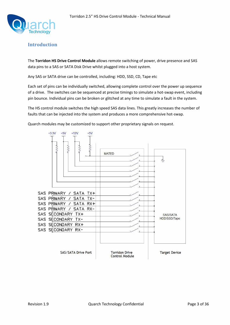
Introduction
The Torridon HS Drive Control Module allows remote switching of power, drive presence and SAS
data pins to a SAS or SATA Disk Drive whilst plugged into a host system.
Any SAS or SATA drive can be controlled, including: HDD, SSD, CD, Tape etc
Each set of pins can be individually switched, allowing complete control over the power up sequence
of a drive. The switches can be sequenced at precise timings to simulate a hot-swap event, including
pin bounce. Individual pins can be broken or glitched at any time to simulate a fault in the system.
The HS control module switches the high speed SAS data lines. This greatly increases the number of
faults that can be injected into the system and produces a more comprehensive hot-swap.
Quarch modules may be customized to support other proprietary signals on request.
Torridon 2.5” HS Drive Control Module - Technical Manual
Revision 1.9 Quarch Technology Confidential Page 4 of 36
Technical Specifications
Switching Characteristics:
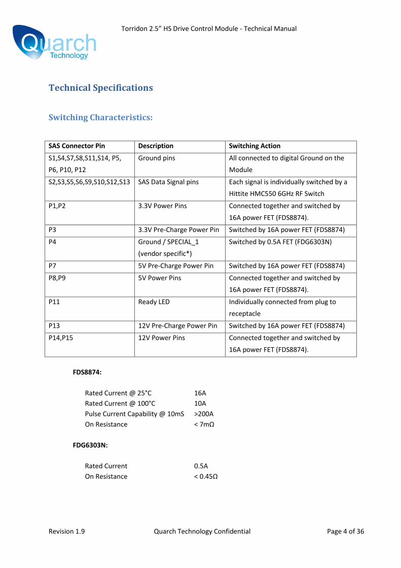
SAS Connector Pin Description Switching Action
S1,S4,S7,S8,S11,S14, P5,
P6, P10, P12
Ground pins All connected to digital Ground on the
Module
S2,S3,S5,S6,S9,S10,S12,S13 SAS Data Signal pins Each signal is individually switched by a
Hittite HMC550 6GHz RF Switch
P1,P2 3.3V Power Pins Connected together and switched by
16A power FET (FDS8874).
P3 3.3V Pre-Charge Power Pin Switched by 16A power FET (FDS8874)
P4 Ground / SPECIAL_1
(vendor specific*)
Switched by 0.5A FET (FDG6303N)
P7 5V Pre-Charge Power Pin Switched by 16A power FET (FDS8874)
P8,P9 5V Power Pins Connected together and switched by
16A power FET (FDS8874).
P11 Ready LED Individually connected from plug to
receptacle
P13 12V Pre-Charge Power Pin Switched by 16A power FET (FDS8874)
P14,P15 12V Power Pins Connected together and switched by
16A power FET (FDS8874).
FDS8874:
Rated Current @ 25°C 16A
Rated Current @ 100°C 10A
Pulse Current Capability @ 10mS >200A
On Resistance < 7mΩ
FDG6303N:
Rated Current 0.5A
On Resistance < 0.45Ω

Torridon 2.5” HS Drive Control Module - Technical Manual
Revision 1.9 Quarch Technology Confidential Page 5 of 36
Power Pin P4 is used as a Mated signal by some vendors, this may also be independently
switched to control drive presence. Subject to volume and lead time, the units may be
customized to suit any proprietary mated circuitry.

Torridon 2.5” HS Drive Control Module - Technical Manual
Revision 1.9 Quarch Technology Confidential Page 6 of 36
Mechanical Characteristics:
The Modules have the same cross section as a 2.5” disk drive, allowing them to fit into any
2.5” drive enclosure.
2.5” Disk Drive
32mm
Torridon
Control
Module
69.85mm
< 15mm
Torridon 2.5” HS Drive Control Module - Technical Manual
Revision 1.9 Quarch Technology Confidential Page 7 of 36
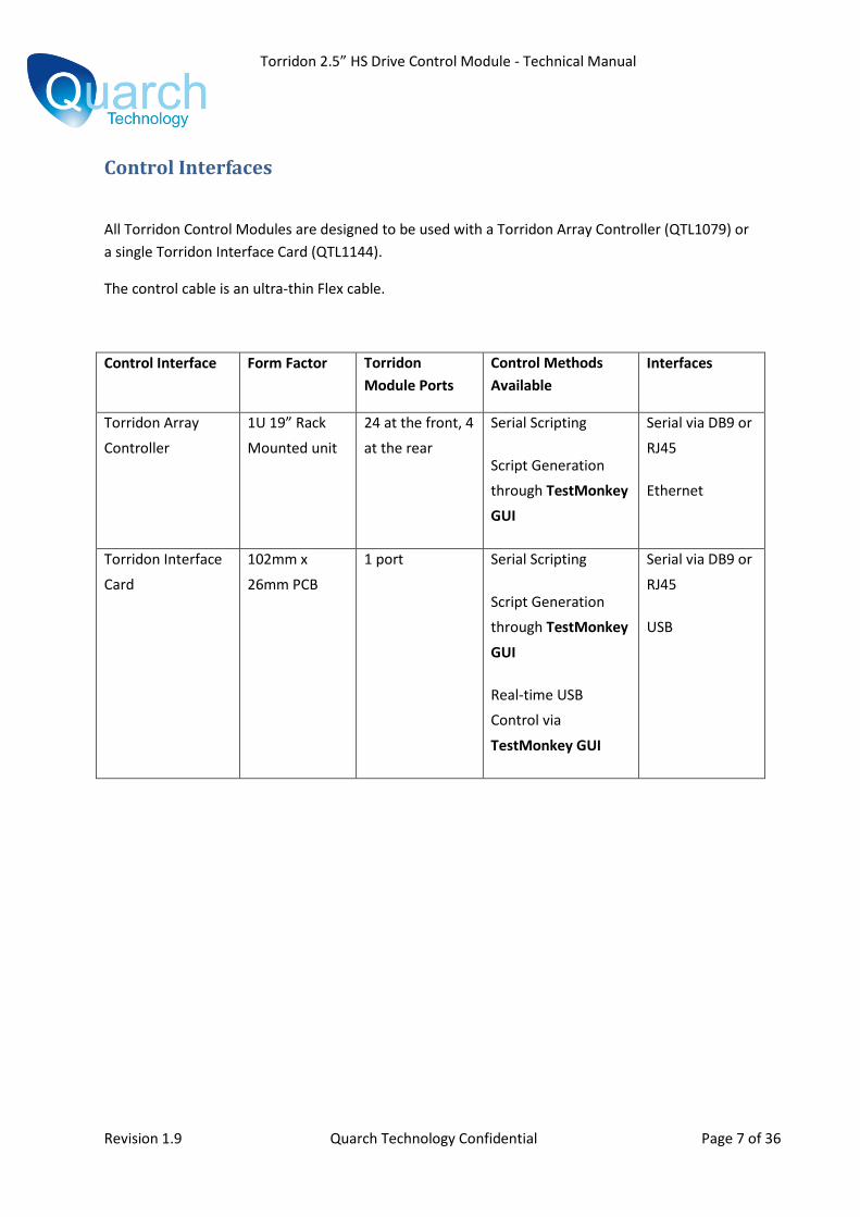
Control Interfaces
All Torridon Control Modules are designed to be used with a Torridon Array Controller (QTL1079) or
a single Torridon Interface Card (QTL1144).
The control cable is an ultra-thin Flex cable.
Control Interface Form Factor Torridon
Module Ports
Control Methods
Available
Interfaces
Torridon Array
Controller
1U 19” Rack
Mounted unit
24 at the front, 4
at the rear
Serial Scripting
Script Generation
through TestMonkey
GUI
Serial via DB9 or
RJ45
Ethernet
Torridon Interface
Card
102mm x
26mm PCB
1 port Serial Scripting
Script Generation
through TestMonkey
GUI
Real-time USB
Control via
TestMonkey GUI
Serial via DB9 or
RJ45
USB
Torridon 2.5” HS Drive Control Module - Technical Manual
Revision 1.9 Quarch Technology Confidential Page 8 of 36
Timing Limitations
When setting some values such an initial delay and pin-bounce, not every value is available. This is
due to multiplier bits that are used to extend the available range. If you are setting these delays via
the SCPI commands then you must be aware of this. If you request a value that cannot be set then
the command will execute but the nearest available value will be used and a warning will be
returned.
Initial Delay: 0-100mS in 1mS increments and 1mS to 1000mS in 10mS increments
Bounce Period: 0-1000uS in 10uS increments and 0-100mS in 1mS increments
NOTE: A set period of 0 will actually use 10uS (the smallest possible value)
Bounce Length: 0-100mS in 1mS increments and 10mS to 1000mS in 10mS increments.
Torridon 2.5” HS Drive Control Module - Technical Manual
Revision 1.9 Quarch Technology Confidential Page 9 of 36
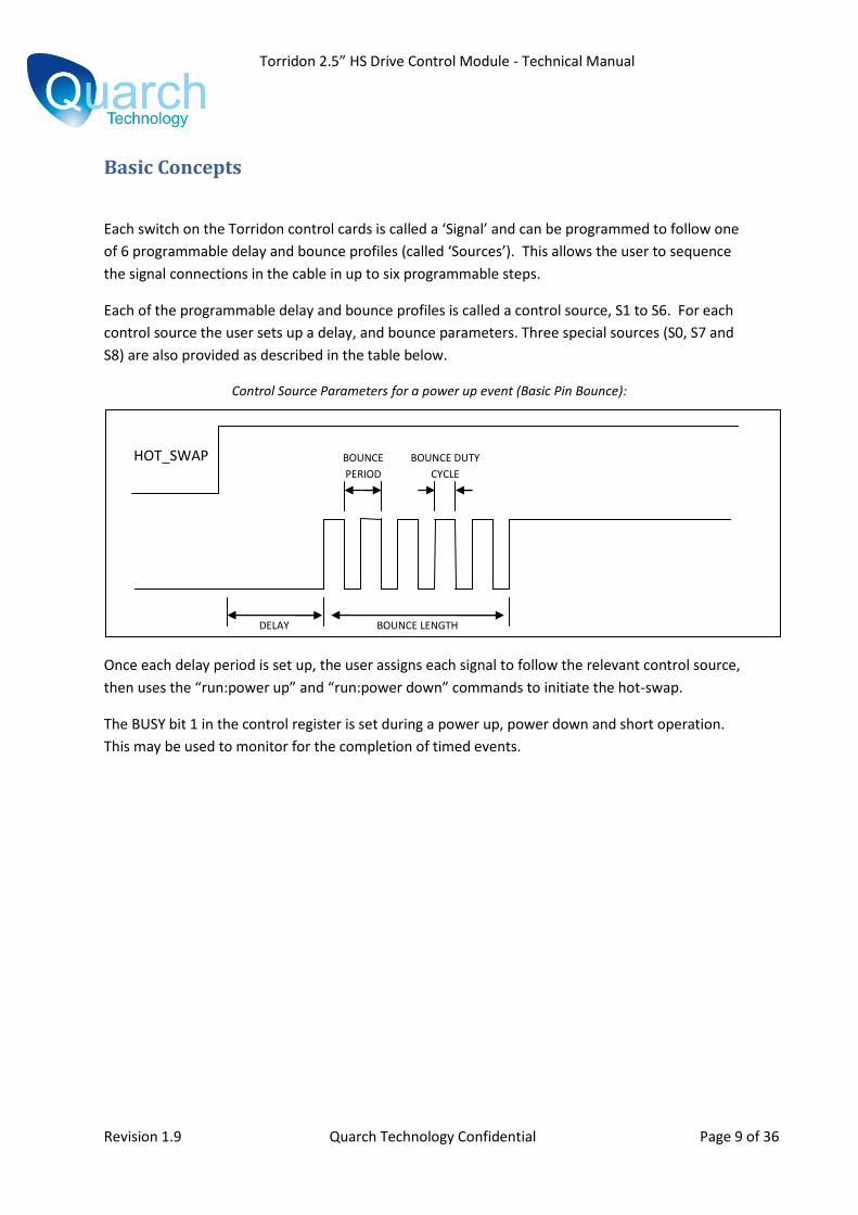
Basic Concepts
Each switch on the Torridon control cards is called a ‘Signal’ and can be programmed to follow one
of 6 programmable delay and bounce profiles (called ‘Sources’). This allows the user to sequence
the signal connections in the cable in up to six programmable steps.
Each of the programmable delay and bounce profiles is called a control source, S1 to S6. For each
control source the user sets up a delay, and bounce parameters. Three special sources (S0, S7 and
S8) are also provided as described in the table below.
Control Source Parameters for a power up event (Basic Pin Bounce):
Once each delay period is set up, the user assigns each signal to follow the relevant control source,
then uses the “run:power up” and “run:power down” commands to initiate the hot-swap.
The BUSY bit 1 in the control register is set during a power up, power down and short operation.
This may be used to monitor for the completion of timed events.
DELAY
BOUNCE
PERIOD
HOT_SWAP
BOUNCE LENGTH
BOUNCE DUTY
CYCLE
Torridon 2.5” HS Drive Control Module - Technical Manual
Revision 1.9 Quarch Technology Confidential Page 10 of 36
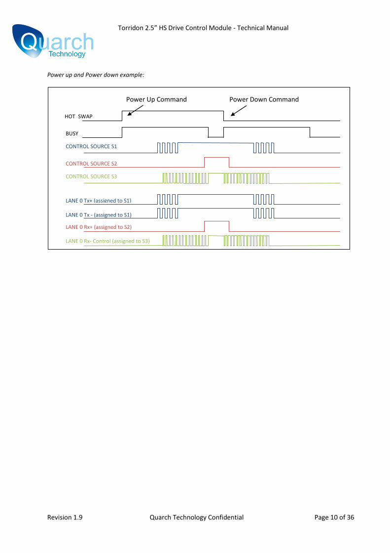
Power up and Power down example:
HOT_SWAP
CONTROL SOURCE S1
CONTROL SOURCE S2
CONTROL SOURCE S3
BUSY
LANE 0 Tx+ (assigned to S1)
LANE 0 Tx - (assigned to S1)
LANE 0 Rx+ (assigned to S2)
LANE 0 Rx- Control (assigned to S3)
Power Up Command Power Down Command
Torridon 2.5” HS Drive Control Module - Technical Manual
Revision 1.9 Quarch Technology Confidential Page 11 of 36
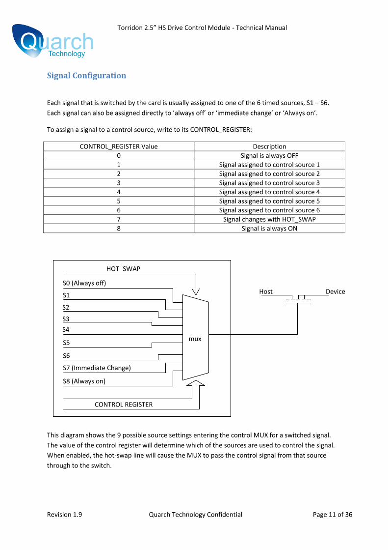
Signal Configuration
Each signal that is switched by the card is usually assigned to one of the 6 timed sources, S1 – S6.
Each signal can also be assigned directly to ’always off’ or ‘immediate change’ or ‘Always on’.
To assign a signal to a control source, write to its CONTROL_REGISTER:
CONTROL_REGISTER Value Description
0 Signal is always OFF
1 Signal assigned to control source 1
2 Signal assigned to control source 2
3 Signal assigned to control source 3
4 Signal assigned to control source 4
5 Signal assigned to control source 5
6 Signal assigned to control source 6
7 Signal changes with HOT_SWAP
8 Signal is always ON
This diagram shows the 9 possible source settings entering the control MUX for a switched signal.
The value of the control register will determine which of the sources are used to control the signal.
When enabled, the hot-swap line will cause the MUX to pass the control signal from that source
through to the switch.
HOT_SWAP
S2
S3
S4
S5
S6
S7 (Immediate Change)
S0 (Always off)
S1
CONTROL REGISTER
Host
mux
S8 (Always on)
Device
Torridon 2.5” HS Drive Control Module - Technical Manual
Revision 1.9 Quarch Technology Confidential Page 12 of 36
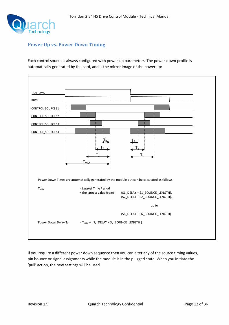
Power Up vs. Power Down Timing
Each control source is always configured with power-up parameters. The power-down profile is
automatically generated by the card, and is the mirror image of the power up:
If you require a different power down sequence then you can alter any of the source timing values,
pin bounce or signal assignments while the module is in the plugged state. When you initiate the
‘pull’ action, the new settings will be used.
BUSY
CONTROL SOURCE S1
CONTROL_SOURCE S2
CONTROL_SOURCE S3
CONTROL_SOURCE S4
HOT_SWAP
T1
T2
T3
T1
T2
T3
Power Down Times are automatically generated by the module but can be calculated as follows:
TMAX = Largest Time Period = the largest value from: (S1_DELAY + S1_BOUNCE_LENGTH), (S2_DELAY + S2_BOUNCE_LENGTH), up to (S6_DELAY + S6_BOUNCE_LENGTH) Power Down Delay TX = TMAX – ( SX_DELAY + SX_BOUNCE_LENGTH )
TMAX
Torridon 2.5” HS Drive Control Module - Technical Manual
Revision 1.9 Quarch Technology Confidential Page 13 of 36
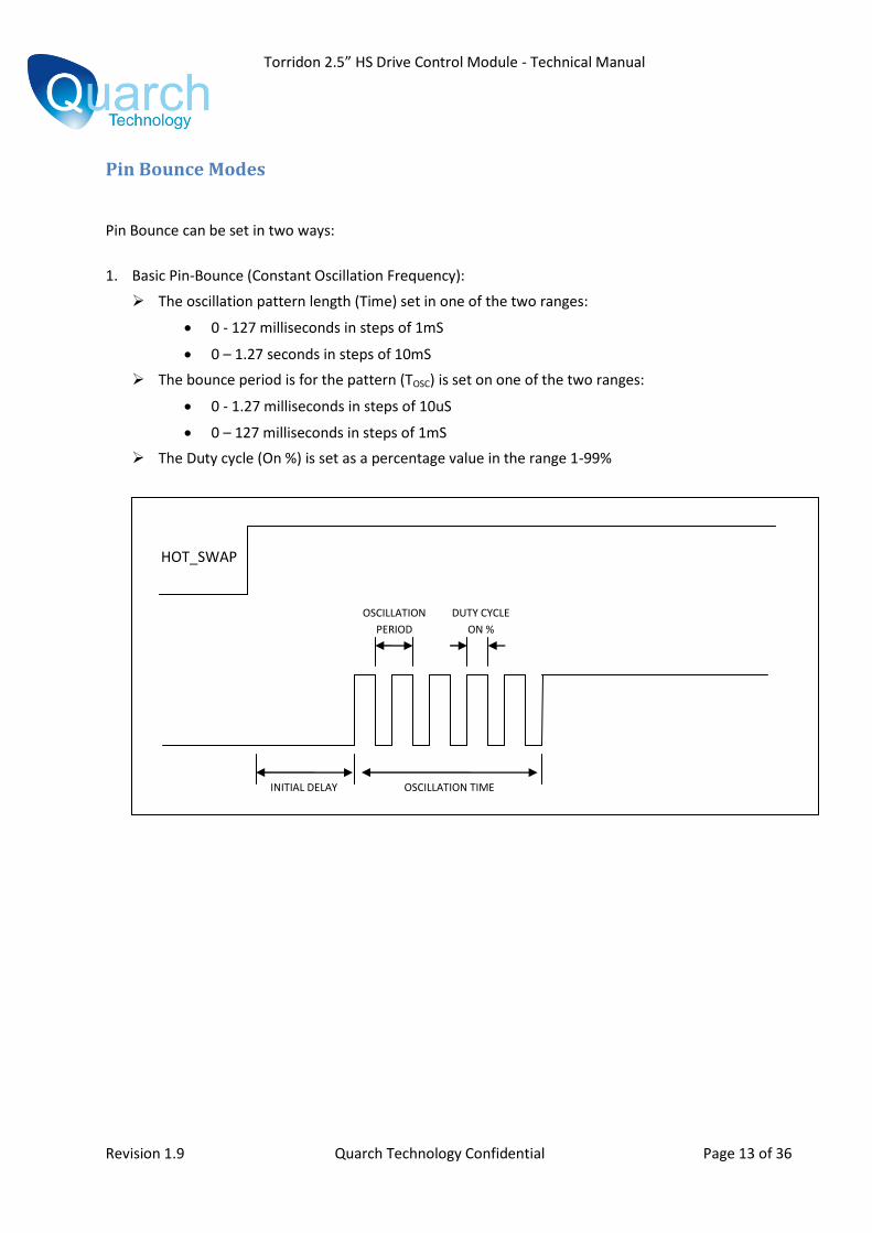
Pin Bounce Modes
Pin Bounce can be set in two ways:
1. Basic Pin-Bounce (Constant Oscillation Frequency):
The oscillation pattern length (Time) set in one of the two ranges:
0 - 127 milliseconds in steps of 1mS
0 – 1.27 seconds in steps of 10mS
The bounce period is for the pattern (TOSC) is set on one of the two ranges:
0 - 1.27 milliseconds in steps of 10uS
0 – 127 milliseconds in steps of 1mS
The Duty cycle (On %) is set as a percentage value in the range 1-99%
INITIAL DELAY
OSCILLATION
PERIOD
HOT_SWAP
OSCILLATION TIME
DUTY CYCLE
ON %
Torridon 2.5” HS Drive Control Module - Technical Manual
Revision 1.9 Quarch Technology Confidential Page 14 of 36
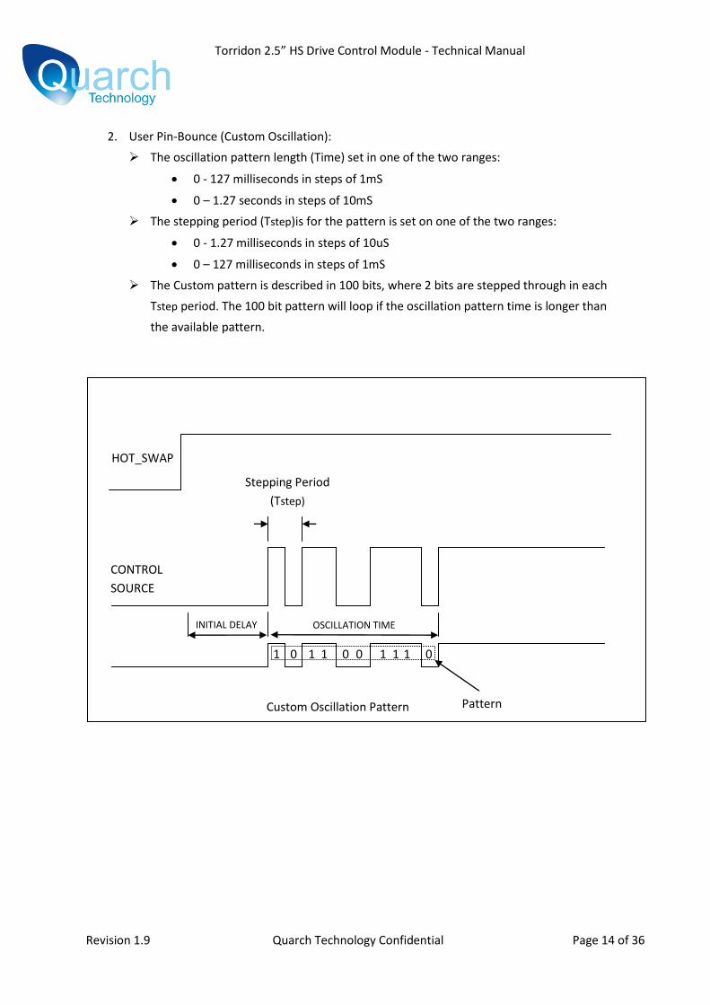
2. User Pin-Bounce (Custom Oscillation):
The oscillation pattern length (Time) set in one of the two ranges:
0 - 127 milliseconds in steps of 1mS
0 – 1.27 seconds in steps of 10mS
The stepping period (Tstep)is for the pattern is set on one of the two ranges:
0 - 1.27 milliseconds in steps of 10uS
0 – 127 milliseconds in steps of 1mS
The Custom pattern is described in 100 bits, where 2 bits are stepped through in each
Tstep period. The 100 bit pattern will loop if the oscillation pattern time is longer than
the available pattern.
INITIAL DELAY
Stepping Period
(Tstep)
Custom Oscillation Pattern
1 0 1 1 1 1 1 0 0 0
HOT_SWAP
CONTROL
SOURCE
Pattern
OSCILLATION TIME

Torridon 2.5” HS Drive Control Module - Technical Manual
Revision 1.9 Quarch Technology Confidential Page 15 of 36
Glitch Control
Any control signal may be glitched for a pre-determined length of time using the glitch generator
logic.
Each Signal Control register contains a “GLITCH_ENABLE” bit which determines whether the glitch
logic will affect that signal. The GLITCH ENABLE bit, defaults to off, so any glitches will have no effect
unless explicitly set to do so.
Glitches will invert the current state of the switched signal. Therefore if a switch is currently OFF, a
glitch will turn it ON, and if the switch is ON, it will turn OFF.
Glitches may be applied in 3 modes: Glitch Once:
A single glitch is generated when the RUN:GLITch ONCE command is executed The length of the glitch is determined by using the GLITch:SETup command or the GLITch:MULTiplier and GLITch:LENgth commands.
PULSE LENGTH = GLITch:MULTiplier x GLITch:LENgth
Repeated use of the RUN:GLITch: ONCE command will generate multiple glitches, it is not necessary to use the RUN:GLITch OFF command after a single glitch.
Glitch Cycle:
A sequence of glitches is generated when the RUN:GLITch CYCLE command is executed, and continues until RUN:GLITch OFF is executed. The length of the glitch is determined by using the GLITch:SETup command or the GLITch:MULTiplier and GLITch:LENgth commands:
PULSE LENGTH = GLITch:MULTiplier x GLITch:LENgth The length of time between each glitch pulse is determined by the GLITch:MULTiplier and GLITch:CYCLE commands:
OFF TIME = GLITch:MULTiplier x GLITch:CYCLE

Torridon 2.5” HS Drive Control Module - Technical Manual
Revision 1.9 Quarch Technology Confidential Page 16 of 36
Glitch PRBS:
A pseudo random sequence of glitches is generated when the RUN:GLITch PRBS command is executed, and continues until RUN:GLITch OFF is executed. The length of the glitch is determined by using the GLITch:SETup command or the GLITch:MULTiplier and GLITch:LENGTH commands:
PULSE LENGTH = GLITch:MULTiplier x GLITch:LENgth
The number of glitches in a set length of time is determined by the GLITch:PRBS command. A value of 2 will result in glitches at a ratio of 1:2 (the line will be in a glitched state 50% of the time), whilst a value of 256 will produce glitches in a ratio of 1:256.
Torridon 2.5” HS Drive Control Module - Technical Manual
Revision 1.9 Quarch Technology Confidential Page 17 of 36
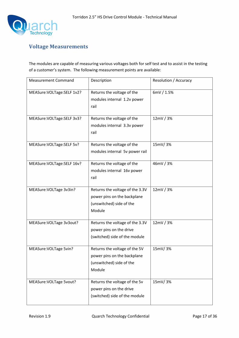
Voltage Measurements
The modules are capable of measuring various voltages both for self test and to assist in the testing
of a customer’s system. The following measurement points are available:
Measurement Command Description Resolution / Accuracy
MEASure:VOLTage:SELF 1v2? Returns the voltage of the
modules internal 1.2v power
rail
6mV / 1.5%
MEASure:VOLTage:SELF 3v3? Returns the voltage of the
modules internal 3.3v power
rail
12mV / 3%
MEASure:VOLTage:SELF 5v? Returns the voltage of the
modules internal 5v power rail
15mV/ 3%
MEASure:VOLTage:SELF 16v? Returns the voltage of the
modules internal 16v power
rail
46mV / 3%
MEASure:VOLTage 3v3in? Returns the voltage of the 3.3V
power pins on the backplane
(unswitched) side of the
Module
12mV / 3%
MEASure:VOLTage 3v3out? Returns the voltage of the 3.3V
power pins on the drive
(switched) side of the module
12mV / 3%
MEASure:VOLTage 5vin? Returns the voltage of the 5V
power pins on the backplane
(unswitched) side of the
Module
15mV/ 3%
MEASure:VOLTage 5vout? Returns the voltage of the 5v
power pins on the drive
(switched) side of the module
15mV/ 3%

Torridon 2.5” HS Drive Control Module - Technical Manual
Revision 1.9 Quarch Technology Confidential Page 18 of 36
MEASure:VOLTage 12vin? Returns the voltage of the 12V
power pins on the backplane
(unswitched) side of the
Module
46mV / 3%
MEASure:VOLTage 12vout? Returns the voltage of the 12v
power pins on the drive
(switched) side of the module
46mV / 3%
Torridon 2.5” HS Drive Control Module - Technical Manual
Revision 1.9 Quarch Technology Confidential Page 19 of 36
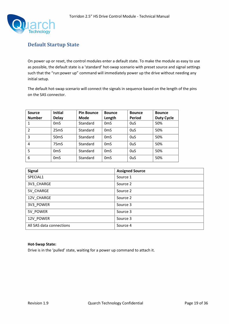
Default Startup State
On power up or reset, the control modules enter a default state. To make the module as easy to use
as possible, the default state is a ‘standard’ hot-swap scenario with preset source and signal settings
such that the “run:power up” command will immediately power up the drive without needing any
initial setup.
The default hot-swap scenario will connect the signals in sequence based on the length of the pins
on the SAS connector.
Source Number
Initial Delay
Pin Bounce Mode
Bounce Length
Bounce Period
Bounce Duty Cycle
1 0mS Standard 0mS 0uS 50%
2 25mS Standard 0mS 0uS 50%
3 50mS Standard 0mS 0uS 50%
4 75mS Standard 0mS 0uS 50%
5 0mS Standard 0mS 0uS 50%
6 0mS Standard 0mS 0uS 50%
Signal Assigned Source
SPECIAL1 Source 1
3V3_CHARGE Source 2
5V_CHARGE Source 2
12V_CHARGE Source 2
3V3_POWER Source 3
5V_POWER Source 3
12V_POWER Source 3
All SAS data connections Source 4
Hot-Swap State:
Drive is in the ‘pulled’ state, waiting for a power up command to attach it.
Torridon 2.5” HS Drive Control Module - Technical Manual
Revision 1.9 Quarch Technology Confidential Page 20 of 36
Controlling the Module
The Drive Control Module can be controlled either by:
Serial ASCII terminal (such as HyperTerminal)
This is normally used with scripted commands to automate a series of tests. The commands
are normally generated by a script or user code (PERL, TCL, C, C# or similar).
USB
Quarch’s TestMonkey application can control a single module via USB, this allows simple
graphical control of the module.
Serial Command Set
When connected via a serial terminal, the drive modules have a simple command line interface
SCPI Style Commands
These commands are based on the SCPI style control system that is used by many manufacturers of
test instruments. The entire SCPI specification has NOT been implemented but the command
structure will be very familiar to anyone who has used it before.
SCPI commands are NOT case sensitive
SCPI commands are in a hierarchy separated by ‘:’ (LEVel1:LEVel2:LEVel3)
Most words have a short form (e.g. ‘register’ shortens to ‘reg’). This will be documented as
REGister, where the short form is shown in capitals.
Some commands take parameters. These are separated by spaces after the main part of the
command (e.g. “meas:volt:self 3v3?” Obtains the 3v3 self test measurement)
Query commands that return a value all have a ‘?’ on the end
Commands with a preceding ‘*’ are basic control commands, found on all devices
Commands that do not return a particular value will return “OK” or “FAIL”. Unless disabled,
the fail response will also append a text description for the failure if it can be determined.
# [comments]
Any line beginning with a # character is ignored as a comment. This allows commenting
of scripts for use with the module.
*RST
Triggers a reset, the controller will behave as if it had just been powered on

Torridon 2.5” HS Drive Control Module - Technical Manual
Revision 1.9 Quarch Technology Confidential Page 21 of 36
*CLR
Clear the terminal window and displays the normal start screen. Also runs the internal
self test. The same action can be performed by pressing return on a blank line.
*IDN?
Displays a standard set of information, identifying the device. An example return is
shown below
Family: Torridon System [The parent family of the device]
Name: 2.5” HS Drive Control Module [The name of the device]
Part#: QTL1177-01 [The part number of the hardware]
Processor: QTL1183-01,3.50 [Part# and version of firmware]
Bootloader: QTL1170-01,1.01 [Part# and version of bootloader]
FPGA 1: 1.4 [Version of FPGA core]
*TST?
Runs a set of standard tests to confirm the device is operating correctly, these tests are
also performed at start up. Returns ‘OK’ or ‘FAIL’ followed by a list of errors that
occurred, each on a new line.
CONFig:TERM USER
Sets the terminal response mode to the default ‘User’ setting. This is intended for use
with HyperTerminal or similar and manually typed commands
CONFig:TERM SCRIPT
Sets the terminal response mode for easier parsing. Especially useful from a UNIX/LINUX
based system. Characters send from the PC are not echoed by the device and a
<CR><LF> is send after the cursor to force a flush of the USART buffer.
CONFig:TERM ? Returns the current terminal mode CONFig:MESSages [SHORt|USER]
CONFig:MESSages?
Gets or sets the mode for messages that are returned to the user’s terminal
Short: Only a “FAIL” or “OK” will be returned
User: Full error messages are returned to the user on failure

Torridon 2.5” HS Drive Control Module - Technical Manual
Revision 1.9 Quarch Technology Confidential Page 22 of 36
REGister:READ [0xAA]
Returns the value of the register with address [0xAA]. [0xAA] should be in hex format
and preceded by the suffix “0x”. e.g. “0x6D” or “0x006D”. The value is returned in the
same form as the address.
REGister:DUMP [0xA1] [0xA2]
Returns the value of each register in a range, starting at the first register address, up to
the second. *0xA1+ and *0xA2+ should be in hex format and preceded by the suffix “0x”.
Each data value will be returned on a new line.
REGister:WRITe [0xAAAA] [0xDDDD]
Writes the byte [0xDD] to register [0xAAAA], both [0xDDDD] and [0xAAAA] should be in
hex format and preceded by the suffix “0x”. The command returns “OK” or “FAIL”.
RUN:POWer [UP|DOWN]
Powers the drive up or down. This is done by changing the HOT_SWAP bit, register 0x00
bit 0. This is the master control for all switches on the card. The same action can be
performed by writing this bit directly.
The command will fail if you order a power up when the drive is already in the plugged
state and vice-versa as the action cannot be performed.
The “OK” response will be returned as soon as the hot-swap event has begun. If your
timing sequence is very long you may have to poll the BUSY bit to check when it has
completed.
MEASure:VOLTage [3v3in?|3v3out?|5vin?|5vout?|12vin?|12vout?]
Returns the voltage on the specified rail in mV. Vin refers to the upstream or host side
of the card, and Vout refers to the switched, drive side. Values are returned in the form
“3300mV”.
MEAS:VOLTage:SELF [1v2?|3v3?|5v?|16v?]
Returns the self test voltages. These are measurements of voltage rails required for
correct operation of the module. The values are returned in the form “5000mV”
SOURce:[1-6|ALL]:SETup [#1] [#2] [#3] [#4]
Sets up the source in a single command. All parameters are positive decimal numbers:
#1 = Initial delay (mS)
Torridon 2.5” HS Drive Control Module - Technical Manual
Revision 1.9 Quarch Technology Confidential Page 23 of 36
#2 = Bounce length (mS)
#3 = Bounce Period (uS)
#4 = Duty Cycle (%)
SOURce:[1-6|ALL]:DELAY [#ms]
SOURce:[1-6|ALL]:DELAY?
Sets the initial delay of a source in mS. The delay is entered as a decimal number with no
units. E.g. “Source:1:delay 300”.
SOURce:[1-6|ALL]:BOUNce:LENgth [#ms]
SOURce:[1-6|ALL]:BOUNce:LENgth?
Sets the length of the pin bounce in mS. The delay is entered as a decimal number with
no units. E.g. “Sour:2:boun:len 50”. Due to hardware limitations, the exact value you
request may not be available. In this case, the nearest value will be used. See “Timing
Limitations” for details.
SOURce:[1-6|ALL]:BOUNce:PERiod [#us]
SOURce:[1-6|ALL]:BOUNce:PERiod?
Sets the bounce period of the pin bounce in uS. The value is entered as a decimal
number with no units. E.g. “Sour:6:boun:period 300”. Due to hardware limitations, the
exact value you request may not be available. In this case, the nearest value will be used.
See “Timing Limitations” for details.
SOURce:[1-6|ALL]:BOUNce:DUTY [#%]
SOURce:[1-6|ALL]:BOUNce:DUTY?
Sets the duty cycle of the pin bounce as a %. The value is entered as a decimal number
with no units. E.g. “source:3:bounce:duty 50”.
SOURce:[1-6|ALL]:BOUNce:CLEAR
Removes any pin bounce from the source and sets all bounce settings to default values. See “Startup State” for details for the default settings.
SIGnal:[SIG_NAME|ALL]:SETup [#num] SIGnal:[SIG_NAME|ALL]:SOURce [#num]
Sets a given signal to a numbered timing source (0-7). SIGNAL_NAME is one of the following signals that can be switched by the drive control module:
Torridon 2.5” HS Drive Control Module - Technical Manual
Revision 1.9 Quarch Technology Confidential Page 24 of 36
12V_POWER 12V_CHARGE 5V_POWER 5V_CHARGE 3V3_POWER 3V3_CHARGE SPECIAL1 (Ground 7, used as mated by some manufacturers)
PRI_OUT_PL (High speed SAS data. ‘OUT’ is Tx from the backplane)
PRI_OUT_MN
PRI_IN_PL
PRI_IN_MN
SEC_OUT_PL
SEC_OUT_MN
SEC_IN_PL
SEC_IN_MN
SIGnal:[SIG_NAME|ALL]:GLITch:ENAble [ON|OFF] SIGnal:[SIG_NAME|ALL]:GLITch:ENAble?
Enables a signal for glitching. If this in on, the signal will be glitched whenever the glitch controller is in use. Multiple signals may be set for glitch at the same time.
RUN:GLITch ONCE Triggers a single glitch RUN:GLITch CYCLE Starts a cycling glitch sequence RUN:GLITch PRBS Starts a PRBS glitch sequence RUN:GLITch:STOP Stops any running sequence of glitching GLITch:SETup [MULTIPLIER_STEP] [#1] Sets up the glitch time in a single command. MULTIPLIER_STEP = One of the multiplier step values from the command below #1 = The length of the glitch in steps

Torridon 2.5” HS Drive Control Module - Technical Manual
Revision 1.9 Quarch Technology Confidential Page 25 of 36
GLITch:MULTiplier [50ns|500sn|5us|50us|500us|5ms|50ms|500ms] GLITch:MULTiplier?
Sets the multiplier step value for the glitch time. A wide range or multipliers are supplied to allow a full range of glitch lengths. This factor is combined with the ‘glitch length’ value to give the actual glitch time
GLITch:LENgth [#num] GLITch:LENgth?
Sets the length of the glitch. This is multiplied up by the ‘glitch multiplier’ to give the
final time of the glitch
GLITch:CYCLE [#num]
Sets the cycle counter for cycling repeat glitches
GLITch:PRBS [2|4|8|16|32|64|128|256]
Sets the PRBS rate for Pseudo Random repeat glitching
Torridon 2.5” HS Drive Control Module - Technical Manual
Revision 1.9 Quarch Technology Confidential Page 26 of 36
Legacy Commands
The following legacy commands are still supported from previous firmware versions to ensure
backward compatibility:
voltage [3v3in|3v3out|5vin|5vout|12vin|12vout]
Returns the voltage on the specified rail in mV. Vin refers to the upstream or host side
of the card, and Vout refers to the switched, drive side.
power [up|down]
Powers the drive up or down. This is done by changing the HOT_SWAP bit, register 0x00
bit 0. This is the master control for all switches on the card. The same action can be
performed by writing this bit directly.
The command will fail if you order a power up when the drive is already in the plugged
state and vice-versa as the action cannot be performed.
The “OK” response will be returned as soon as the hot-swap event has begun. If your
timing sequence is very long you may have to poll the BUSY bit to check when it has
completed.
write [0xAA] [0xDD]
Writes the byte [0xDD] to register [0xAA], both [0xDD] and [0xAA] should be in hex
format and preceded by the suffix “0x”. The command returns “OK” or “FAIL”.
read [0xAA]
Returns the value of the register with address [0xAA]. [0xAA] should be in hex format
and preceded by the suffix “0x”. e.g. “0x6D”. The value is returned in the same form as
the address.
read [0xA1] to [0xA2]
Returns the value of each register in a range, starting at the first register address, up to
the second. *0xA1+ and *0xA2+ should be in hex format and preceded by the suffix “0x”.
Each data value will be returned on a new line.
Torridon 2.5” HS Drive Control Module - Technical Manual
Revision 1.9 Quarch Technology Confidential Page 27 of 36
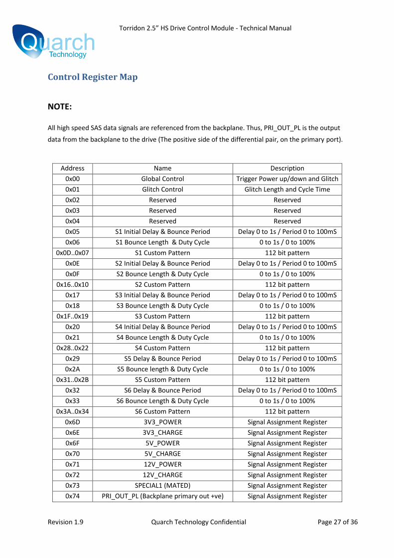
Control Register Map
NOTE: All high speed SAS data signals are referenced from the backplane. Thus, PRI_OUT_PL is the output
data from the backplane to the drive (The positive side of the differential pair, on the primary port).
Address Name Description
0x00 Global Control Trigger Power up/down and Glitch
0x01 Glitch Control Glitch Length and Cycle Time
0x02 Reserved Reserved
0x03 Reserved Reserved
0x04 Reserved Reserved
0x05 S1 Initial Delay & Bounce Period Delay 0 to 1s / Period 0 to 100mS
0x06 S1 Bounce Length & Duty Cycle 0 to 1s / 0 to 100%
0x0D..0x07 S1 Custom Pattern 112 bit pattern
0x0E S2 Initial Delay & Bounce Period Delay 0 to 1s / Period 0 to 100mS
0x0F S2 Bounce Length & Duty Cycle 0 to 1s / 0 to 100%
0x16..0x10 S2 Custom Pattern 112 bit pattern
0x17 S3 Initial Delay & Bounce Period Delay 0 to 1s / Period 0 to 100mS
0x18 S3 Bounce Length & Duty Cycle 0 to 1s / 0 to 100%
0x1F..0x19 S3 Custom Pattern 112 bit pattern
0x20 S4 Initial Delay & Bounce Period Delay 0 to 1s / Period 0 to 100mS
0x21 S4 Bounce Length & Duty Cycle 0 to 1s / 0 to 100%
0x28..0x22 S4 Custom Pattern 112 bit pattern
0x29 S5 Delay & Bounce Period Delay 0 to 1s / Period 0 to 100mS
0x2A S5 Bounce length & Duty Cycle 0 to 1s / 0 to 100%
0x31..0x2B S5 Custom Pattern 112 bit pattern
0x32 S6 Delay & Bounce Period Delay 0 to 1s / Period 0 to 100mS
0x33 S6 Bounce Length & Duty Cycle 0 to 1s / 0 to 100%
0x3A..0x34 S6 Custom Pattern 112 bit pattern
0x6D 3V3_POWER Signal Assignment Register
0x6E 3V3_CHARGE Signal Assignment Register
0x6F 5V_POWER Signal Assignment Register
0x70 5V_CHARGE Signal Assignment Register
0x71 12V_POWER Signal Assignment Register
0x72 12V_CHARGE Signal Assignment Register
0x73 SPECIAL1 (MATED) Signal Assignment Register
0x74 PRI_OUT_PL (Backplane primary out +ve) Signal Assignment Register

Torridon 2.5” HS Drive Control Module - Technical Manual
Revision 1.9 Quarch Technology Confidential Page 28 of 36
0x75 PRI_OUT_MN (Backplane primary out -ve) Signal Assignment Register
0x76 PRI_IN_PL (Backplane primary in +ve) Signal Assignment Register
0x77 PRI_IN_MN (Backplane primary in -ve) Signal Assignment Register
0x78 SEC_OUT_PL (Backplane secondary out +ve) Signal Assignment Register
0x79 SEC_OUT_MN (Backplane secondary out -ve) Signal Assignment Register
0x7a SEC_IN_PL (Backplane secondary in +ve) Signal Assignment Register
0x7b SEC_IN_MN (Backplane secondary in -ve) Signal Assignment Register
Torridon 2.5” HS Drive Control Module - Technical Manual
Revision 1.9 Quarch Technology Confidential Page 29 of 36
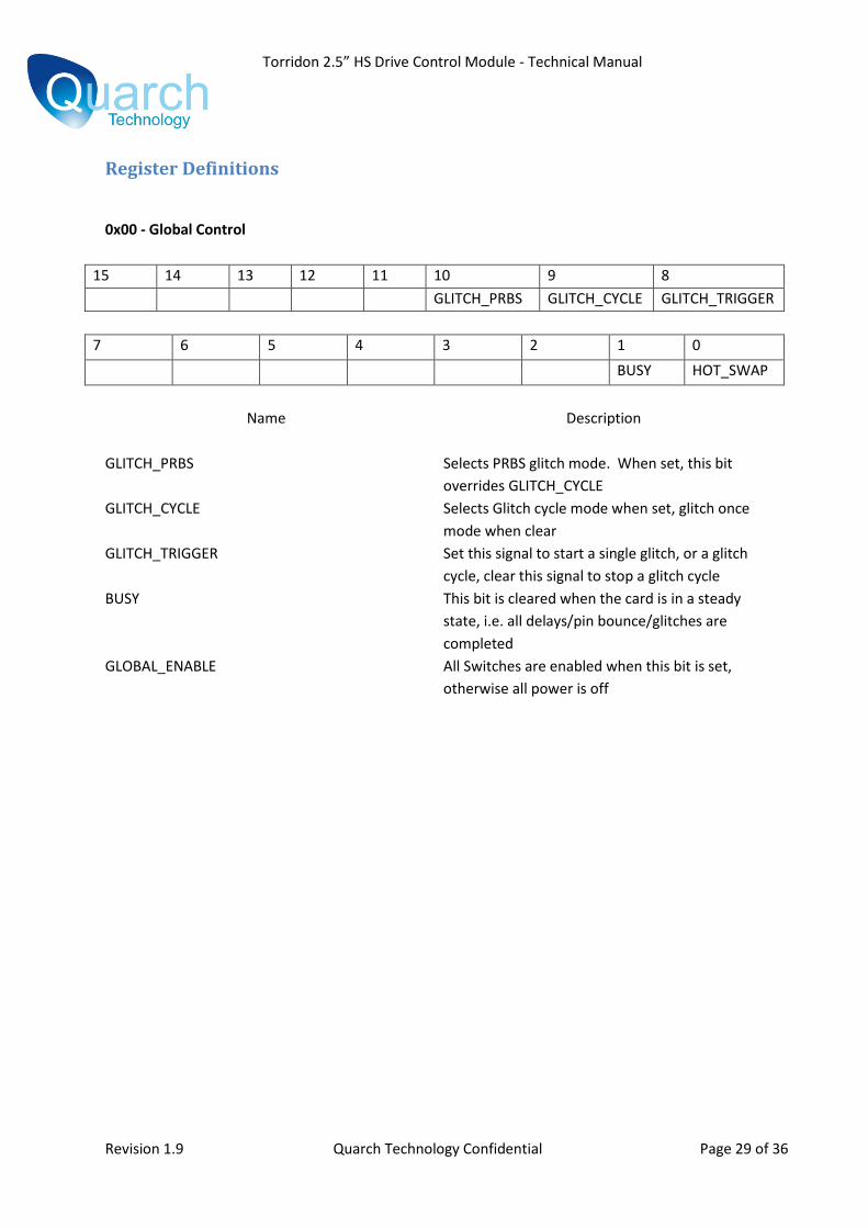
Register Definitions
0x00 - Global Control
15 14 13 12 11 10 9 8
GLITCH_PRBS GLITCH_CYCLE GLITCH_TRIGGER
7 6 5 4 3 2 1 0
BUSY HOT_SWAP
Name Description
GLITCH_PRBS Selects PRBS glitch mode. When set, this bit
overrides GLITCH_CYCLE
GLITCH_CYCLE Selects Glitch cycle mode when set, glitch once
mode when clear
GLITCH_TRIGGER Set this signal to start a single glitch, or a glitch
cycle, clear this signal to stop a glitch cycle
BUSY This bit is cleared when the card is in a steady
state, i.e. all delays/pin bounce/glitches are
completed
GLOBAL_ENABLE All Switches are enabled when this bit is set,
otherwise all power is off
Torridon 2.5” HS Drive Control Module - Technical Manual
Revision 1.9 Quarch Technology Confidential Page 30 of 36
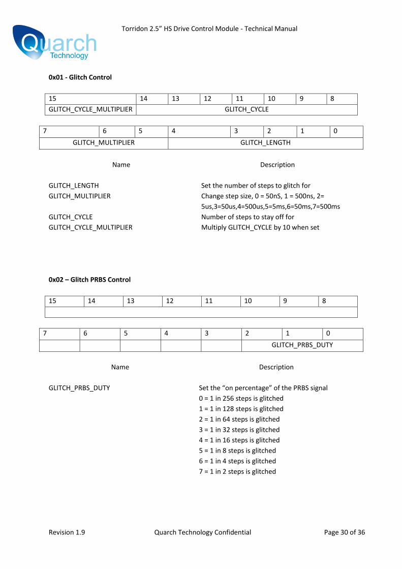
0x01 - Glitch Control
15 14 13 12 11 10 9 8
GLITCH_CYCLE_MULTIPLIER GLITCH_CYCLE
7 6 5 4 3 2 1 0
GLITCH_MULTIPLIER GLITCH_LENGTH
Name Description
GLITCH_LENGTH Set the number of steps to glitch for
GLITCH_MULTIPLIER Change step size, 0 = 50nS, 1 = 500ns, 2=
5us,3=50us,4=500us,5=5ms,6=50ms,7=500ms
GLITCH_CYCLE Number of steps to stay off for
GLITCH_CYCLE_MULTIPLIER Multiply GLITCH_CYCLE by 10 when set
0x02 – Glitch PRBS Control
15 14 13 12 11 10 9 8
7 6 5 4 3 2 1 0
GLITCH_PRBS_DUTY
Name Description
GLITCH_PRBS_DUTY Set the “on percentage” of the PRBS signal
0 = 1 in 256 steps is glitched
1 = 1 in 128 steps is glitched
2 = 1 in 64 steps is glitched
3 = 1 in 32 steps is glitched
4 = 1 in 16 steps is glitched
5 = 1 in 8 steps is glitched
6 = 1 in 4 steps is glitched
7 = 1 in 2 steps is glitched
Torridon 2.5” HS Drive Control Module - Technical Manual
Revision 1.9 Quarch Technology Confidential Page 31 of 36
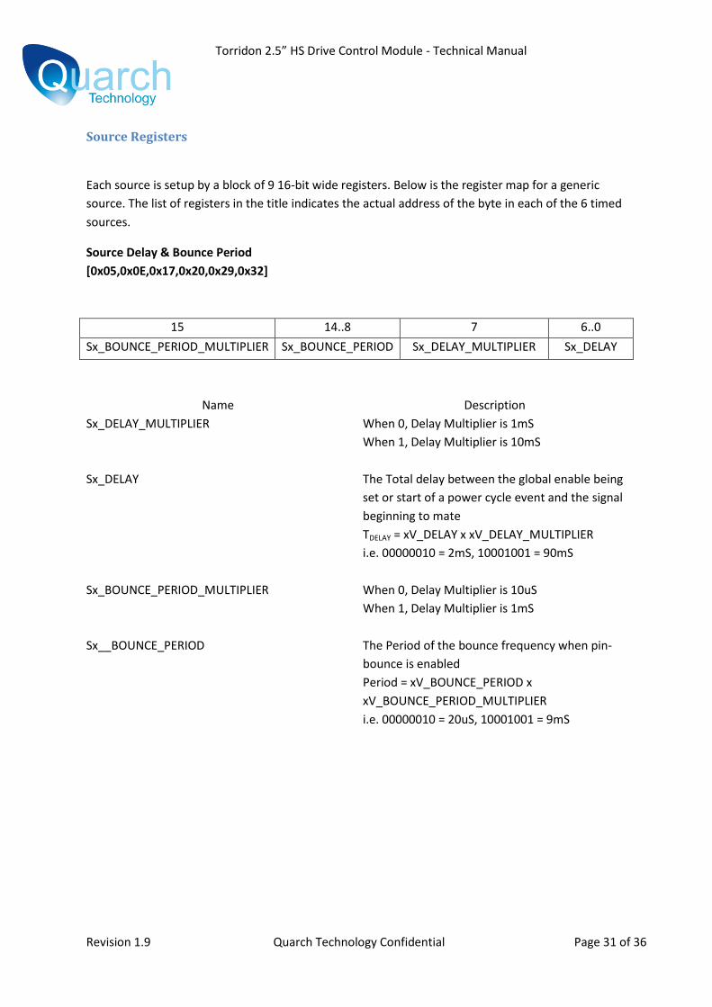
Source Registers
Each source is setup by a block of 9 16-bit wide registers. Below is the register map for a generic
source. The list of registers in the title indicates the actual address of the byte in each of the 6 timed
sources.
Source Delay & Bounce Period
[0x05,0x0E,0x17,0x20,0x29,0x32]
15 14..8 7 6..0
Sx_BOUNCE_PERIOD_MULTIPLIER Sx_BOUNCE_PERIOD Sx_DELAY_MULTIPLIER Sx_DELAY
Name Description
Sx_DELAY_MULTIPLIER When 0, Delay Multiplier is 1mS
When 1, Delay Multiplier is 10mS
Sx_DELAY The Total delay between the global enable being
set or start of a power cycle event and the signal
beginning to mate
TDELAY = xV_DELAY x xV_DELAY_MULTIPLIER
i.e. 00000010 = 2mS, 10001001 = 90mS
Sx_BOUNCE_PERIOD_MULTIPLIER When 0, Delay Multiplier is 10uS
When 1, Delay Multiplier is 1mS
Sx__BOUNCE_PERIOD The Period of the bounce frequency when pin-
bounce is enabled
Period = xV_BOUNCE_PERIOD x
xV_BOUNCE_PERIOD_MULTIPLIER
i.e. 00000010 = 20uS, 10001001 = 9mS
Torridon 2.5” HS Drive Control Module - Technical Manual
Revision 1.9 Quarch Technology Confidential Page 32 of 36
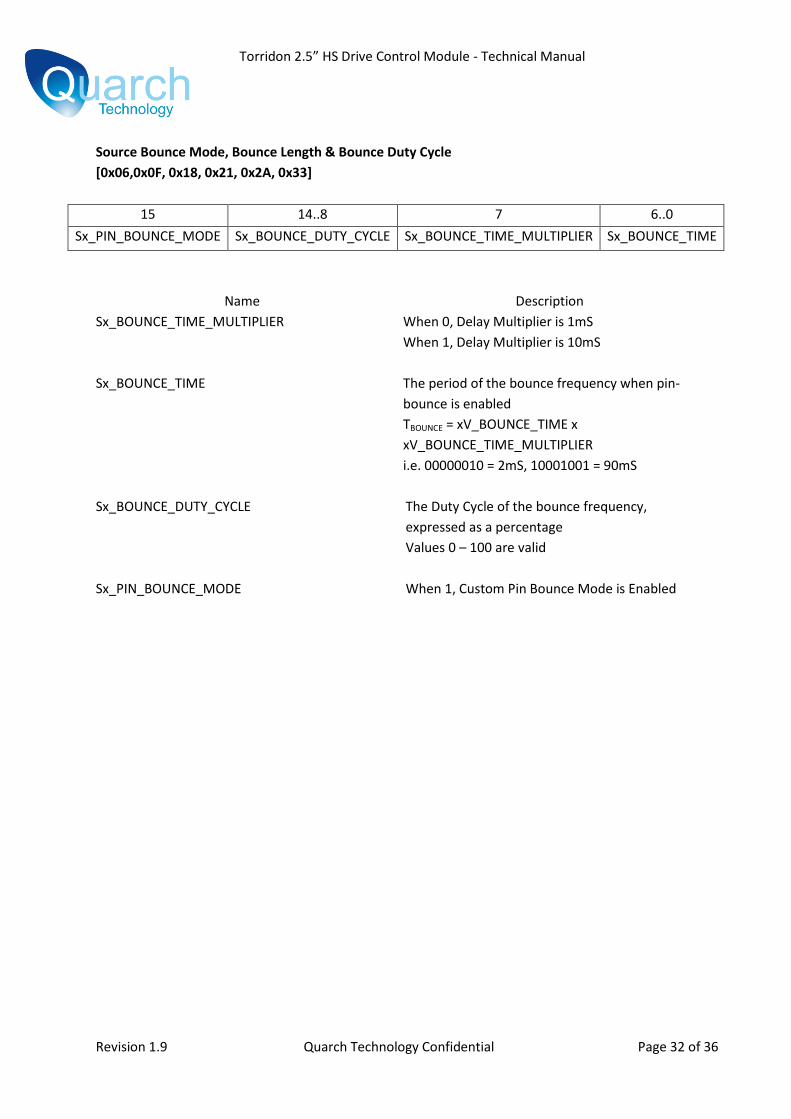
Source Bounce Mode, Bounce Length & Bounce Duty Cycle
[0x06,0x0F, 0x18, 0x21, 0x2A, 0x33]
15 14..8 7 6..0
Sx_PIN_BOUNCE_MODE Sx_BOUNCE_DUTY_CYCLE Sx_BOUNCE_TIME_MULTIPLIER Sx_BOUNCE_TIME
Name Description
Sx_BOUNCE_TIME_MULTIPLIER When 0, Delay Multiplier is 1mS
When 1, Delay Multiplier is 10mS
Sx_BOUNCE_TIME The period of the bounce frequency when pin-
bounce is enabled
TBOUNCE = xV_BOUNCE_TIME x
xV_BOUNCE_TIME_MULTIPLIER
i.e. 00000010 = 2mS, 10001001 = 90mS
Sx_BOUNCE_DUTY_CYCLE The Duty Cycle of the bounce frequency,
expressed as a percentage
Values 0 – 100 are valid
Sx_PIN_BOUNCE_MODE When 1, Custom Pin Bounce Mode is Enabled
Torridon 2.5” HS Drive Control Module - Technical Manual
Revision 1.9 Quarch Technology Confidential Page 33 of 36
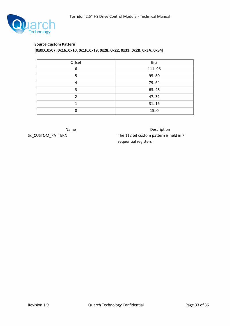
Source Custom Pattern
[0x0D..0x07, 0x16..0x10, 0x1F..0x19, 0x28..0x22, 0x31..0x2B, 0x3A..0x34]
Offset Bits
6 111..96
5 95..80
4 79..64
3 63..48
2 47..32
1 31..16
0 15..0
Name Description
Sx_CUSTOM_PATTERN The 112 bit custom pattern is held in 7
sequential registers
Torridon 2.5” HS Drive Control Module - Technical Manual
Revision 1.9 Quarch Technology Confidential Page 34 of 36
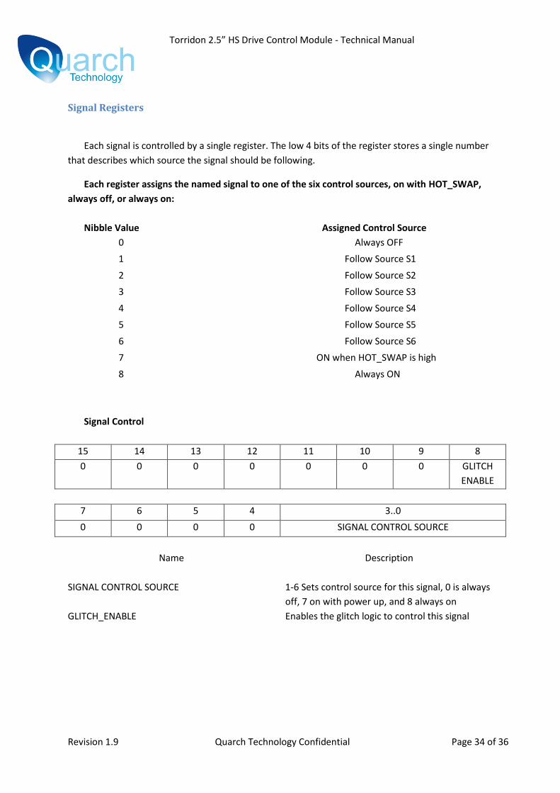
Signal Registers
Each signal is controlled by a single register. The low 4 bits of the register stores a single number
that describes which source the signal should be following.
Each register assigns the named signal to one of the six control sources, on with HOT_SWAP,
always off, or always on:
Nibble Value Assigned Control Source
0 Always OFF
1 Follow Source S1
2 Follow Source S2
3 Follow Source S3
4 Follow Source S4
5 Follow Source S5
6 Follow Source S6
7 ON when HOT_SWAP is high
8 Always ON
Signal Control
15 14 13 12 11 10 9 8
0 0 0 0 0 0 0 GLITCH
ENABLE
7 6 5 4 3..0
0 0 0 0 SIGNAL CONTROL SOURCE
Name Description
SIGNAL CONTROL SOURCE 1-6 Sets control source for this signal, 0 is always
off, 7 on with power up, and 8 always on
GLITCH_ENABLE Enables the glitch logic to control this signal
Torridon 2.5” HS Drive Control Module - Technical Manual
Revision 1.9 Quarch Technology Confidential Page 35 of 36
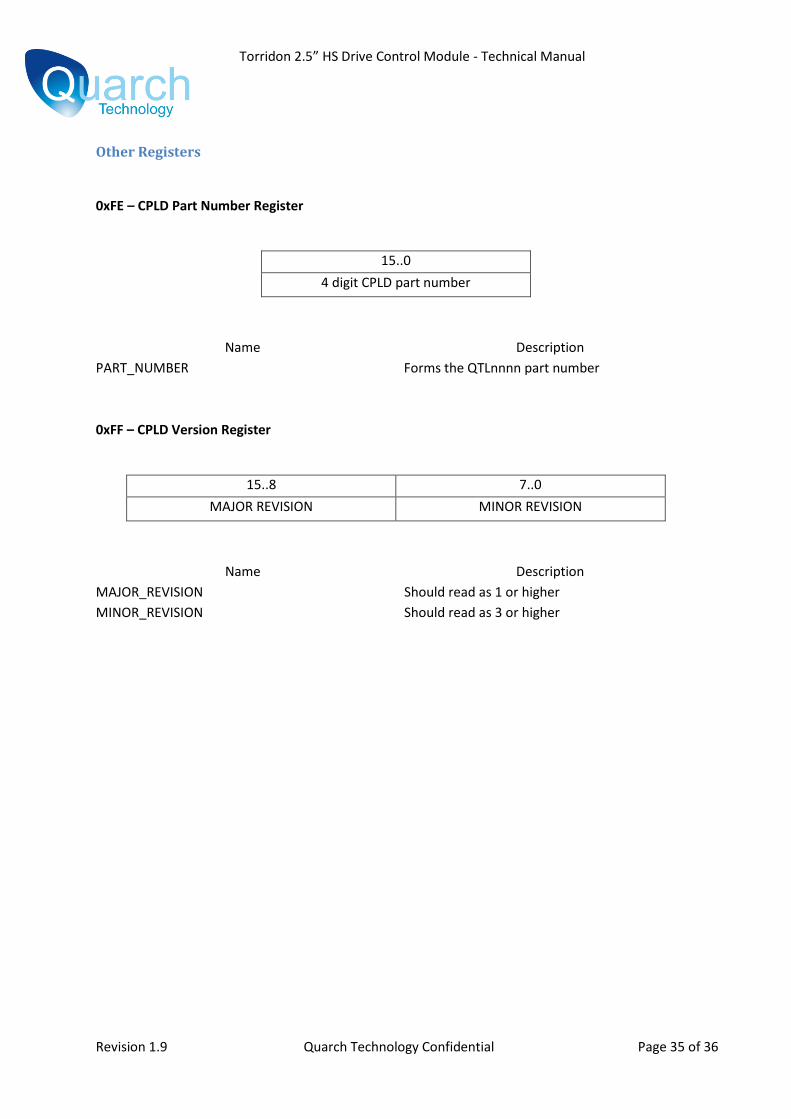
Other Registers
0xFE – CPLD Part Number Register
15..0
4 digit CPLD part number
Name Description
PART_NUMBER Forms the QTLnnnn part number
0xFF – CPLD Version Register
15..8 7..0
MAJOR REVISION MINOR REVISION
Name Description
MAJOR_REVISION Should read as 1 or higher
MINOR_REVISION Should read as 3 or higher

Torridon 2.5” HS Drive Control Module - Technical Manual
Revision 1.9 Quarch Technology Confidential Page 36 of 36
Appendix 1 - Signal Names
The following signal names are used to specify a single signal or a group of signals. These may be
used in commands that take a parameter “SIGNAL_NAME”. Note that some commands, such as
those returning a value, only accept a parameter that resolves to a single signal. In this case you
cannot use the group names
Signals
3V3_POWER
3V3_CHARGE
5V_POWER
5V_CHARGE
12V_POWER
12V_CHARGE
SPECIAL1 (MATED on GND7)
PRI_OUT_PL (Backplane primary out +ve)
PRI_OUT_MN (Backplane primary out -ve)
PRI_IN_PL (Backplane primary in +ve)
PRI_IN_MN (Backplane primary in -ve)
SEC_OUT_PL (Backplane secondary out +ve)
SEC_OUT_MN (Backplane secondary out -ve)
SEC_IN_PL (Backplane secondary in +ve)
SEC_IN_MN (Backplane secondary in -ve)
Signal Groups
ALL (Allows change of all signals at the same time)